

Page 1
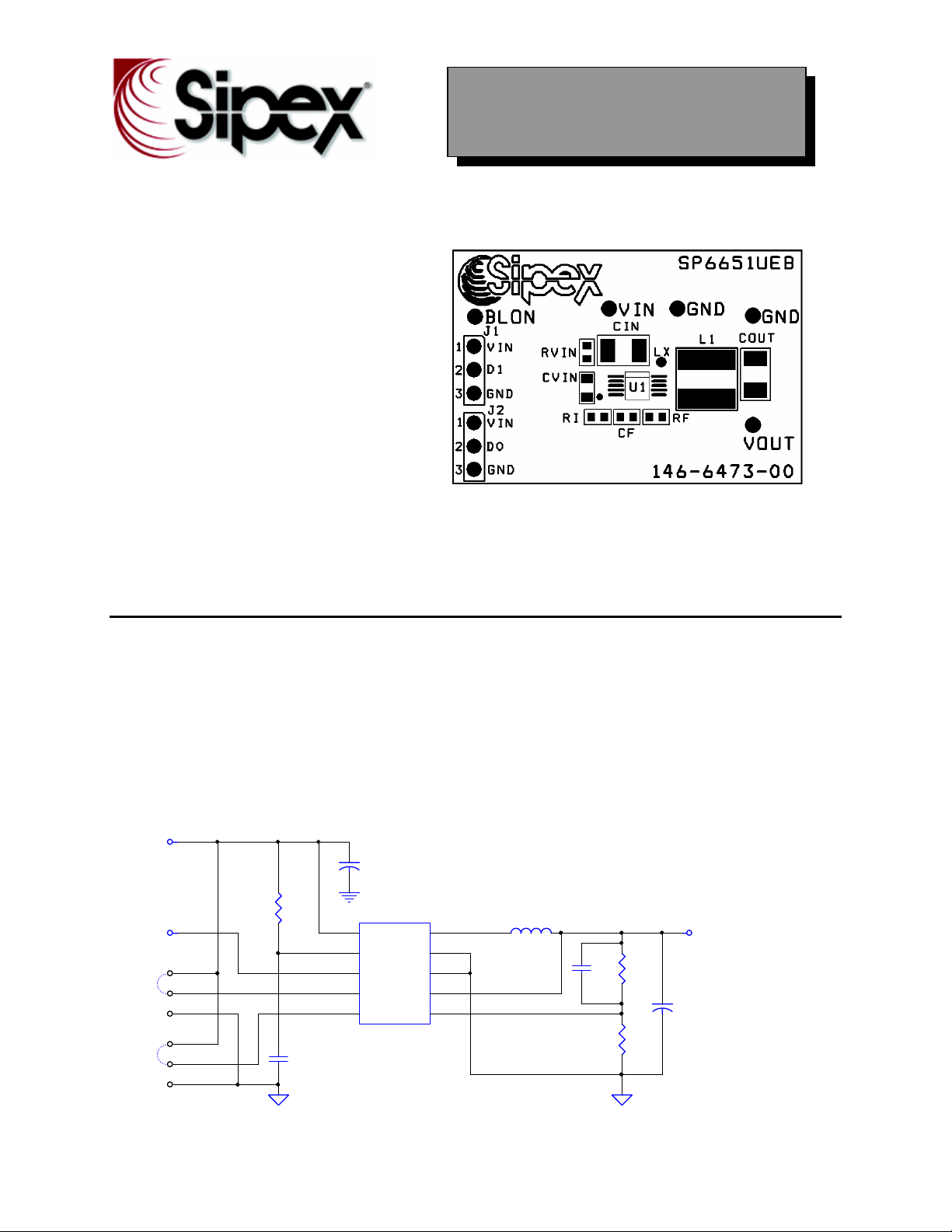
SP6651EB
Evaluation Board Manual
High Efficiency Synchronous
Step-Down Converter with up to
98% efficiency
800mA Output Current, only
20uA Quiescent Current
2.7V-6.5V Input Voltage range,
Output Adjustable down to 0.8V
MSOP Package & Ceramic
Capacitors for small, low profile
Power Supply
Ideal for PDAs, Digital Cameras,
Wireless Modems, Cellular
Telephones
DESCRIPTION
The SP6651A Evaluation Board is designed to help the user evaluate the performance
of the SP6651A for use as a single Li-Ion battery Step-Down DC-DC Converter. The
SP6651A operates from 2.7V to 6.5V input, with the highest efficiency in the range 3.0V
to 4.2V where the Li-Ion battery has the most energy. The SP6651A evaluation board
is a complete power supply circuit to provide ease of evaluation for the DC/DC
Converter performance.
FIGURE 1. SP6651A 3.3V OUTPUT EVALUATION BOARD SCHEMATIC
Vin 2.7 - 6.5VDC
CIN
22uF
RV IN
D1
D0
BLON
J1
J2
10.0
1
2
3
1
2
3
CV IN
1.0uF
U1
1
PV i n
2
Vin
3
BLON
4
D1
5 6
D0 FB
SP6651A
LX
PGN D
GND
Vout
L1
10
9
8
7
10uH
CF
22pF
Vout 3.3V 800mA
RF
825K
COUT
RI
261K
22uF
1
Page 2
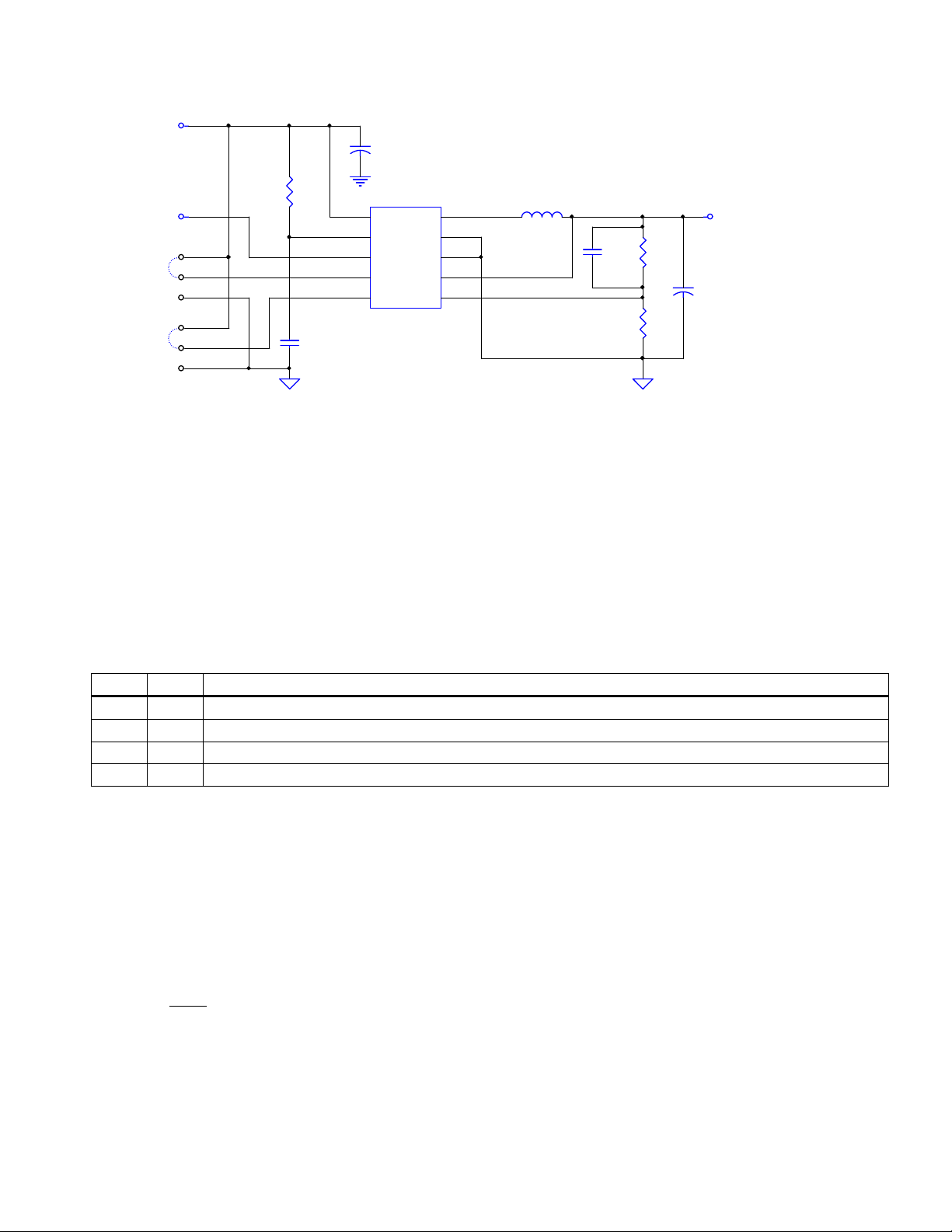
FIGURE 2. SP6651A 1.5V OUTPUT EVALUATION BOARD SCHEMATIC
Vin 2.7 - 6.5VDC
CIN
22uF
RV IN
D1
D0
BLON
J1
J2
10.0
1
2
3
1
2
3
CV IN
1.0uF
U1
1
PV i n
2
Vin
3
BLON
4
D1
5 6
D0 FB
SP6651A
LX
PGN D
GND
Vout
L1
10
9
8
7
10uH
CF
22pF
Vout 1.5V 800mA
RF
226K
COUT
RI
261K
22uF
USING THE EVALUATION BOARD
1) Powering up the SP6651A Circuit & Programming the UVLO threshold
The SP6651A Evaluation Board can be powered from a single Li-Ion battery or a +2.7 to
+6.5V power supply. Connect with short leads directly to the “Vin” and “Gnd” posts.
Note the SP6651A will remain in “shutdown” until D0 or D1 of the Jumpers J1 or J2 are
applied to the Vin or position 1 to 2. See Table 1 for UVLO threshold programming and
D1 and D0 pin definition.
Table 1. Operating Mode Definition
D1 D0 Definition
0 0 Shutdown. All internal circuitry is disabled and the power switches are opened.
0 1 Device enabled, falling UVLO threshold = 2.70V
1 0 Device enabled, falling UVLO threshold = 2.85V
1 1 Device enabled, falling UVLO threshold = 3.00V
2) VOUT PROGRAMMING
The SP6651A requires 2 feedback resistors to control the output voltage. Connect the
appropriate resistors RF and RI (Table 2) from pin 6 SP6651A FB to Vout and to the
GND.
For Vout different from that shown in the Table 2, use equation:
Vout
RF •
RI
−= 1
8.0
2
Page 3
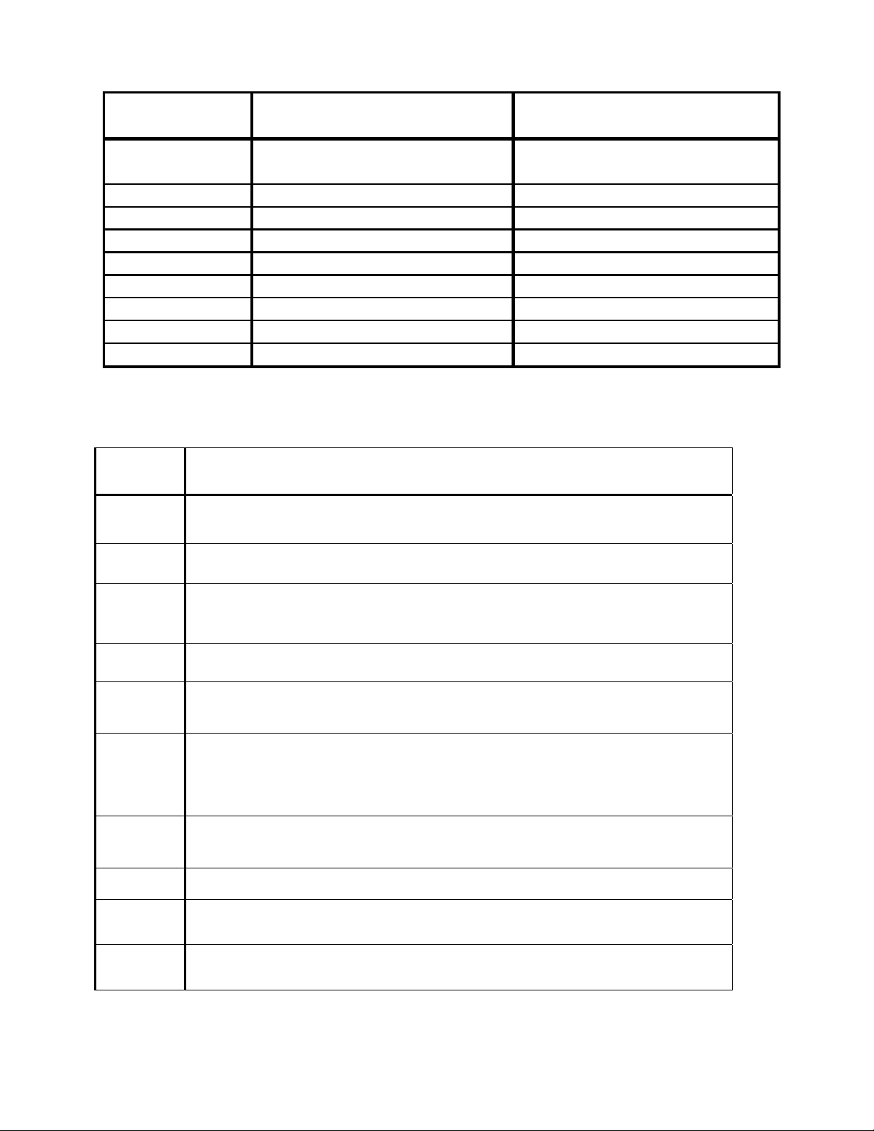
Table 2. SP6651EB BILL OF MATERIALS
Component Vo = 3.3V Vo = 1.5V
L1 10uH, CDRH5D28-100, Sumida 10uH, CDRH5D28-100, Sumida
CIN 22uF, TDK C3225X5R0J226M 22uF, TDK C3225X5R0J226M
COUT 22uF, TDK C3225X5R0J226M 22uF, TDK C3225X5R0J226M
RVIN 10 Ohm 5% 10 Ohm 5%
CVIN 1uF ceramic X7R SM 0805 1uF ceramic X7R SM 0805
RI 261k 1% 261k 1%
RF 825k 1% 226k 1%
CF 22pF ceramic 22pF ceramic
U1 SP6651AEU SP6651AEU
Table 3. SP6651A PIN ASSIGNMENT
Pin
Name
Pin Description
Pin
NO.
PVin
Vin
BLON
D1
D0
FB
Vout
GND
PGND
Input voltage power pin. Inductor charging current passes
through this pin.
Internal supply voltage. Control circuitry powered from this
pin.
Open drain battery low output – need to pullup to supply
externally. Vin - Vout below threshold pulls this node to
ground. Vin - Vout above threshold, this node is open.
Digital mode control input. See Table 1 for definition.
Digital mode control input. See Table 1 for definition.
External feedback network input connection. Connect a
resistor from FB to ground and FB to Vout to control the
output voltage. This pin regulates to the internal reference
voltage of 0.8V.
Output voltage sense pin. Used for internal timing and BLON
circuitry.
Internal ground pin. Control circuitry returns current to this pin.
Power ground pin. Synchronous rectifier current returns
through this pin.
1
2
3
4
5
6
7
8
9
LX
Inductor switching node. Inductor tied between this pin and
the output capacitor to create Vout.
3
10
Page 4
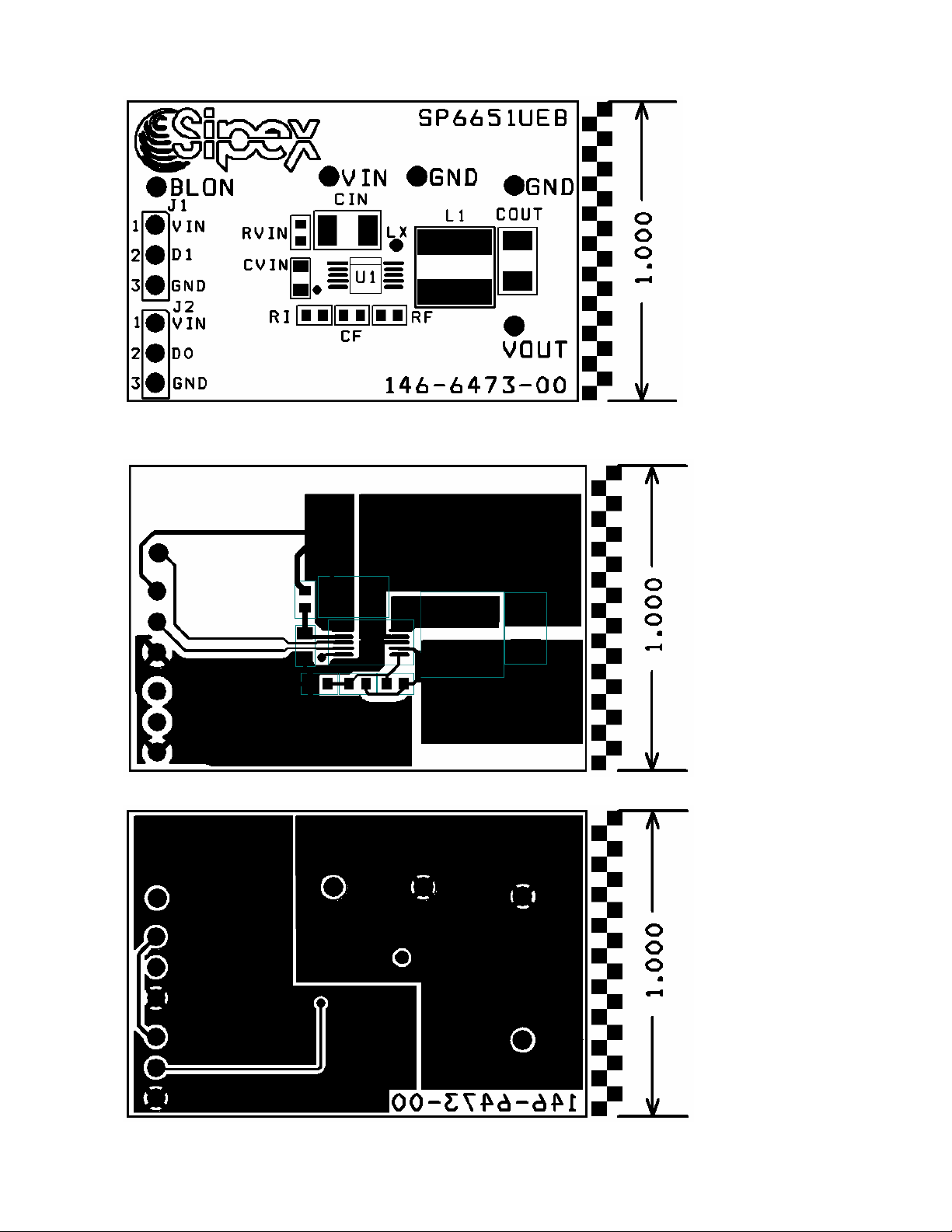
EVALUATION BOARD LAYOUT
FIGURE 3: SP6651AEU COMPONENT PLACEMENT
FIGURE 4: SP6651AEU PC LAYOUT TOP SIDE
FIGURE 5: SP6651AEU PC LAYOUT BOTTOM SIDE
4
Page 5

ORDERING INFORMATION
Model Temperature Range Package Type
SP6651EB ...........................…..-40°C to +85°C....................SP6651 Evaluation Board
5
 Loading...