

Page 1
Reversion
From
To
VBOX-3200
In-Vehicle Computing
User's Manual
Version 1.2
Document Name
Version
Reversion History :
1.0 Jun 08, 2011 Initial document issued Stanley Chou
1.1 Jun 25, 2012 Add CAN Pin assignment Stanley Chou
1.1 1.2 Sept 27, 2012 M12 Connecting to the Network Stanley Chou
VBOX-3200 User Manual
1.2
Date Notes Author(s)
Document No.
Date
UM2011320012
Sept. 27, 2012
Page 2

SINTRONES® Technology Corp.
User Manual
Copyright
©2009 by SINTRONES® Technology Corp. All Rights Reserved.
No part of this publication may be reproduced, transcribed, stored in a retrieval system,
translated into any language, or transmitted in any form or by any means such as
electronic, mechanical, magnetic, optical, chemical, photocopy, manual, or otherwise,
without prior written permission from SINTRONES® Technology Corp.
Other brands and product names used herein are for identification purposes only and
may be trademarks of their respective owners.
Disclaimer
SINTRONES® Technology Corp. shall not be liable for any incidental or consequential
damages resulting from the performance or use of this product.
SINTRONES® Technology Corp. makes no representation or warranty regarding the
content of this manual. Information in this manual had been carefully checked for
accuracy; however, no guarantee is given as to the correctness of the contents. For
continuing product improvement, SINTRONES® Technology Corp. reserves the right to
revise the manual or make changes to the specifications of this product at any time
without notice and obligation to any person or entity regarding such change. The
information contained in this manual is provided for general use by customers.
This device complies to Part 15 of the FCC Rules. Operation is subject to the following
two conditions:
1. This device may not cause harmful interference.
2. This device must withstand any background interference including those that may
cause undesired operation.
User’s Manual Page i
Page 3

Safety Information
Read the following precautions before setting up a SINTRONES Product.
Electrical safety
To prevent electrical shock hazard, disconnect the power cable from the electrical
outlet before relocating the system.
When adding or removing devices to or from the system, ensure that the power
cables for the devices are unplugged before the signal cables are connected. If
possible, disconnect all power cables from the existing system before you add a
device.
Before connecting or removing signal cables from the motherboard, ensure that all
power cables are unplugged.
Seek professional assistance before using an adapter or extension cord. These
devices could interrupt the grounding circuit.
Make sure that your power supply is set to the correct voltage in your area. If you
are not sure about the voltage of the electrical outlet you are using, contact your
local power company.
If the power supply is broken, do not try to fix it by yourself. Contact a qualified
service technician or your retailer.
Operation safety
Before installing the motherboard and adding devices on it, carefully read all the
manuals that came with the package.
Before using the product, make sure all cables are correctly connected and the
power cables are not damaged. If you detect any damage, contact your dealer
immediately.
To avoid short circuits, keep paper clips, screws, and staples away from
connectors, slots, sockets and circuitry.
Avoid dust, humidity, and temperature extremes. Do not place the product in any
area where it may become wet.
Place the product on a stable surface.
If you encounter technical problems with the product, contact a qualified service
technician or your retailer.
User’s Manual Page ii
Page 4

CAUTION
Incorrectly replacing the battery may damage this computer. Replace only with the
same or its equivalent as recommended by SINTRONES® Technology Corp. Dispose used
battery according to the manufacturer's instructions.
Technical Support
Please do not hesitate to call or e-mail our customer service when you still cannot fix
the problems.
Tel : +886-2-82280101
Fax : +886-2-82280100
E-mail : [email protected]
Website : www.sintrones.com
User’s Manual Page iii
Page 5

TABLE OF CONTENTS
1.0
Introduction ............................................................................................................................... 1-1
1.1 Model Specification .............................................................................................................. 1-1
1.2 VBOX-3200 Illustration (MB, System) .............................................................................. 1-3
2.0 Internal Connector Specification ............................................................................................ 2-1
2.1 SATA Power Wafer Connector ........................................................................................... 2-1
2.2 Reserved JST Connector ...................................................................................................... 2-1
2.3 COM Port JST Connector (COM2) ....................................................................................... 2-2
2.4 COM Port JST Connector (COM3) ....................................................................................... 2-2
2.5 COM Port JST Connector (COM4) ....................................................................................... 2-3
2.6 DVI-D /LVDS connector: (DP0) .......................................................................................... 2-4
Page #
2.7 VGA JST Connector ............................................................................................................... 2-5
2.8 SATA Connector (SATA1) .................................................................................................... 2-5
2.9 SATA Connector (SATA0) .................................................................................................... 2-6
2.10 USB JST Connector (USB4/5) ............................................................................................. 2-6
2.11 USB JST Connector (USB 6/7)............................................................................................. 2-7
2.12 UPS JST Connector ................................................................................................................ 2-7
2.13 Download Port JST Connector ........................................................................................... 2-8
2.14 BATTERY Connector (Recommend to use CR2032 Battery) ....................................... 2-8
2.15 RTC RESET Connector .......................................................................................................... 2-9
2.16 RS232 RI# Pin Power Select Connector (COM2) ............................................................ 2-9
2.17 RS232 RI# Pin Power Select Connector (COM1) .......................................................... 2-10
2.18 MINI CARD Connector (Mini Card0) ............................................................................... 2-10
2.19 Mini CARD Connector (Mini Card1) ................................................................................ 2-12
2.20 MINI CARD Connector (Mini Card2) ............................................................................... 2-13
3.0 External Connector Specification ............................................................................................ 3-1
3.1 Power Input Connector ....................................................................................................... 3-1
3.2 Power Button Connector .................................................................................................... 3-2
3.3 DIO Connector ....................................................................................................................... 3-2
3.4 RJ45 Connector (LAN0) ....................................................................................................... 3-3
3.5 RJ45 Connector (LAN1) ....................................................................................................... 3-4
User’s Manual Page iv
Page 6

3.6 M12 Connecting to the Network ........................................................................................ 3-4
3.7 COM Port Connector (COM1).............................................................................................. 3-5
3.8 DVI-I Connector (DP1+VGA)............................................................................................... 3-6
3.9 USB Connector (USB 0/1) ................................................................................................... 3-7
3.10 USB Connector (USB2/3) .................................................................................................... 3-8
3.11 Audio Connector ................................................................................................................... 3-8
3.12 CAN Pin Assignment ............................................................................................................. 3-9
3.13 UPS/3.5G LED ........................................................................................................................ 3-9
3.14 HDD/ACC LED ...................................................................................................................... 3-10
3.15 CAN BUS Pin Assignment .................................................................................................. 3-10
4.0 System Installation ................................................................................................................... 4-1
4.1 System Introduction ............................................................................................................ 4-1
4.2 Opening Chassis .................................................................................................................... 4-2
4.3 Installing Memory ................................................................................................................ 4-6
4.4 Installing MINI PCIe Expansion Card (PCIe 1) ................................................................ 4-9
4.5 Installing MINI PCIe Expansion Card (PCIe 2, Wifi Module) ...................................... 4-11
4.6 Installing MINI PCIe Expansion Card (PCIe 3, 3G Module only) ................................ 4-13
4.7 Installing Internal Antenna Cable ................................................................................... 4-15
4.8 Installing SIM Card ............................................................................................................. 4-19
4.9 Installing HDD ..................................................................................................................... 4-21
5.0 System Resource ........................................................................................................................ 5-1
5.1 Ignition Power Management Quick Guide ....................................................................... 5-1
5.2 GPIO & Delay Time Setting ................................................................................................. 5-3
5.2.1 GPIO, Delay Time and Ignition Control Register ............................................................................ 5-3
5.2.2 GPIO Programming Procedure ........................................................................................................ 5-4
5.2.3 WDT Setting ...................................................................................................................................... 5-5
5.3 Gobi2000 WWAN Module Application Note .................................................................... 5-8
5.4 Gobi2000 GPS Module Application Note ........................................................................ 5-12
6.0 BIOS ............................................................................................................................................. 6-1
6.1 Super IO Configuration ........................................................................................................ 6-1
7.0 Packing List ................................................................................................................................ 7-1
7.1 Packing List ........................................................................................................................... 7-1
User’s Manual Page v
Page 7

1.0 Introduction
1.0
INTRODUCTION
User’s Manual
Page 8
AMD G-T56N Dual Core 1.6GHz
AMD G-T44R Single Core 1.2GHz (Optional)
2 x Realtek RTL8111E Gb/s Ethernet onboard
Support PXE
1.0 INTRODUCTION
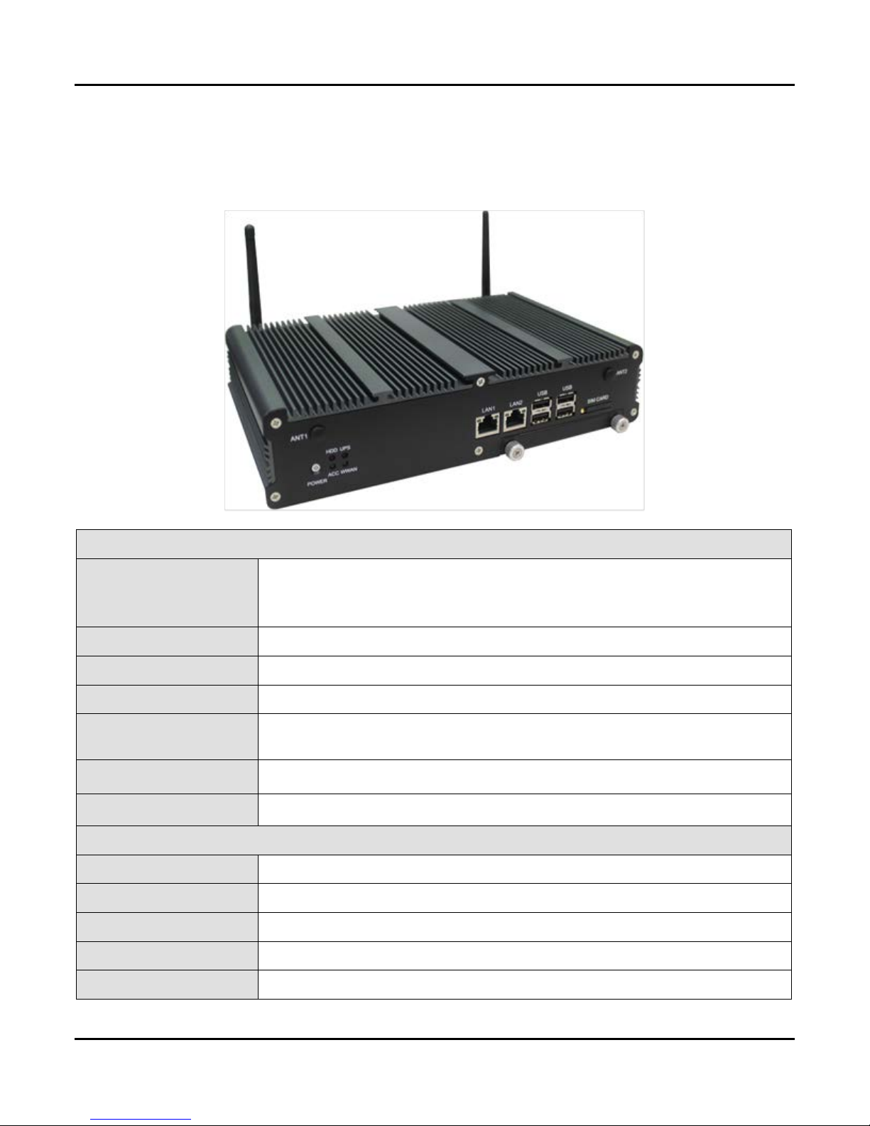
1.1 Model Specification
1.0 Introduction
System
CPU
AMD G-T40N Dual Core 1.0GHz
Memory 2 x DDR3 1333MHz SO-DIMM up to 8GB
Chipset AMD A55E Controller Hub
Graphics AMD G-T56N Radeon HD 6310 / G-T44R Radeon HD 6250
LAN Chipset
Audio Realtek ALC662 HD Codec onboard
Watchdog 1 ~ 255 Level Reset
Power Requirement
Power Input 9V-32V DC Power input
Power Protection Automatics Recovery Short Circuit Protection
Power Management Vehicle Power Ignition for Variety Vehicle
Power Off Control Power off Delay Time Setting by Software
Battery Internal Battery Kit for 10 Mins Operating (Optional)
User’s Manual Page 1-1
Page 9
AMD G-T56N Radeon HD 6310 / G-T44R Radeon HD 6250
1 X DVI-I connector and VGA on rear I/O
3 x RS-232 (COM1,2 with RS-422/485, RS-485 Support Auto Direction
Control)
Operating: MIL-STD-810F, Method 516.5, Procedure I, Trucks and
semi-trailers=40G(11ms), Non-Operating 80G with SSD
Storage
Type 2 x 2.5” drive bay for SATA Type Hard Disk Drive / SSD
Graphics
Graphics
Resolution Up to 2045 x 1560 @85H
Qualification
Certifications CE, FCC, Class A
I/O
Serial Port
USB Port 4 x USB 2.0 Ports on Front I/O
LAN 2 x RJ45 Ports for GbE
1.0 Introduction
Video Port 1 x DVI-I and 1 x VGA Output
DIO Port 4 in and 2 out with Relay 12V / 80mA
Audio 1 x Line-out (Default is 1 on Rear I/O)
SIM Card Socket 1 x SIM Card socket supported onboard with eject
Environment
Operating Temp. -40 ~ 70ºC (SSD), ambient w/ air
Storage Temp. -40 ~ 80ºC
Relative Humidity 10 ~ 95% (non-condensing)
Vibration (random) 2.5g@5~500 Hz with SSD
Vibration Operating MIL-STD-810F, Method 514.5, Category 20, Ground Vehicle-Highway
Truck Storage MIL-STD-810F, Method 514.5, Category 24, Integrity Test
Shock
Crash Hazard MIL-STD-810F, Method 516.5, Procedure V, Ground equipment=100
Mechanical
Construction Aluminum alloy
Mounting Supports both of wall-mount/VESA-mount
Weight 1.5 kg (bard-bone)
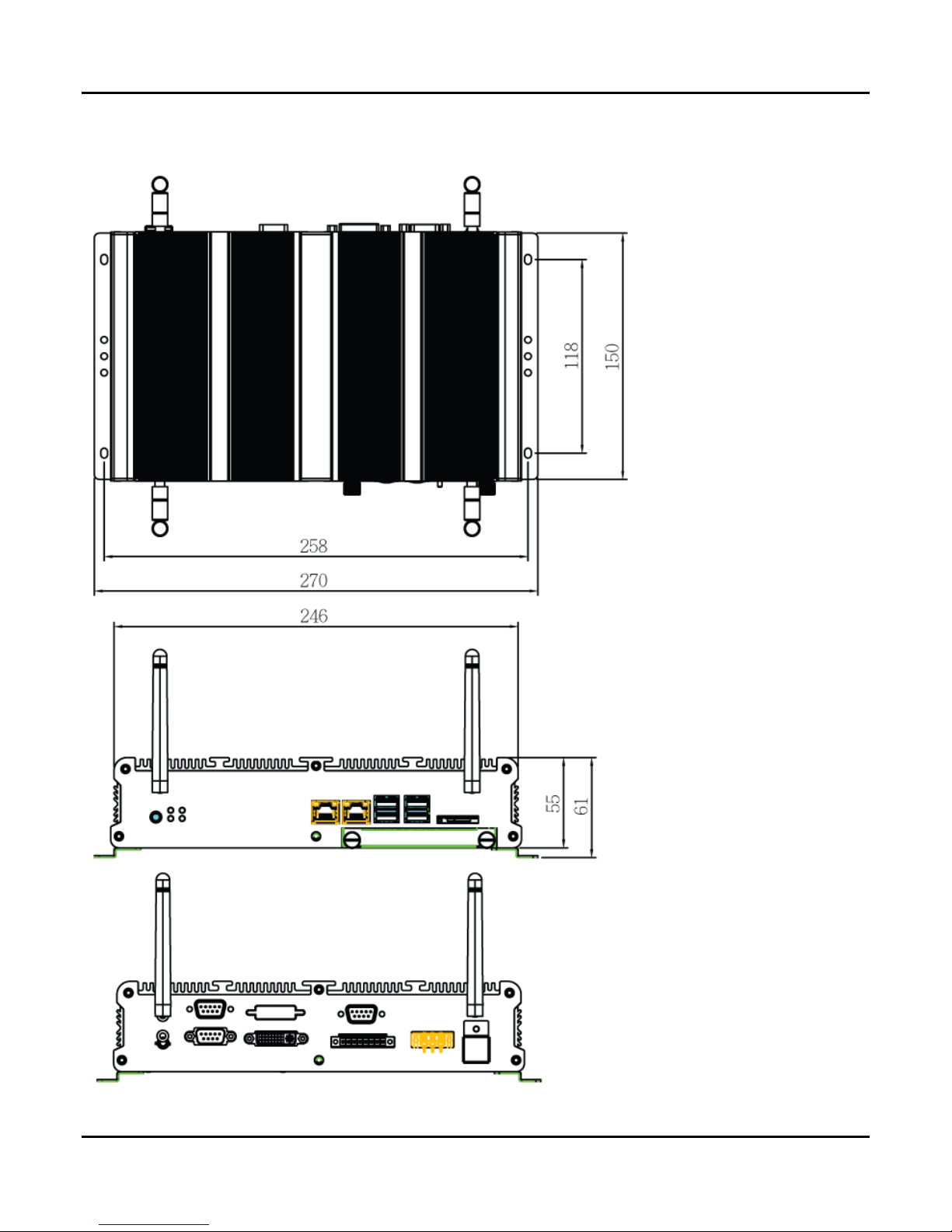
Dimensions 250 x 150 x 55 mm
User’s Manual Page 1-2
Page 10
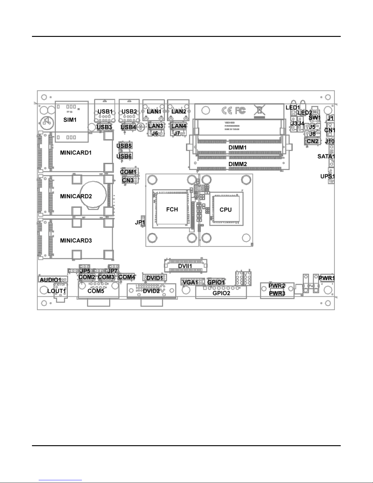
1.2 VBOX-3200 Illustration (MB, System)
Main Board
1.0 Introduction
User’s Manual Page 1-3
Page 11
System
1.0 Introduction
User’s Manual Page 1-4
Page 12

2.0 Internal Connector Specification
2.0
INTERNAL CONNECTOR
SPECIFICATION
User’s Manual
Page 13
Pin
Signal
1
+5V
2
GND
3
GND
4
+12V
Pin
Signal
Pin
Signal
1
SPI_CLK_GPIO0
2
COM6_TX_GPIO5
3
SPI_CS0_GPIO1
4
COM6_RX_GPIO6
5
SPI_MISO_GPIO2
6
GND
7
SPI_MOSI_GPIO3
8
SCLK0
9
SPI_CSI_GPIO4
10
SDATA0
CN1
POWER-2.54mm-M-180
1
2
3
4
CN2
JST-2.0mm-M-180
1
3 4
2
5
6
7 8
9 10
2.0 INTERNAL CONNECTOR SPECIFICATION
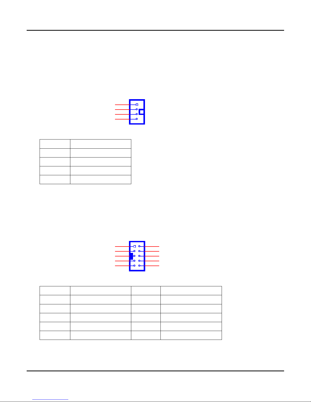
2.1 SATA Power Wafer Connector
A. Connector size: 1 X 4 = 4 Pin
B. Connector location: CN1
C. Connector pin definition
2.0 Internal Connector Specification
2.2 Reserved JST Connector
A. Connector size: 2 X 5 = 10 Pin
B. Connector location: CN2
C. Connector pin definition
User’s Manual Page 2-1
Page 14
Pin
Signal
Pin
Signal
1
COM4_DCD#
2
COM4_RXD
3
COM4_TXD
4
COM4_DTR#
5
GND
6
COM4_DSR#
7
COM4_RTS#
8
COM4_CTS#
9
COM4_RI#
10
GND
Pin
Signal
Pin
Signal
1
COM2_DCD
2
COM2_RXD
3
COM2_TXD
4
COM2_DTR
5
GND
6
COM2_DSR
7
COM2_RTS
8
COM2_CTS
9
COM2_RI/+5V/+12V
10
GND
COM1
JST-2.0mm-M-180
1
3
4
2
5
6
7
8
9
10
COM3
JST-2.0mm-M-180
1
3 4
2
5 6
7
8
9
10
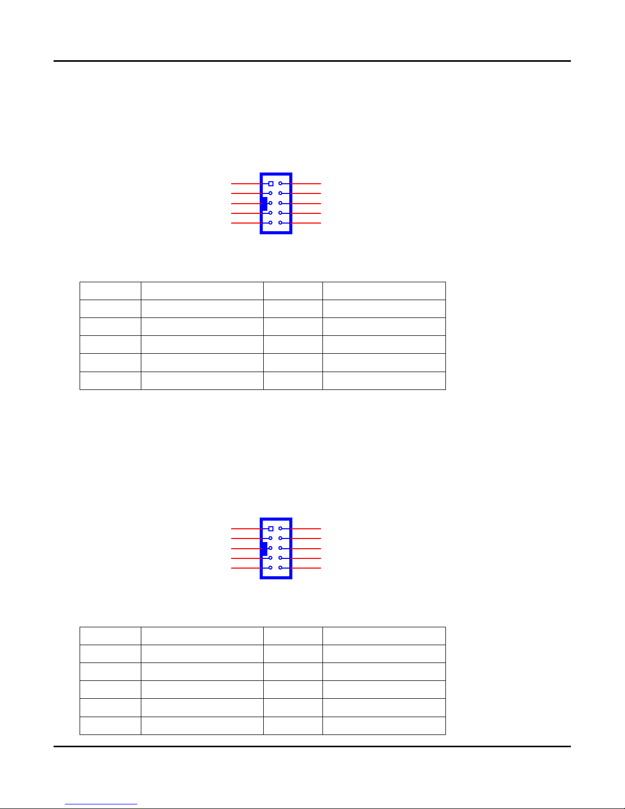
2.3 COM Port JST Connector (COM2)
A. Connector size: 2 X 5 = 10 Pin
B. Connector location: COM2
C. Connector pin definition
2.0 Internal Connector Specification
2.4 COM Port JST Connector (COM3)
A. Connector size: 2 X 5 = 10 Pin
B. Connector location: COM3
C. Connector pin definition (RS-232)
User’s Manual Page 2-2
Page 15

Pin
Signal
Pin
Signal
1
COM2_TXD-
2
COM2_TXD+
3
COM2_RXD+
4
COM2_RXD-
5
NC 6 NC
7
NC 8 NC
9
NC
10
NC
Pin
Signal
Pin
Signal
1
COM2_TXD-/RXD-
2
COM2_TXD+/RXD+
3
NC 4 NC
5
NC 6 NC
7
NC 8 NC
9
NC
10
NC
Pin
Signal
Pin
Signal
1
COM3_DCD
2
COM3_RXD
3
COM3_TXD
4
COM3_DTR
5
GND
6
COM3_DSR
7
COM3_RTS
8
COM3_CTS
9
COM3_RI
10
GND
COM4
JST-2.0mm-M-180
1
3 4
2
5 6
7
8
9 10
D. Connector pin definition (RS-422)
E. Connector pin definition (RS-485)
2.0 Internal Connector Specification
2.5 COM Port JST Connector (COM4)
A. Connector size: 2 X 5 = 10 Pin
B. Connector location: COM4
C. Connector pin definition
User’s Manual Page 2-3
Page 16
Pin
Signal
Pin
Signal
1
DVI_TX0_N /LVDS_TX0_N
2
DVI_TX0_P /LVDS_TX0_P
3
DVI_TX1_N /LVDS_TX1_N
4
DVI_TX1_P /LVDS_TX1_P
5
DVI_TX2_N /LVDS_TX2_N
6
DVI_TX2_P /LVDS_TX2_P
7
GND
8
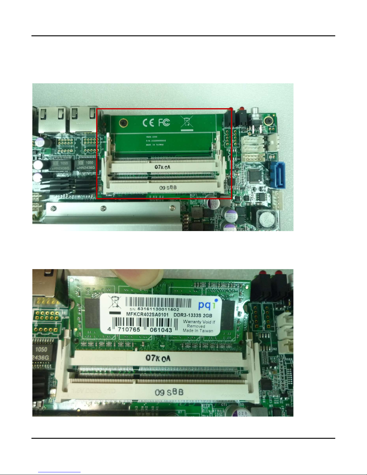
DVI_CLK_N /LVDS_CLK_N
9
DVI_CLK_P /LVDS_CLK_P
10
NC
11
NC
12
NC
13
+5V_DVI_PWR
14
GND
15
+5V_DVI_PWR
16
NC
17
GND
18
NC
19
NC
20
NC
21
+12V_PWR
22
NC
23
+12V_PWR
24
GND
25
GND
26
LVDS_ VDD3
27
DVI_DDC_CLK
28
LVDS_ VDD5
29
DVI_DDC_DATA
30
LVDS_ VDD5
31
DVI_HPD
32
LVDS_ VDD12
33
PWRBT#
34
LVDS_PWM
35
LVDS_BLON
36
GND
37
5VSB_USB
38
USB11_P
39
USB11_N
40
GND_USB
DVII1
DF-1.25mm-M-180
1
1
3
3
5
5
7
7
9
9
11
11
13
13
15
15
17
17
19
19
21
21
23
23
25
25
27
27
29
29
2
2
4
4
6
6
8
8
10
10
12
12
14
14
16
16
18
18
20
20
22
22
24
24
26
26
28
28
30
30
31
31
32
32
33
33
34
34
35
35
36
36
37
37
38
38
39
39
40
40
MGND
H1
MGND
H2
NC
H3
NC
H4
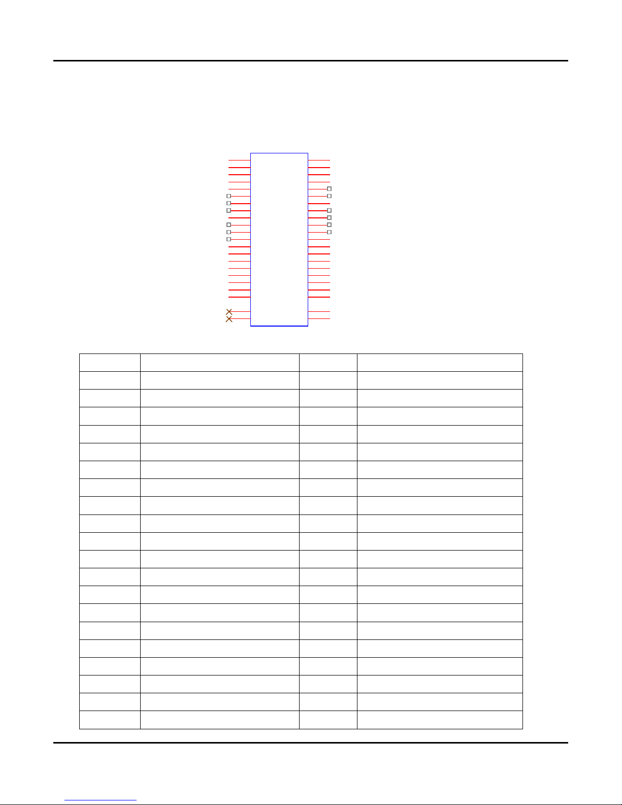
2.6 DVI-D /LVDS connector: (DP0)
A. Connector size: 2 X 20 = 40 Pin
B. Connector location: DVII1
C. Connector pin definition
2.0 Internal Connector Specification
User’s Manual Page 2-4
Page 17

Pin
Signal
Pin
Signal
1
RED
2
GREEN
3
BLUE
4
NC
5
DET
6
GND
7
GND
8
GND
9
+5V
10
GND
11
NC
12
DAC_SDA
13
HSYNC
14
VSYNC
15
DAC_SCL
16
NC
Pin
Signal
2
SATA_TXP1
1
GND
3
SATA_TXN1
4
GND
5
SATA_RXN1
7
GND
6
SATA_RXP1
VGA1
JST-2.0mm-M-180
1
3 4
2
5
6
7 8
9
10
11
13
15
12
14
16
SATA1
SATA-M-180
TXP
2
TXN
3
RXN
5
RXP
6
GND
1
GND
4
GND
7
2.7 VGA JST Connector
A. Connector size: 2 X 8 = 16 Pin
B. Connector location: VGA1
C. Connector pin definition
2.0 Internal Connector Specification
2.8 SATA Connector (SATA1)
A. onnector size: 1 X 7 = 7 Pin (SATA-M-180)
B. Connector location: SATA1
C. Connector pin definition
User’s Manual Page 2-5
Page 18
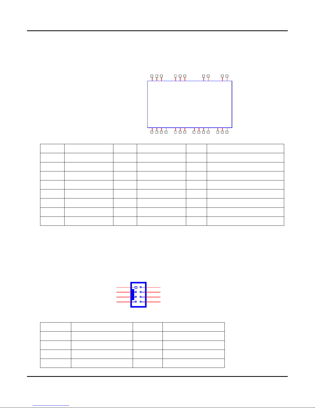
Pin
Signal
Pin
Signal
Pin
Signal
S1
GND
P1
NC
P9
+5V
S2
SATA_TXP0
P2
NC
P10
NC
S3
SATA_TXN0
P3
NC
P11
GND
S4
GND
P4
GND
P12
GND
S5
SATA_RXN0
P5
GND
P13
NC
S6
SATA_RXP0
P6
GND
P14
NC
S7
GND
P7
+5V
P15
P8
+5V
Pin
Signal
Pin
Signal
1
5VSB_USB
2
5VSB_USB
3
USB4_N
4
USB5_N
5
USB4_P
6
USB5_P
7
GND
8
GND
SATA2
SATA-F-22P-90
TX
TX#
RX#
RX
V3.3_1
V3.3_2
V3.3_3
V5_1
V5_2
V5_3
P_Reserve
V12_1
V12_2
V12_3
GND_1S1GND_2
S4
GND_3
S7
GND_4P4GND_5
P5
GND_6
P6
GND_7
P1
GND_8
P1
M1
23
M2
24
USB5
JST-2.0mm-M-180
1
3 4
2
5 6
7 8
2.9 SATA Connector (SATA0)
A. Connector size: SATA-F-22P-90
B. Connector location: SATA2
C. Connector pin definition
2.0 Internal Connector Specification
2.10 USB JST Connector (USB4/5)
A. Connector size: 2 X 5 = 10 Pin
B. Connector location: USB5
C. Connector pin definition
User’s Manual Page 2-6
Page 19
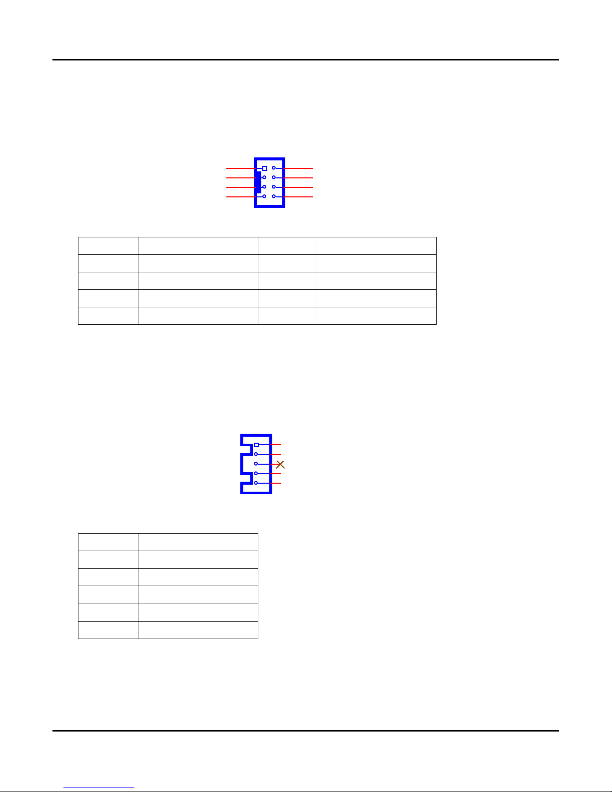
Pin
Signal
Pin
Signal
1
5VSB_USB
2
5VSB_USB
3
USB6_N
4
USB7_N
5
USB6_P
6
USB7_P
7
GND
8
GND
Pin
Signal
1
+12VSB_UPS
2
+12VSB_UPS
3
NC
4
GND
5
GND
USB6
JST-2.0mm-M-180
1
3 4
2
5 6
7
8
UPS1
JST-2.0mm-M-180
1
2
3
4
5
2.11 USB JST Connector (USB 6/7)
A. Connector size: 2 X 5 = 10 Pin
B. Connector location: USB6
C. Connector pin definition
2.0 Internal Connector Specification
2.12 UPS JST Connector
A. Connector size: 1 X 5 = 5 Pin
B. Connector location: UPS1
C. Connector pin definition
User’s Manual Page 2-7
Page 20
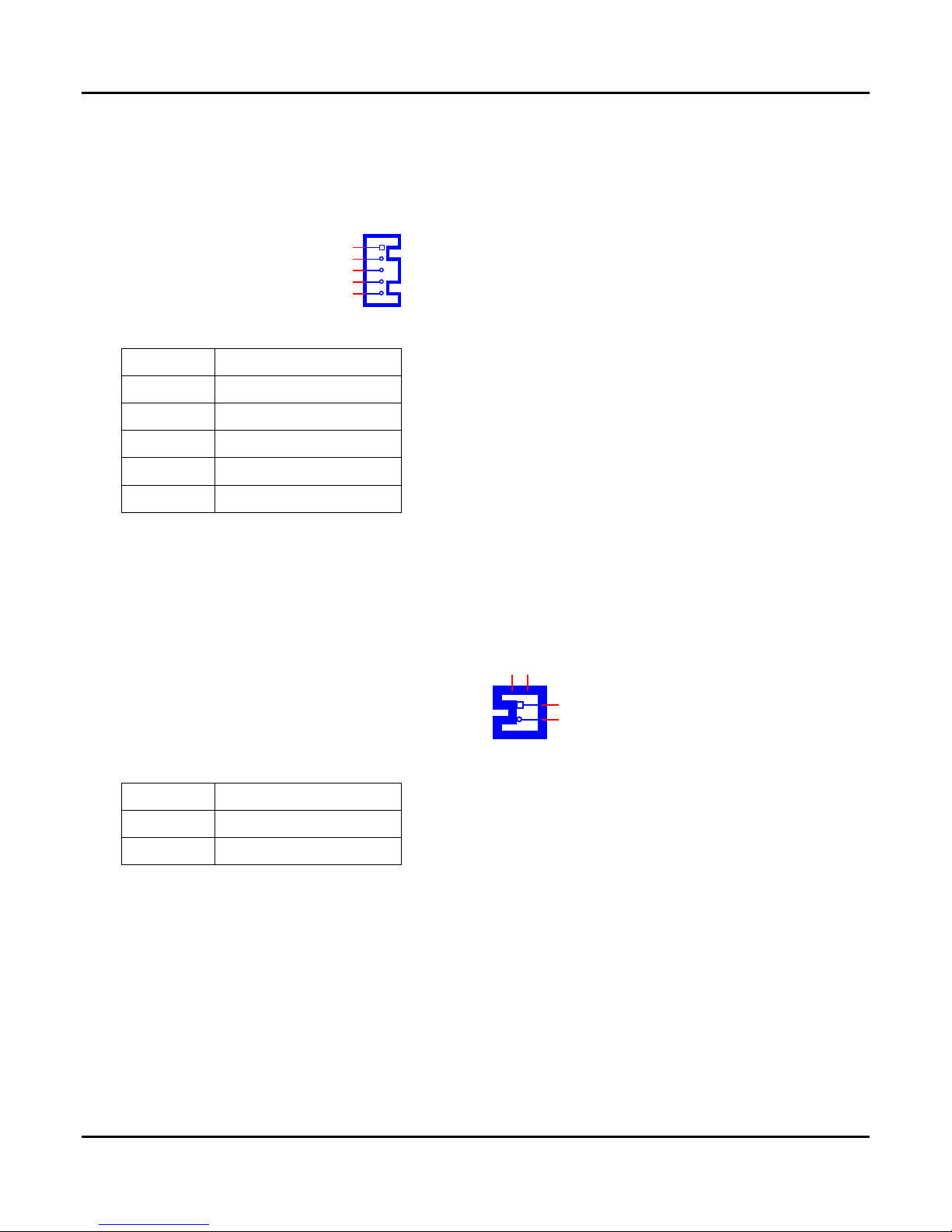
Pin
Signal
1
+3.3V_MCU
2
C2D
3
MRST
4
C2CK
5
GND
Pin
Signal
1
VBAT
2
GND
J5
JST-2.0mm-M-180
1
2
3
4
5
J9
JST-1.25mm-M-180
1
2
3
4
2.13 Download Port JST Connector
A. Connector size: 1 X 5 = 5 Pin
B. Connector location: J5
C. Connector pin definition
2.0 Internal Connector Specification
2.14 BATTERY Connector (Recommend to use CR2032 Battery)
A. Connector size: 1 X 2 = 2 Pin
B. Connector location: J9
C. Connector pin definition
User’s Manual Page 2-8
Page 21
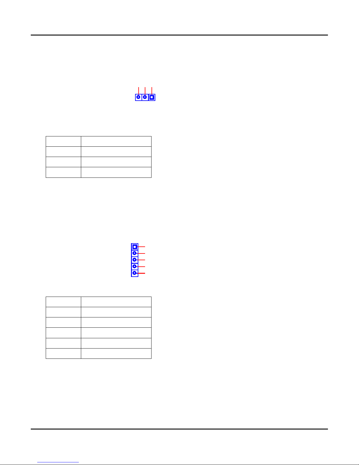
Pin
Signal
1
RTC_BAT
2
RTCRST#
3
GND
Pin
Signal
1
+5V
2
POWER
3
+12V
4
POWER
5
COM2_RI
JP1
PIN-2.54mm-M-180
1
2
3
JP5
PIN-2.0mm-M-180
1
2
3
4
5
2.15 RTC RESET Connector
A. Connector size: 1 X 3 = 3 Pin
B. Connector location: JP1
C. Connector pin definition
2.0 Internal Connector Specification
2.16 RS232 RI# Pin Power Select Connector (COM2)
A. Connector size: 1 X 5 = 5 Pin
B. Connector location: JP5
C. Connector pin definition
User’s Manual Page 2-9
Page 22

Pin
Signal
1
+5V
2
POWER
3
+12V
4
POWER
5
COM1_RI
JP7
PIN-2.0mm-M-180
1
2
3
4
5
MINI PCIE CON
Ver:1.2
MINICARD3
MINICARD
REV1
51
REV2
49
REV3
47
REV4
45
GND14
43
3.3VSB_5
41
3.3VSB_4
39
GND13
37
GND0
35
PETp0
33
PETn0
31
GND2
29
GND3
27
PERp0
25
PERn0
23
GND4
21
REV9/UIM_C4
19
REV10/UIM_C8
17
GND5
15
REFCLK+
13
REFCLK-
11
GND6
9
CLKREQ#
7
COEX2
5
COEX1
3
WAKE#
1
3.3VSB_2
52
GND7
50
1.5V_1
48
LED_WPAN#
46
LED_WLAN#
44
LED_WWAN#
42
GND8
40
USB_D+
38
USB_D-
36
GND9
34
SMBDAT
32
SMBCLK
30
1.5V_2
28
GND10
26
3.3VSB_1
24
PERST#
22
W_DISABLE#
20
GND11
18
UIM_VPP
16
UIM_RESET
14
UIM_CLK
12
UIM_DATA
10
UIM_PWR
8
1.5V_3
6
GND12
4
3.3VSB_3
2
MH1
MH1
MH2
MH2
MH3
MH3
MH4
MH4
MH5
MH5
MH6
MH6
2.17 RS232 RI# Pin Power Select Connector (COM1)
A. Connector size: 1 X 5 = 5 Pin
B. Connector location: JP7
C. Connector pin definition
2.0 Internal Connector Specification
2.18 MINI CARD Connector (Mini Card0)
A. Connector size: 2 X 26 = 52 Pin
B. Connector location: MINICARD3
User’s Manual Page 2-10
Page 23
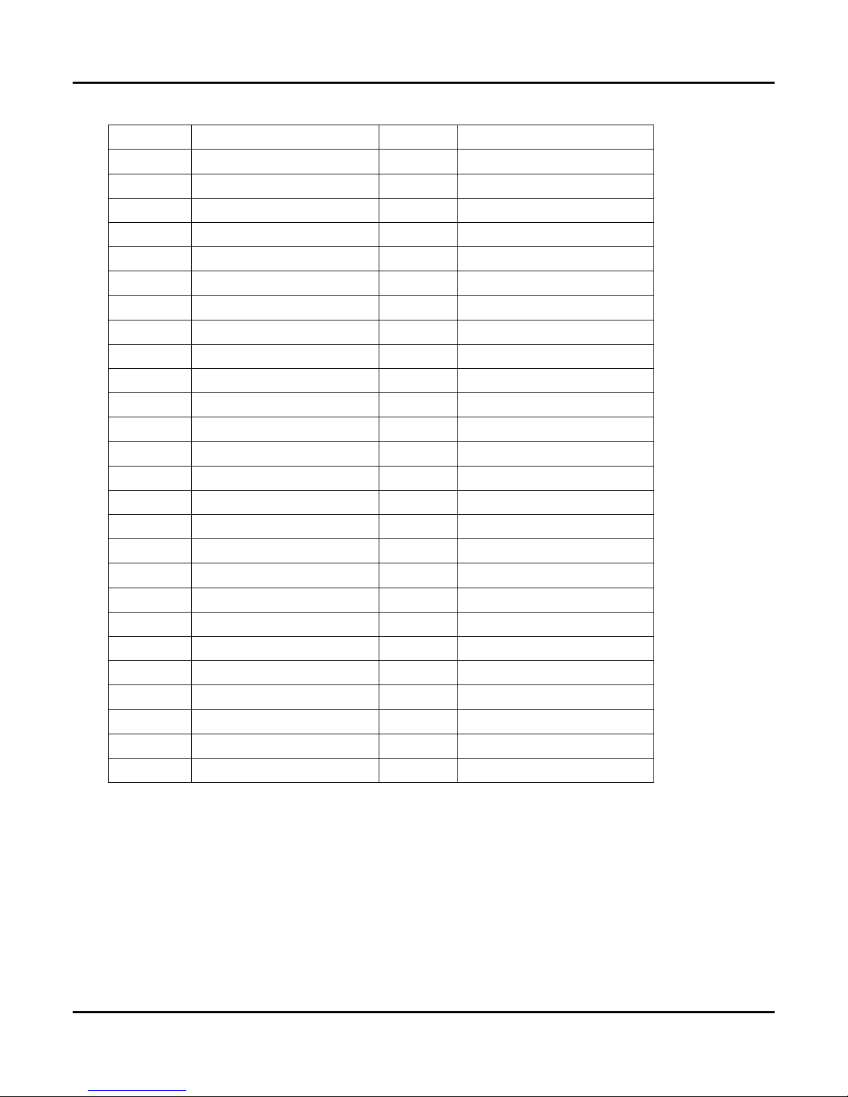
Pin
Signal
Pin
Signal
1
PCIE_WAKE#
2
3VSB
3
NC 4 GND
5
NC 6 +1.5V
7
MINICARD0_CLKREQ#
8
NC
9
GND
10
NC
11
PCIE_MCARD0_CLK_N
12
NC
13
PCIE_MCARD0_CLK_P
14
NC
15
GND
16
NC
17
NC
18
GND
19
NC
20
MINICARD0_DIS#
21
GND
22
PCIE_RST#
23
PCIE_MCARD0_RX_N
24
3VSB
25
PCIE_MCARD0_RX_P
26
GND
27
GND
28
+1.5V
29
GND
30
SMB_CLK
31
PCIE_MCARD0_TX_N
32
SMB_DATA
33
PCIE_MCARD0_TX_P
34
GND
35
GND
36
USB_8N
37
GND
38
USB_8P
39
3VSB
40
GND
41
3VSB
42
NC
43
GND
44
NC
45
NC
46
NC
47
NC
48
+1.5V
49
NC
50
GND
51
NC
52
3VSB
C. Connector pin definition
2.0 Internal Connector Specification
User’s Manual Page 2-11
Page 24
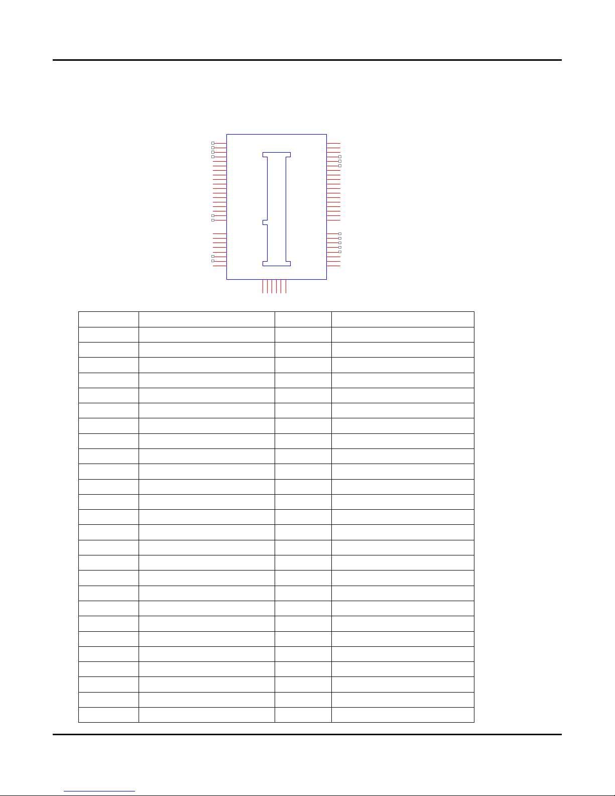
Pin
Signal
Pin
Signal
1
PCIE_WAKE#
2
3VSB
3
NC 4 GND
5
NC 6 +1.5V
7
MINICARD1_CLKREQ#
8
NC 9 GND
10
NC
11
PCIE_MCARD1_CLK_N
12
NC
13
PCIE_MCARD1_CLK_P
14
NC
15
GND
16
NC
17
NC
18
GND
19
NC
20
MINICARD0_DIS#
21
GND
22
PCIE_RST#
23
PCIE_MCARD1_RX_N
24
3VSB
25
PCIE_MCARD1_RX_P
26
GND
27
GND
28
+1.5V
29
GND
30
SMB_CLK
31
PCIE_MCARD1_TX_N
32
SMB_DATA
33
PCIE_MCARD1_TX_P
34
GND
35
GND
36
USB_9N
37
GND
38
USB_9P
39
3VSB
40
GND
41
3VSB
42
NC
43
GND
44
NC
45
NC
46
NC
47
NC
48
+1.5V
49
NC
50
GND
51
NC
52
3VSB
MINI PCIE CON
Ver:1.2
MINICA RD2
REV1
51
REV2
49
REV3
47
REV4
45
GND14
43
3.3VSB_5
41
3.3VSB_4
39
GND13
37
GND0
35
PETp0
33
PETn0
31
GND2
29
GND3
27
PERp0
25
PERn0
23
GND4
21
REV9/UIM_C4
19
REV10/UIM_C8
17
GND5
15
REFCLK+
13
REFCLK-
11
GND6
9
CLKREQ#
7
COEX2
5
COEX1
3
WAKE#
1
3.3VSB_2
52
GND7
50
1.5V_1
48
LED_WPAN#
46
LED_WLAN#
44
LED_WWAN#
42
GND8
40
USB_D+
38
USB_D-
36
GND9
34
SMBDAT
32
SMBCLK
30
1.5V_2
28
GND10
26
3.3VSB_1
24
PERST#
22
W_DISABLE#
20
GND11
18
UIM_VPP
16
UIM_RESET
14
UIM_CLK
12
UIM_DATA
10
UIM_PWR
8
1.5V_3
6
GND12
4
3.3VSB_3
2
MH1
MH1
MH2
MH2
MH3
MH3
MH4
MH4
MH5
MH5
MH6
MH6
2.19 Mini CARD Connector (Mini Card1)
A. Connector size: 2 X 26 = 52 Pin
B. Connector location: MINICARD2
C. Connector pin definition
2.0 Internal Connector Specification
User’s Manual Page 2-12
Page 25
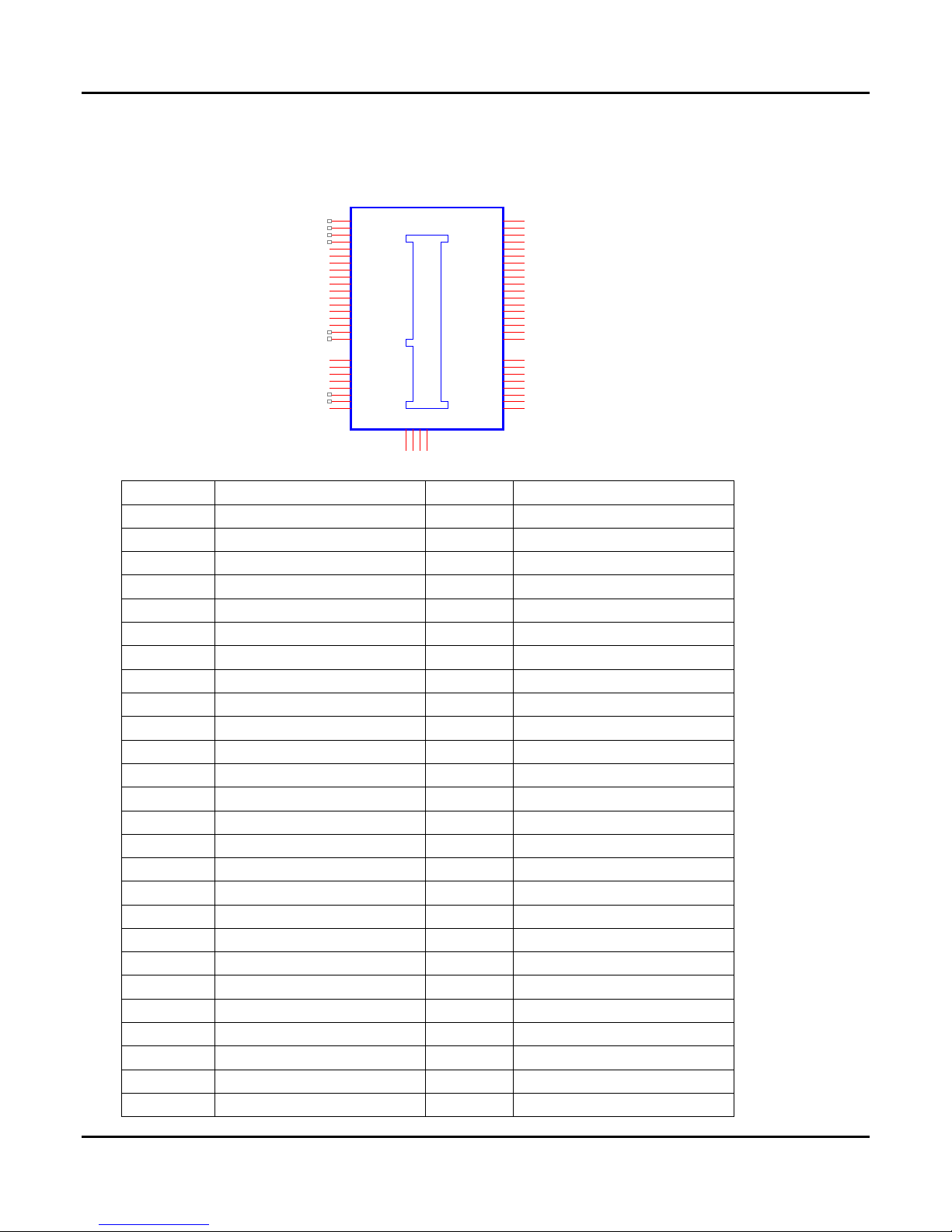
Pin
Signal
Pin
Signal
1
PCIE_WAKE#
2
3VSB
3
NC 4 GND
5
NC 6 +1.5V
7
MINICARD2_CLKREQ#
8
UIM_PWR
9
GND
10
UIM_DATA
11
PCIE_MCARD2_CLK_N
12
UIM_CLK
13
PCIE_MCARD2_CLK_P
14
UIM_RST
15
GND
16
UIM_VPP
17
NC
18
GND
19
NC
20
MINICARD0_DIS#
21
GND
22
PCIE_RST#
23
PCIE_MCARD2_RX_N
24
3VSB
25
PCIE_MCARD2_RX_P
26
GND
27
GND
28
+1.5V
29
GND
30
SMB_CLK
31
PCIE_MCARD2_TX_N
32
SMB_DATA
33
PCIE_MCARD2_TX_P
34
GND
35
GND
36
USB_10N
37
GND
38
USB_10P
39
3VSB
40
GND
41
3VSB
42
3.5G_LED_WWAN#
43
GND
44
3.5G_LED_WAN#
45
NC
46
3.5G_LED_WPAN#
47
NC
48
+1.5V
49
NC
50
GND
51
NC
52
3VSB
MINI PCIE CON
Ver:1.2
MINICA RD1
REV1
51
REV2
49
REV3
47
REV4
45
GND14
43
3.3VSB_5
41
3.3VSB_4
39
GND13
37
GND0
35
PETp0
33
PETn0
31
GND2
29
GND3
27
PERp0
25
PERn0
23
GND4
21
REV9/UIM_C4
19
REV10/UIM_C8
17
GND5
15
REFCLK+
13
REFCLK-
11
GND6
9
CLKREQ#
7
COEX2
5
COEX1
3
WAKE#
1
3.3VSB_2
52
GND7
50
1.5V_1
48
LED_WPAN#
46
LED_WLAN#
44
LED_WWAN#
42
GND8
40
USB_D+
38
USB_D-
36
GND9
34
SMBDAT
32
SMBCLK
30
1.5V_2
28
GND10
26
3.3VSB_1
24
PERST#
22
W_DISABLE#
20
GND11
18
UIM_VPP
16
UIM_RESET
14
UIM_CLK
12
UIM_DATA
10
UIM_PWR
8
1.5V_3
6
GND12
4
3.3VSB_3
2
H1
MH1
H2
MH2
H3
MH3
H4
MH4
2.20 MINI CARD Connector (Mini Card2)
A. Connector size: 2 X 26 = 52 Pin
B. Connector location: MINICARD1
C. Connector pin definition
2.0 Internal Connector Specification
User’s Manual Page 2-13
Page 26

3.0 External Connector Specification
3.0
EXTERNAL CONNECTOR
SPECIFICATION
User’s Manual
Page 27
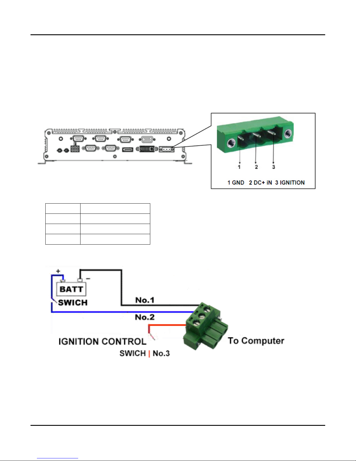
Pin
Signal
1
GND
2
DC_IN
3
IGNITION
3.0 EXTERNAL CONNECTOR SPECIFICATION
3.1 Power Input Connector
A. Connector size: 1 X 3 = 3 Pin
B. Connector location: PWR2
C. Connector pin definition
3.0 External Connector Specification
D. VBOX-3200's Power Wiring Diagram
User’s Manual Page 3-1
Page 28
Pin
Signal
Pin
Signal
1
GND
2
PWRBT#
3
PWRBT#
4
GND
A1
LEN_N
C1
LED_P
GPIO2
PHOENIX 3.5mm-F-90D
1
2
3
4
5
6
7
8
1
8
SW1
PUSH SW _LED _BR
1
1
3
3
2
2
4
4
A1
A1
C1
C1
MH1
MH1
MH2
MH2
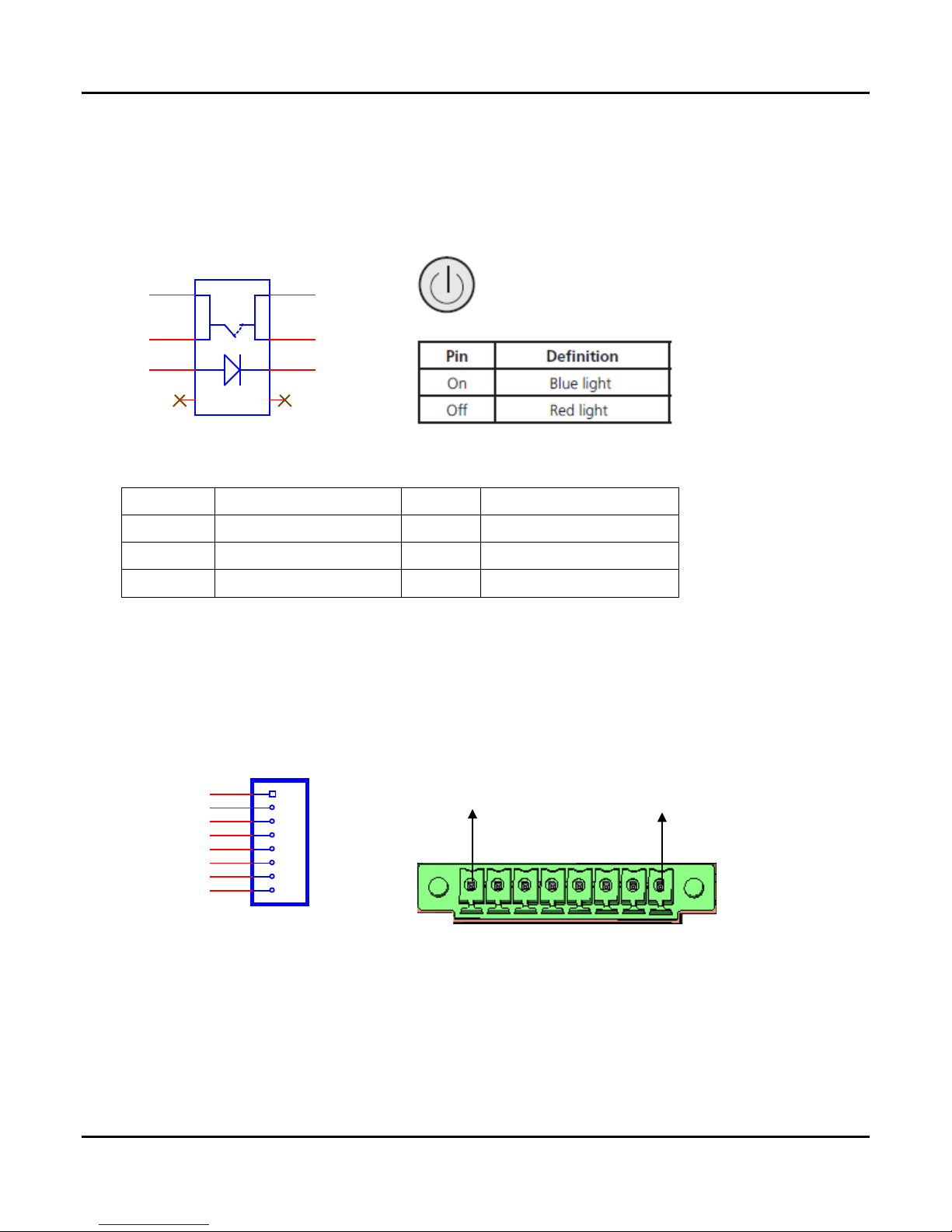
3.2 Power Button Connector
A. Connector size: 6 Pin
B. Connector location: SW1
C. Connector pin definition
3.0 External Connector Specification
3.3 DIO Connector
A. Connector size: 1 X 8 = 8 Pin
B. Connector location: GPIO2
User’s Manual Page 3-2
Page 29

Pin
Signal
1
+12V
2
GND
3
GPO1
4
GPO2
5
GPI1
6
GPI2
7
GPI3
8
GPI4
Pin
Signal
Pin
Signal
1
LAN0_MDI0P
2
LAN0_MDI0N
3
LAN0_MDI1P
4
LAN0_MDI2P
5
LAN0_MDI2N
6
LAN0_MDI1N
7
LAN0_MDI3P
8
LAN0_MDI3N
9
LAN0_ACT#
10
LAN0_ACTPW
11
LAN0_LINK#
12
LAN0_LINKPW
Green(R)
Orange(L)
LAN2
RJ45+LED-90
TD1+
1
TD3-
5
TD1-
2
TD2+
3
TD2-
6
MG2
H2
MG1
H1
L3
10
L4
9
L2
11
L1
12
TD3+
4
TD4+
7
TD4-
8
NH1
H3
NH2
H4
C. Connector pin definition
3.0 External Connector Specification
3.4 RJ45 Connector (LAN0)
A. Connector size: RJ45+LED
B. Connector location: LAN2
C. Connector pin definition
User’s Manual Page 3-3
Page 30
Pin
Signal
Pin
Signal
1
LAN1_MDI0P
2
LAN1_MDI0N
3
LAN1_MDI1P
4
LAN1_MDI2P
5
LAN1_MDI2N
6
LAN1_MDI1N
7
LAN1_MDI3P
8
LAN1_MDI3N
9
LAN1_ACT#
10
LAN1_ACTPW
11
LAN1_LINK#
12
LAN1_LINKPW
Pin
Signal
Pin
Signal
1
TD1+
2
TD1-
3
TD2+
4
TD3+
5
TD3-
6
TD2-
7
TD4+
8
TD4-
Green(R)
Orange(L)
LAN1
RJ45+LED-90
TD1+
1
TD3-
5
TD1-
2
TD2+
3
TD2-
6
MG2
H2
MG1
H1
L3
10
L4
9
L2
11
L1
12
TD3+
4
TD4+
7
TD4-
8
NH1
H3
NH2
H4
3.5 RJ45 Connector (LAN1)
A. Connector size: RJ45+LED
B. Connector location: LAN1
C. Connector pin definition
3.0 External Connector Specification
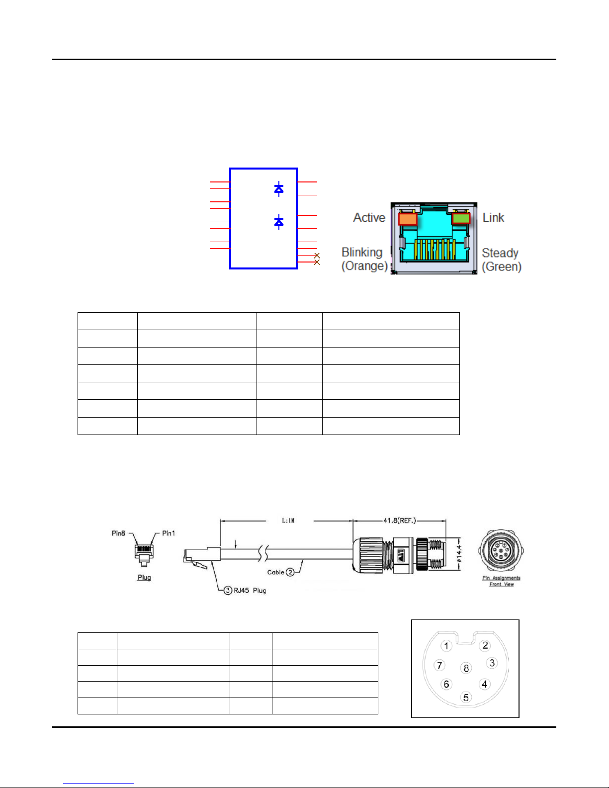
3.6 M12 Connecting to the Network
A. M12 to RJ45 Cable
B. M12 connector pin define
User’s Manual Page 3-4
Page 31
Pin
Signal
Pin
Signal
1
TD1+
2
TD1-
3
TD2+
4
TD3+
5
TD3-
6
TD2-
7
TD4+
8
TD4-
Pin
Signal
Pin
Signal
1
COM1_DCD
2
COM1_RXD
3
COM1_TXD
4
COM1_DTR
5
GND
6
COM1_DSR
7
COM1_RTS
8
COM1_CTS
9
COM1_RI/ +5V/+12V
COM5
COMP-M-90
5
9
4
8
3
7
2
6
1
H1
H2
9
6 1 5
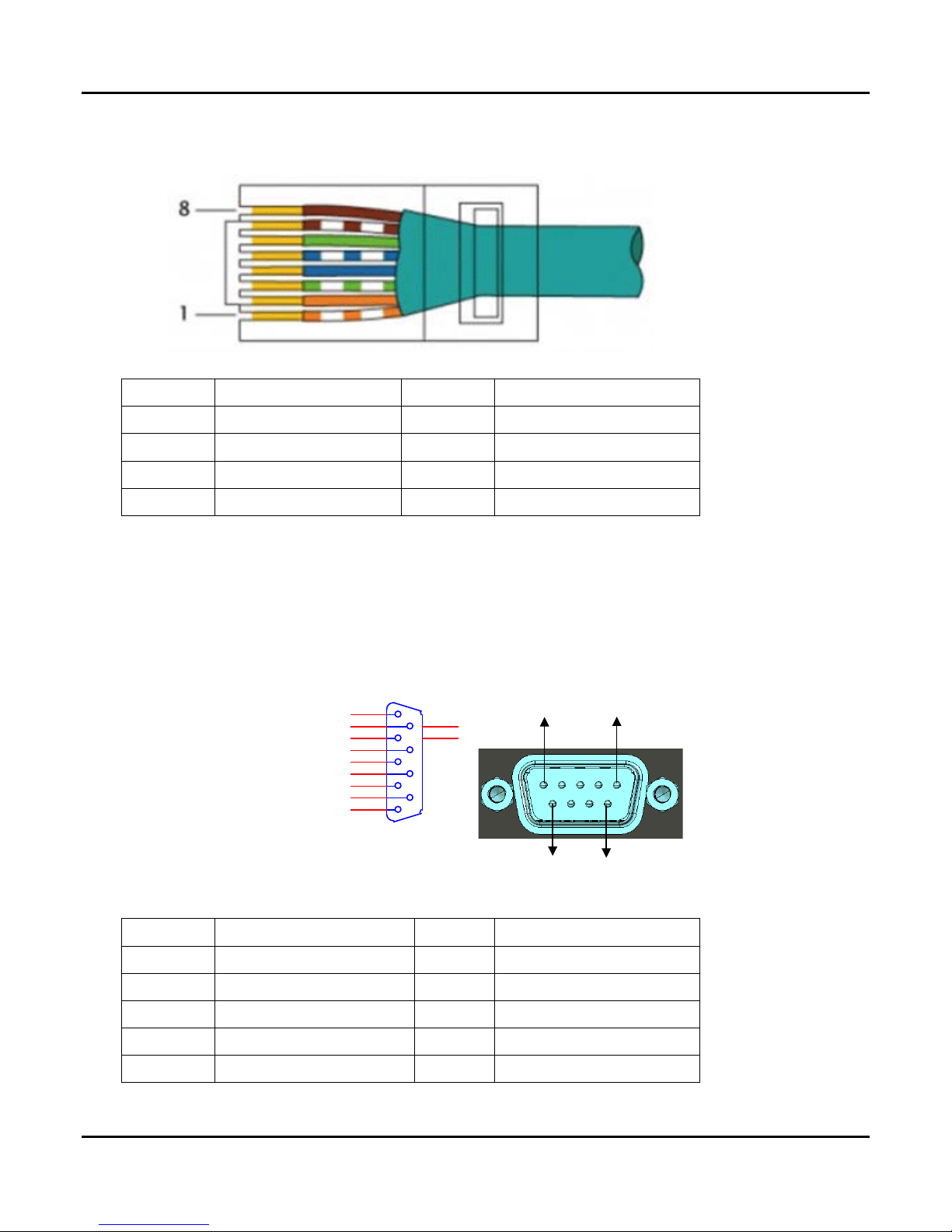
C. CAT5 connector pin define
3.0 External Connector Specification
3.7 COM Port Connector (COM1)
A. Connector size: DB9
B. Connector location: COM5
C. Connector pin definition (RS-232)
User’s Manual Page 3-5
Page 32
Pin
Signal
Pin
Signal
1
COM1_TXD-
2
COM1_TXD+
3
COM1_TXD+
4
COM1_RXD-
5
GND
6
NC 7 NC 8 NC 9 NC
Pin
Signal
Pin
Signal
1
COM1_TXD-/RXD-
2
COM1_TXD+/RXD+
3
NC 4 NC 5 GND
6
NC 7 NC 8 NC 9 NC
Analog RED
Analog GREEN
Analog BLUE
Analog HSync
Analog GroundAnalog Ground
TX2-
TX2+TX0+
TX0-
TX1-
TX1+
TX4-
TX4+
TX3-
TX3+
TX5-
TX5+
DDC CLK
DDC DATA
Analog VSync
2/4 Shield
HotPlugDet
TX Clk+
TX Clk-
Ground
+5V Power
TX Clk Shield
1/3 Shield
0/5 Shield
MGND
MGND
DVI-I CON-90
DVID2
8
7
6
5
4
3
2
1
9
10
11
12
13
14
15
16
17
18
19
20
21
22
23
24
C1
C2
C5
C4
C3
C6
H1
H2
H3
H4
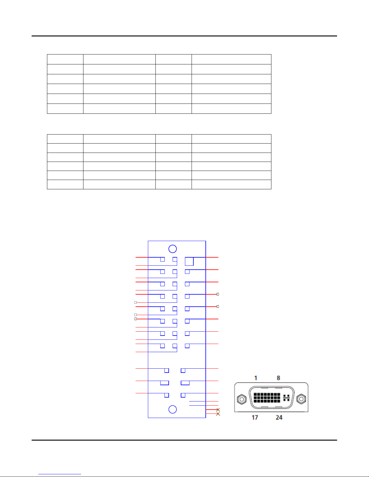
D. Connector pin definition (RS-422)
E. Connector pin definition (RS-485)
3.0 External Connector Specification
3.8 DVI-I Connector (DP1+VGA)
A. Connector size: DVI-I
B. Connector location: DVID2
User’s Manual Page 3-6
Page 33

Pin
Signal
Pin
Signal
1
DVI_TX2_N
2
DVI_TX2_P
3
GND
4
5VSB_USB
5
+12V_PWR
6
DVI_DDC_CLK
7
DVI_DDC_DATA
8
CRT_VSYNC
9
DVI_TX1_N
10
DVI_TX1_P
11
GND
12
USB_12N
13
USB_12P
14
+5V_DVI_PWR
15
GND
16
DVI_HPD
17
DVI_TX0_N
18
DVI_TX0_P
19
GND
20
CRT_DAC_SDA
21
CRT_DAC_SCL
22
NC
23
DVI_CLK_P
24
DVI_CLK_N
C1
CRT_RED
C2
CRT_GREEN
C3
CRT_BLUE
C4
CRT_HSYNC
C5
GND
C6
GND
Pin
Signal
Pin
Signal
1
5VSB_USB
2
USB0_N
3
USB0_P
4
GND
5
5VSB_USB
6
USB1_N
7
USB1_P
8
GND
USB2
2USB-F-90
VCC
1
DATA1+
3
DATA1-
2
GND
4
VCC
5
GND
8
DATA-
6
DATA+
7
MGND
9
MGND
10
MGND
11
MGND
12
C. Connector pin definition
3.0 External Connector Specification
3.9 USB Connector (USB 0/1)
A. Connector size: USB TYPEA
B. Connector location: USB2
C. Connector pin definition
User’s Manual Page 3-7
Page 34
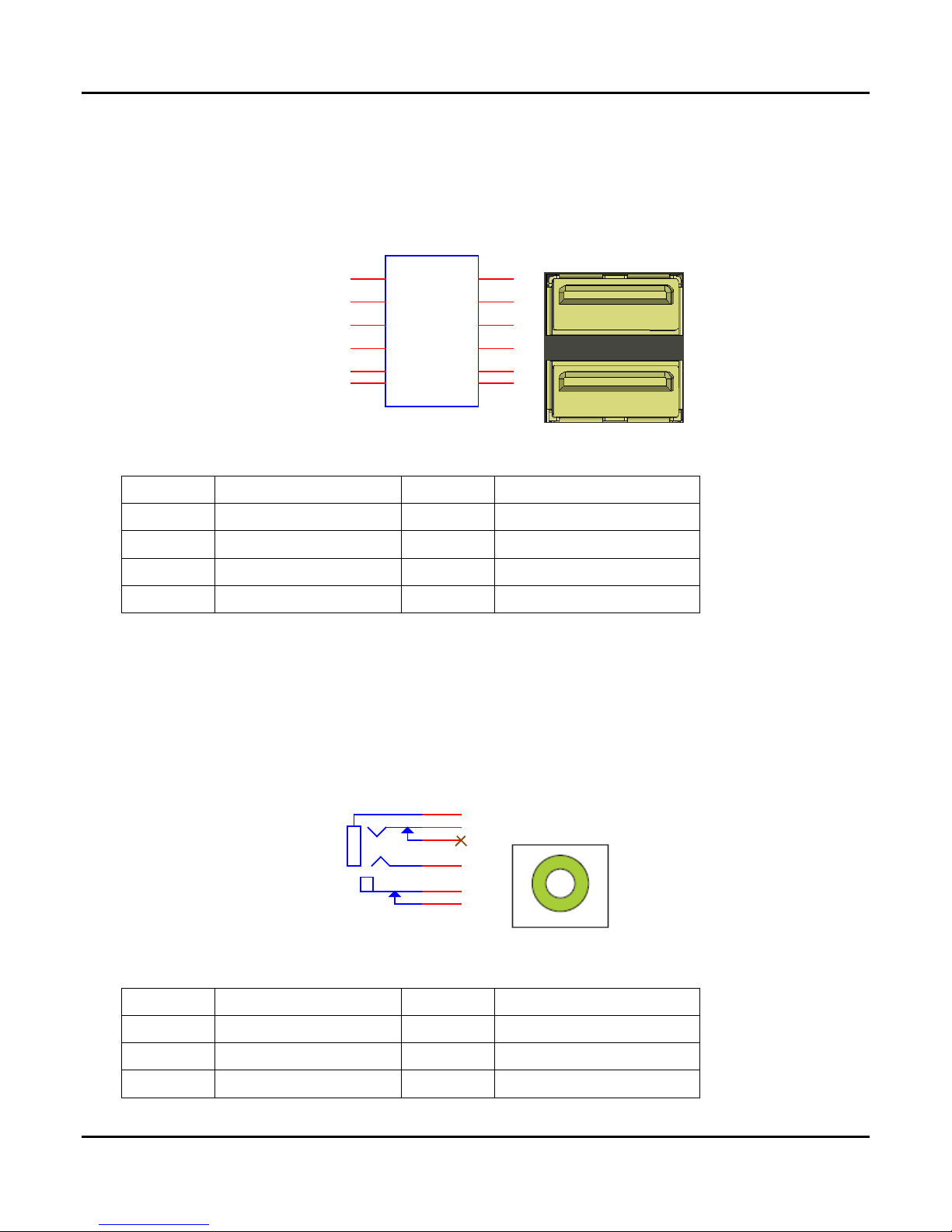
Pin
Signal
Pin
Signal
1
5VSB_USB
2
USB2_N
3
USB2_P
4
GND
5
5VSB_USB
6
USB3_N
7
USB3_P
8
GND
Pin
Signal
Pin
Signal
1
FRONT_OUT_L
2
FRONT-JD
3
NC 4 FRONT_OUT_R
5
GND
6
GND
USB1
2USB-F-90
VCC
1
DATA1+
3
DATA1-
2
GND
4
VCC
5
GND
8
DATA-
6
DATA+
7
MGND
9
MGND
10
MGND
11
MGND
12
LOUT1
AUDIO_PHONE-F-90
3
4
5
1
6
2
3.10 USB Connector (USB2/3)
A. Connector size: USB TYPEA
B. Connector location: USB1
C. Connector pin definition
3.0 External Connector Specification
3.11 Audio Connector
A. Connector size: Phone Jack
B. Connector location: Audio2
C. Connector pin definition
User’s Manual Page 3-8
Page 35
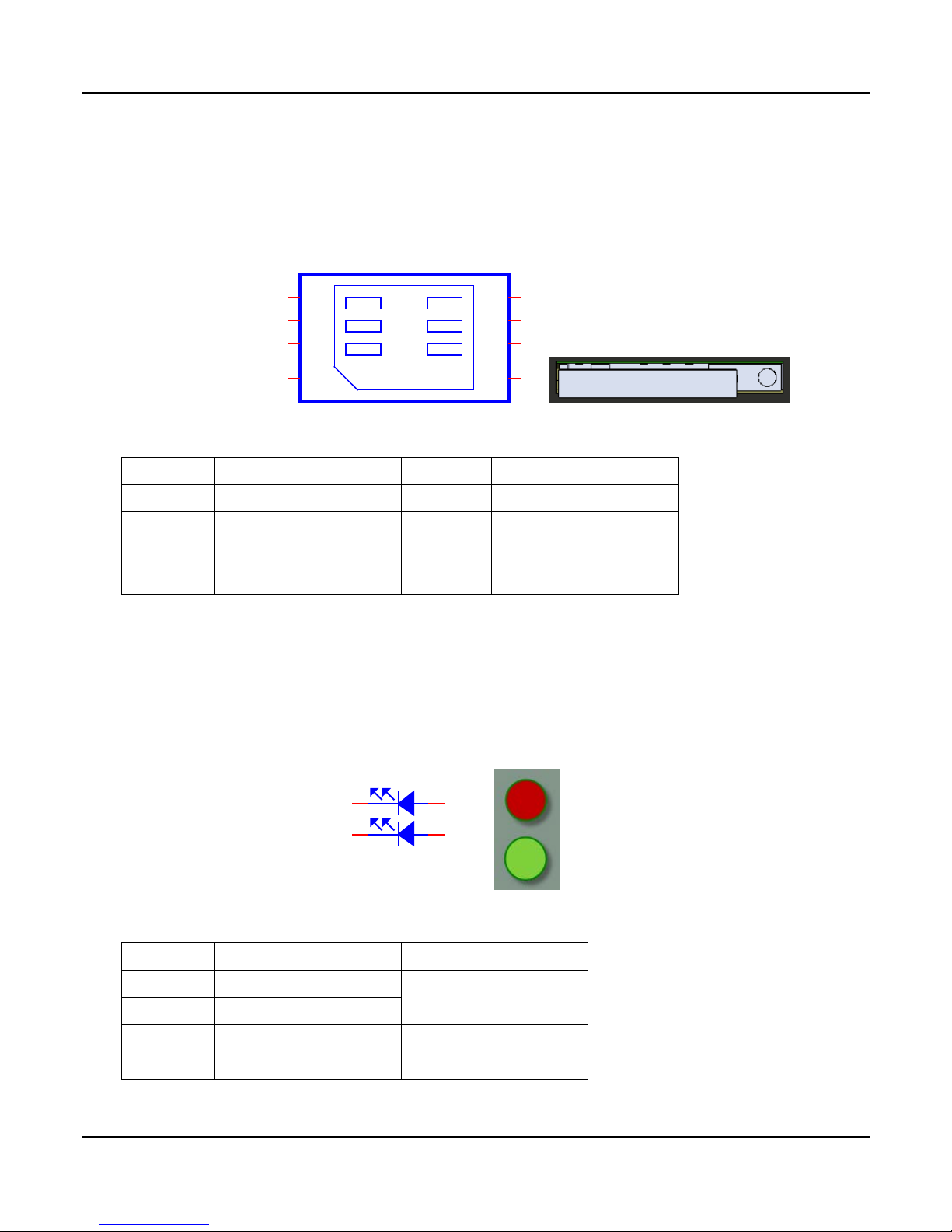
Pin
Signal
Pin
Signal
C1
VCC
C5
GND
C2
RST
C6
VPP
C3
CLK
C7
DATA
SW1
GND
SW2
GND
Pin
Signal
Location
A1
3.5G_LED_P
C1
3.5G_LED_N
A2
UPS_LED_P
C2
UPS_LED_N
SIM1
VCC
C1
RST
C2
CLK
C3
I/O
VPP
GND
SW2
SW1
SW
上
下
LED1
LED_RG
HOUSING
A2C2
A1C1
3.12 CAN Pin Assignment
A. Connector size: 6 Pin
B. Connector location: SIM1
C. Connector pin definition
3.0 External Connector Specification
3.13 UPS/3.5G LED
A. Connector size: 2 Layer LED with Housing
B. Connector location: LED1
C. Connector pin definition
Down
UP
User’s Manual Page 3-9
Page 36
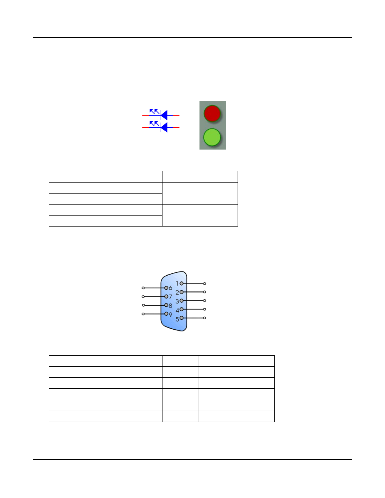
Pin
Signal
Location
A1
ACC_LED_P
C1
ACC_LED_N
A2
HDD_LED_P
C2
HDD_LED_N
Pin
Signal
Pin
Signal
1
nc 6 CAN_GND
2
CAN_L
7
CAN_H
3
CAN_GND
8
nc
4
nc 9 nc
5
nc
上
下
LED2
LED_RG
HOUSING
A2
A1
3.14 HDD/ACC LED
A. Connector size: 2 Layer LED with Housing
B. Connector location: LED2
C. Connector pin definition
3.0 External Connector Specification
Down
3.15 CAN BUS Pin Assignment
A. Connector pin definition
UP
User’s Manual Page 3-10
Page 37

4.0 System Installation
4.0
SYSTEM INSTALLATION
User’s Manual
Page 38
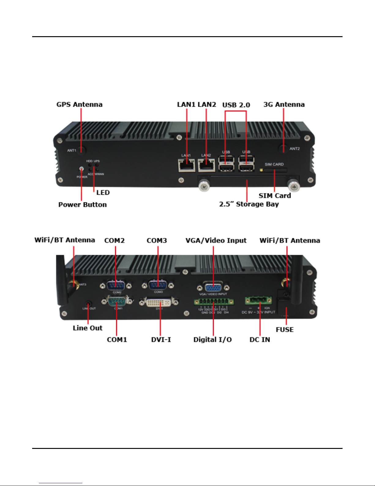
4.0 SYSTEM INSTALLATION
4.1 System Introduction
4.0 System Installation
User’s Manual Page 4-1
Page 39
4.0 System Installation
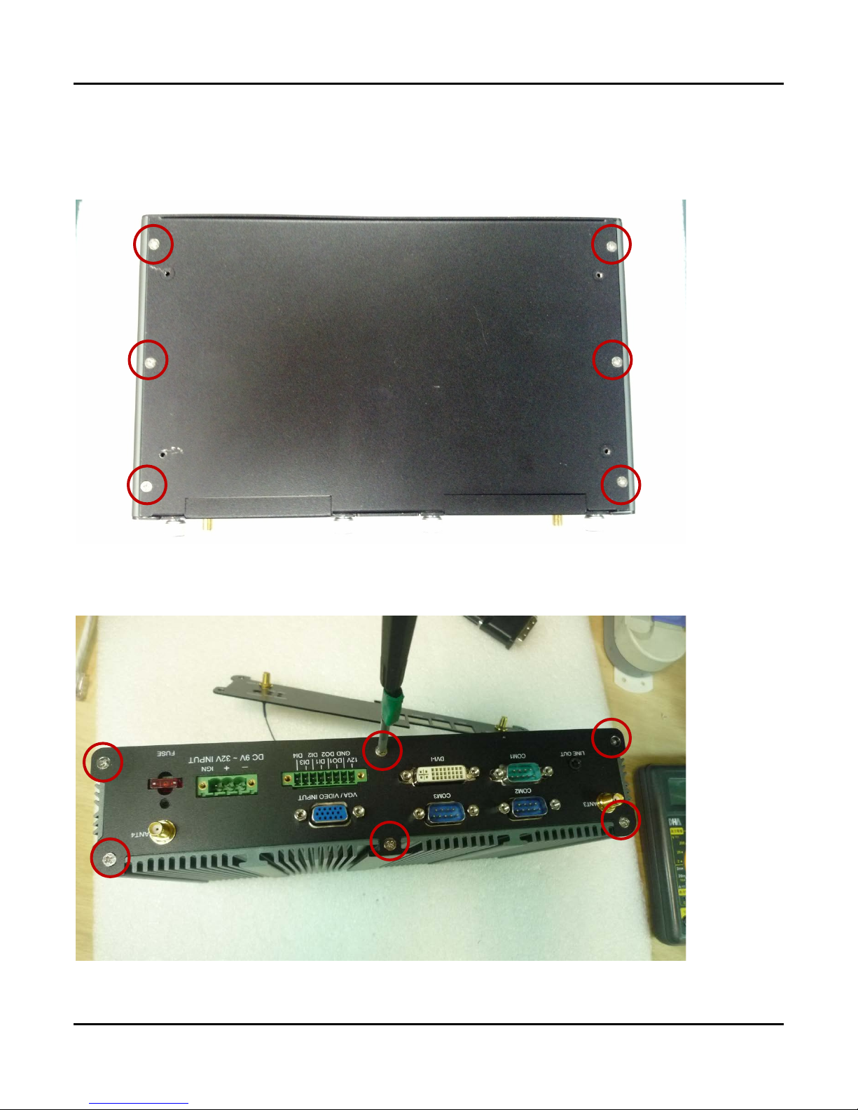
4.2 Opening Chassis
Step1. Unscrew the six screws of the Back Cover as shown in the picture.
Step2. Unscrew the six screws of the Front Panel as shown in the picture.
User’s Manual Page 4-2
Page 40
4.0 System Installation
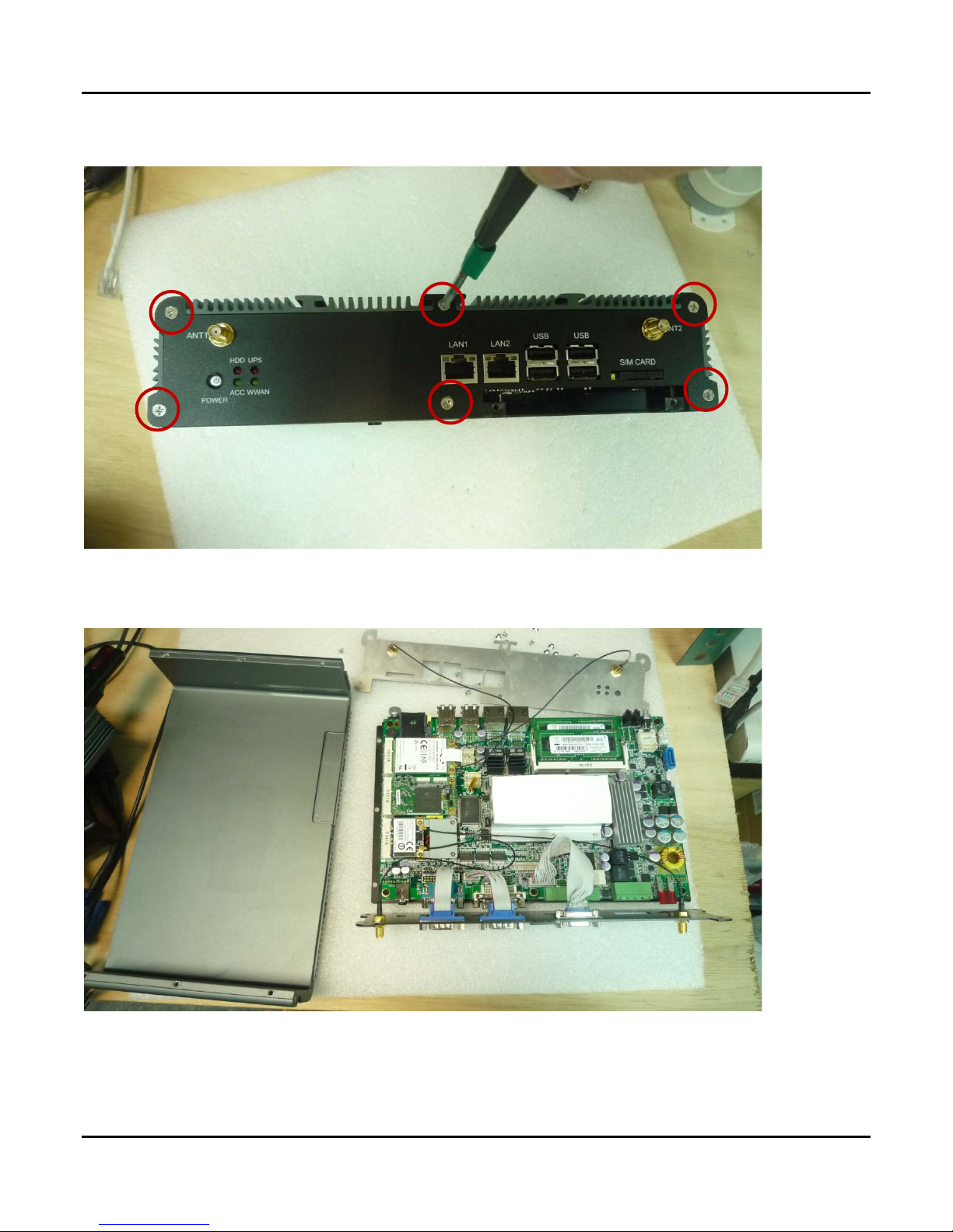
Step3. Unscrew the six screws of the Rear Panel as shown in the picture.
Step4. Open Top Cover as shown in the picture.
User’s Manual Page 4-3
Page 41
COM2 COM3 VGA
4.0 System Installation
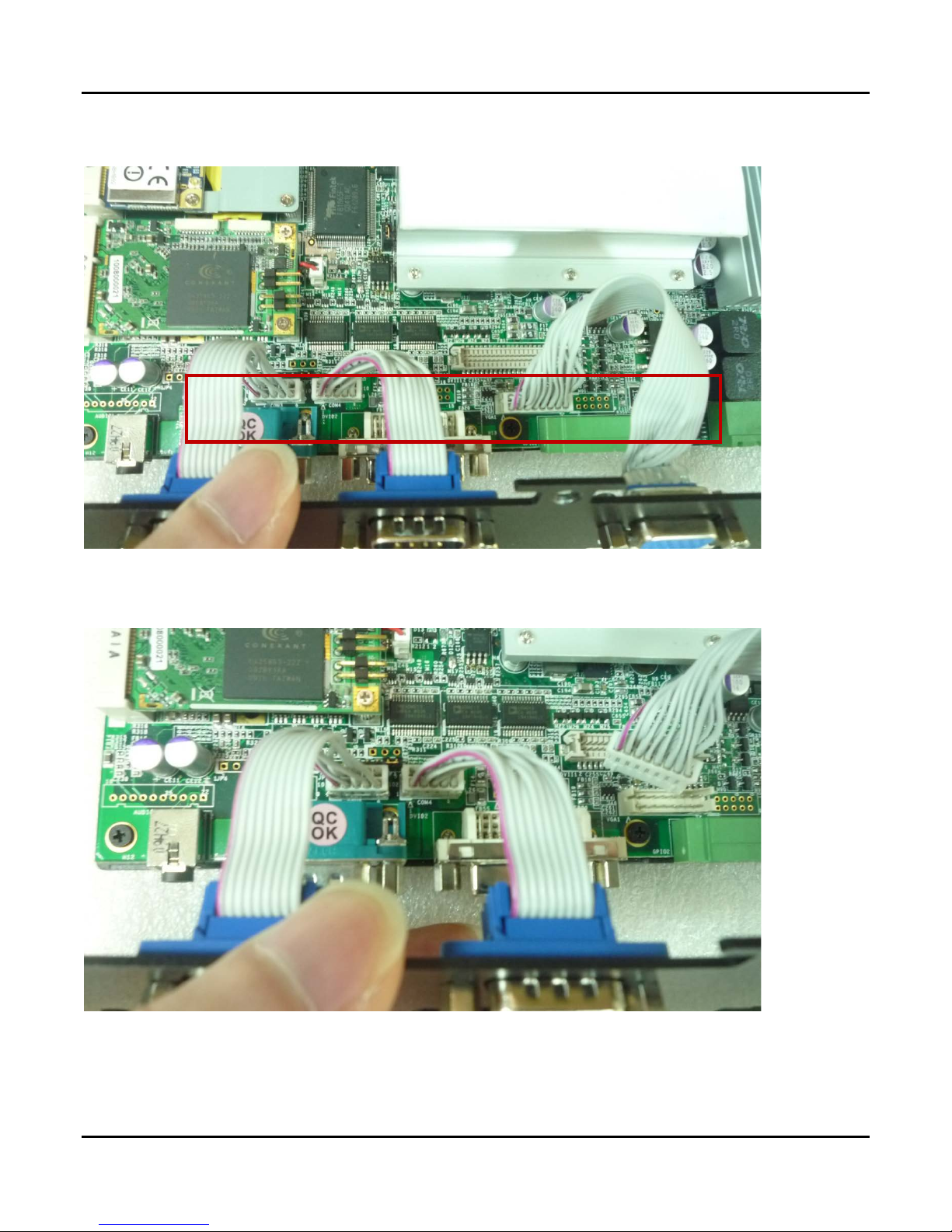
Step5. You can see three connectors connect with mainboard as shown in the picture.
Step6. Pull up the connector as shown in the picture.
User’s Manual Page 4-4
Page 42
4.0 System Installation
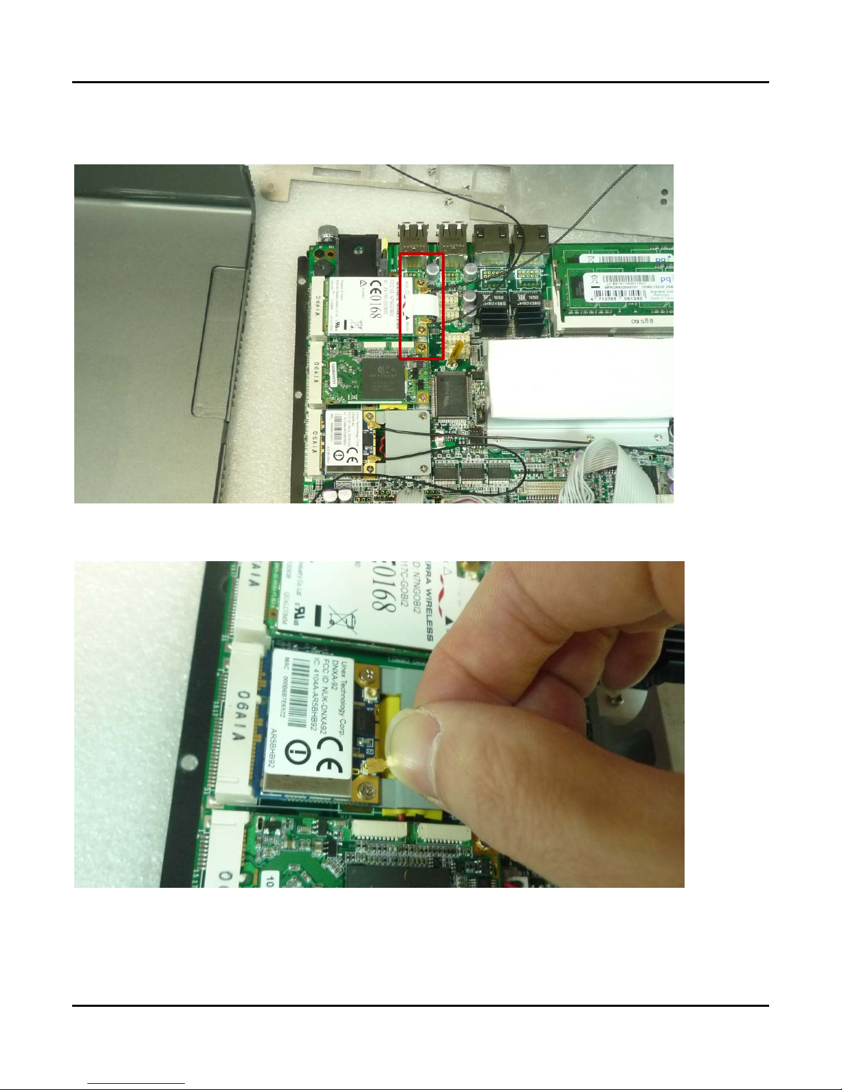
Step7. You can see Ipexs on the Mini PCIe module connectors as shown in the picture.
Step8. Pull up the Ipexs as shown in the picture.
User’s Manual Page 4-5
Page 43
4.3 Installing Memory
Step 1. Put Memory on this place as shown in the picture.
4.0 System Installation
Step 2. Hold the Memory with its notch aligned with the Memory socket of the board
and insert it at a 30-degreeangle into the socket as shown in the picture.
User’s Manual Page 4-6
Page 44
4.0 System Installation
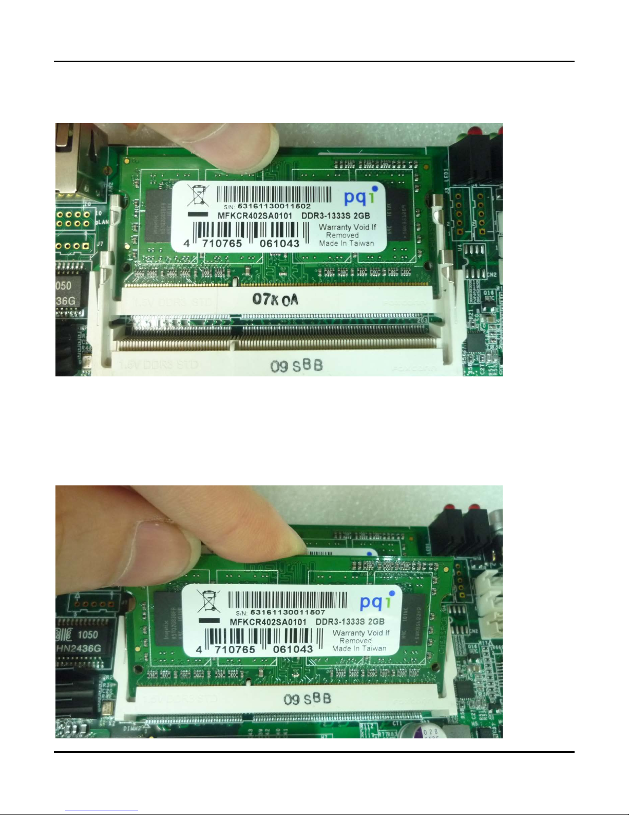
Step 3. Fully insert the module into the socket until a “click” is heard as shown in the
picture.
Step 4. Press down on the Memory so that the tabs of the socket lock on both sides of
the module.
Step 5. Hold the Memory with its notch aligned with the Memory socket of the board
and insert it at a 30-degreeangle into the socket as shown in the picture.
User’s Manual Page 4-7
Page 45
4.0 System Installation
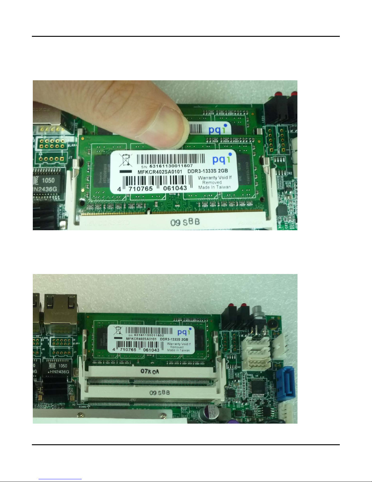
Step 6. Fully insert the module into the socket until a “click” is heard as shown in the
picture.
Step 7. Press down on the Memory so that the tabs of the socket lock on both sides of
the module as shown in the picture.
User’s Manual Page 4-8
Page 46
4.0 System Installation
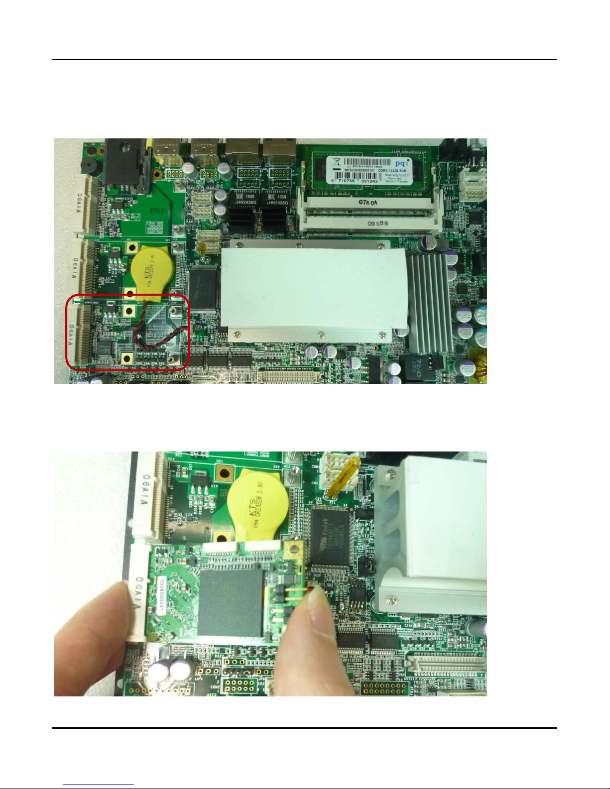
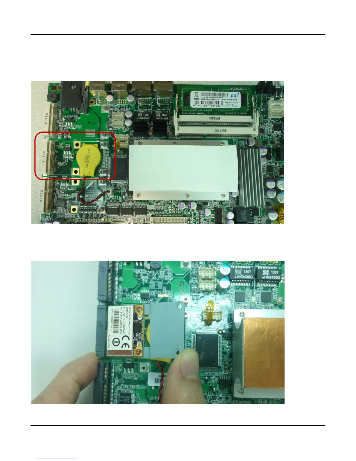
4.4 Installing MINI PCIe Expansion Card (PCIe 1)
Step 1. Put MINI PCIe Expansion Card on this place as shown in the picture.
Step 2. Hold the Module with its notch aligned with the socket of the board and insert it
at a 30 degree angle into the socket as shown in the picture.
User’s Manual Page 4-9
Page 47
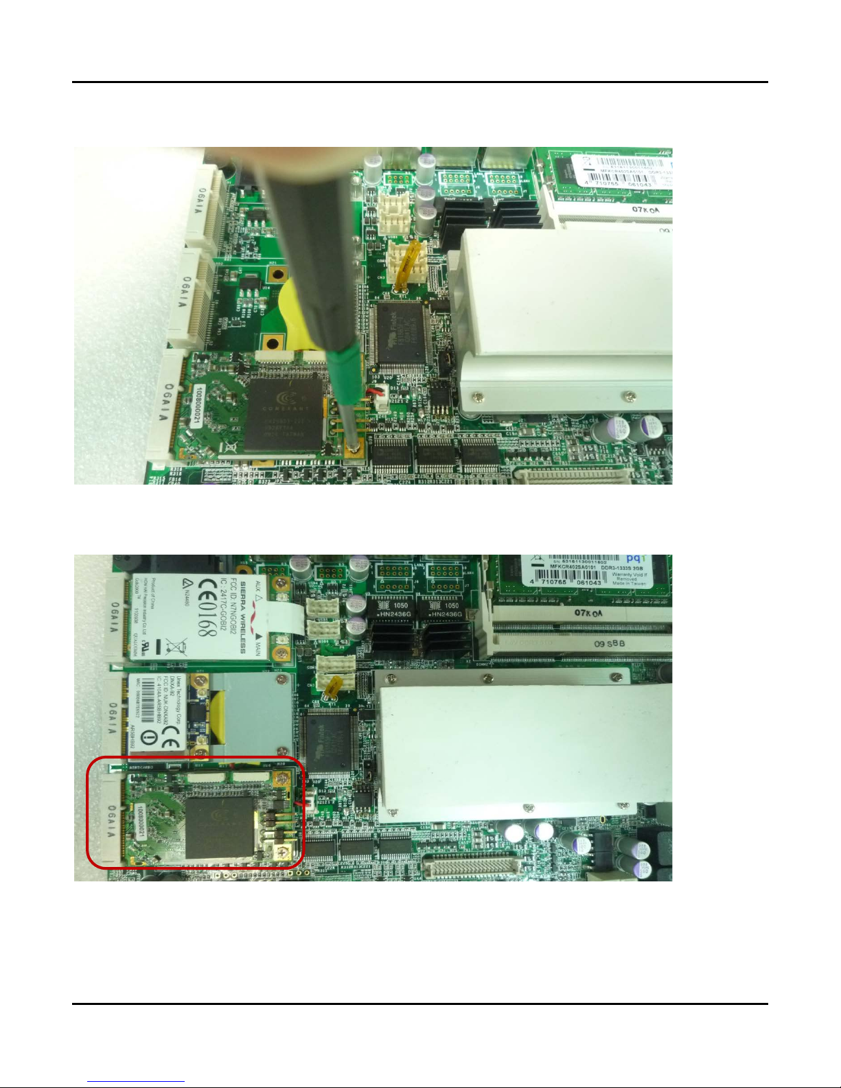
Step 3. Screw two screws to the holder as shown in the picture.
4.0 System Installation
Step 4. Done as shown in the picture.
User’s Manual Page 4-10
Page 48
4.0 System Installation
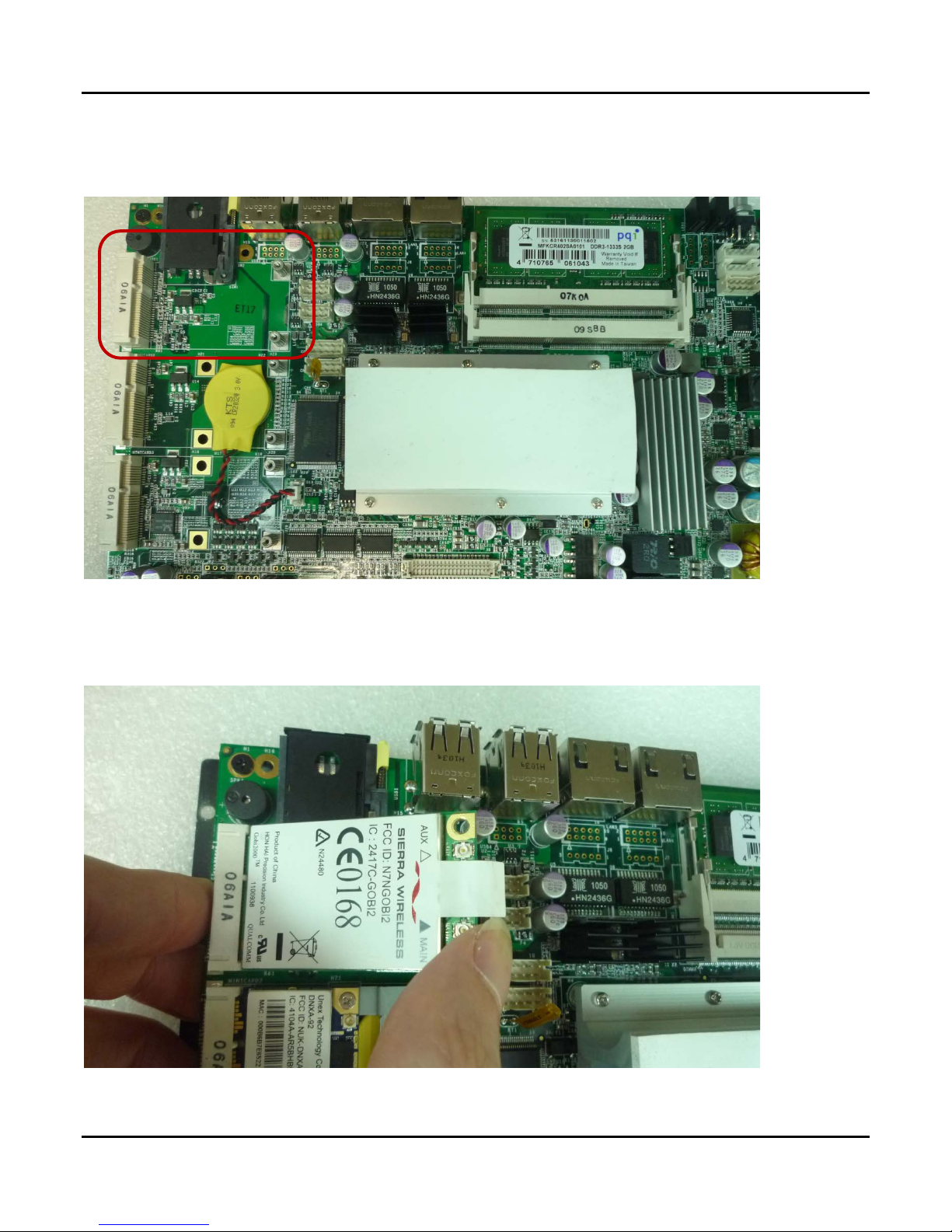
4.5 Installing MINI PCIe Expansion Card (PCIe 2, Wifi Module)
Step 1. Put MINI PCIe Expansion Card on this place as shown in the picture.
Step 2. Hold the Module with its notch aligned with the socket of the board and insert it
at a 30 degree angle into the socket as shown in the picture.
User’s Manual Page 4-11
Page 49
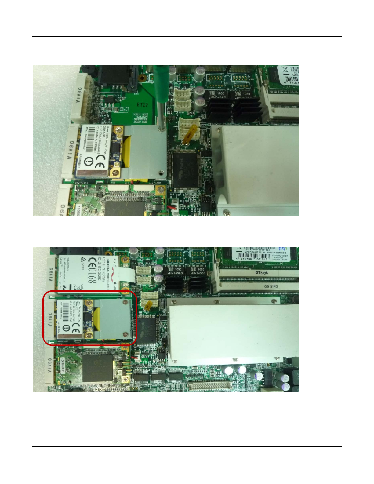
Step 3. Screw two screws to the holder as shown in the picture.
4.0 System Installation
Step 4. Done as shown in the picture.
User’s Manual Page 4-12
Page 50
4.0 System Installation
4.6 Installing MINI PCIe Expansion Card (PCIe 3, 3G Module only)
Step 1. Put MINI PCIe Expansion Card on this place as shown in the picture.
Step 2. Hold the Module with its notch aligned with the socket of the board and insert it
at a 30 degree angle into the socket as shown in the picture.
User’s Manual Page 4-13
Page 51
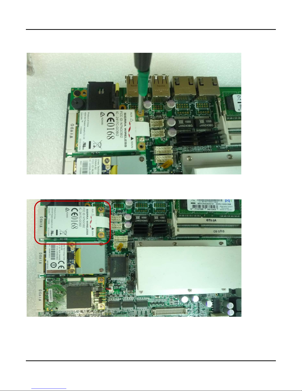
Step 3. Screw two screws to the holder as shown in the picture.
4.0 System Installation
Step 4. Done as shown in the picture.
User’s Manual Page 4-14
Page 52
4.0 System Installation
4.7 Installing Internal Antenna Cable
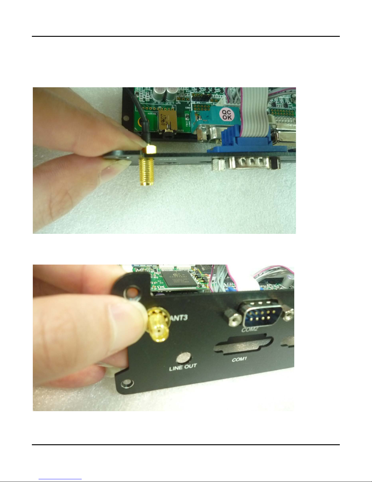
Step 1. Take the SMA Connector and Plug into IO Panel as shown in the picture.
Step 2. Put the Washer into the SMA Connector as shown in the picture.
User’s Manual Page 4-15
Page 53
4.0 System Installation
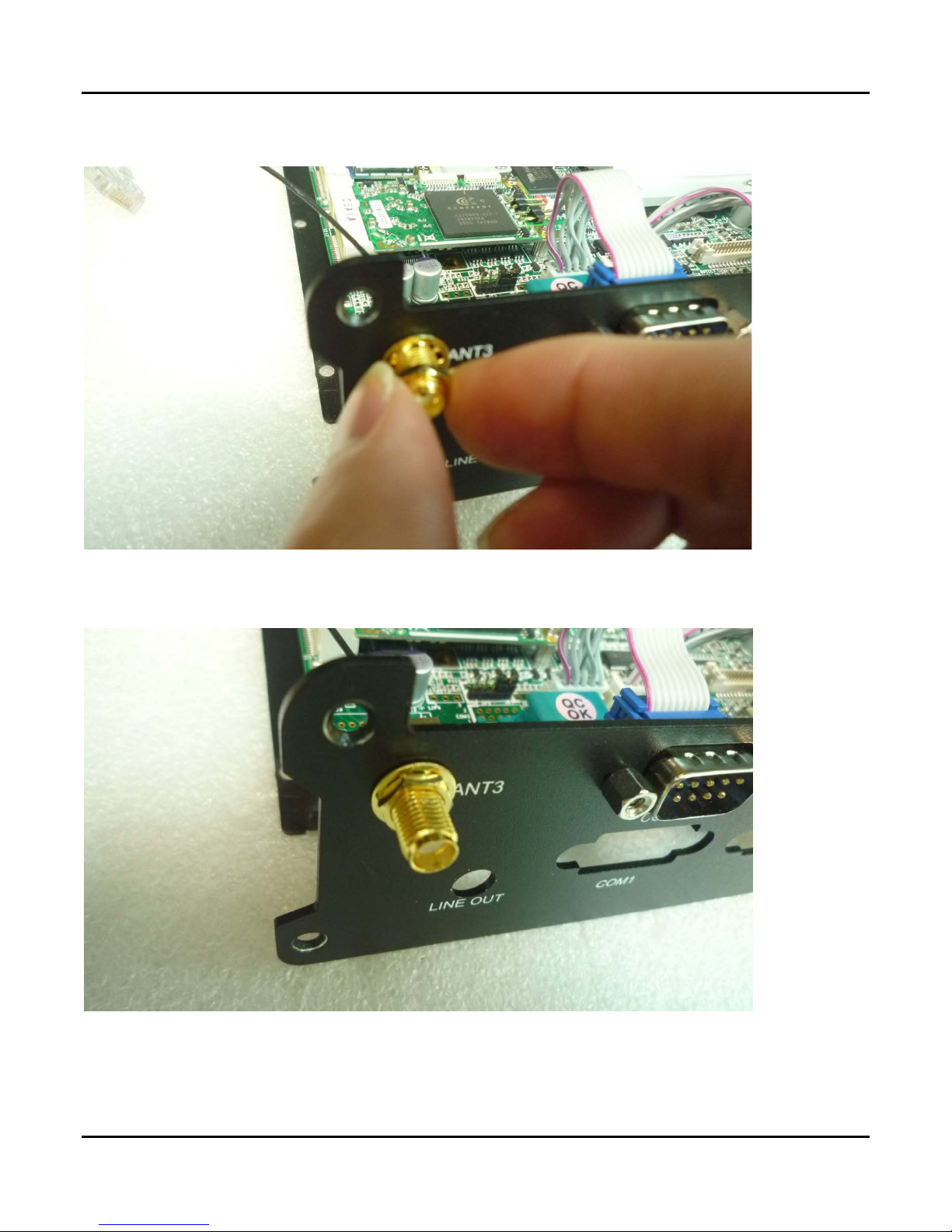
Step 3. Put the Oring to SMA Connector and tighten as shown in the picture.
Step 4. Done as shown in the picture.
User’s Manual Page 4-16
Page 54
4.0 System Installation
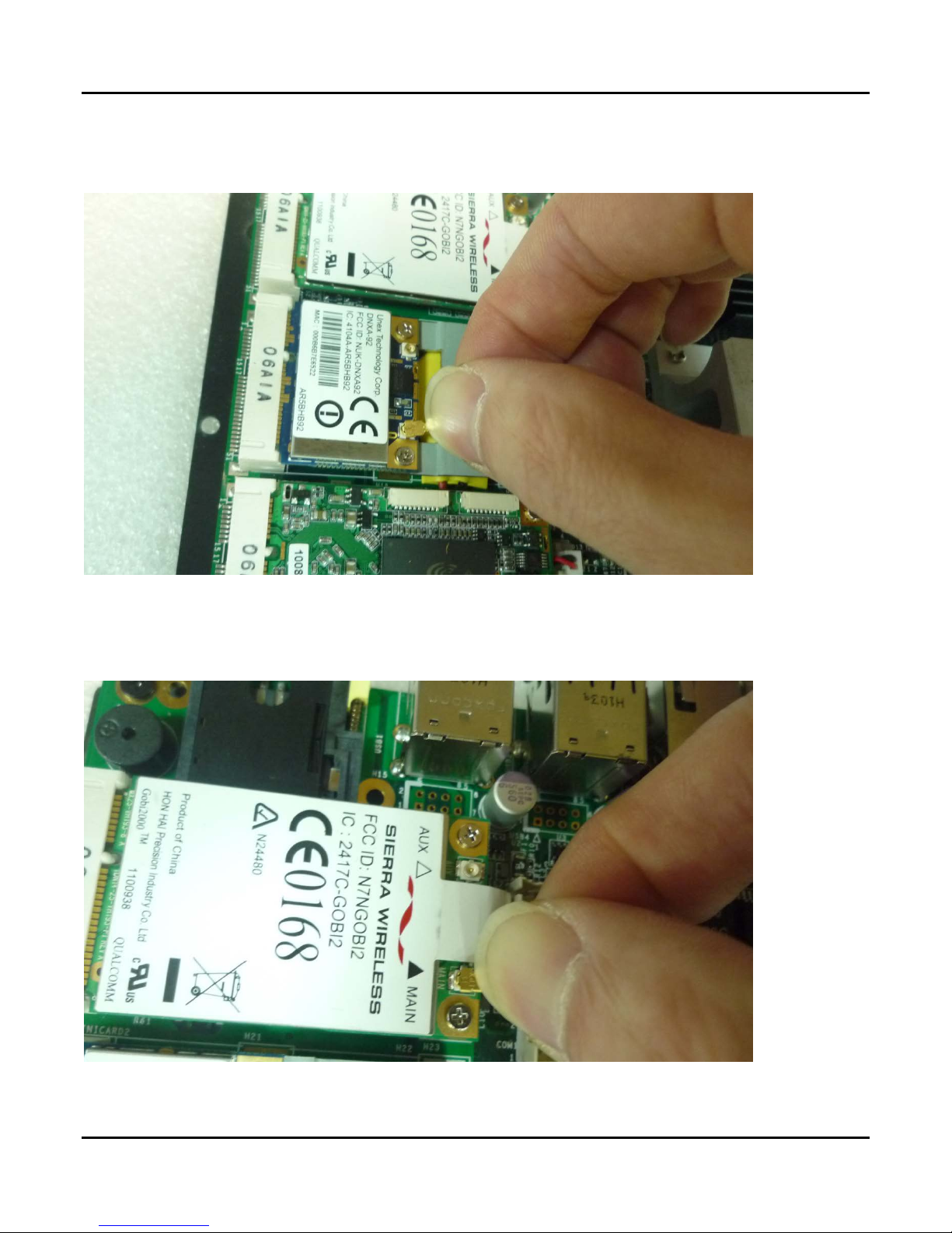
Step 5. Take the Ipex Connector and press on the wifi module asshown in the
picture.(Wifi)
Step 6. Take the Ipex Connector and press on the 3G module as shown in the picture.
(3G)
User’s Manual Page 4-17
Page 55

4.0 System Installation
Step 7. Take the Ipex Connector and press on the GPS module as shown in the picture.
(GPS, only support passive Antenna)
User’s Manual Page 4-18
Page 56
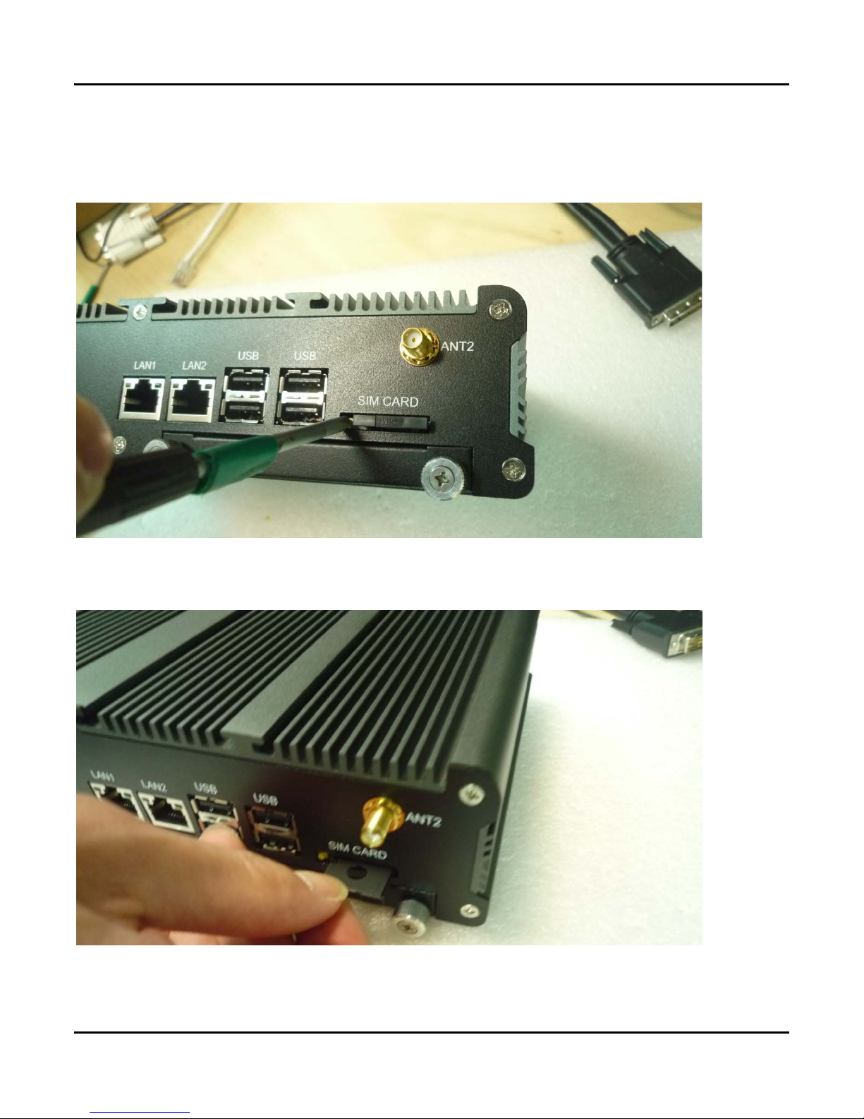
4.8 Installing SIM Card
Step 1. Use thin stick to push the button as shown in the picture.
4.0 System Installation
Step 2. Take the holder away from front panel as shown in the picture.
User’s Manual Page 4-19
Page 57
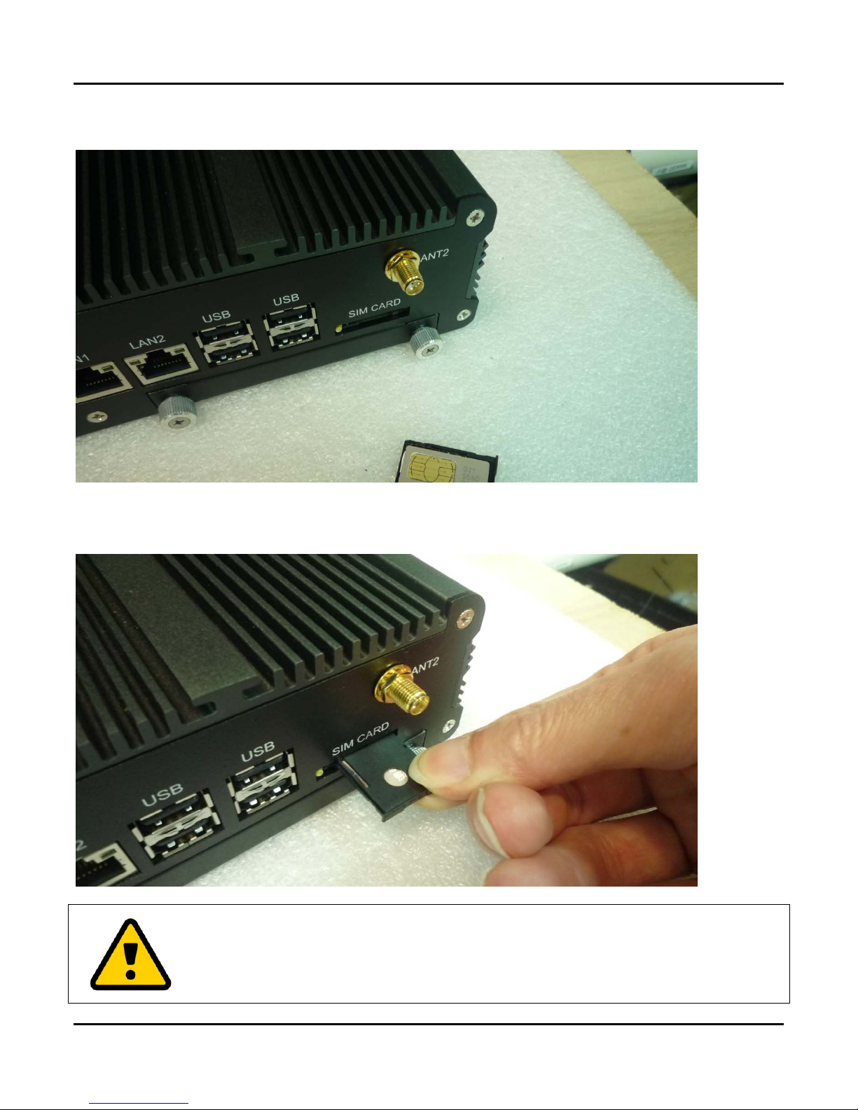
Step 3. Put your SIM Card into the holder as shown in the picture.
4.0 System Installation
Step 4. Take the SIM card holder and Insert it into the socket as shown in the picture.
Attention:
Please cut the main power when you insert the SIM.
Caution :
The SIM card will be not detected.
User’s Manual Page 4-20
Page 58
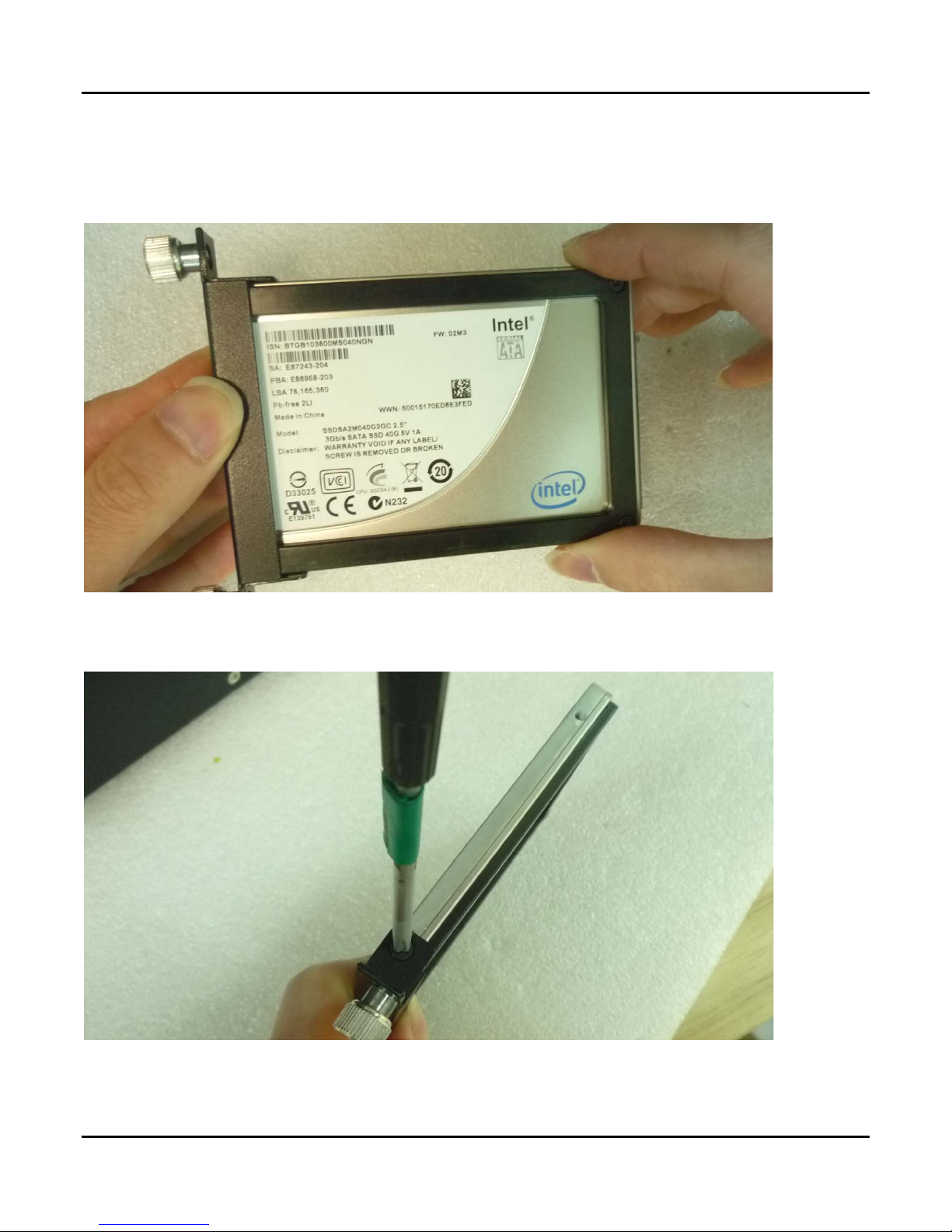
4.9 Installing HDD
Step 1. Put the HDD into HDD Holder as shown in the picture.
4.0 System Installation
Step 2. Screw two screws on both side as shown in the picture.
User’s Manual Page 4-21
Page 59
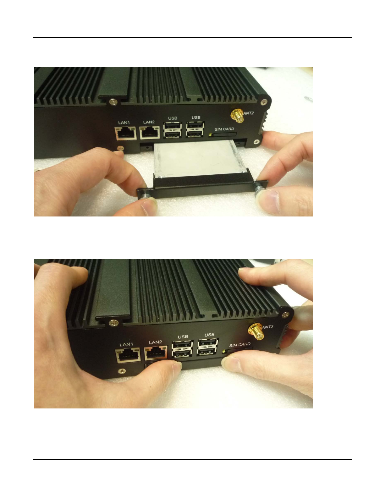
Step 3. Push the HDD Holder into the socket as shown in the picture.
4.0 System Installation
Step 4. Fully insert the HDD Holder into the socket until a “click” is heard
as shown in the picture.
User’s Manual Page 4-22
Page 60
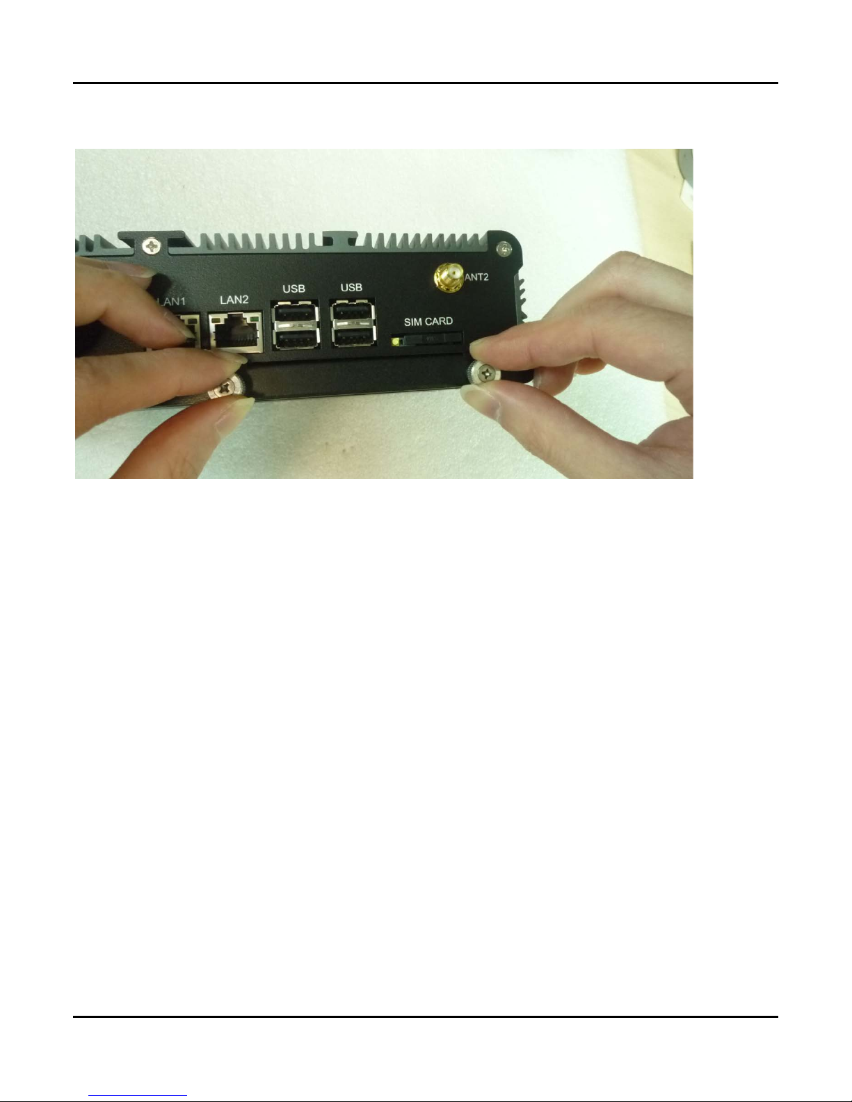
Step 5. Tighten to Storage Bracket screws as shown in the picture.
4.0 System Installation
User’s Manual Page 4-23
Page 61

5.0 System Resource
5.0
SYSTEM RESOURCE
User’s Manual
Page 62
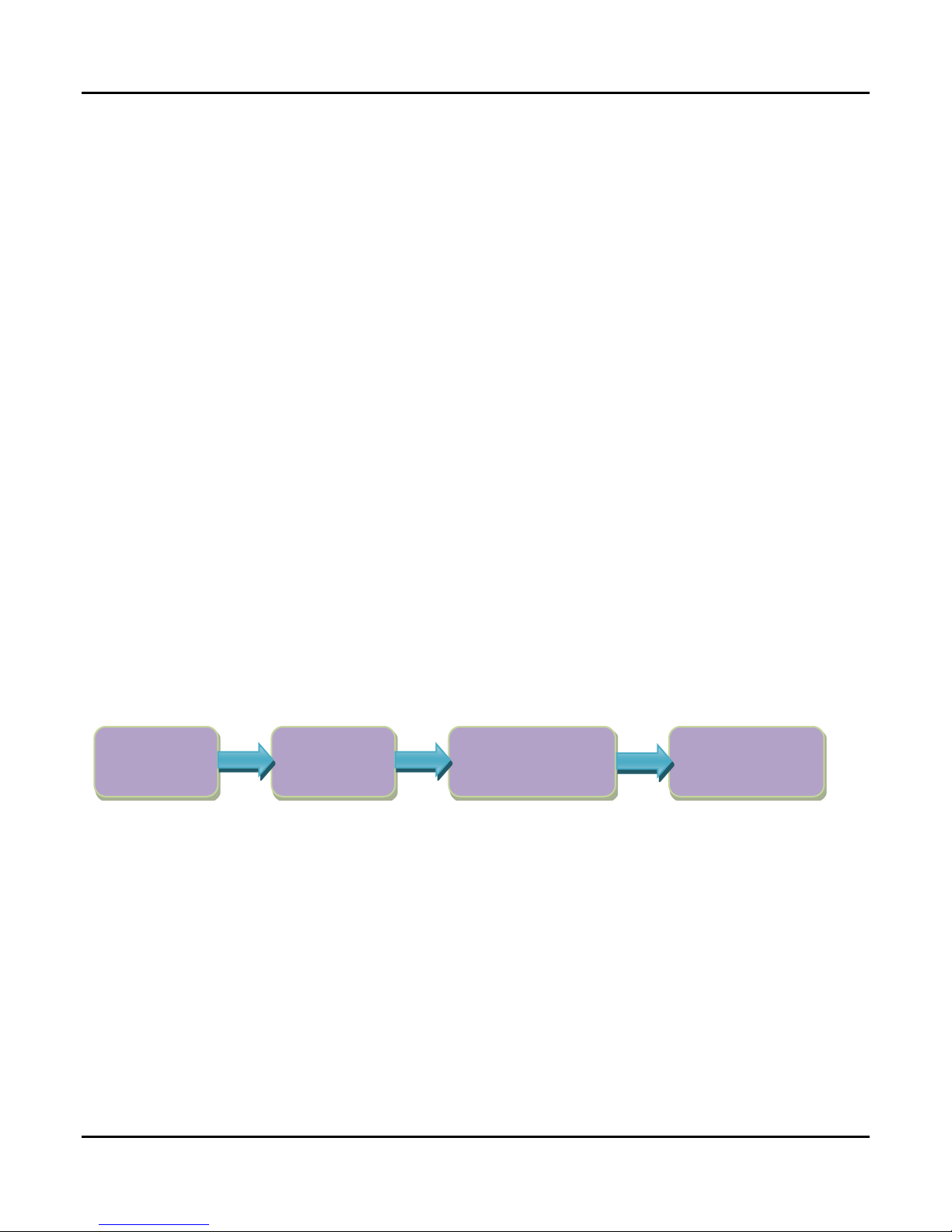
12V or 24V
Check IGN
IGN on (High)
System Turn
5.0 System Resource
5.0 SYSTEM RESOURCE
5.1 Ignition Power Management Quick Guide
Startup/shutdown conditions from the IGNITION signal:
IGNITION startup signal must be valid during 5 sec. (anti noise protection).
IGNITION shutdown – IGNITION signal must be inactive during 5 minutes, then PIC
controller initiate Power Button signal (OS must be set to shutdown from the
Power Button). It generate Main Button shutdown event and then goes to
complete power off.
Typically the system can start only from IGNITION signal, because startup PIC controller
is disconnected from the power source.
The system can be switched off from:
Power IGNITION OFF signal.
ACPI OS shutdown
Power Button – generate ACPI event (OS dependent).
Power
Status
more than 5sec
Power Ignition Startup Procedure
on
User’s Manual Page 5-1
Page 63
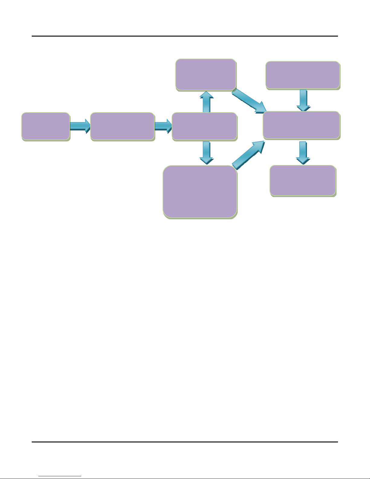
Check Delay
Time
IGN off (Low)
Check IGN
Status
5 sec later
Shutdown from OS
Delay Time Off
OS Shutdown
System
Delay Time On
More than 10 sec
Power Management
Delay 5 Sec
A. Delay 2 Hours
B. Delay 4 Hours
C. Delay 12 Hours
Power Ignition Shutdown Procedure
5.0 System Resource
& IGN off
System Power off
Power-off delay time is selectable by BIOS to disable and enable in 5 min / 2hr / 4hr
/ 12hr
Ignition On/Off status detectable by SW
If the ignition is off and the system is still on after 5 minutes, VBOX-3200 will shut
down automatically.
If the ignition is turned on again and the power-off delay is in progress, VBOX-3200
will cancel the delay function and will continue to operate normally.
If the ignition is turned on again and the power-off delay ended, VBOX-3200 will
shut down completely will power-on again automatically.
User’s Manual Page 5-2
Page 64
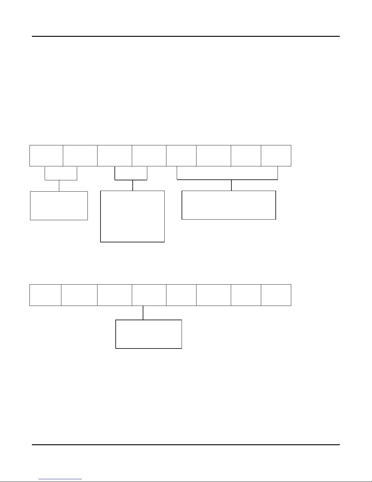
DO2
DO1
Delay
time1
Delay
time0
DI4
DI3
DI2
DI1
X
X
X
Ignition
X X X
X
0 = DI is low *
00= 5 Minutes*
0 = DO is low
0 = Ignition off
5.0 System Resource
5.2 GPIO & Delay Time Setting
5.2.1 GPIO, Delay Time and Ignition Control Register
The General Purpose I/O is an interface available on some devices. These can read
digital signals from other parts of a circuit, or output to control other devices. At GPIO
control register, the GPI is use to receive data, the GPO is set data to send.
I/O port: Read A2h / Write A1h
7 6 5 4 3 2 1 0
1 = DO is high
01= 2 Hours
10= 4 Hours
11= 12 Hours
1 = DI is high
I/O port: D2h
7 6 5 4 3 2 1 0
Status
1 = Ignition on
User’s Manual Page 5-3
Page 65

5.0 System Resource
Read Ignition Register & Example Code
if (pFunc != IntPtr.Zero)
{
UInt32 PortVal;
SetPortValType SetPortVal = (SetPortValType)Marshal.GetDelegateForFunctionPointer(pFunc,
typeof(SetPortValType));
GetPortValType GetPortVal = (GetPortValType)Marshal.GetDelegateForFunctionPointer(pFunc,
typeof(GetPortValType));
SetPortVal(0x4E, 0x87, 1); // Enter Super IO
SetPortVal(0x4E, 0x87, 1); // Enter Super IO
SetPortVal(0x4E, 0x07, 1); // Select Logic 7 for GPIO
SetPortVal(0x4F, 0x06, 1);
SetPortVal(0x4E, 0xD2, 1); // Ignition Status Register bit4
// Call WinIo to get value
bool Result1 = GetPortVal(0x4F, &PortVal, 1); // Read GPIO Status
SetPortVal(0x4E, 0xAA, 1); // exit PNP mode
5.2.2 GPIO Programming Procedure
< // C# use Winio >
(1) Write Register & Example Code
IntPtr pFunc = GetProcAddress(hMod, "SetPortVal");
if (pFunc != IntPtr.Zero)
{
SetPortValType SetPortVal = (SetPortValType)Marshal.GetDelegateForFunctionPointer(pFunc,
typeof(SetPortValType));
SetPortVal(0x4E, 0x87, 1); // Enter Super IO
SetPortVal(0x4E, 0x87, 1); // Enter Super IO
SetPortVal(0x4E, 0x07, 1); // Select Logic 7 for GPIO
SetPortVal(0x4F, 0x06, 1); //
SetPortVal(0x4E, 0xA1, 1); // Set GPIO 5X Address
SetPortVal(0x4F, 0xF0, 1); // Set GPO 0~3 value = "0" means output is low
SetPortVal(0x4E, 0xAA, 1); // exit PNP mode
}
User’s Manual Page 5-4
Page 66
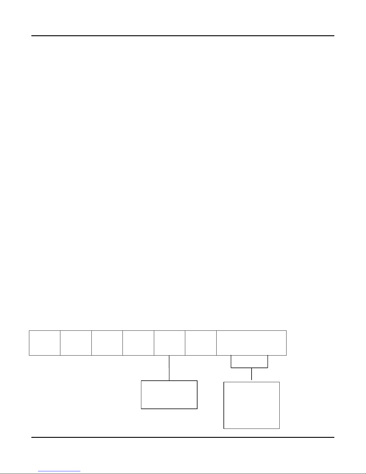
0
0
1
1
Timer
0
Select output pulse
00 = 1 ms
0 = 1 sec
5.0 System Resource
(2) Read Register & Example Code
if (pFunc != IntPtr.Zero)
{
UInt32 PortVal;
SetPortValType SetPortVal = (SetPortValType)Marshal.GetDelegateForFunctionPointer(pFunc,
typeof(SetPortValType));
GetPortValType GetPortVal = (GetPortValType)Marshal.GetDelegateForFunctionPointer(pFunc,
typeof(GetPortValType));
SetPortVal(0x4E, 0x87, 1); // Enter Super IO
SetPortVal(0x4E, 0x87, 1); // Enter Super IO
SetPortVal(0x4E, 0x07, 1); // Select Logic 7 for GPIO
SetPortVal(0x4F, 0x06, 1);
SetPortVal(0x4E, 0xA2, 1); // GPIO Status Register
// Call WinIo to get value
bool Result1 = GetPortVal(0x4F, &PortVal, 1); // Read GPIO Status
5.2.3 WDT Setting
I/O port: 260 (base address) + 05h and 06h
1 Watchdog Timer Control Register
The Watchdog Timer Control Register controls the WDT working mode. Write the value
to the WDT Configuration Port. The following table describes the Control Register bit
definition:
7 6 5 4 3 2 1 0
Unit
width of RSTOUT#
1 = 60 sec *
User’s Manual Page 5-5
01 = 25 ms
10 = 125 ms*
11 = 5 sec
Page 67
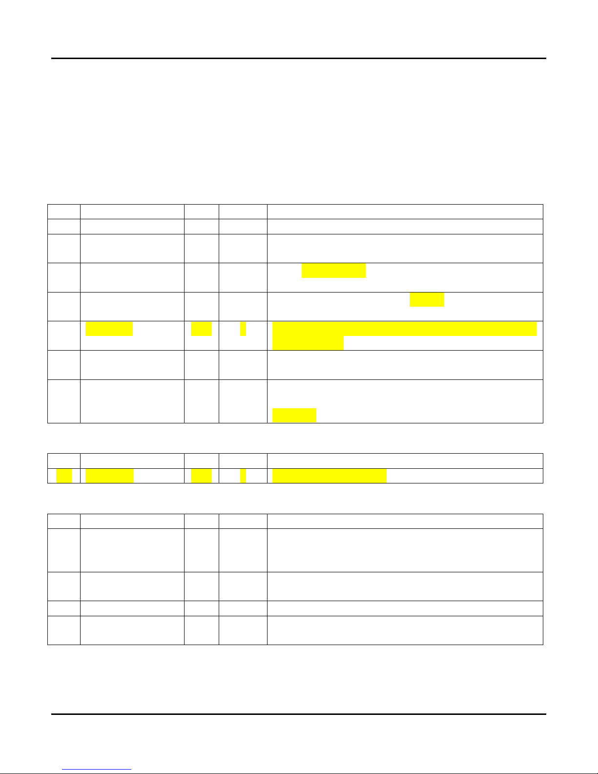
Bit
Name
R/W
Default
Description
7
Reserved
R 0 Reserved
6
WDTMOUT_STS
R/W
0
If watchdog timeout event occurs, this bit will be set to
1. Write a 1 to this bit will clear it to 0.
5
WD_EN
R/W
0
If this bit is set to 1, the counting of watchdog time is
enabled.
4
WD_PULSE
R/W
0
Select output mode (0:level, 1:pulse) of RSTOUT# by
setting this bit.
3
WD_UNIT
R/W
0
Select time unit (0:1sec, 1:60sec) of watchdog timer by
setting this bit.
2
WD_HACTIVE
R/W
0
Select output polarity of RETOUT# (1:high active, 0:low
active) by setting the bit.
1-0
WD_PSWIDTH
R/W
0
Select output pulse width of RSTOUT#
2:125 ms 3:5 sec
Bit
Name
R/W
Default
Description
7-0
WD_TIME
R/W
0
Time of watchdog timer
Bit
Name
R/W
Default
Description
7
WDT_PME
R
--
The PME Status
watchdog timer is 1 unit before time out (of time out)
6
WDT_PME_EN
R/W
0
0 : Disable Watchdog PME.
1 : Enable Watchdog PME
5-1
Reserved
--
--
Reserved
0
WDOUT_EN
R/W
0
0 : disable Watchdog time out output via WDTRST#
1 : enable Watchdog time out output via WDTRST#
5.0 System Resource
Watchdog Timer Function
Watch dog timer is provided for system controlling. If time-out can trigger one signal to
high/low level/pulse, the signal is depend on register setting.
The time unit has two ways from 1sec or 60sec. In pulse mode, there are four pulse
widths can be selected (1ms/25ms/125ms/5sec). Others, please refer the device
register description as below.
Watchdog Timer Configuration Register 1- base address +05h
0:1 ms 1:25 ms
Watchdog Timer Configuration Register 2- base address +06h
Watchdog PME Control Register - base address + 0Ah
This bit will set when WDT_PME_EN is set and the
User’s Manual Page 5-6
Page 68

5.0 System Resource
2 Watchdog Timer Programming Procedure
(1) Example Code
private void button2_Click(object sender, EventArgs e)
{
IntPtr pFunc = GetProcAddress(hMod, "SetPortVal");
if (pFunc != IntPtr.Zero)
{
SetPortValType SetPortVal =
(SetPortValType)Marshal.GetDelegateForFunctionPointer(pFunc, typeof(SetPortValType));
SetPortVal(0x266, 0x0A, 1); // Set watchdog timer value is 10
SetPortVal(0x265, 0x32, 1); // Set watchdog timer unit is sec and enable
watchdog
// SetPortVal(0x265, 0x3A, 1); // Set watchdog timer unit is minuates and enable
watchdog
}
}
User’s Manual Page 5-7
Page 69

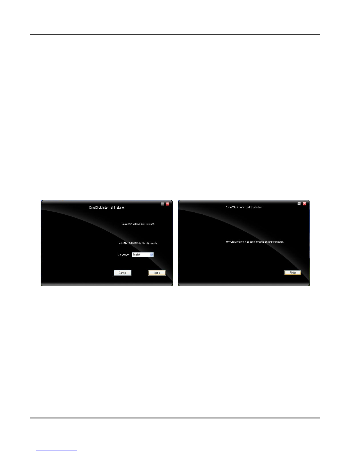
5.3 Gobi2000 WWAN Module Application Note
Document Number: VBOX-3200-WWAN-01
1. EQUIPMENT REQUIREMENTS
2. TEST SETUP
3. TEST
4. PASS/FAIL CRITERIA :
1. EQUIPMENT REQUIREMENTS
• Sierra Wireless Gobi 2000.
• FETnet 3G SIM Card with HSDPA operation.
2. TEST SETUP
5.0 System Resource
Figure 1: Install WWAN AP
Install WWAN AP and configure the EUT with the latest hardware and software. Place
EUT in the test environment, and check the signal of the WWAN module should be as
high as possible. Setup all appropriate test equipment for performing this test.
User’s Manual Page 5-8
Page 70
5.0 System Resource
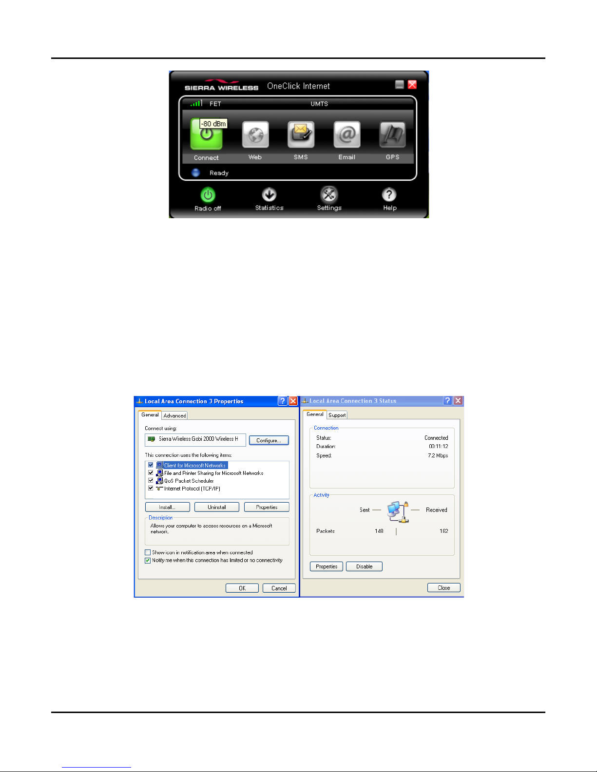
Figure 2: Signal of WWAN Module for UTMS Channels.
3. TEST Procedure
Power-up the EUT until it has completed its boot up process. Place the EUT in building
and check the UMTS/HSDPA signal intensity. Connect to Internet through UMTS/HSDPA
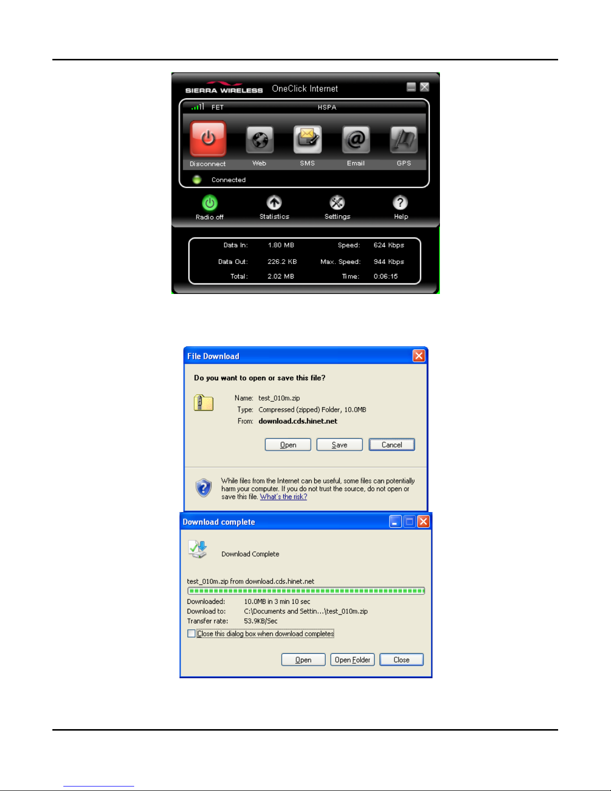
channel. Check the link speed if bandwidth is 7.2Mbps. Download a 10Mbytes test file
from Internet. Record the results from the link states. Make sure it has no any error
while downloading.
Figure 3: Link Speed of WWAN Module for UMTS/HSDPA Channels.
User’s Manual Page 5-9
Page 71
5.0 System Resource
Figure 4: Link State of WWAN Module.
Figure 5: Download Test File from Internet.
User’s Manual Page 5-10
Page 72
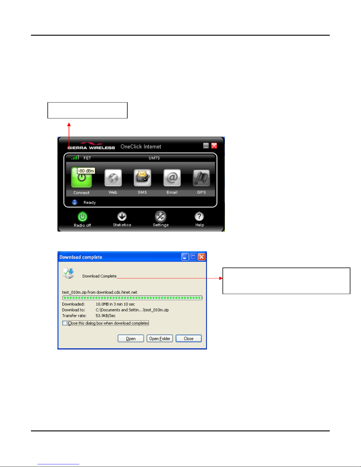
Signal intensity item
Download complete and no any
5.0 System Resource
4. PASS/FAIL CRITERIA :
PASS Criterion : The signal intensity item of the WWAN module must greater than 3
steps. And download test no any error.
error
User’s Manual Page 5-11
Page 73
5.4 Gobi2000 GPS Module Application Note
Document Number: VBOX-3200-GPS-01
1. EQUIPMENT REQUIREMENTS
2. TEST SETUP
3. TEST
4. PASS/FAIL CRITERIA :
1. EQUIPMENT REQUIREMENTS
• Sierra Wireless Gobi 2000.
• FETnet 3G SIM Card with HSDPA operation.
• GPSview program.
2. TEST SETUP
5.0 System Resource
Install WWAN AP and configure the EUT with the latest hardware and software. Place
EUT in the test environment, and check the signal of the WWAN module should be as
high as possible. Setup all appropriate test equipment for performing this test.
User’s Manual Page 5-12
Figure 1: Install WWAN AP
Page 74
5.0 System Resource
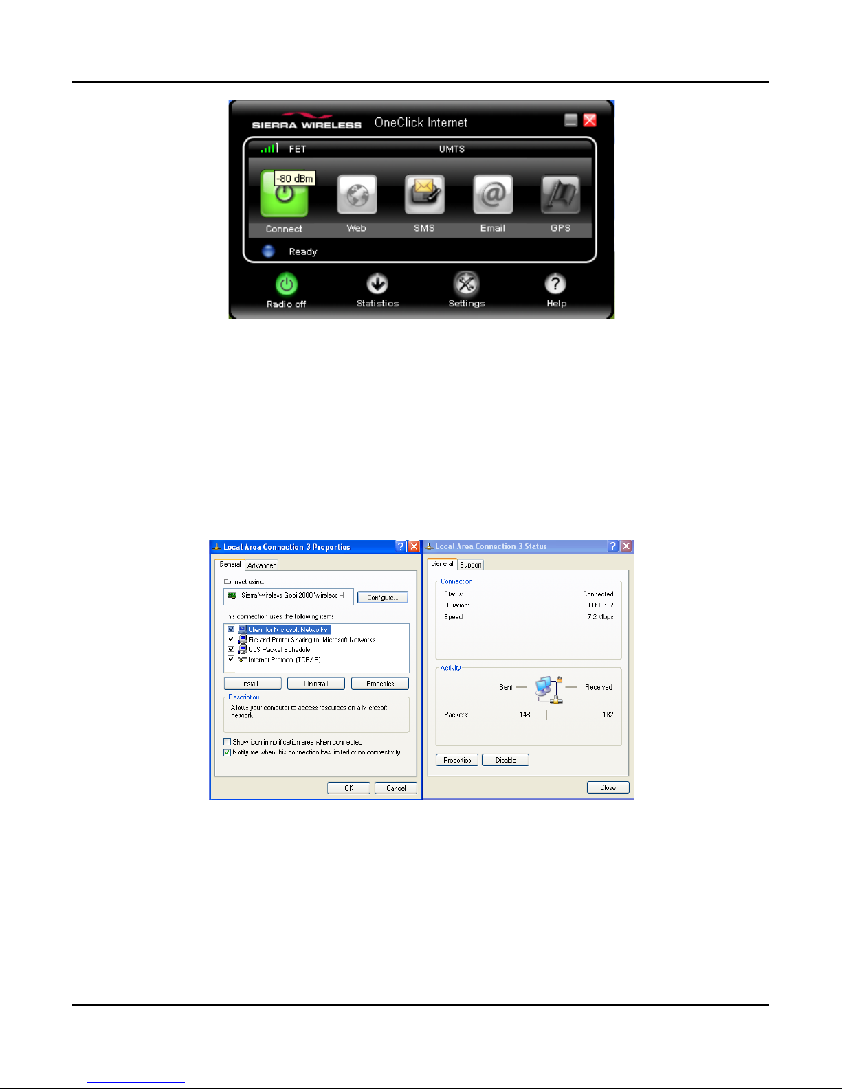
Figure 2: Signal of WWAN Module for UTMS Channels.
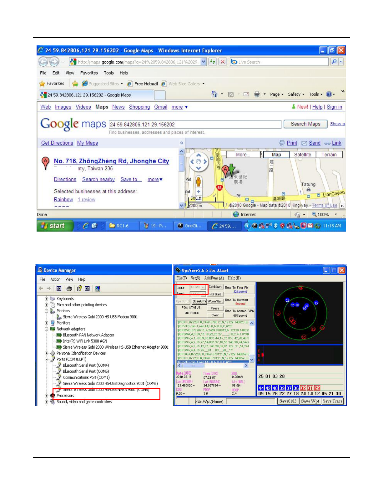
3. TEST
Out door power-up the EUT until it has completed its boot up process. Place the EUT
in building and check the UMTS/HSDPA and GPS signal intensity. Get GPS longitude and
latitude; connect to Internet through UMTS/HSDPA channel. Check Google Maps and
GPSview satellite set and fix time.
Figure 3: Link Speed of WWAN Module for UMTS/HSDPA Channels.
User’s Manual Page 5-13
Page 75
5.0 System Resource
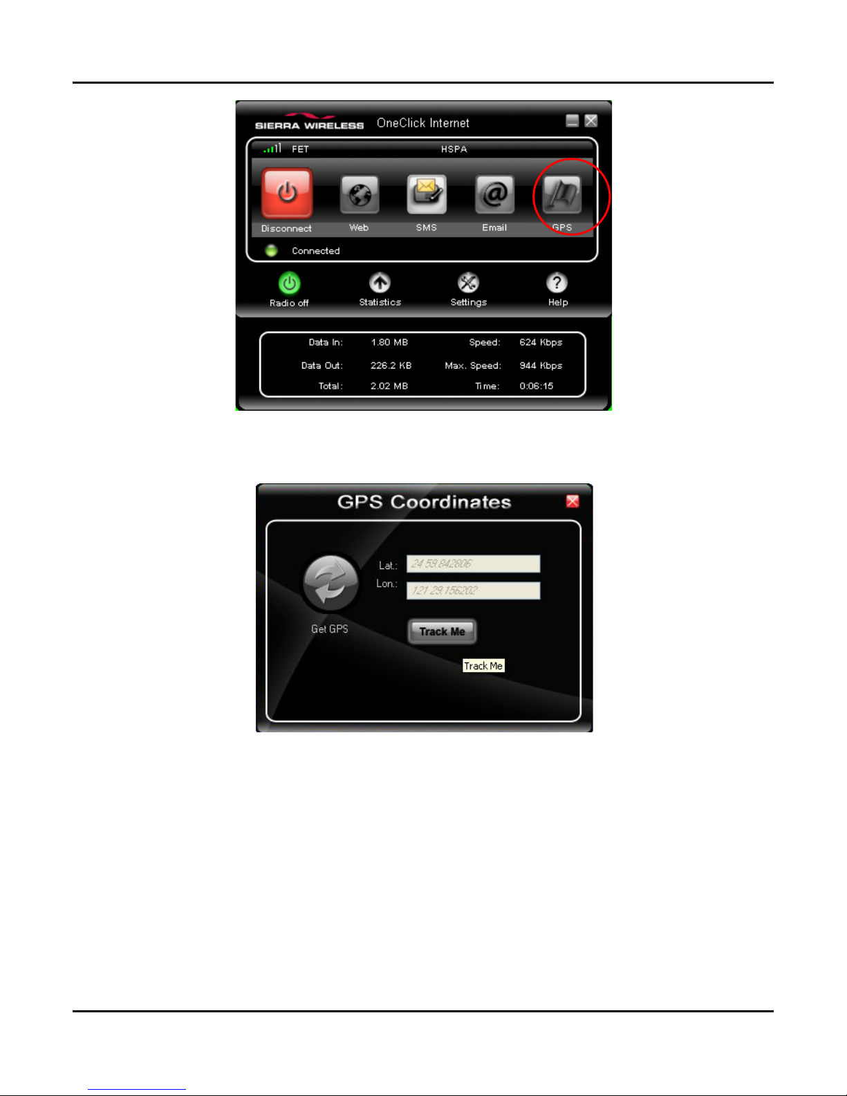
Figure 4: Link State of WWAN Module.
Figure 5: GPS longitude and latitude information.
User’s Manual Page 5-14
Page 76
5.0 System Resource
Figure 6: Link to Google Maps.
User’s Manual Page 5-15
Figure 7: GPSview program test.
Page 77
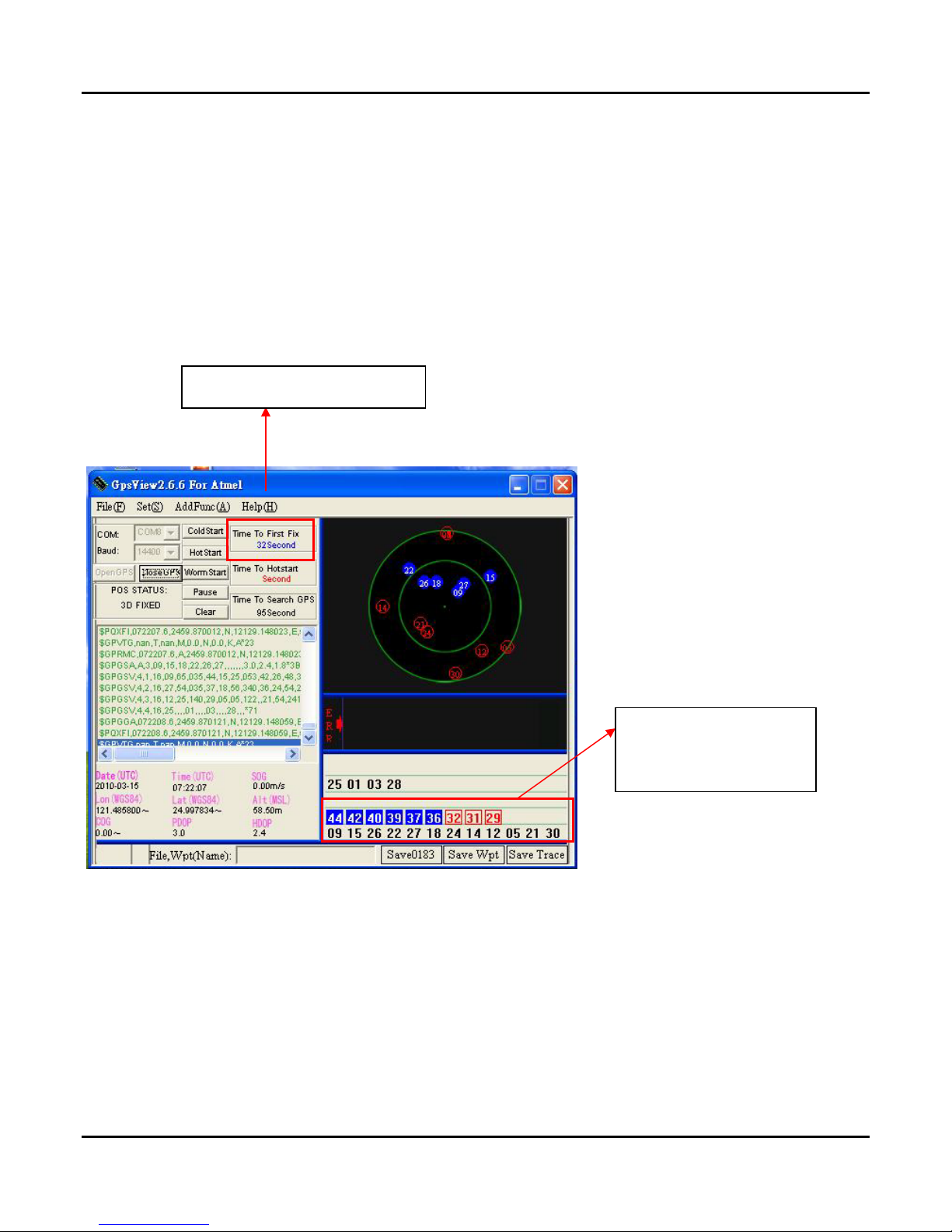
satellite set and fix time
amount of satell it e
5.0 System Resource
4. PASS/FAIL CRITERIA :
PASS Criterion :
We must check two results. One is amount of satellite, and another one is the satellite
set and fix time.
The amount of satellite must exceed five satellites, and the intensity must exceed 30.
The satellite set and fix time must be smaller than 60 sec.
User’s Manual Page 5-16
and intensi ty
Page 78

6.0 BIOS
6.0
BIOS
User’s Manual
Page 79
6.0 BIOS
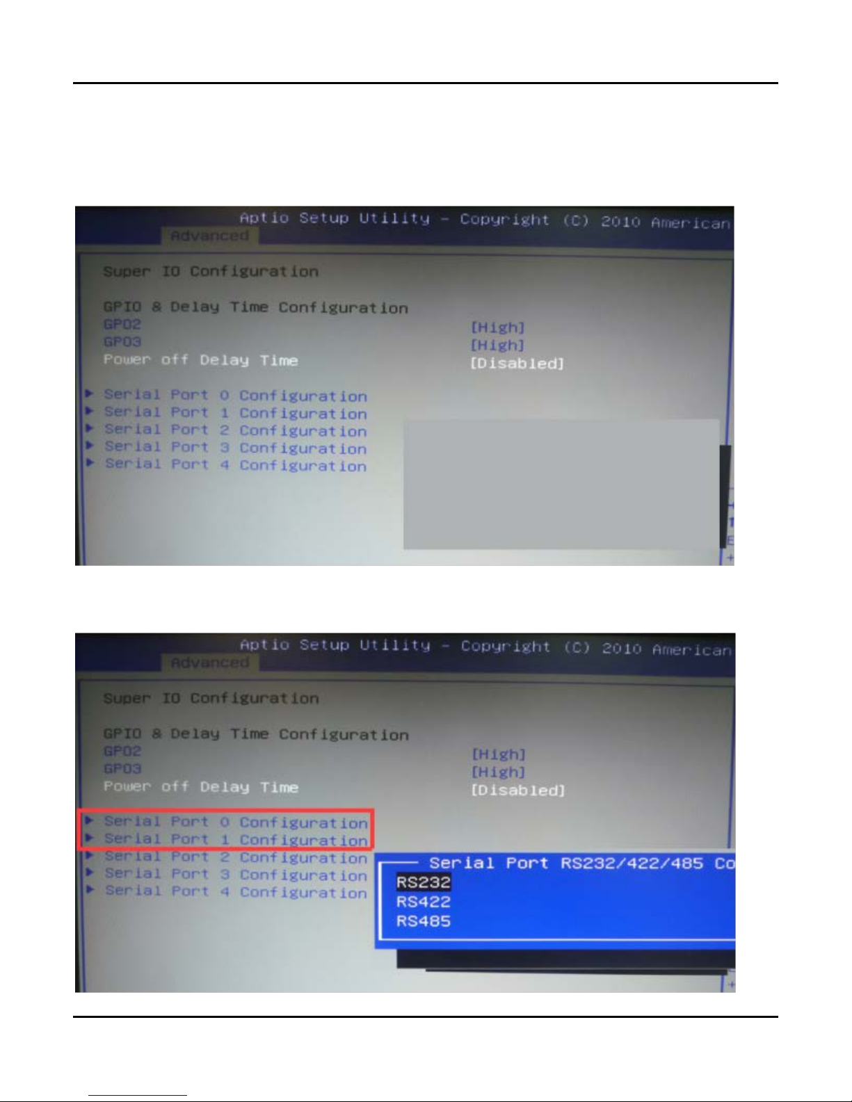
6.1 Super IO Configuration
6.0 BIOS
Select Serial Port Mode
User’s Manual Page 6-1
Page 80
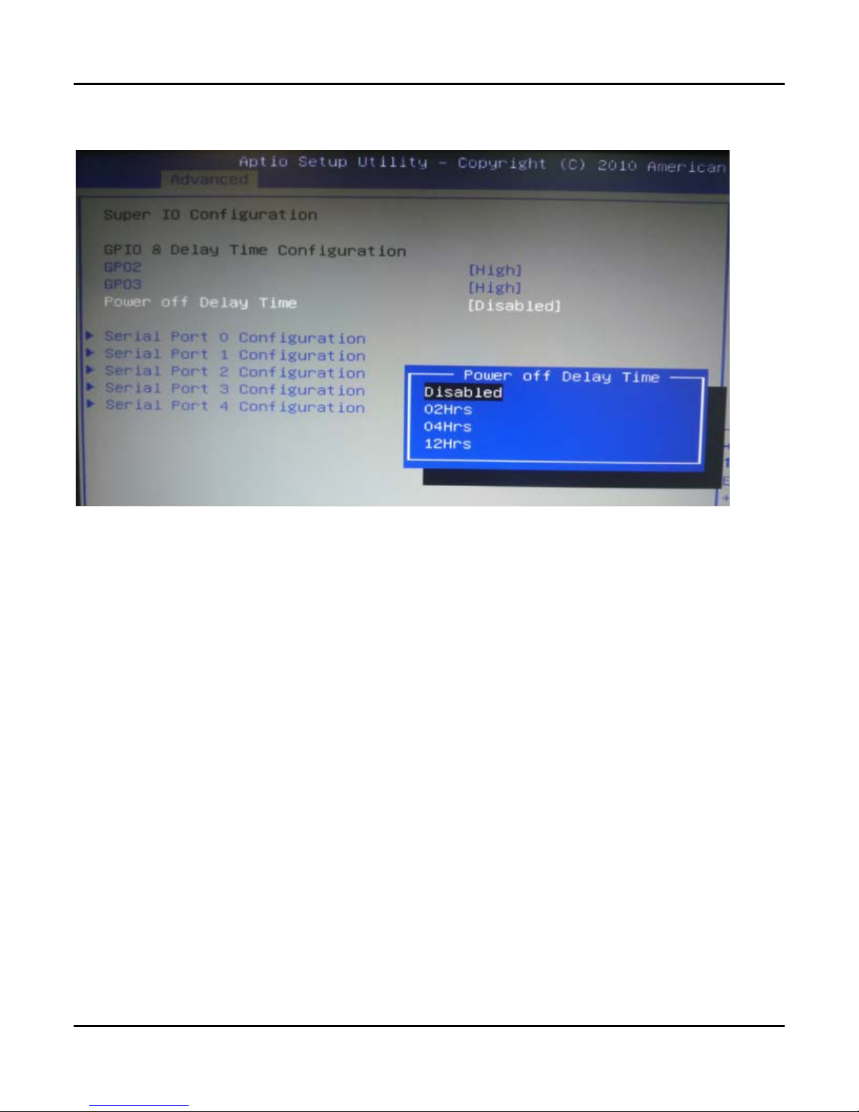
Select Power off Delay Time
6.0 BIOS
User’s Manual Page 6-2
Page 81

7.0 Packing List
7.0
PACKING LIST
User’s Manual
Page 82
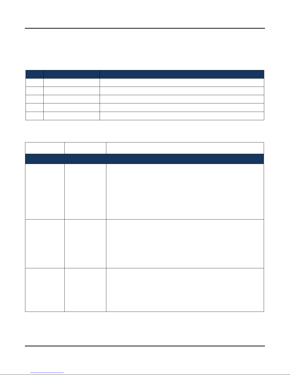
Item
Part Number
Module Name
1
663200001000
VBOX-3200-T56N/2GB
2
370832001100
VBOX-3200 Mount Bracket
3
351103040250
Screw F Type M3*4L ISO BK
4
326710039661
CABLING PHOENIX CON MALE 3PIN
5
324610088661
CABLING PHOENIX CON MALE 8PIN
LTE – DD 800MHz (Band 20) / 900MHz (Band 8) /2600MHz (Band 7)
(3G or 4G Antenna Kit be included)
HSDPA/UMTS –800/850/900/1900/2100MHz
(3G Antenna Kit be included)
Single
7.0 PACKING LIST
7.1 Packing List
Optional
Part No. Vendor / Model Description
7.0 Packing List
577710140090
573000011092
573000120009
MC7710
Gobi3000-Dual
(MC8355)
Gobi3000-
(MC8305)
/ 1800MHz (Band 3 ) / 2100MHz (Band 11) MHz
DC-HSPA+1/HSPA+/HSUPA/HSDPA/UMTS – 900/2100MHz
Quad-band EDGE/GPRS/GSM – 850/900/1800/1900MHz
GPS is Standalone, gpsOne XTRA assistance for enhanced
standalone GPS performance, MS-based assisted
(support varies based on network carrier)
Quad-band EDGE/GPRS/GSM –850/900/1800/1900MHz
Dual-band EV-DO/CDMA –800/1900MHz
GPS is Standalone, gpsOne XTRA assistance for enhanced
standalone GPS performance, MS-based assisted
(support varies based on network carrier)
HSDPA/UMTS –850/900/1800/1900/2100MHz
Quad-band EDGE/GPRS/GSM –850/900/1800/1900MHz
Single-band CDMA –1900MHz
GPS is Standalone, gpsOne XTRA assistance for enhanced
standalone GPS performance, MS-based assisted
(3G Antenna Kit be included)
User’s Manual Page 7-1
Page 83

HSDPA/UMTS –850/900/1900/2100MHz
(3G Antenna Kit be included)
578090120091
570800100109
(MC8090)
VDB-800S
570800100101 VDB-800DR
7.0 Packing List
Quad-band EDGE/GPRS/GSM –850/900/1800/1900MHz
Single-band CDMA –1900MHz
GPS is Standalone, gpsOne XTRA assistance for enhanced
standalone GPS performance, MS-based assisted
Supports Voice function
Embedded u-blox6 GPS Mini PCIe Card
Very high sensitivity (Tracking Sensitivity: -160 dBm)
50 Channels / Hot Start 1s / Warm Start 28s / Cold Start 28s
AssistNow Online and Offline A-GPS Services,OMA SUPL Compliant
Support NMEA 0183 V3.0
Update Rate 5 Hz (Max.)
(GPS Active Antenna be included)
Embedded u-blox6 GPS with Dead Reckoning and G-sensor Mini
PCIe Card
Very high sensitivity (Tracking Sensitivity: -160 dBm)
50 Channels / Hot Start 1s / Warm Start 40s / Cold Start 45s
Support NMEA 0183 V3.0
AssistNow Online and Offline A-GPS Services, OMA SUPL Compliant
100% Coverage with Continuous Position Fixes Even in Tunnels
Highly Accurate and Reliable Navigation Performance
Automatic Sensor Calibration and Temperature
Include odometer cable.
(GPS Active Antenna be included)
570800160009 VDB-800SG
346123002001
VDB-801
User’s Manual Page 7-2
Embedded u-blox6 GPS Mini PCIe Card and G-sensor
Very high sensitivity (Tracking Sensitivity: -160 dBm)
50 Channels / Hot Start 1s / Warm Start 28s / Cold Start 28s
AssistNow Online and Offline A-GPS Services,OMA SUPL Compliant
Support NMEA 0183 V3.0
Update Rate 5 Hz (Max.)
(GPS Active Antenna be included)
50-channel u-blox6 Engine with Over 2 Million Effective Correlators
146dBm SuperSense® Acquisition and Tracking Sensitivity
AssistNow Online and Offline A-GPS Services,OMA SUPL Compliant
100% Coverage with Continuous Position Fixes Even in Tunnels
Highly Accurate and Reliable Navigation Performance
Automatic Sensor Calibration and Temperature
Operating Temperature : -40ºC to 80ºC
Page 84
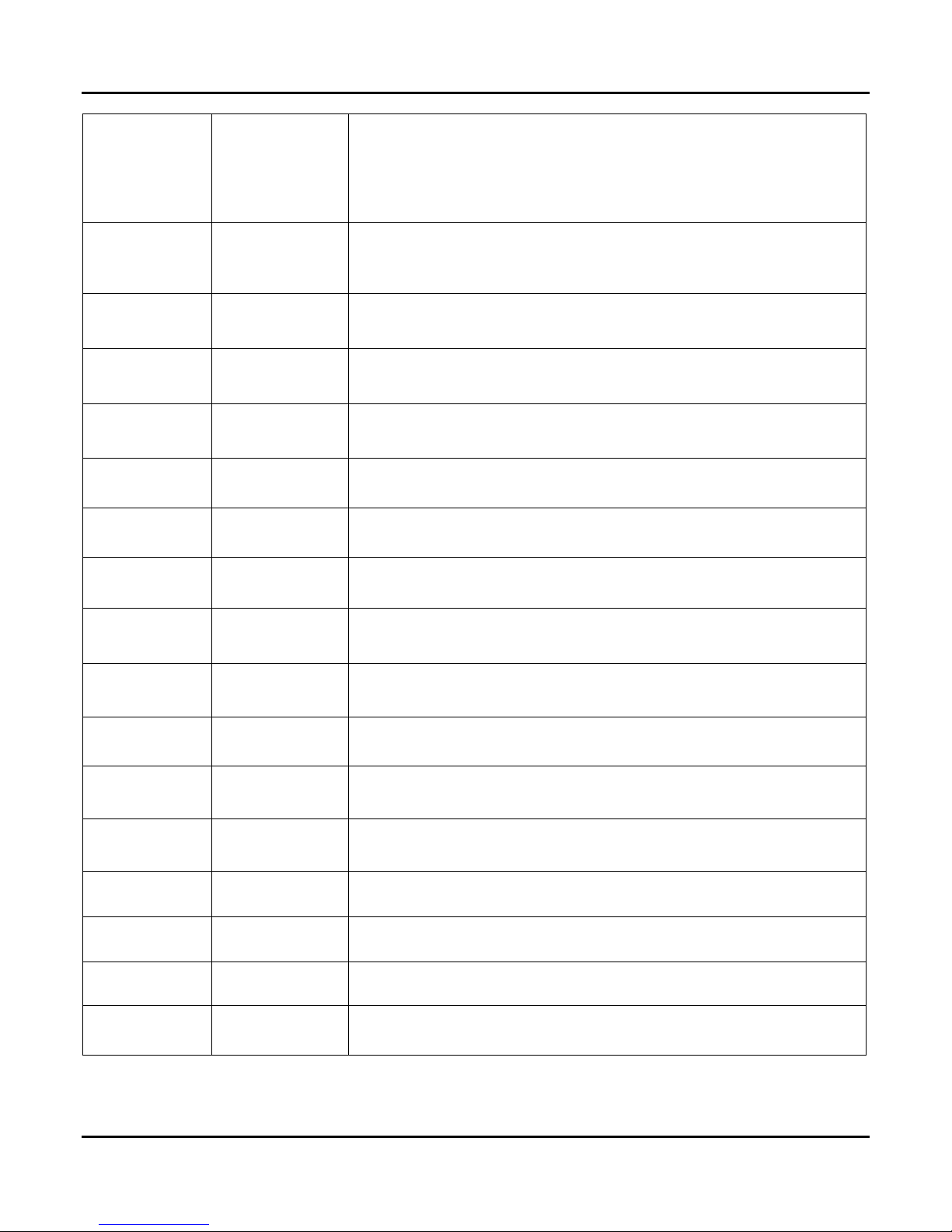
mini card,
570802090009 Q802XKN3B
7.0 Packing List
Ralink(RT3090BC4) 1X1 802.11n, Wireless Lan and CSR Bluecore4
Bluetooth2.1+EDR (Microsoft in-box driver, profiles;Motorola
profiles) / software upgradable to BT3.0+HS(Motorola) Combo
Mini-PCIe Card (Wifi Antenna Kit be included)
570195090090
DHXA-195
570802010009 Q802XKN5F
570802011009 Q802XKN5
571350010090
DNXA-116
802.11n b/g 1x1 wifi plus Bluetooth combo PCIe half-size
WB195/AR9285+AR3011 (Wifi Antenna Kit be included)
Ralink 802.11b/g/N, 2T2R,Mini PCIe Card (Full size)
(Wifi Antenna Kit be included)
Ralink 802.11b/g/N, 2T2R,Mini PCIe Card (Half size)
(Wifi Antenna Kit be included)
802.11 a/b/g/n, Atheros AR9382, 2T2R, Half-size Mini-PCIe card
(Wifi Antenna Kit be included)
345570033000 7-in-1-1dBi-5M GPS+3G+WIFI Combo Antenna SMA Male, 7-in-1 Multi-band / 5M
342631091000
WiFi-2dB Wifi Antenna 2dBi / 2.4G / SMA Female ( silver color)
342631391031 WiFi-5dB-3M Wifi Antenna 5dBi / 2.4G / 3M / SMA Male (Flat Type)
343131091000
3G-2dBi 3G Antenna 2dBi / 3.5G / GPRS / SMA Female (gold color)
344220033000 3G-1.5dBi-3M 3G Antenna 1.5dBi / 3.5G / GPRS / 3M / SMA Female (Flat Type)
343225003000 GPS-Passive-5M GPS Passive Antenna 5M / SMA male (Only for GOBI Series)
343235002000 GPS-Active-5M GPS Active Antenna 5M / SMA male
221401280005 BAT-3000 Neosonic-Polymer 800mAH 3S1P Battery kit for VBOX-3200
972009720000
970000750000
970007740000
970022730000
User’s Manual Page 7-3
Microsoft Windows Embedded Standard 2009 (Windows XP Embedded)
Microsoft Windows XP Pro license fee
Microsoft Windows® Embedded Standard 7 Runtime (WS7E)(ESD)
Microsoft Windows® 7 Professional for Embedded Systems x32/x64
Page 85
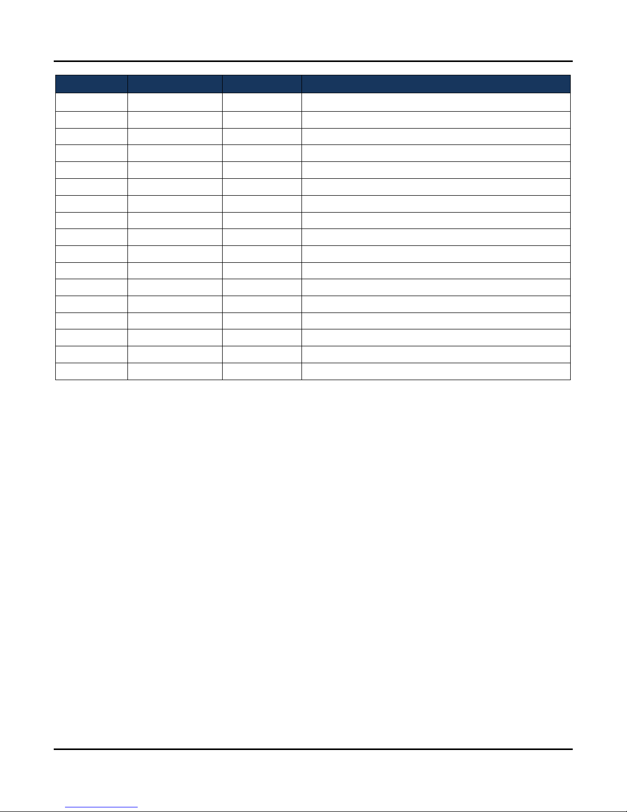
7.0 Packing List
User’s Manual Page 7-4
 Loading...