

Page 1

VBOX-3000
In-Vehicle Computing
User's Manual
Version 1.1
Page 2

SINTRONES® Technology Corp.
User Manual
Copyright
©2009 by SINTRONES® Technology Corp. All Rights Reserved.
No part of this publication may be reproduced, transcribed, stored in a retrieval system, translated into any language, or transmitted in any form or by any means such as
electronic, mechanical, magnetic, optical, chemical, photocopy, manual, or otherwise,
without prior written permission from SINTRONES® Technology Corp.
Other brands and product names used herein are for identication purposes only and
may be trademarks of their respective owners.
Disclaimer
SINTRONES® Technology Corp. shall not be liable for any incidental or consequential
damages resulting from the performance or use of this product.
SINTRONES® Technology Corp. makes no representation or warranty regarding the
content of this manual. Information in this manual had been carefully checked for
accuracy;however, no guarantee is given as to the correctness of the contents. For
continuing product improvement, SINTRONES® Technology Corp. reserves the right
to revise the manual or make changes to the specications of this product at any time
without notice and obligation to any person or entity regarding such change. The information contained in this manual is provided for general use by customers.
This device complies to Part 15 of the FCC Rules. Operation is subject to the following two conditions:
1. This device may not cause harmful interference.
2. This device must withstand any background interference including those that may
cause undesired operation.
Page 3

Safety Information
Read the following precautions before setting up a SINTRONES Product.
Electrical safety
•
To prevent electrical shock hazard, disconnect the power cable from the electrical
outlet before relocating the system.
•
When adding or removing devices to or from the system, ensure that the power
cables for the devices are unplugged before the signal cables are connected.
If possible, disconnect all power cables from the existing system before you add a
device.
•
Before connecting or removing signal cables from the motherboard, ensure that all
power cables are unplugged.
•
Seek professional assistance before using an adapter or extension cord.
These devices could interrupt the grounding circuit.
•
Make sure that your power supply is set to the correct voltage in your area.
If you are not sure about the voltage of the electrical outlet you are using, contact
your local power company.
•
If the power supply is broken, do not try to x it by yourself. Contact a qualied
service technician or your retailer.
Operation safety
•
Before installing the motherboard and adding devices on it, carefully read all the
manuals that came with the package.
•
Before using the product, make sure all cables are correctly connected and the
power cables are not damaged. If you detect any damage, contact your dealer
immediately.
•
To avoid short circuits, keep paper clips, screws, and staples away from connectors,
slots, sockets and circuitry.
•
Avoid dust, humidity, and temperature extremes. Do not place the product in any
area where it may become wet.
•
Place the product on a stable surface.
•
If you encounter technical problems with the product, contact a qualied service
technician or your retailer.
CAUTION
Incorrectly replacing the battery may damage this computer. Replace only with
the same or its equivalent as recommended by SINTRONES® Technology
Corp. Dispose used battery according to the manufacturer's instructions.
Page 4

TABLE OF CONTENTS
1 Function Introduction
1.1 Model Specications.......................................................................................6
1.2 VBOX-3000 Illustration <Mainboard, System> ..............................................7
1.3 Memory Module Installation ...........................................................................9
1.4 Power Supply ...............................................................................................10
1.5 Ignition Power Management Quick Guide ....................................................11
1.6 RJ-45 LAN Connector LEDs ........................................................................13
1.7 Connectors Guide ........................................................................................15
1.8 Jumpers Guide .............................................................................................22
2 System Installation
2.1 System Introduction .....................................................................................24
2.2 Opening Chassis with Battery Kit .................................................................25
2.3 Opening Chassis without Battery Kit ............................................................26
2.4 Installing HDD with Battery Kit .....................................................................27
2.5 Installing HDD without Battery Kit ................................................................28
2.6 Installing Memory .........................................................................................29
2.7 Installing SDD ..............................................................................................30
2.8 Installing 3G Module ....................................................................................31
2.9 Installing SIM Card .......................................................................................32
2.10 Installing MINI PCI Express Expansion Card (WiFi Module) .......................33
2.11 Installing Battery Module ..............................................................................34
3 BIOS
3.1 Entering The BIOS .......................................................................................35
3.2 Main ..............................................................................................................37
3.3 Advanced .....................................................................................................38
3.4 Boot ..............................................................................................................43
3.5 Security ........................................................................................................44
3.6 Chipset .........................................................................................................45
3.7 Power ...........................................................................................................46
3.8 Exit ...............................................................................................................48
Page 5

4 System Resources
4.1 Watch Dog Timer Setting .............................................................................49
4.2 GPIO Settting ...............................................................................................50
4.3 AMI Post Code .............................................................................................51
4.4 Resource List ...............................................................................................55
5 Packing List
5.1 Packing List ..................................................................................................57
English
5
Page 6

English
1 Function Introduction
1.1 Model Specifications
CPU • Intel Atom N270 1.6GHz Processor with 533MHz FSB
Chipset • Intel 945GSE + ICH7M
Memory • 1 x DDRII-533 SO-DIMM Up to 2GB
Display • Integrated Intel GMA-950 GFx Core in 945GSE MCH
ATA • 1 x Serial ATA port with 150MB/s HDD transfer rate
LAN Chipset • 2 x Intel 82574L Gigabit Ethernet
Watchdog • 1 ~ 255 level reset
Serial Port • Support 2 x RS-232 with 5V/12V Output (COM1 with RS-232422485)
USB Port • 3 x USB 2.0 ports
LAN • 2 x RJ45 ports for GbE
Video Port • 1 x DVI-I Female Connector for DVI-D and VGA Output
GPIO Port • Support 2 in and 2 out with Relay 12V / 100mA
Audio • Mic-in/Line-out
Expansion Bus • 2 x Mini-card slot
Antenna • 4 x SMA-type External Antenna Connectors for WLAN / UMTS / GSM /
GPRS / GPS / Bluetooth
Storage • 1 x 2.5" drive bay for SATA Type Hard Disk Drive / SSD
Qualication • CE, FCC
Power Input • 9V - 36V DC Power Input with 1500VDC Isolation
Power Protection • Automatics Recovery Short Circuit Protection
Power Management • Vehicle Power Ignition for Variety Vehicle
Power Off Control • Power off Delay Time Setting by Software, Default is 5 Mins
Backup Battery • Internal Battery Kit for 10 Mins Operating (Optional)
6
Page 7
Operating Temp. • -20 ~ -70°C (SSD), ambient w/ air
Storage Temp. • -40 ~ 80°C
Relative Humidity• 10 ~ 90% (non-condensing)
Vibration • MIL-STD-810F, Method 514.5, Category 20, Ground Vehicle-Highway
Truck Storage • MIL-STD-810F, Method 514.5, Category 24, Integrity Test
Shock & Crash • Operating : MIL-STD-810F, Method 516.5, Procedure I, Trucks and
semi-trailers=40G (11ms), Non-Operating 80G with SSD
Crash Hazard • MIL-STD-810F, Method 516.5, Procedure V, Ground Equipment=100g
Construction • Aluminum alloy
Mounting • Supports both of wall-mount/VESA-mount
Weight • 1406g
Dimensions • 182 x 167.6 x 35mm
English
• 182 x 167.6 x 47mm (with battery kit)
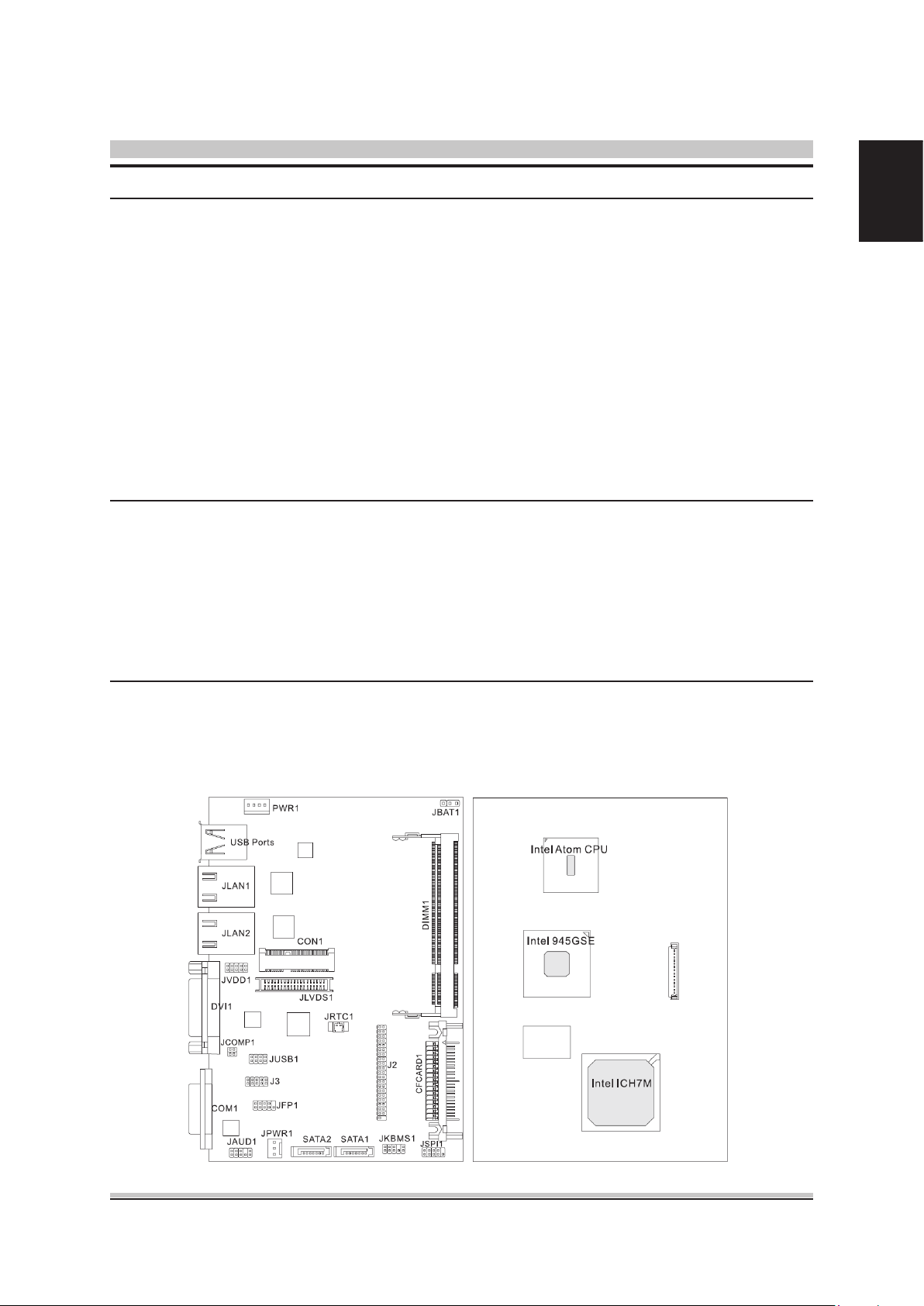
1.2 VBOX-3000 Illustration
Mainboard
7
Page 8
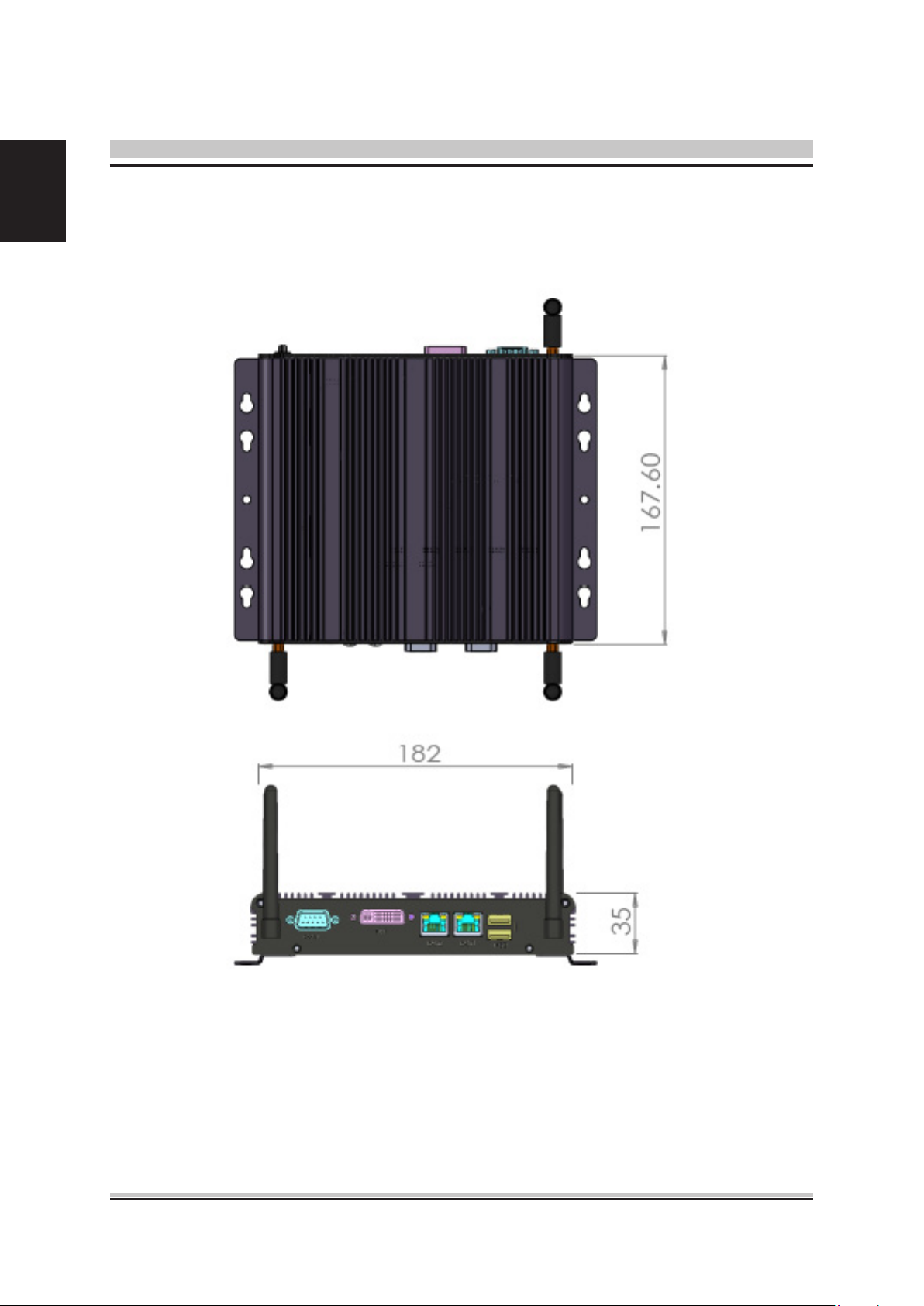
English
System
8
Page 9
1.3 Memory Module Installation
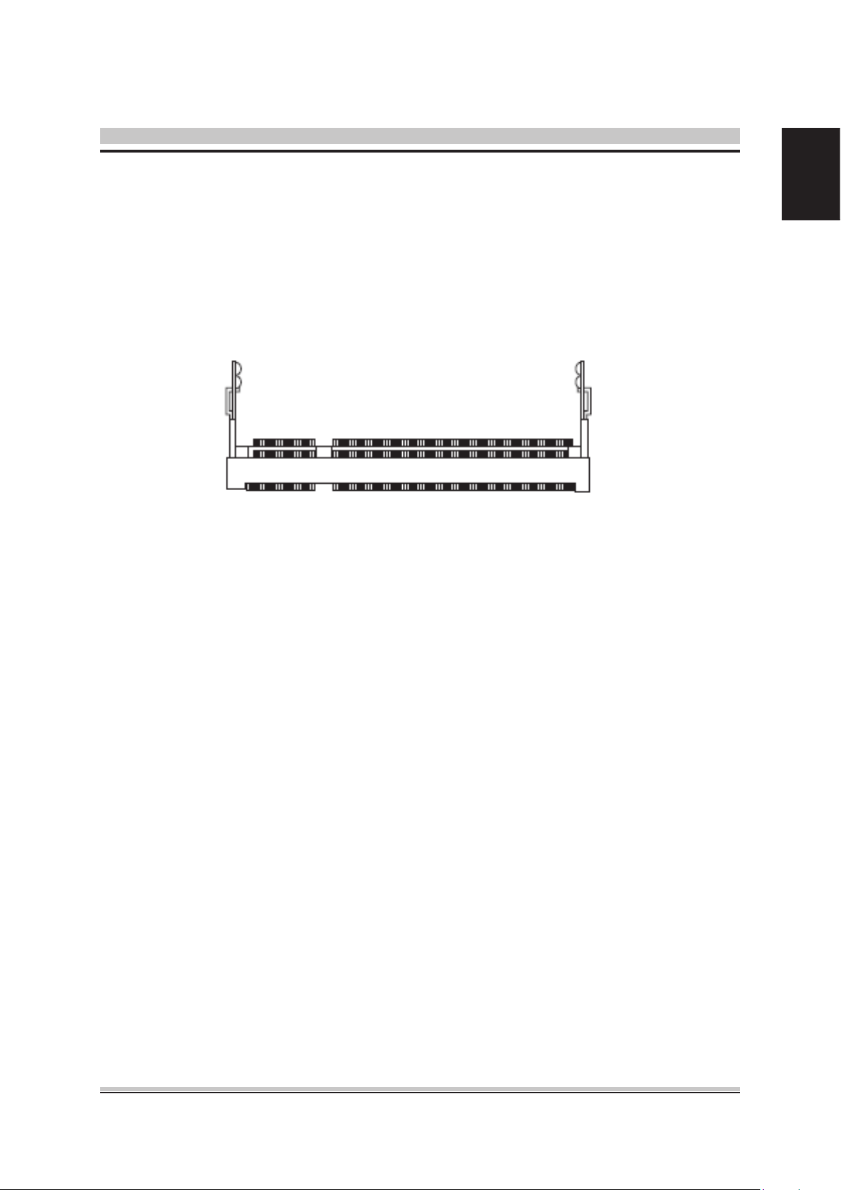
The VBOX-3000 provide one 200pins SODIMM slot for DDR2 533MHz SDRAM memory modules and supports memory sizes up to 2GB.
These DIMM slots are inteded for memory modules.
DDR2 SO-DIMM Slot
200-pin, 1.8V
English
Installing Memory Module
1. Locate the DIMM1 SO-DIMM slot. Align the notch on the DIMM with the key on the
slot and insert the DIMM into the slot at 45-degree angle.
2. Push the DIMM gently forwards until the slot levers click and lock the DIMM in place.
Follow the same procedures to install the second DIMM if necessary.
3. To uninstall the DIMM, ip the slot levers outwards and the DIMM will be released
instantly.
Important
You can barely see the golden nger if the DIMM is properly inserted in the DIMM slot.
9
Page 10
English
1.4 Power Supply
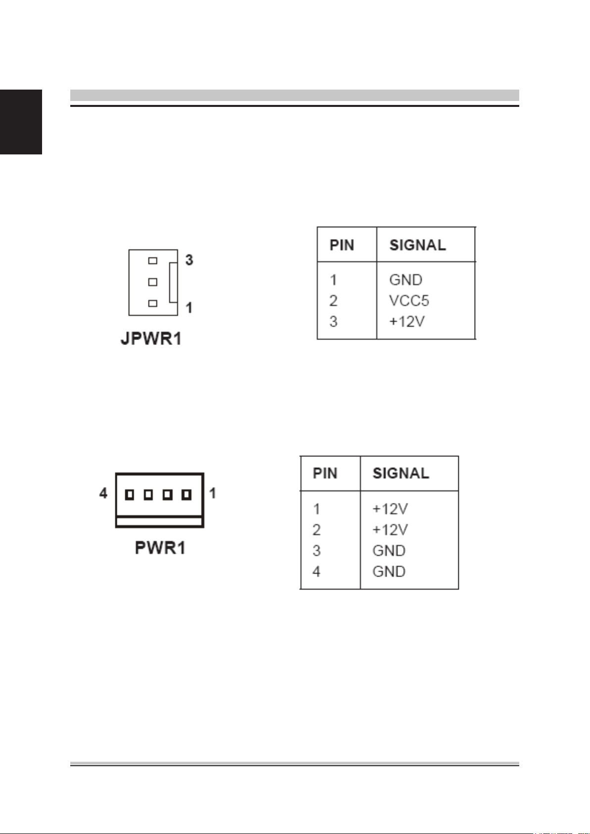
5V/12V HDD Power Connector : JPWR1
This connector provides power to the hard disk drives.
12V System Power Connector : PWR1
This connector provides power to the hard disk drives.
Important
Power supply of 200watts (and above) is highly recommended for system stability.
10
Page 11
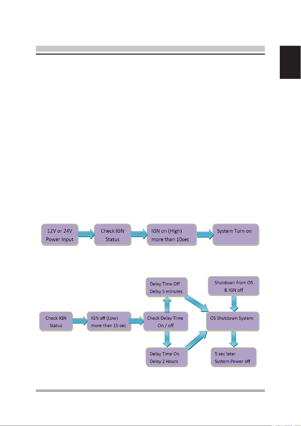
1.5 Ignition Power Management Quick Guide
Startup/shutdown conditions from the IGNITION signal :
1. IGNITION startup signal must be valid during 10 sec. (anti noise protection).
2. IGNITION shutdown – IGNITION signal must be inactive during 5 minutes, then PIC
controller initiate Power Button signal (OS must be set to shutdown from the Power
Button). It generate Main Button shutdown event and then goes to complete power
off.
Typically the system can start only from IGNITION signal, because startup PIC controller
is disconnected from the power source.
The system can be switched off from:
1. Power IGNITION OFF signal.
2. ACPI OS shutdown
3. Power Button - generate ACPI event (OS Dependent)
English
Power Ignition Startup Procedure
Power Ignition Shutdown Procedure
11
Page 12

English
Power Management
1. Power-off delay time is selectable by BIOS to disable and enable in 5 min / 2Hrs.
2. Ignition On/Off status detectable by SW
3. If the ignition is off and the system is still on after 5 minutes, VBOX-3000 will shut
down automatically.
4. If the ignition is turned on again and the power-off delay is in progress, VBOX-3000
will cancel the delay function and will continue to operate normally.
5. If the ignition is turned on again and the power-off delay ended, VBOX-3000 will shut
down completely will power-on again automatically.
12
Page 13
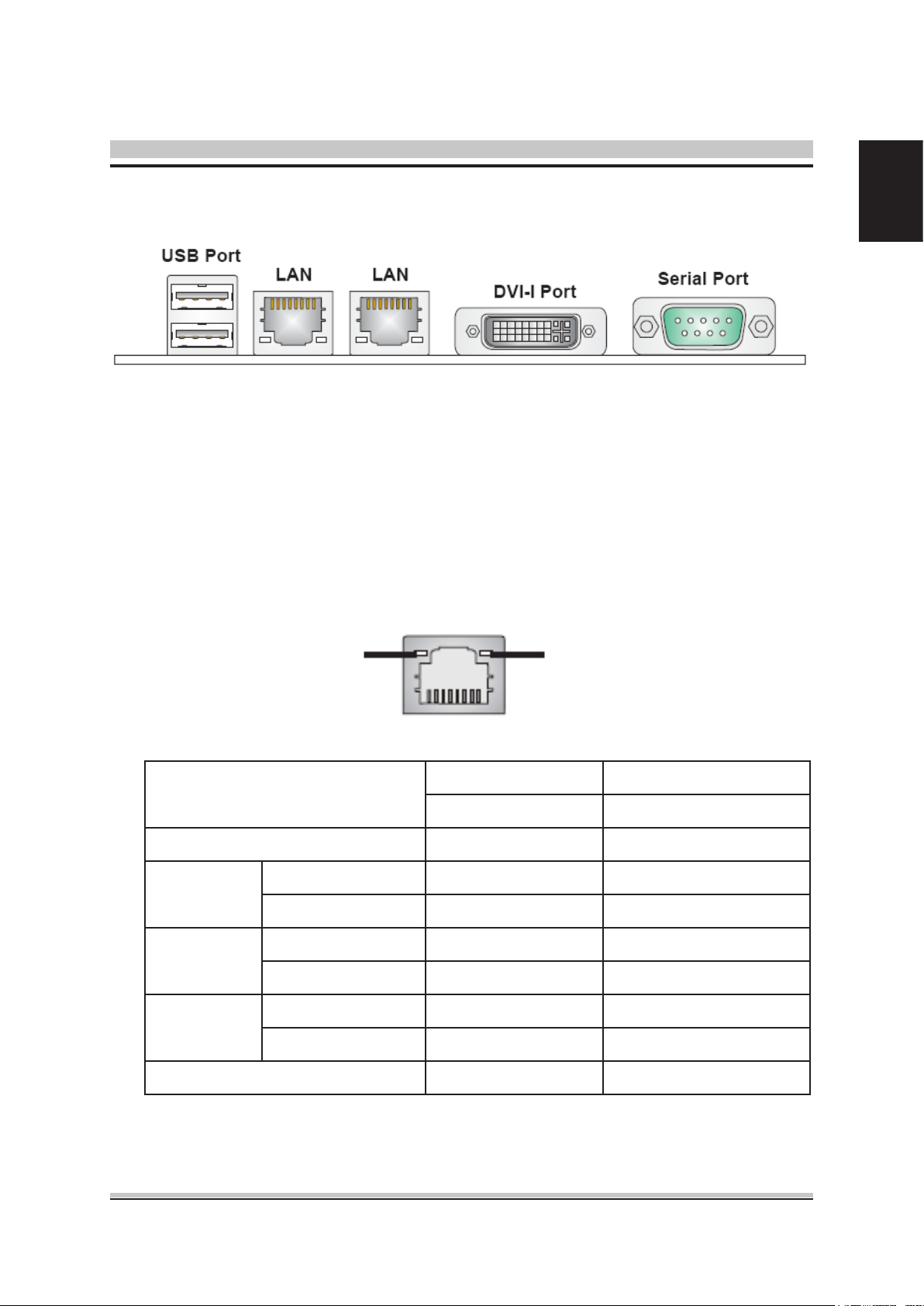
1.6 RJ-45 LAN Connector LEDs
USB Port
The USB (Universal Serial Bus) port is for attaching USB devices such as keyboard,
mouse, or other USB-compatible devices.
LAN
The standard RJ-45 LAN jack is for connection to the local Area Network (LAN). You
can connect a network cable to it.
Speed IndicatorActivity Indicator
English
Left LED Right LED
Active LED 100M/1000 Speed LED
LED Color Yellow Green/Orange
10M Cable
Plug-in
100M Cable
Plug-in
1000M Cable
Plug-in
In S3/S4/S5 standby State Green (Lighting) OFF
No Transmission OFF OFF
Transition Yellow (Blinking) OFF
No Transmission OFF Green (Lighting)
Transition Yellow (Blinking) Green (Lighting)
No Transmission OFF Orange (Lighting)
Transition Yellow (Blinking) Orange (Lighting)
13
Page 14
English
DVI-I Port
The DVI-I (Digital Visual Interface-Integrated) connector allows you to connect an LCD
monitor. It provides a high-speed digital interconnection between the computerand its
display device. To connect an LCD monitor, simply plug your monitor cable into the DVI
connector, and make sure that the other end of the cable is properly connected to your
monitor (refer to your monitor manual for more information.)
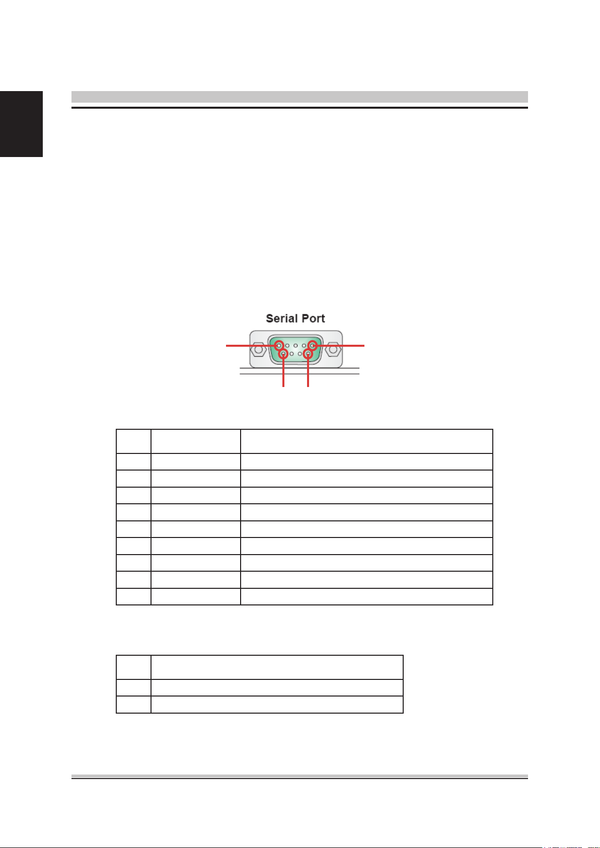
Serial Port
The serial port is a 16550A high speed communications port that sends/ receives 16
bytes FIFOs. You can attach a serial mouse or other serial devices directly to the connector.
1 5
6 9
RS232 Function
PIN SIGNAL DESCRIPTION
1
2
3
4
5
6
7
8
9
RS485 Function
DCD
RXD
TXD
DTR
GND
DSR
RTS
CTS
VCC_COM1
Data Carrier Detect
Receive Data
Transmit Data
Data Terminal Ready
Signal Ground
Data Set Ready
Request To Send
Clear To Send
Voltage output, voltage select setting by J1
PIN DESCRIPTION
14
1 485-, RS-485 transmission line, negative
3 485+, RS-485 transmission line, positive
Page 15
RS422 Function
PIN DESCRIPTION
1 422TXD-, RS-422 transmission line, negative
2 422RXD+, RS-422 receiving line line, positive
3 422TXD+, RS-422 transmission line, positive
4 422RXD-, RS-422 receiving line, negative
1.7 Connectors
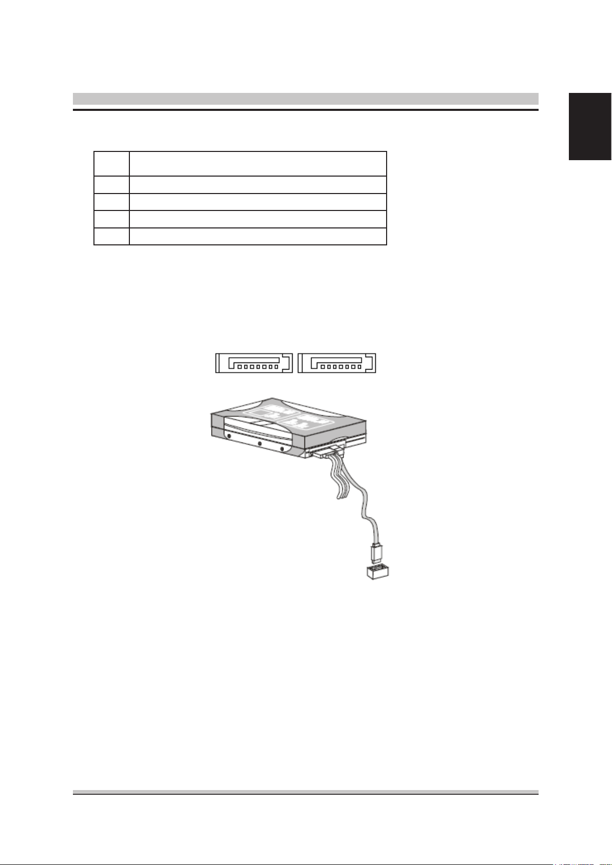
Serial ATA II Connector : SATA1, SATA2
This connector is a high-speed Serial ATA II interface port. Each connector can connect
to one Serial ATA II device.
English
Important
Please do not fold the Serial ATA cable into 90-degree angle. Otherwise, data loss may
occur during transmission.
15
Page 16
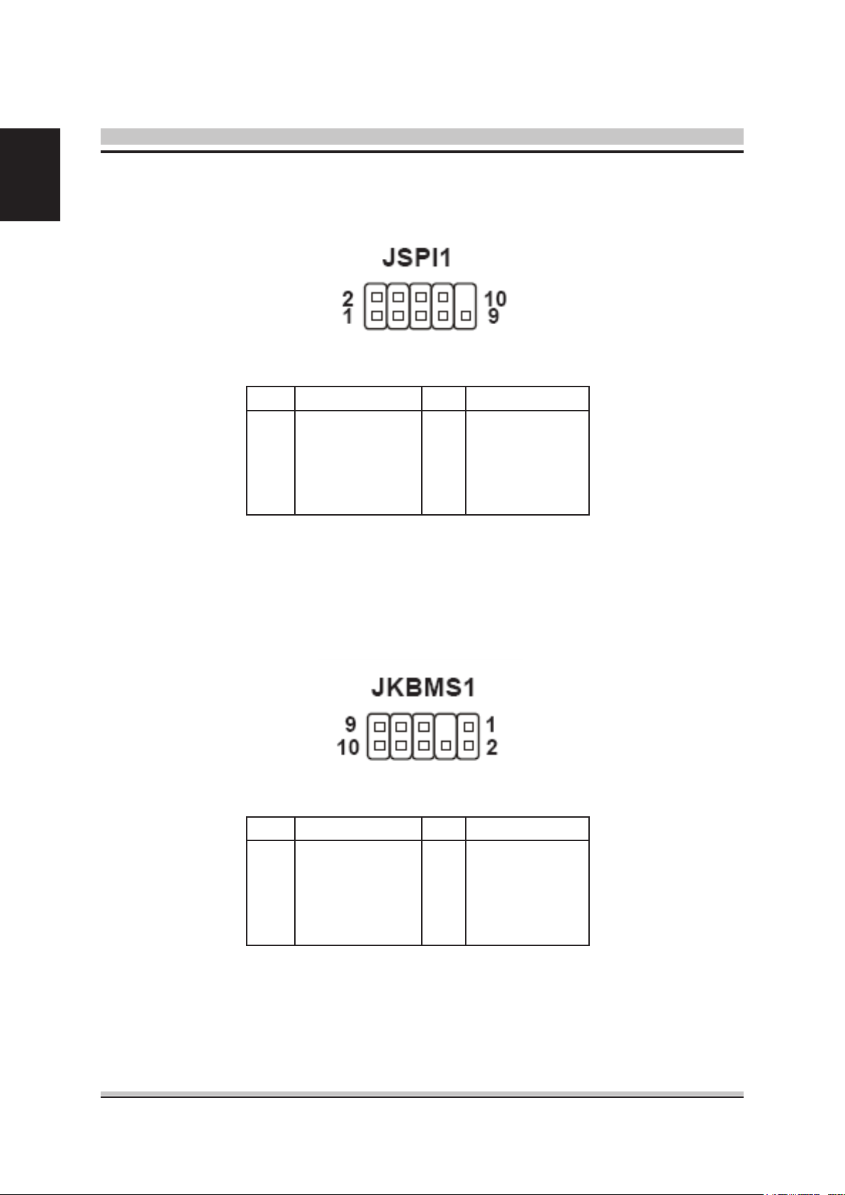
English
SPI Flash ROM Connector : JSP1
This connector is used to ash SPI ash ROM.
PIN SIGNAL PIN SINNAL
1
3
5
7
9
VCC3_SB
SPI_MISO_F
SPI_CS0_F#
GND
SPI_HOLD#
2
4
6
8
10
VCC3_SB
SPI_MOSI_F
SPI_CLK_F
GND
NC
Keyboard/Mouse Connector : JKBMS1
This connector is used to connector PS/2 keyboard & mouse.
PIN SIGNAL PIN SINNAL
1
3
5
7
9
VCC5
NC
GND
MSCLK_PH#
MSDAT_PH#
2
4
6
8
10
VCC5
NC
GND
KBCLK_PH#
KBDAT_PH#
16
Page 17
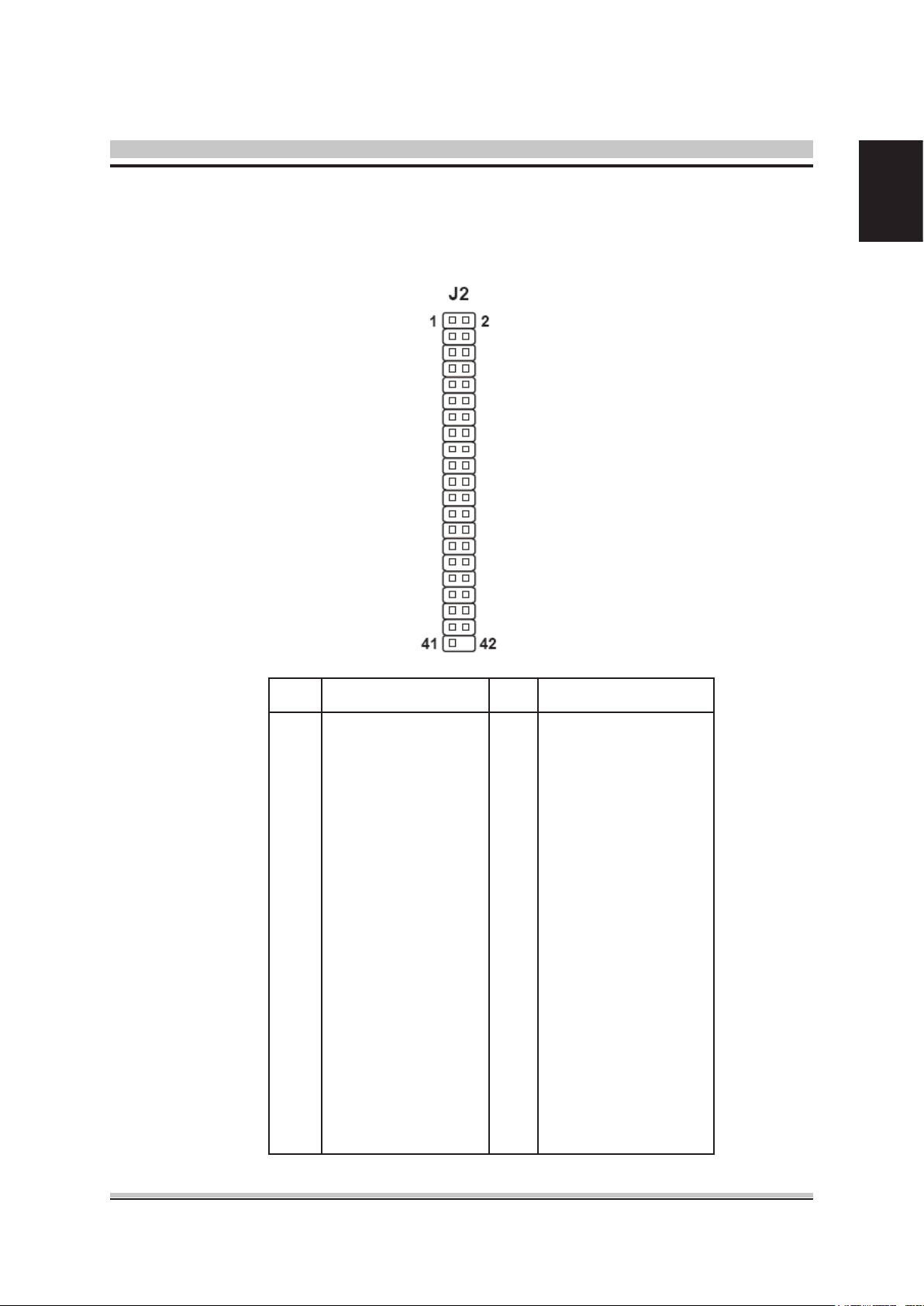
Serial Port Connector :J2
This connector is a 16550A high speed communications port that sends/receives 16
bytes FIFOs. You can attach serial devices to it through the optional serial port bracket.
English
PIN SIGNAL PIN SINNAL
1
2
3
4
5
6
7
8
9
10
11
12
13
14
15
16
17
18
19
20
COM_NDCD2
COM_NRD2
COM_NTD2
COM_NDTR2
GND
COM_NDSR2
COM_NRTS2
COM_NCTS2
VCC_COM2
No Connection
COM_NDCD3
COM_NRD3
COM_NTD3
COM_NDTR3
GND
COM_NDSR3
COM_NRTS3
COM_NCTS3
VCC_COM3
No Connection
21
22
23
24
25
26
27
28
29
30
31
32
33
34
35
36
37
38
39
40
COM_NDCD4
COM_NRD4
COM_NTD4
COM_NDTR4
GND
COM_NDSR4
COM_NRTS4
COM_NCTS4
VCC_COM4
No Connection
COM_NDCD5
COM_NRD5
COM_NTD5
COM_NDTR5
GND
COM_NDSR5
COM_NRTS5
COM_NCTS5
COM_NRI5
No Connection
17
Page 18
English
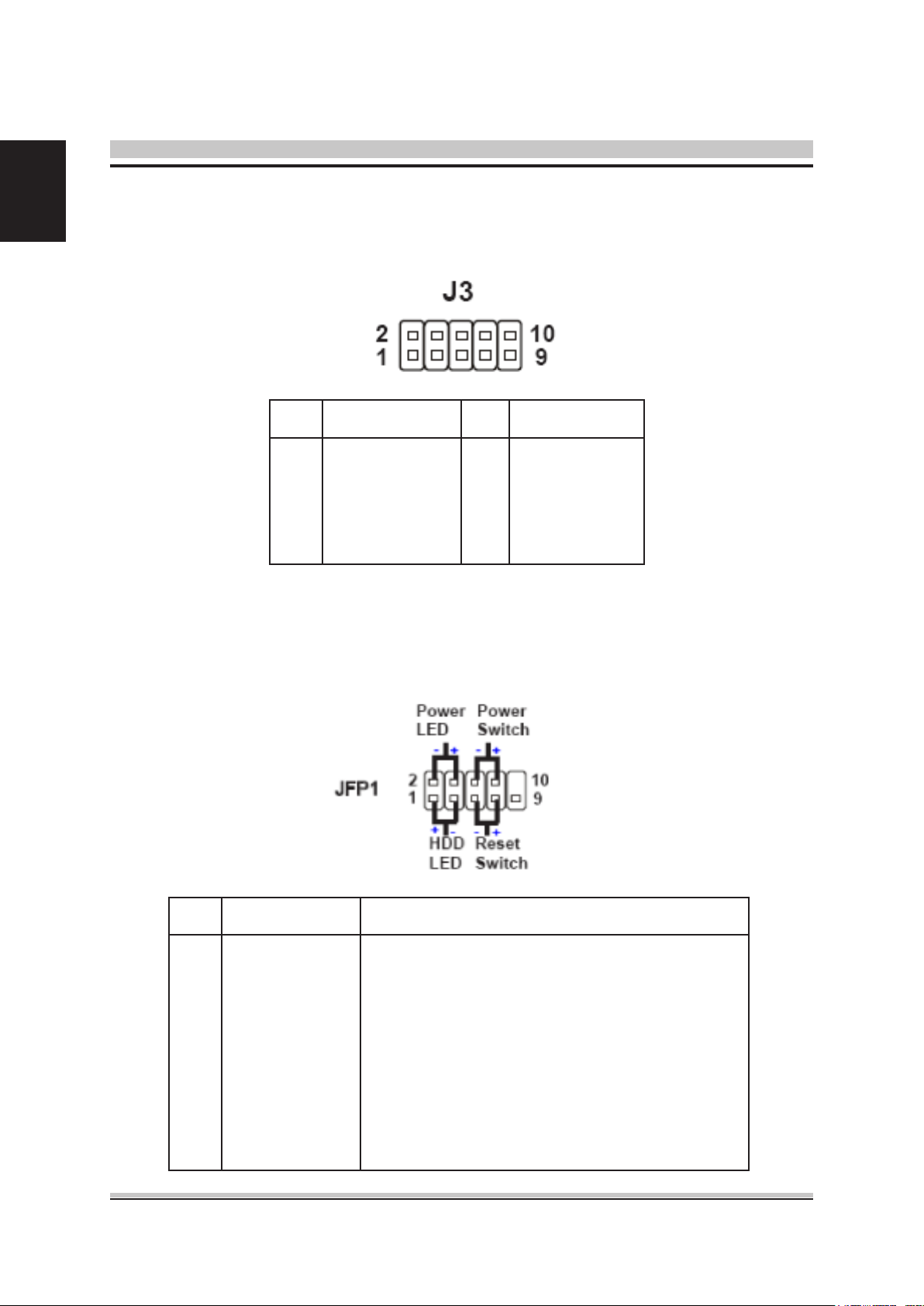
Digital IO Connector : J3
This connector is provided for the General-Purpose Input/Output (GPIO) peripheral
module.
PIN SIGNAL PIN SINNAL
1
3
5
7
9
GND
N_GPO 3
N_GPO 2
N_GPI 3
N_GPI 2
2
4
6
8
10
VCC5
N_GPO1
N_GPO 0
N_GPI 1
N_GPI 0
Front Panel Connector : JFP1
This front panel connector is provided for electrical connection to the front panel switch-
es & LEDs and is compliant with Intel Front Panel I/O Connectivity Design Guide.
18
PIN SIGNAL DESCRIPTION
1
2
3
4
5
6
7
8
9
10
HD_LED +
PWR/SLP GND
HD_LED -
FP PWR/SLP
RST_SW PWR_SW -
RST_SW +
PWR_SW +
RSVD_DNU
KEY
Hard disk LED pull-up
MSG LED pull-down to GND
Hard disk active LED
MSG LED pull-up
Reset Switch low reference pull-down to GND
Power Switch low reference pull-down to GND
Reset Switch high reference pull-up
Power Switch high reference pull-up
Reserved. Do not use.
Key
Page 19
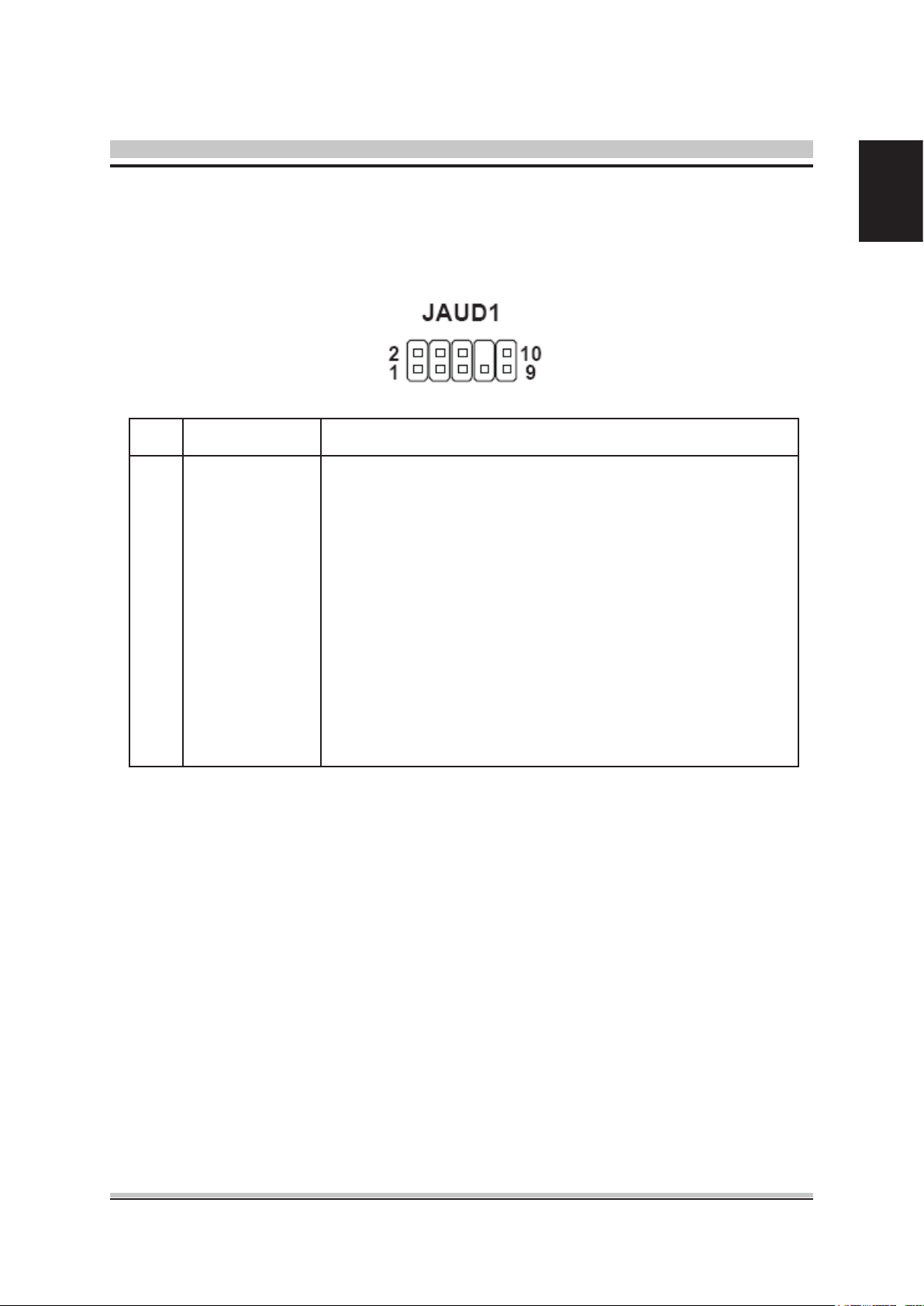
Front Panel Audio Connector : JAUD1
This connector allows you to connect the front panel audio and is compliant with Intel
Front Panel I/O Connectivity Design Guide.
PIN SIGNAL DESCRIPTION
English
1
2
3
4
5
6
7
8
9
10
MIC_L
GND
MIC_R
PRESENCE#
LINE out_R
MIC_JD
Front_JD
NC
LINE out_L
LINEout_JD
Microphone - Left channel
Ground
Microphone - Right channel
Active low signal-signals BIOS that a High Denition Audio
dongle is connected to the analog header. PRESENCE# = 0
when a High Denition Audio dongle is connected
Analog Port - Right channel
Jack detection return from front panel microphone JACK1
Jack detection sense line from the High Denition Audio
CODEC jack detection resistor network
No connection
Analog Port - Left channel
Jack detection return from front panel JACK2
19
Page 20
English
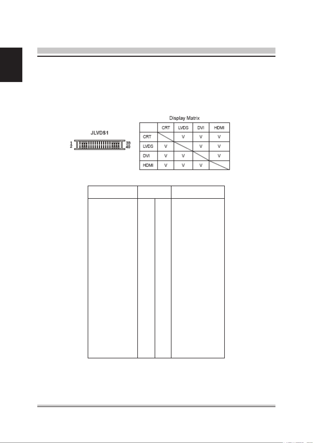
LVDS Flat Panel Connector : JLVDS1
The LVDS (Low Voltage Differential Signal) connector provides a digital interface typical-
ly used with at panels. After connecting an LVDS interfaced at panel to the JLVDS1,
be sure to check the panel datasheet and set the JVDD1 jumper (p.18) to proper power
voltage..
SIGNAL PIN SIGNAL
+12V
+12V
GND
GND
LCD_VDD
LDDC_DATA
LVDS_VDDEM
GND
LA_DATA0
LA_DATA1
LA_DATA2
LA_CLK
LA_DATA3
GND
LB_DATA0
LB_DATA1
LB_DATA2
LB_CLK
LB_DATA3
GND
2
4
6
8
10
12
14
16
18
20
22
24
26
28
30
32
34
36
38
40
1
3
5
7
9
11
13
15
17
19
21
23
25
27
29
31
33
35
37
39
+12V
+12V
+12V
VCC3/VCC5
LCD_VDD
LDDC_CLK
L_BKLTCTL
L_BKLTEM
LA_DATA0#
LA_DATA1#
LA_DATA2#
LA_CLK#
LA_DATA3#
GND
LB_DATA0#
LB_DATA1#
LB_DATA2#
LB_CLK#
LB_DATA3#
GND
20
Page 21
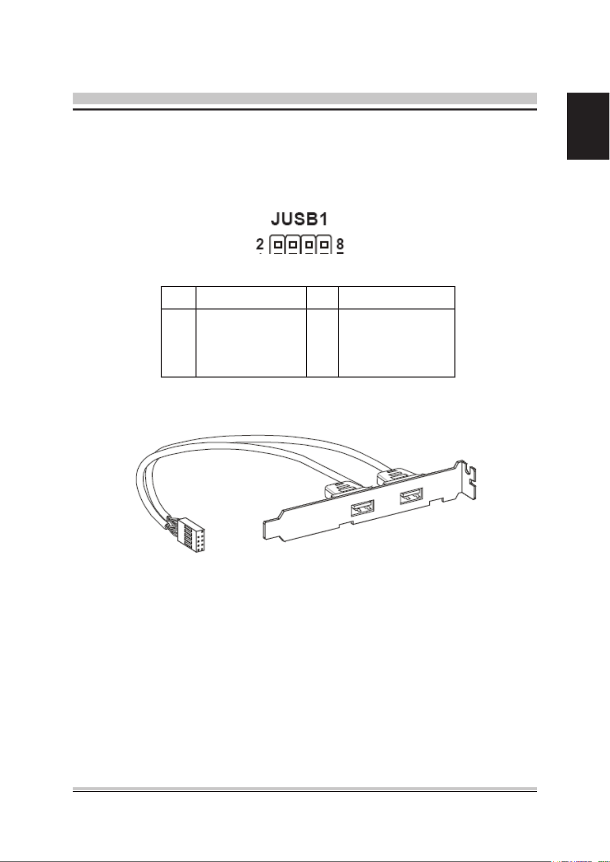
Front USB Connector : JUSB1
This connector, compliant with Intel I/O Connectivity Design Guide, is ideal for connecting high-speed USB interface peripherals such as USB HDD, digital cameras, MP3 players, modems and the like.
PIN SIGNAL PIN SINNAL
English
Important
1
3
5
7
USB_RSTR
SBD1+
SBD1GND
2
4
6
8
GND
SBD0SBD0+
USB_RSTR
USB 2.0 Bracket
(Optional)
Note that the pins of VCC and GND must be connected correctly to avoid possible dam-
age.
21
Page 22
English
1.8 Jumpers
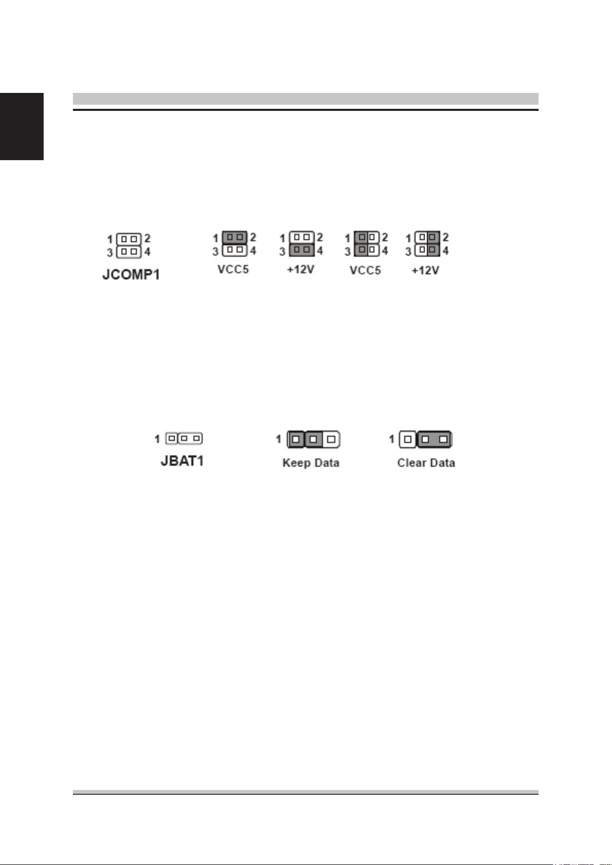
COM Port Power Jumper : JCOMP1
These jumpers specify the operation voltage of the onboard serial ports.
Clear CMOS Jumper : JBAT1
There is a CMOS RAM onboard that has a power supply from an external battery to
keep the data of system conguration. With the CMOS RAM, the system can automatically boot OS every time it is turned on. If you want to clear the system conguration, set
the jumper to clear data..
Important
You can clear CMOS by shorting 2-3 pin while the system is off. Then return to 1-2 pin
position. Avoid clearing the CMOS while the system is on; it will damage the mainboard.
22
Page 23
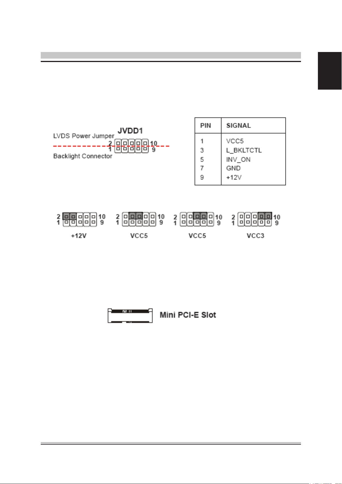
Backlight Connector & LVDS Power Jumper : JVDD1
The backlight connector is provided for LCD backlight options while the LVDS power
jumper allows users to select the operation voltage of the LVDS interfaced at panel..
English
PCI (Peripheral Component Interconnect ) Express Slot
The PCI Express slot supports the PCI Express interface expansion card.
The CON1 is a Mini PCI-E connector for wireless LAN, TV tuner, and Robson NAND
Flash.
Important
When adding or removing expansion cards, make sure that you unplug the power supply
rst. Meanwhile, read the documentation for the expansion card to congure any neces-
sary hardware or software settings for the expansion card, such as jumpers, switches or
BIOS conguration.
23
Page 24
English
2 System Installation
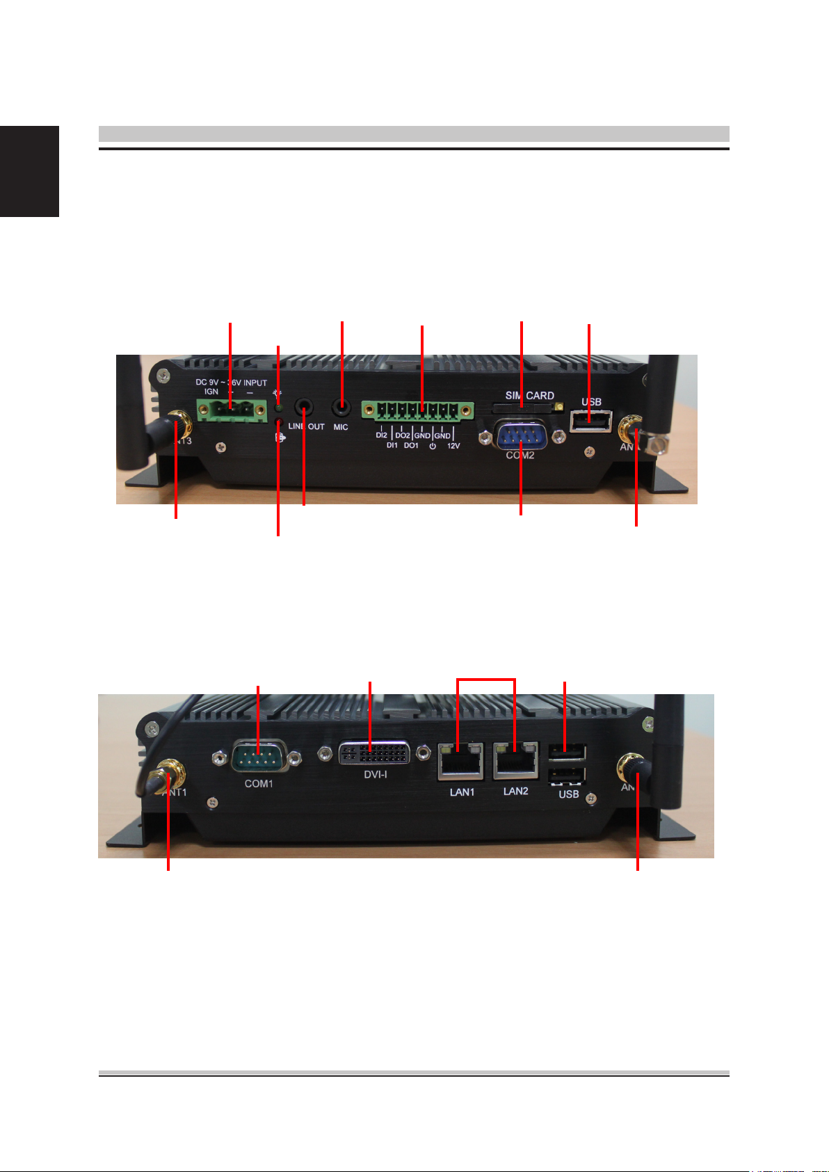
2.1 System Introduction
DC In
WIFI/BT Antenna 3
Power LED
HDD/SSD LED
COM1 Port
Line Out
Mic In
DVI
Digital I/O
LAN Port
SIM Card
COM2 Port
USB2.0 Port
USB2.0 Port
3G Antenna 4
24
GPS Antenna 1
WIFI / BT Antenna 2
Page 25
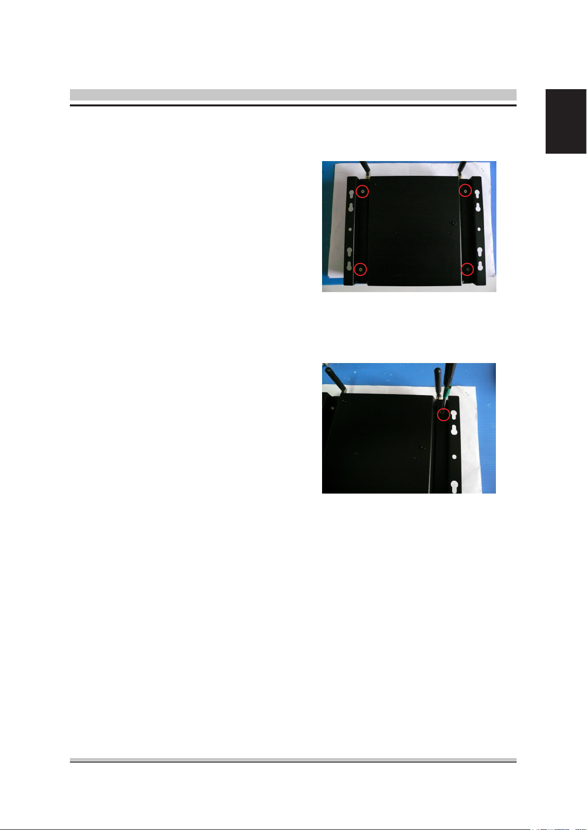
2.2 Opening Chassis with Battery Kit
English
Step 1.
in the picture.
Step 2.
back cover as shown in
the picture.
There are four screws as shown
Unscrew four screws of the
Step 3.
Open the Back Cover.
25
Page 26
English
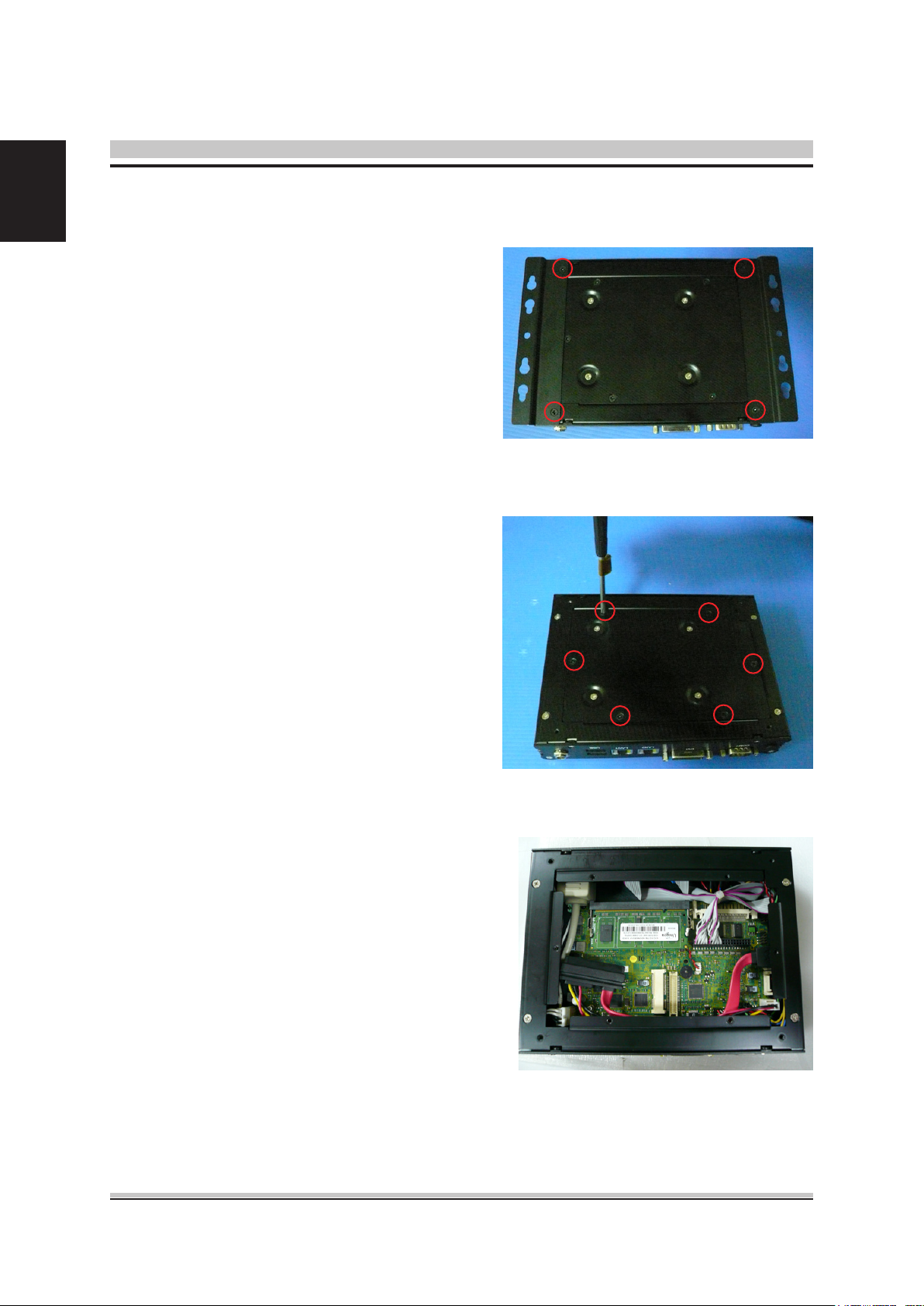
2.3 Opening Chassis without Battery Kit
Step 1.
M ounting Bracket as shown in
the picture.
Step 2.
the Back Cover as shown in
the picture.
Unscrew the four screws of the
Unscrew the six screws of
Step 3.
in the picture.
26
Open the Back Cover as shown
Page 27
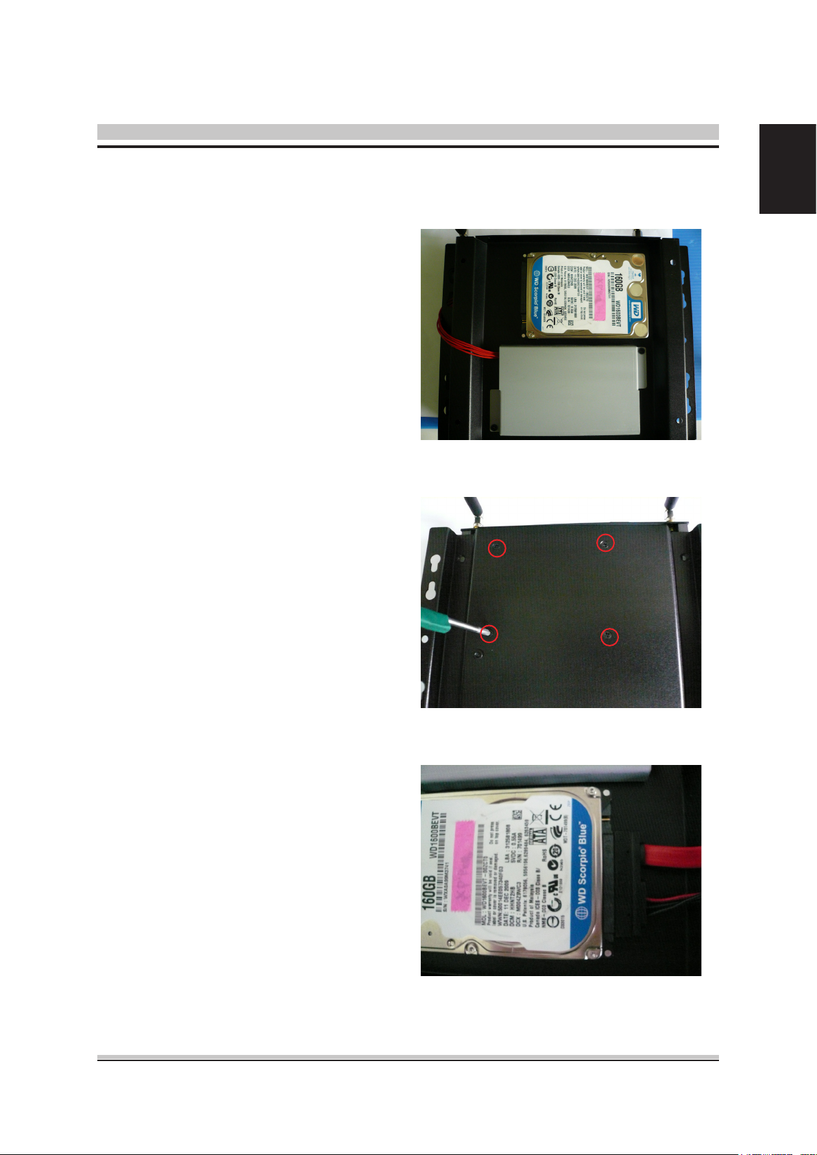
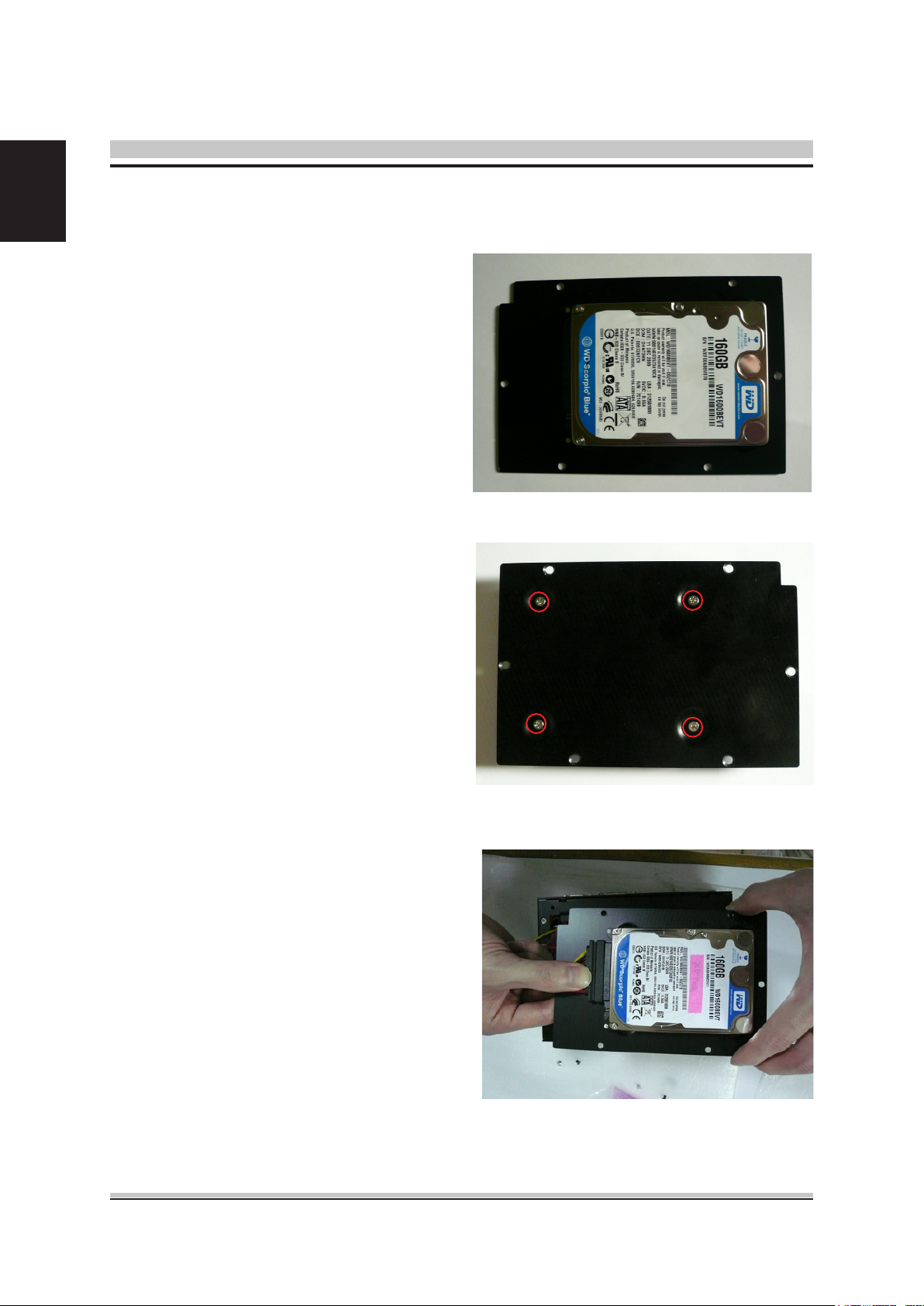
2.4 Installing HDD with Battery Kit
English
Step 1.
Cover as shown in the picture.
Step 2.
screw the four screws of the
Back Cover as shown in the
picture.
Put the HDD on the Back
Turn over the Back Cover and
Step 3.
and SATA cable to HDD as
shown in the picture.
Connect the HDD power cable
27
Page 28
English
2.5 Installing HDD without Battery Kit
Step 1.
Cover as shown in the picture.
Step 2.
screw the four screws of the
Back Cover as shown in the
picture.
Put the HDD on the Back
Turn over the Back Cover and
Step 3.
and SATA cable to HDD as
shown in the picture.
28
Connect the HDD power cable
Page 29
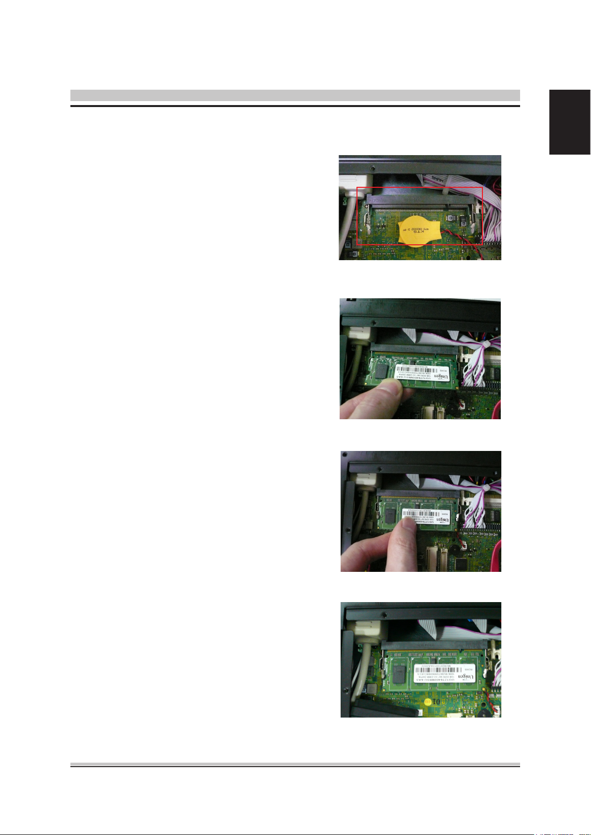
2.6 Installing Memory
English
Step 1.
in the picture.
Step 2.
aligned with the Memory socket of
the board and insert it at a 30-degree
angle into the socket as shown in
the picture.
Put Memory on this place as shown
Hold the Memory with its notch
Step 3.
socket until a “click” is heard as
shown in the picture.
Step 4.
the tabs of the socket lock on both
sides of the module as shown in the
picture.
Fully insert the module into the
Press down on the Memory so that
29
Page 30
English
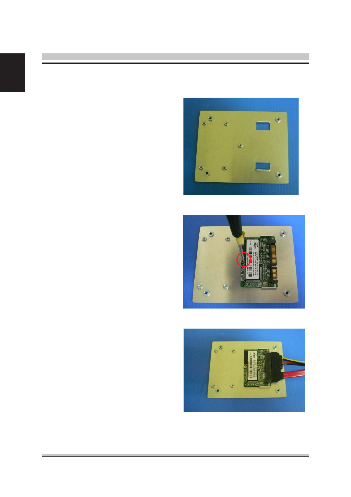
2.7 Installing SSD
Step 1.
as shown in the picture.
Step 2.
SSD holder as shown in the
picture.
Put the SSD on the bracket
Screw the one screw of the
Step 3.
and SATA cable to SSD as
shown in the picture.
Step 4.
30
Connect the SSD power cable
See
2.5 Installing HDD
Page 31
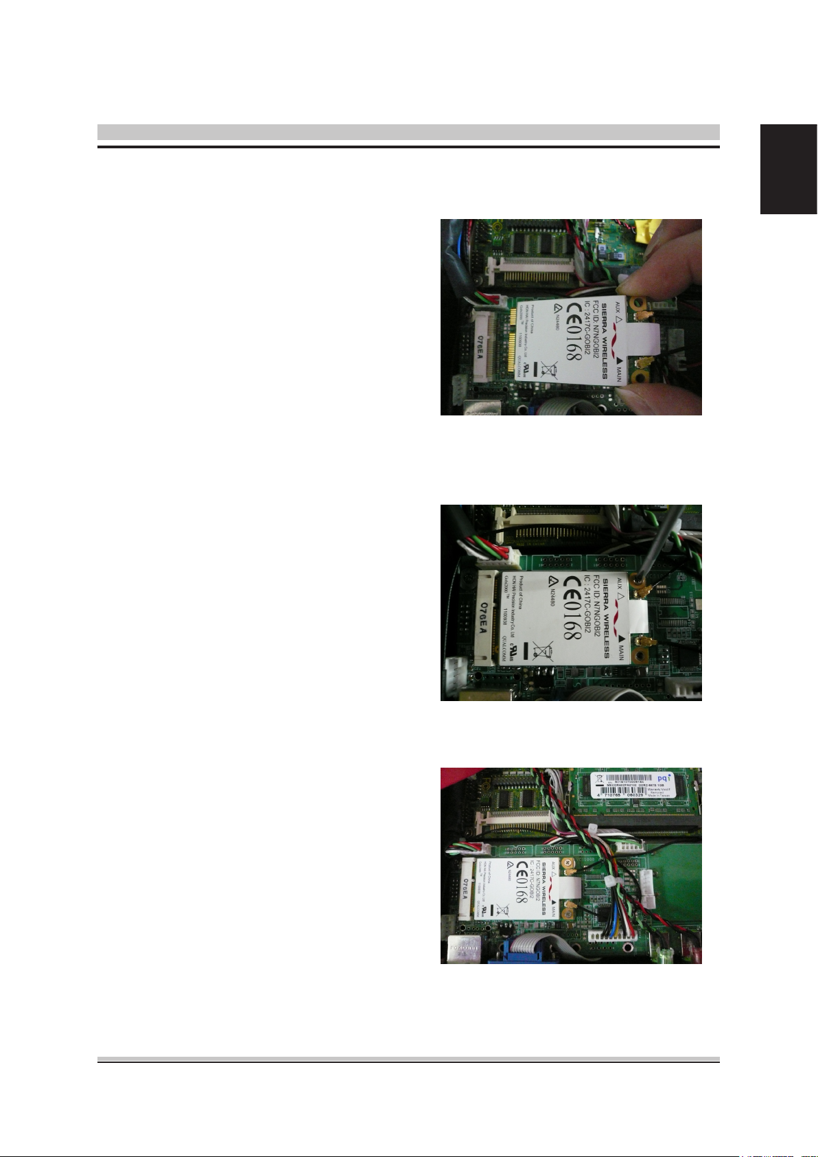
2.8 Installing 3G Module
English
Step 1.
aligned with the socket of the
board and insert it at a 30
degree angle into the socket as
shown in the picture.
Step 2.
as shown in the picture.
Hold the Module with its notch
Screw one screw to the holder
Step 3.
picture.
Done as shown in the
31
Page 32
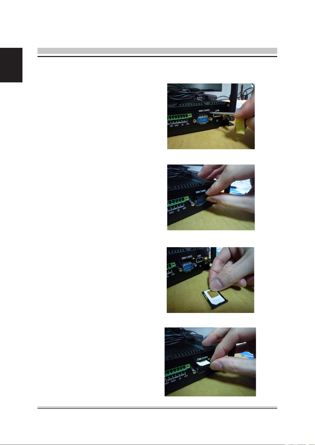
English
2.9 Installing SIM Card
Step 1.
as shown in the picture.
Step 2.
VBOX-3000 as shown in the
picture.
Use thin stick to push the button
Take the holder away from
Step 3.
as shown in the picture.
Step 4.
Insert it into the socket as
shown in the picture.
Step 5.
Put your SIM Card into the holder
Take the SIM card holder and
Done.
32
Page 33
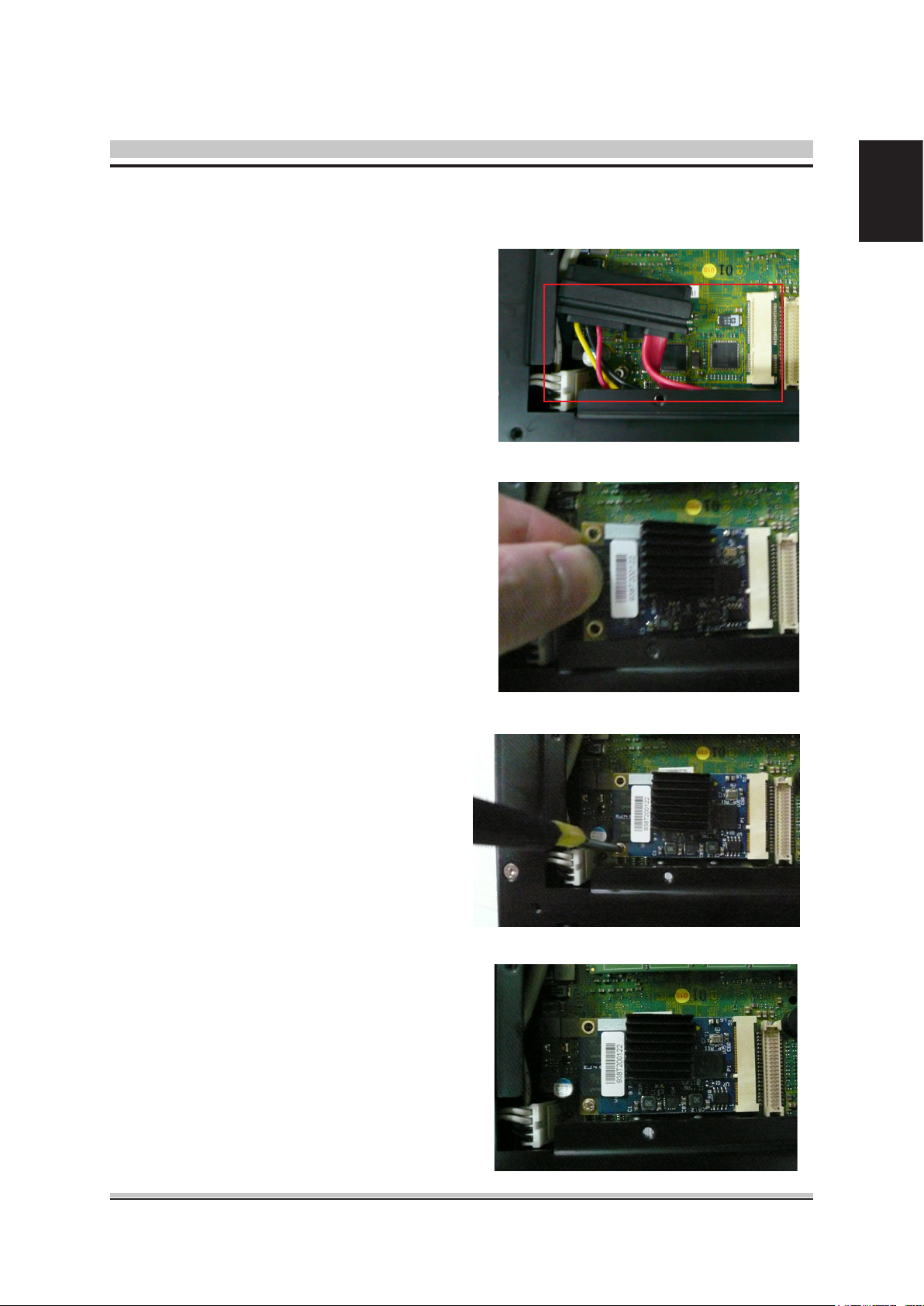
2.10 Installing MINI PCI Express Expansion Card (WiFi Module)
English
Step 1.
on this place as shown in the
picture.
Step 2.
aligned with the socket of the
board and insert it at a 30
degree angle into the socket as
shown in the picture.
Put MINI PCIe Expansion Card
Hold the Module with its notch
Step 3.
as shown in the picture.
Step 4.
picture.
Screw one screw to the holder
Done as shown in the
33
Page 34
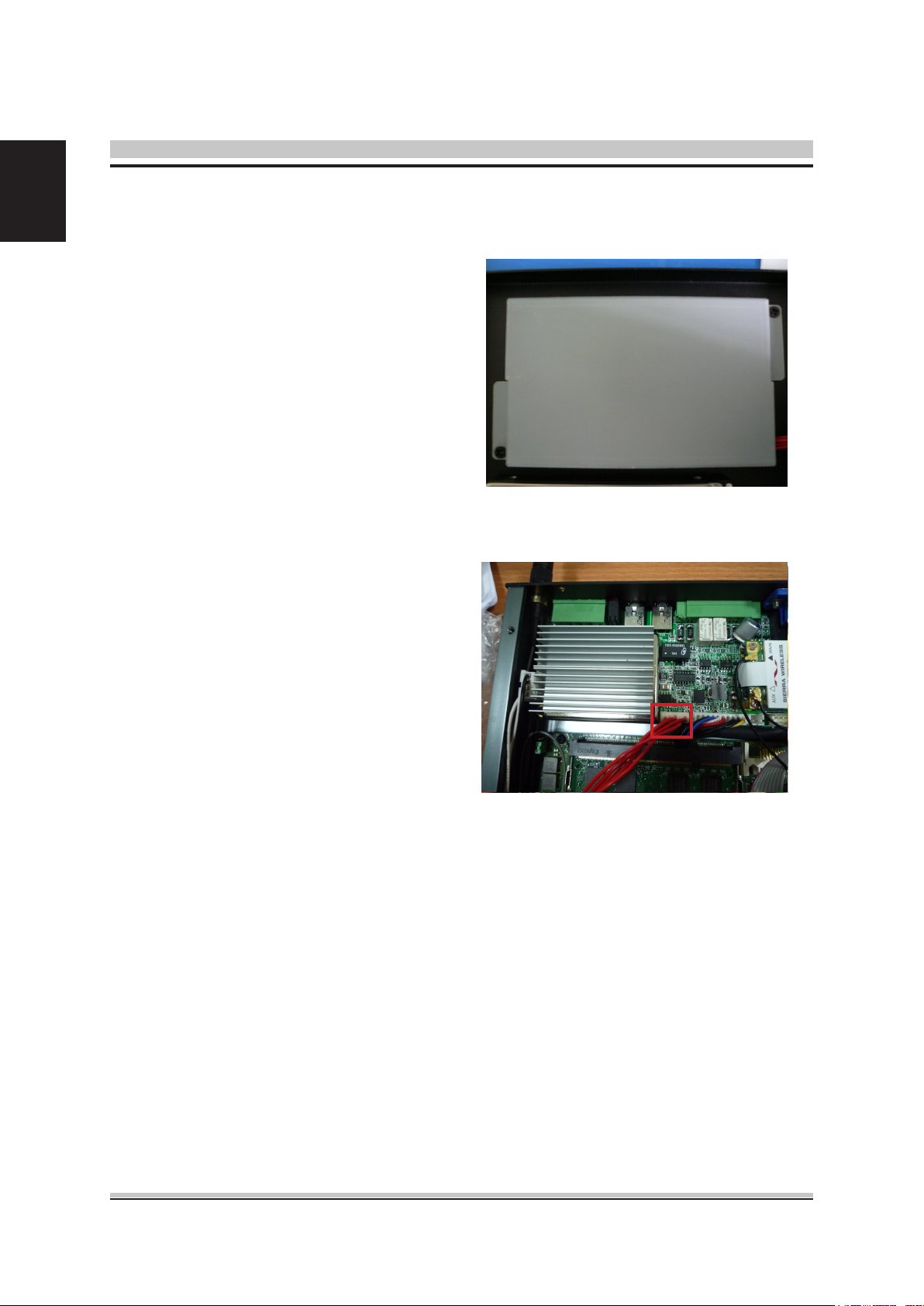
English
2.11 Installing Battery Module
Step 1.
back cover as shown
in the picture.
Step 2.
Connector as shown in the
picture.
Screw two screws on the
Connect the Cable to UPS1
34
Page 35

3 BIOS
3.1 Entering The BIOS
Power on the computer and the system will start POST (Power On Self Test) process.
When the message below appears on the screen, press (DEL) key to enter Setup.
Press DEL to enter SETUP
If the message disappears before you respond and you still wish to enter Setup, restart
the system by turning it OFF and On or pressing the RESET button. You may also restart
the system by simultaneously pressing <Ctrl>, <Alt>, and <Delete> keys.
Important
• The items under each BIOS category described in this chapter are under continuous
update for better system performance. Therefore, the description may be slightly different from the latest BIOS and should be held for reference only.
• Upon boot-up, the 1st line appearing after the memory count is the BIOS version. It is
usually in the format.
English
VBOX-3000 Mainboard V1.0 073109 where :
1st digit refers to BIOS maker as A = AMI, W = AWARD, and P = PHOENIX
2nd - 5th digit refers to the model number.
6th digit refers to the chipset as I = Intel, N = NVIDIA, A = AMD and V = VIA.
7th - 8th digit refers to the customer as MS = all standard customers.
V1.0 refers to the BIOS was released.
073109 refers to the date this BIOS was released.
35
Page 36
English
Control Keys
Power on the computer and the system will start POST (Power On Self Test) process.
When the message below appears on the screen, press (DEL) key to enter Setup.
<↑> Move to the previous item
<↓> Move to the next item
<←> Move to the item in the left hand
<→> Move to the item in the right hand
<Enter> Select the item
<Esc> Jumps to the Exit menu or returns to the main menu from a submenu
<+/PU> Increase the numeric value or make changes
<-/PD> Decrease the numeric value or make changes
<F1> General Help
<F9> Load Optimized Defaults
<F8> Load Fail-Safe Defaults
<F10> Save all the CMOS changes and exit
Getting Help
After entering the Setup menu, the rst menu you will see is the Main Menu.
Main Menu
The main menu lists the setup functions you can make changes to. You can use the
arrow keys (↑↓) to select the item. The on-line description of the highlighted setup function is displayed at the bottom of the screen.
Sub-Menu
If you nd a right pointer symbol (as shown in the right view) appears to the left of certain elds that means a sub-menu can be launched from this eld. A sub-menu contains additional options for a eld parameter. You can use arrow keys ( ↑↓ ) to highlight
the eld and press <Enter> to call up the sub-menu. Then you can use the control keys
to enter values and move from eld to eld within a sub-menu. If you want to return to
the main menu, just press the <Esc >.
General Help <F1>
The BIOS setup program provides a General Help screen. You can call up this screen
from any menu by simply pressing <F1>. The Help screen lists the appropriate keys to
use and the possible selections for the highlighted item. Press <Esc> to exit the Help
screen.
36
Page 37
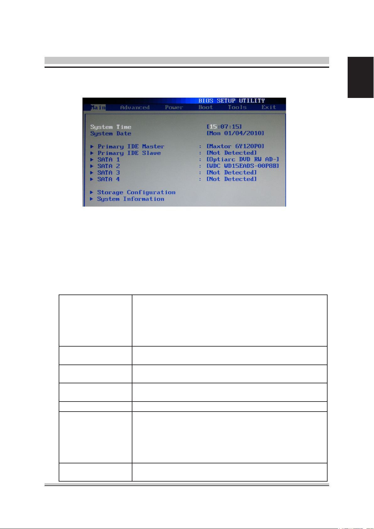
3.2 Main
System Time
This setting allows you to set the system time. The time format is <Hour> <Minute>
<Second>.
System Date
This setting allows you to set the system Date. The time format is <Day> <Month> <Date>
<Year>.
English
Primary IDE Master/Slave, SATA 1/2
[Type] Press PgUp/<+> or PgDn/<-> to select
[Manual], [None] or [Auto] type. Note that the specications
of your drive must match with the drive table. The hard disk
will not work properly if you enter improper information for this
category. If your hard disk drive type is not matched or listed,
you can use [Manual] to dene your own drive type manually.
[LBA/Large Mode] Enabling LBA causes Logical Block Addressing to be used in
place of Cylinders, Heads and Sectors.
[Block (Multi-Sector
Transfer)]
[PIO Mode] Indicates the type of PIO (Programmed
[DMA Mode] Indicates the type of Ultra DMA
[S.M.A.R.T.] This allows you to activate the S.M.A.R.T.
[32 Bit Data Transfer] Enables 32-bit communication between
Any selection except Disabled determines the number of sectors transferred per block.
Input/Output)
(Self-Monitoring Analysis & Reporting Technology) capability for the hard disks. S.M.A.R.T is a utility that monitors your
disk status to predict hard disk failure. This gives you an opportunity to move data from a hard disk that is going to fail to
a safe place before the hard disk becomes ofine.
CPU and IDE controller
37
Page 38
English
3.3 Advanced
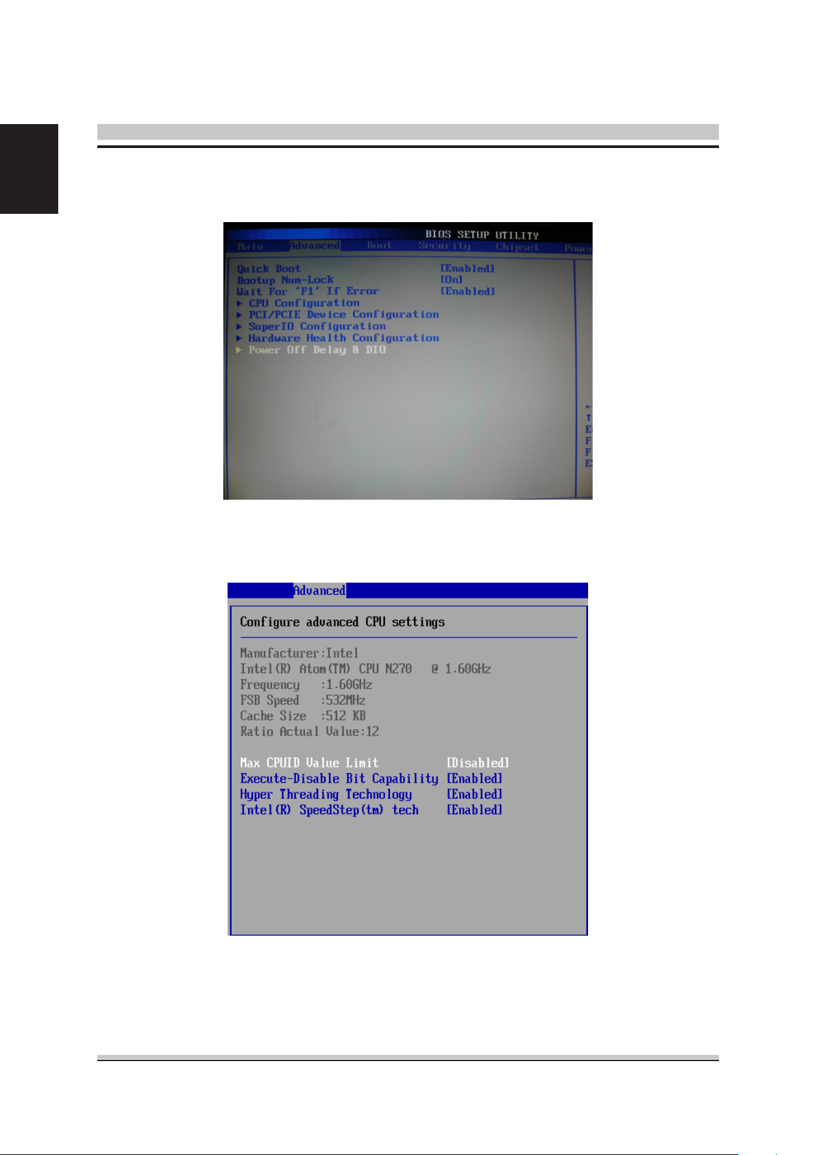
CPU Configuration
38
Page 39

» Max CPUID Value Limit
The Max CPUID Value Limit BIOS feature allows you to circumvent problems with older
operating systems that do not support the Intel Pentium 4 processor with Hyper-Threading
Technology. When enabled, the processor will limit the maximum CPUID input value to
03h when queried, even if the processor supports a higher CPUID input value. When
disabled, the processor will return the actual maximum CPUID input value of the processor when queried.
» Execute Disable Bit Capability
Intel’s Execute Disable Bit functionality can prevent certain classes of malicious “buffer
overow” attacks when combined with a supporting operating system. This functionality
allows the processor to classify areas in memory by where application code can execute
and where it cannot. When a malicious worm attempts to insert code in the buffer, the
processor disables code execution, preventing damage or worm propagation.
» Hyper Threading Technology
The processor uses Hyper Threading technology to increase transaction rates and reduces
end-user response times. The technology treats the two cores inside the processor as two
logical processors that can execute instructions simultaneously. In this way, the system
performance is highly improved. If you disable the function, the processor will use only
one core to execute the instructions. Please disable this item if your operating system
doesn’t support HT Function, or unreliability and instability may occur.
English
» Intel(R) SpeedStep(tm) Tech
EIST (Enhanced Intel SpeedStep Technology) allows the system to dynamically adjust
processor voltage and core frequency, which can result in decreased average power
consumption and decreased average heat production..
39
Page 40
English
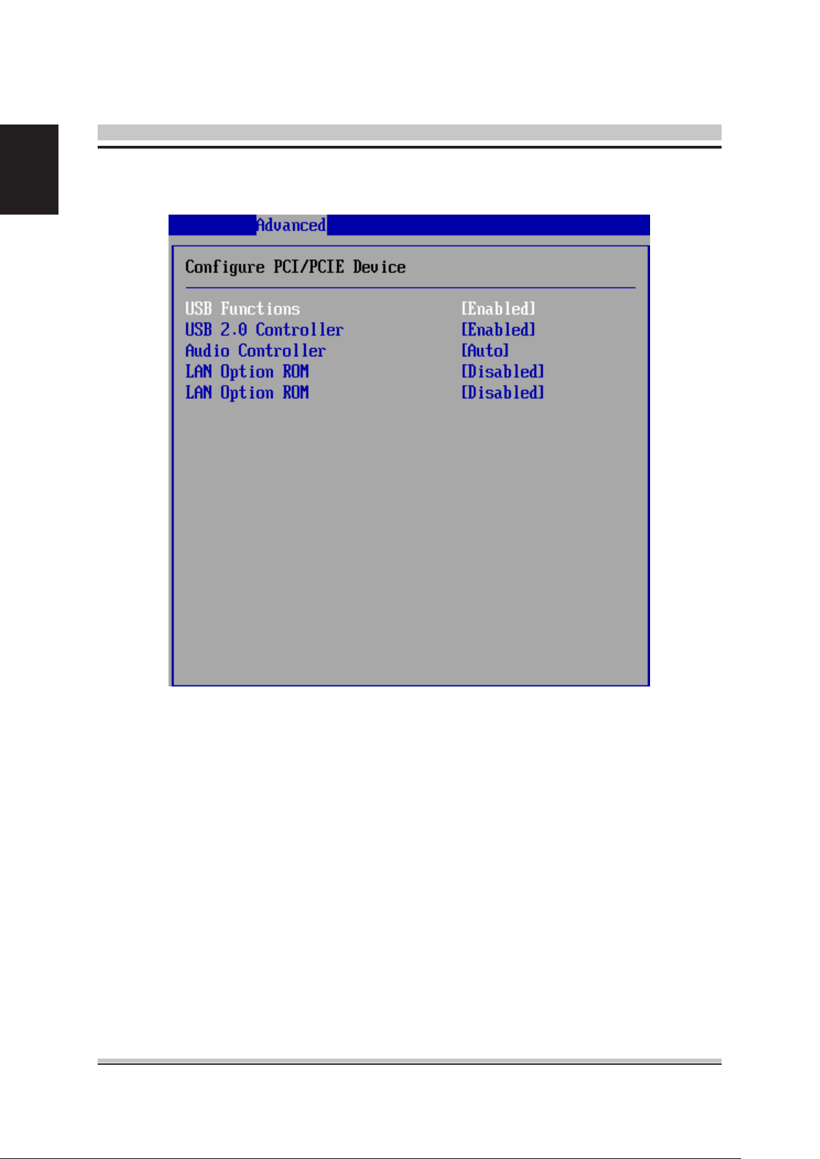
PCI/ PCIE Device Configuration
» USB Functions
This setting species the operation mode of the onboard USB controller.
» USB 2.0 Controller
This setting enables/disables the onboard USB controller.
» Audio Controller
This setting enables / disable the onboard USB controller.
» LAN Option ROM
The items enable or disable the initiation of the onboard LAN Boot ROMs during bootup.
Selecting [Disabled] will speed up the boot process.
40
Page 41
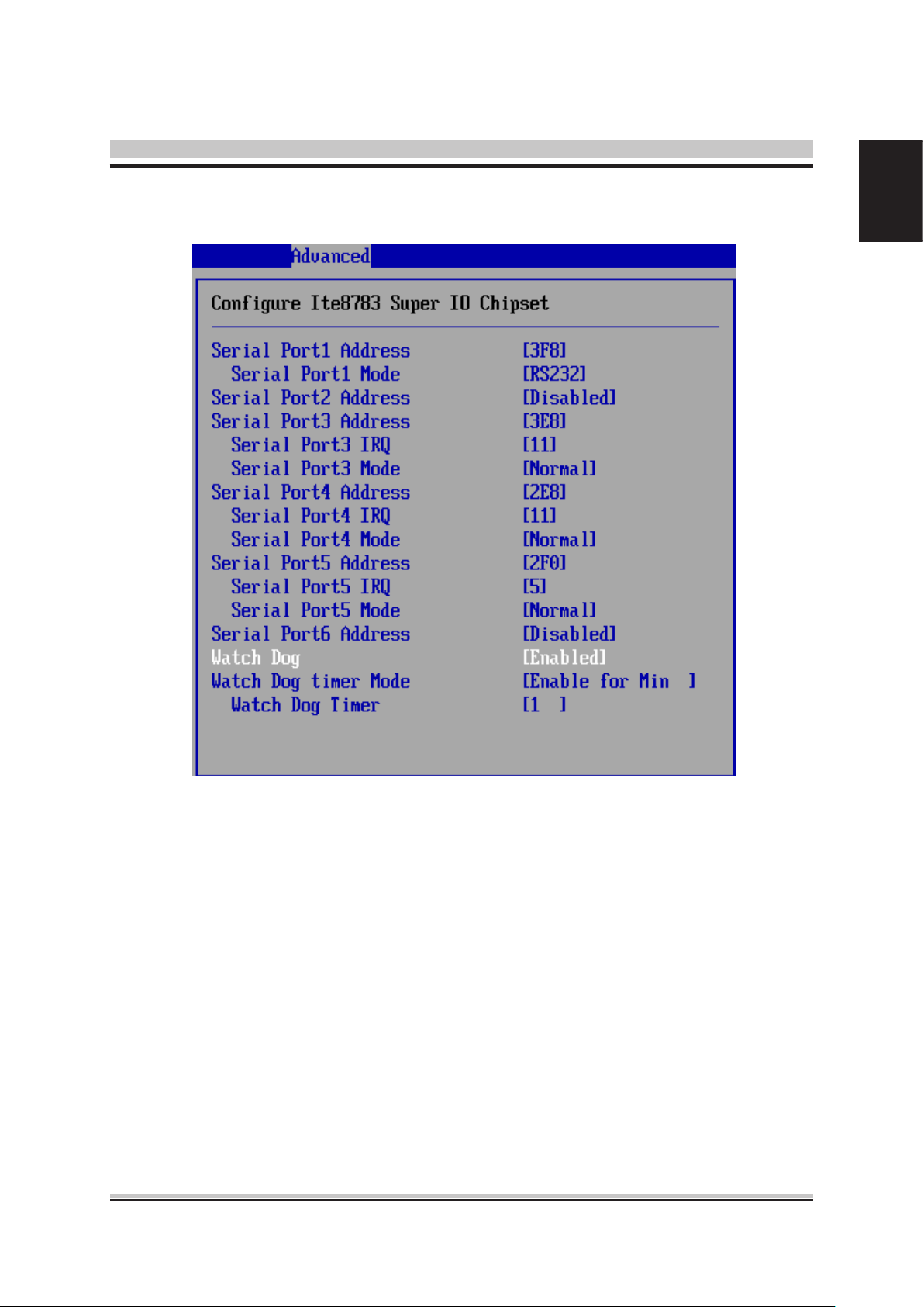
Super IO Configuration
English
» Serial Port 1/2/3/4/5/6 Address, Serial Port 3/4/5 IRQ
Select an address and a corresponding interrupt for the specied serial ports.
» Serial Port 3/4/5 Mode
These settings specify the operation mode of the specied serial prots.
» Watch Dog
You can enable the system watch-dog timer, a heardware timer that generates either an
NMI or a reset when the software that it monitors does not respond as expected each
time the watch Dog Timer action.
» Watch Dog Timer Mode
The setting species the Watch Dog Timer action.
» Watch Dog Timer
The setting species the Watch Dog Timer time out value.
41
Page 42
English
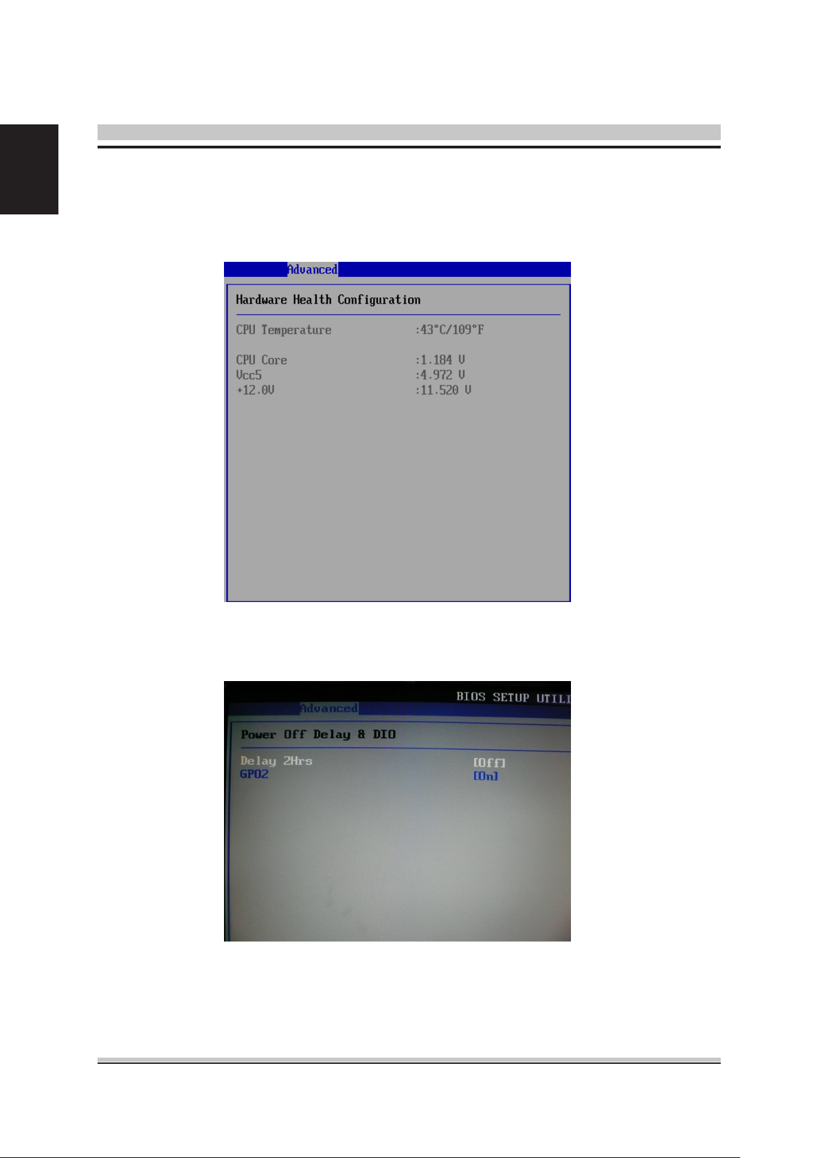
Hardware Health Configuration
These items display the current status of all monitored hardware devices/components such
as voltages, temperatures and all fans' speeds.
Power off Delay Time & DIO Configuration
» Power-off delay time is selectable by BIOS to disable and enable in 5 min / 2Hrs.
GPO Setting congure special GPO data.
42
Page 43
3.4 Boot
English
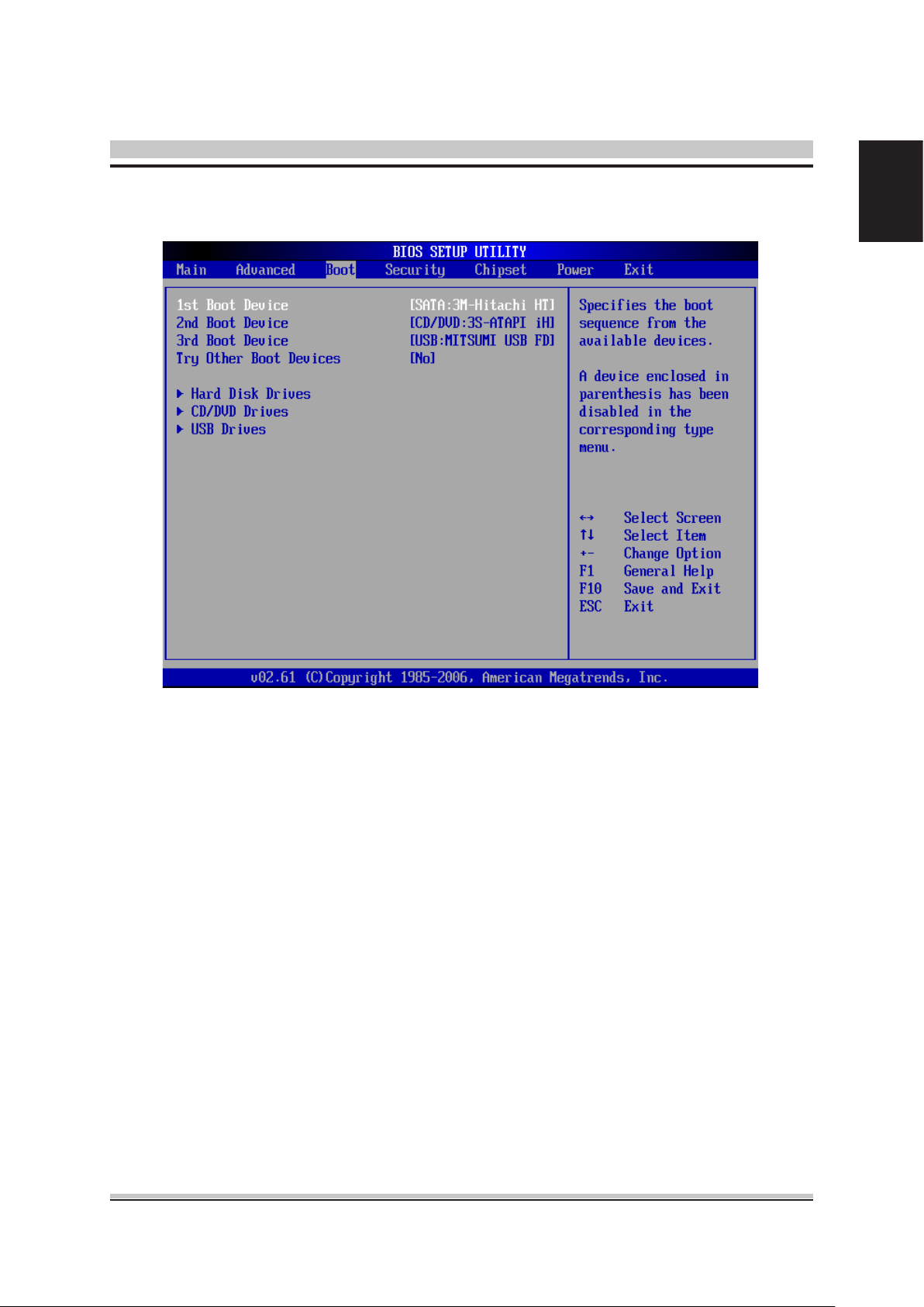
» 1st/2nd/3rd Boot Device
The items allow you to set the sequence of boot devices where BIOS attempts to load
the disk operating system.
» Try Other Boot Devices
Setting the option to [Enabled] allows the system to try to boot from other device if the
system fail to boot from the 1st/2nd/3rd boot device.
» Hard Disk Drives, CD/DVD Drives, USB Drives
These settings allow you to set the boot sequence of the specied devices.
43
Page 44
English
3.5 Security
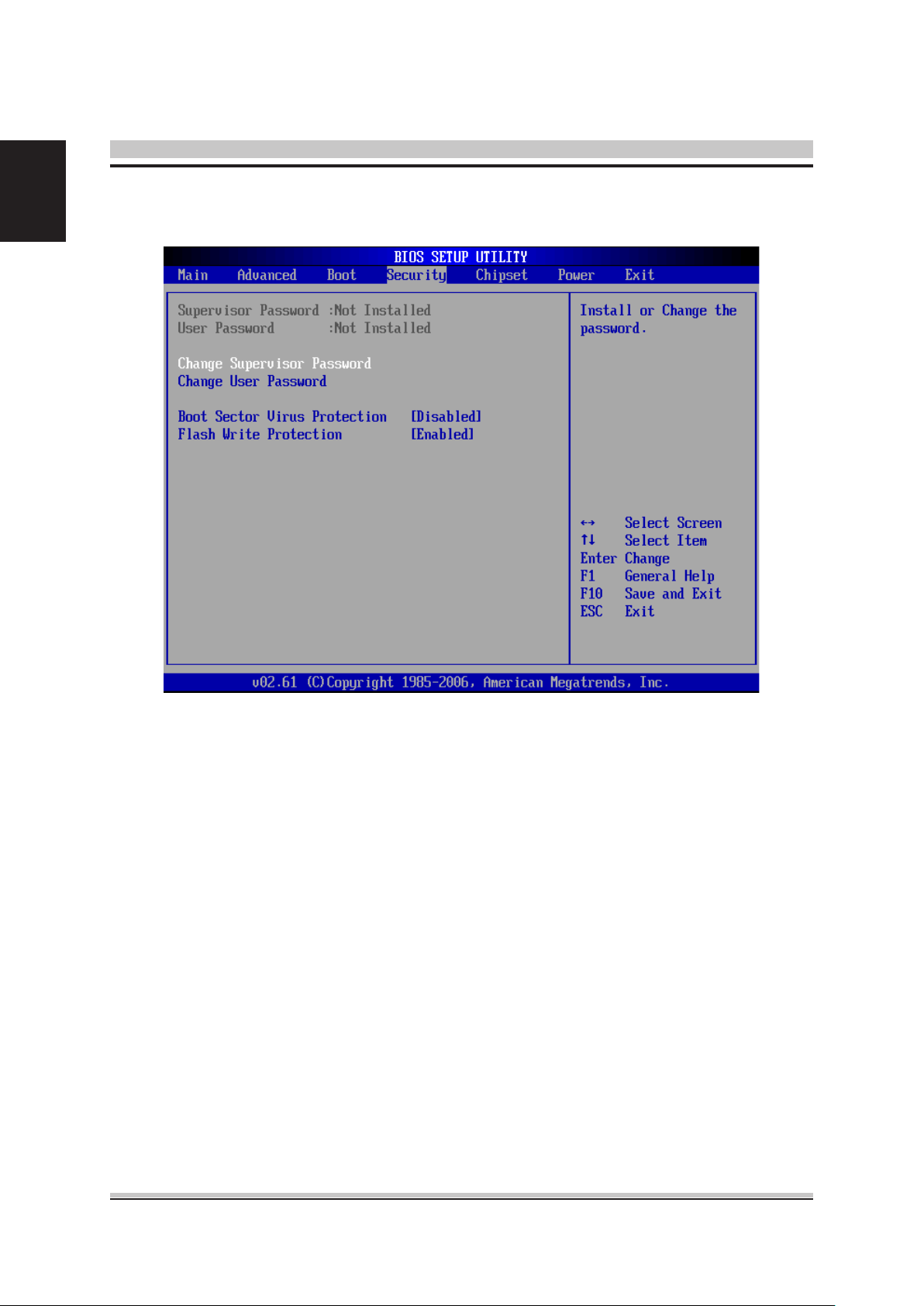
» Supervisor Password / Change Supervisor Password
Supervisor Password controls access to the BIOS Setup utility. These settings allow you
to set or change the supervisor password.
» User Password / Change User Password
User Password controls access to the system at boot. These settings allow you to set or
change the user password.
» Boot Sector Virus Protection
This function protects the BIOS from accidental corruption by unauthorized users or
computer viruses. When enabled, the BIOS data cannot be changed when attempting to
update the BIOS with a Flash utility. To successfully update the BIOS, you will need to
disable this Flash Protection function.
44
Page 45
3.6 Chipset
English
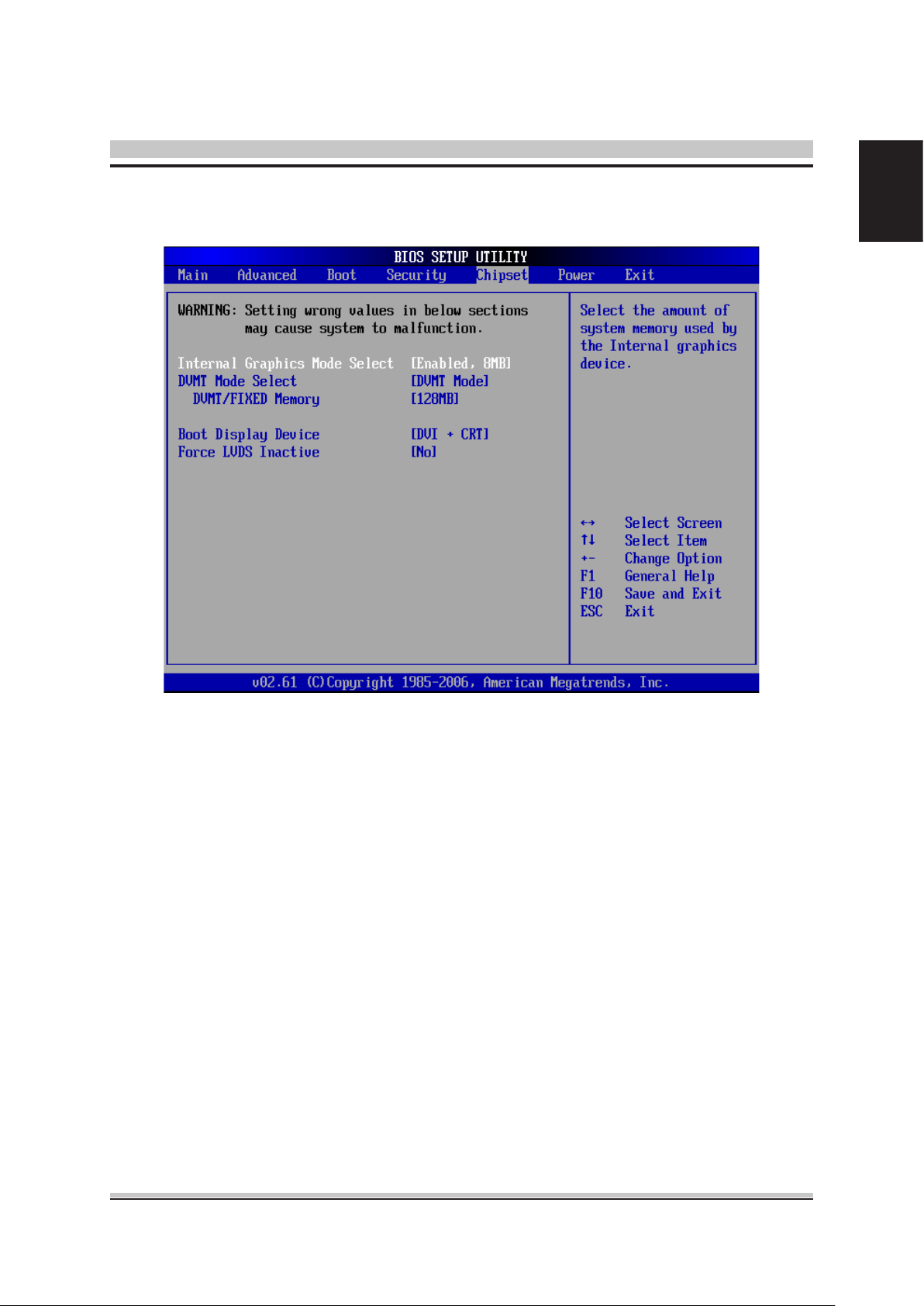
» Internal Graphics Mode Select
The eld species the size of system memory allocated for video memory.
» DVMT Mode Select
Intel's Dynamic Video Memory Technology (DVMT) allows the system to dynamically allocate memory resources according to the demands of the system at any point in time. The
key idea in DVMT is to improve the efciency of the memory allocated to either system
or graphics processor.
DVMT/FIXED Memory
When set to DVMT/FIXED Mode, the graphics driver will allocate a xed amount of
memory as dedicated graphics memory, as well as allow more system memory to
be dynamically allocated between the graphics processor and the operating system.
» Boot Display Device
Use the eld to select the type of device you want to use as the display(s) of the system.
» Force LVDS Inactive
This setting determines whether to force the LVDS inactive or not.
45
Page 46
English
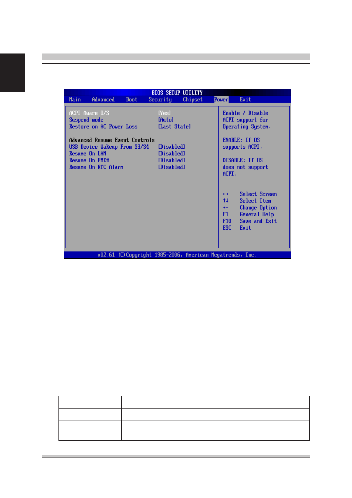
3.7 Power
» ACPI Aware O/S
This setting enables/disables ACPI (Advanced Conguration and Power Interface) support for Operating System. Set to [No] if your OS doesn’t support ACPI and set to [Yes]
if ACPI is supported.
» Suspend Mode
This item species the power saving modes for ACPI function. If your operating system
supports ACPI, you can choose to enter the Standby mode in S1 (POS) or S3 (STR)
fashion through the setting of this eld.
» Restore on AC Power Loss
This setting species whether your system will reboot after a power failure or interrupt
occurs. Available settings are:
[Power Off] Leaves the computer in the power off state.
[Power On] Leaves the computer in the power on state.
[Last State]
Restores the system to the previous status before power failure
or interrupt occured.
46
Page 47

» USB Device Wakeup From S3/S4
This setting allows the activity of the USB device to wake up the system from the S3/S4
sleep state.
» Resume On LAN
This eld species whether the system will be awadened from power saving modes when
activity or input signal of onboard LAN is detected..
» Resume On PME#
When setting to [Enabled], the feature allows your system to be awakended from the
power saving modes through any event on PME (Power management Event):
» Resume On RTC Alarm
When [Enable], you can set the date and time at which the RTC (Real-Time Clock) alarm
awakens the system from suspend mode.
English
47
Page 48
English
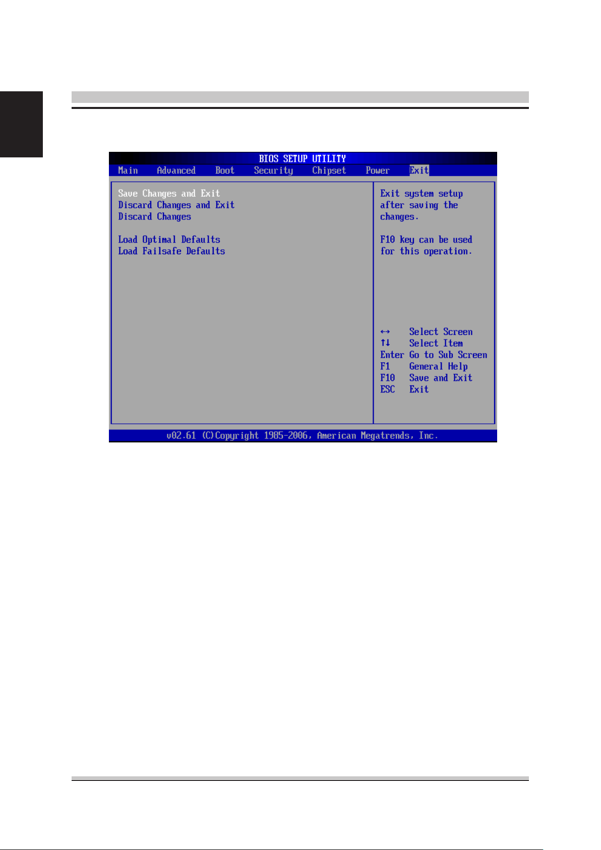
3.8 Exit
» Save Changes and Exit
Save changes to CMOS and exit the Setup Utility.
» Discard Changes and EXit
Abandon all changes and exit the Setup Utility.
» Discard Changes
Abandon all changes and continue with the Setup Utility.
» Load Optimal Defaults
Use this menu to load the default values set by the mainboard manufacturer specically
for optimal performance of the mainboard.
» Load Failsafe Defaults
Use this menu to load the default values set by the BIOS vendor for stable system performance.
48
Page 49

4 System Resources
4.1 Watch Dog Timer Setting
Software code
SIO_IDX equ 2Eh
SIO_DTA equ 2Fh
Timer equ 10; reset after 10 seconds
1. Enter conguration mode
mov dx,SIO_IDX
mov al,87h
out dx,al
mov al,01h
out dx,al
mov al,55h
out dx,al
out dx,al
2. Set to LDN 07
mov dx,SIO_IDX
mov al,07h
out dx,al
mov dx,SIO_DTA
mov al,07h
out dx,al
English
3. Set WatchDog Timer
mov dx,SIO_IDX
mov al,073h
out dx,al
mov dx,SIO_DTA
mov al,Timer
out dx,al
4. Exit conguration mode
mov dx,SIO_IDX
mov al,02h
out dx,al
mov dx,SIO_DTA
out dx,al
49
Page 50

English
4.2 GPIO Setting
; Read GPI0-GPI3 DATA
mov dx, 0a25h
in al, dx ; al = GPI0-GPI7 data
; BIT7=GPI7, BIT6=GPI6, BIT5=GPI5, BIT4=GPI4
; BIT3=GPI3, BIT2=GPI2, BIT1=GPI1, BIT0=GPI0
; Write GPO0-GPO3
mov dx, 0a25h
in al, dx
or al, 11110000h ; Set GPO0-GPO3 = High
and al, 00001111h ; Set GPO0-GPO3 = Low
out dx, al
50
Page 51

4.3 AMI Post Code
» Bootblock Initialization Code Checkpoints
The Bootblock initialization code sets up the chipset, memory and other components before
system memory is available. The following table describes the type of checkpoints that may
occur during the bootblock initialization portion of the BIOS:
Checkpoint Description
English
Before D1
D1
D0
D2
D3
D4
D5
D6
D7
D8
D9
DA Restore CPUID value back into register. Give control to BIOS POST
Early chipset initialization is done. Early super I/O initialization is
done including RTC and keyboard controller. NMI is disabled.
Perform keyboard controller BAT test. Check if waking up from
power management suspend state. Save power-on CPUID value in
scratch CMOS.
Go to at mode with 4GB limit and GA20 enabled. Verify the bootblock checksum.
Disable CACHE before memory detection. Execute full memory siz-
ing module. Verify that at mode is enabled.
If memory sizing module not executed, start memory refresh and do
memory sizing in Bootblock code. Do additional chipset initialization.
Re-enable CACHE. Verify that at mode is enabled.
Test base 512KB memory. Adjust policies and cache rst 8MB. Set
stack.
Bootblock code is copied from ROM to lower system memory and
control is given to it. BIOS now executes out of RAM.
Both key sequence and OEM specic method is checked to deter-
mine if BIOS recovery is forced. Main BIOS checksum is tested. If
BIOS recovery is necessary, control ows to checkpoint E0. See
Bootblock Recovery Code Checkpoints section of document for
more information.
Restore CPUID value back into register. The Bootblock-Runtime
interface module is moved to system memory and control is given to
it. Determine whether to execute serial ash.
The Runtime module is uncompressed into memory. CPUID information is stored in memory.
Store the Uncompressed pointer for future use in PMM. Copying
Main BIOS into memory. Leaves all RAM below 1MB Read-Write
including E000 and F000 shadow areas but closing SMRAM.
(ExecutePOSTKernel). See POST Code Checkpoints section of
document for more information.
51
Page 52

English
» POST Code Checkpoins
The POST code checkpoints are the largest set of checkpoints during the BIOS pre-boot
process. The following table describes the type of checkpoints that may occur during the
POST portion of the BIOS:
Checkpoint Description
Disable NMI, Parity, video for EGA, and DMA controllers. Initialize
03
04
BIOS, POST, Runtime data area. Also initialize BIOS modules on
POST entry and GPNV area. Initialized CMOS as mentioned in the
Kernel Variable “wCMOSFlags.”
Check CMOS diagnostic byte to determine if battery power is OK
and CMOS checksum is OK. Verify CMOS checksum manually by
reading storage area. If the CMOS checksum is bad, update CMOS
with power-on default values and clear passwords. Initialize status
register A. Initializes data variables that are based on CMOS setup
questions. Initializes both the 8259 compatible PICs in the system.
05
06
08
0A Initializes the 8042 compatible Key Board Controller.
0B Detects the presence of PS/2 mouse.
0C Detects the presence of Keyboard in KBC port.
0E
Initializes the interrupt controlling hardware (generally PIC) and
interrupt vector table.
Do R/W test to CH-2 count reg. Initialize CH-0 as system timer.
Install the POSTINT1Ch handler. Enable IRQ-0 in PIC for system
timer interrupt. Traps INT1Ch vector to “POSTINT1ChHandlerBlock.”
Initializes the CPU. The BAT test is being done on KBC. Program
the keyboard controller command byte is being done after Auto de-
tection of KB/MS using AMI KB-5.
Testing and initialization of different Input Devices. Also, update the
Kernel Variables. Traps the INT09h vector, so that the POST INT09h
handler gets control for IRQ1. Uncompress all available language,
BIOS logo, and Silent logo modules.
52
Page 53

Checkpoint Description
13 Early POST initialization of chipset registers.
24 Uncompress and initialize any platform specic BIOS modules.
30 Initialize System Management Interrupt.
English
2A
2C
2E Initializes all the output devices.
31
33
37
38
39 Initializes DMAC-1 & DMAC-2.
3A Initialize RTC date/time.
3B
Initializes different devices through DIM. See DIM Code Checkpoints
section of document for more information.
Initializes different devices. Detects and initializes the video adapter
installed in the system that have optional ROMs.
Allocate memory for ADM module and uncompress it. Give control
to ADM module for initialization. Initialize language and font modules
for ADM. Activate ADM module.
Initializes the silent boot module. Set the window for displaying text
information.
Displaying sign-on message, CPU information, setup key message,
and any OEM specic information.
Initializes different devices through DIM. See DIM Code Checkpoints
section of document for more information.
Test for total memory installed in the system. Also, Check for DEL or
ESC keys to limit memory test. Display total memory in the system.
3C Mid POST initialization of chipset registers.
Detect different devices (Parallel ports, serial ports, and coprocessor
40
50
52
60 Initializes NUM-LOCK status and programs the KBD typematic rate.
75 Initialize Int-13 and prepare for IPL detection.
78 Initializes IPL devices controlled by BIOS and option ROMs.
7A Initializes remaining option ROMs.
7C Generate and write contents of ESCD in NVRam.
in CPU, … etc.) successfully installed in the system and update the
BDA, EBDA…etc.
Programming the memory hole or any kind of implementation that
needs an adjustment in system RAM size if needed.
Updates CMOS memory size from memory found in memory test.
Allocates memory for Extended BIOS Data Area from base memory.
53
Page 54

English
Checkpoint Description
84 Log errors encountered during POST
85 Display errors to the user and gets the user response for error.
87 Execute BIOS setup if needed / requested.
8C Late POST initialization of chipset registers.
8E Program the peripheral parameters. Enable/Disable NMI as selected
90 Late POST initialization of system management interrupt.
A0 Check boot password if installed.
A1 Clean-up work needed before booting to OS.
Takes care of runtime image preparation for different BIOS modules.
A2
Fill the free area in F000h segment with 0FFh.
Initializes the Microsoft IRQ Routing Table. Prepares the runtime lan-
guage module. Disables the system conguration display if needed.
A4 Initialize runtime language module.
A7
A8 Prepare CPU for OS boot including nal MTRR values.
A9 Wait for user input at cong display if needed.
AA
AB Prepare BBS for Int 19 boot.
AC End of POST initialization of chipset registers.
B1 Save system context for ACPI.
00 Passes control to OS Loader (typically INT19h).
Displays the system conguration screen if enabled. Initialize the
CPU’s before boot, which includes the programming of the MTRR’s.
Uninstall POST INT1Ch vector and INT09h vector. Deinitializes the
ADM module.
54
Page 55

4.4 Resource List
» ICH7M GPIO
Pin GPIO Type Multiplexed with Power Connect
AB18 GPIO0 I/O BM_BUSY# VCC3 PM_BMBUSY#
C8 GPIO1 I/O REQ[5]# VCC5 PREQ#5
G8 GPIO2 I/OD PIRQE# VCC5 VCC3
F7 GPIO3 I/OD PIRQF# VCC5 VCC3
F8 GPIO4 I/OD PIRQG# VCC5 VCC3
G7 GPIO5 I/OD PIRQH# VCC5 VCC3
AC21 GPIO6 I/O Unmultiplexed VCC3 ATADET0
AC18 GPIO7 I/O Unmultiplexed VCC3 SIO_OVT#
E21 GPIO8 I/O Unmultiplexed 3VSB PANEL+
E20 GPIO9 I/O Unmultiplexed 3VSB PANEL-
A20 GPIO10 I/O Unmultiplexed 3VSB VOLUME+
B23 GPIO11 I/O SMBALERT# 3VSB SMBALERT#
English
F19 GPIO12 I/O Unmultiplexed 3VSB SPI_HOLD_GPO#
E19 GPIO13 I/O Unmultiplexed 3VSB SIO_PME#
R4 GPIO14 I/O Unmultiplexed 3VSB VOLUME
E22 GPIO15 I/O Unmultiplexed 3VSB 3VSB
AC22 GPIO16 I/O DPRSLPVR VCC3 DPRSLPVR
D8 GPIO17 I/O GNT5# VCC3 PGNT#5
AC20 GPIO18 I/O STPPCI# VCC3 PM_STPPCI#
AH18 GPIO19 I/O SATA1GP VCC3 SATA1GP
AF21 GPIO20 I/O STPCPU# VCC3 PM_STPCPU#
AF19 GPIO21 I/O SATA0GP VCC3 SATA0GP
A13 GPIO22 I/O REQ4# VCC3 PREQ#4
AA51 GPIO23 I/O LDRQ1# VCC3 LPC_DRQ#1
B3 GPIO24 I/O Unmultiplexed 3VSB BIOS_WP#
D20 GPIO25 I/O Unmultiplexed 3VSB WLAN_PWRON
A21 GPIO26 I/O Unmultiplexed 3VSB NC
B12 GPIO27 I/O Unmultiplexed 3VSB NC
E23 GPIO28 I/O Unmultiplexed 3VSB NC
C3 GPIO29 I/O OC5# 3VSB 3VSB
55
Page 56
English
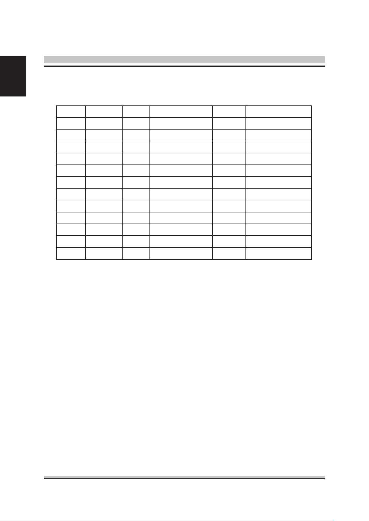
Pin GPIO Type Multiplexed with Power Connect
A2 GPIO30 I/O OC6# 3VSB 3VSB
B3 GPIO31 I/O OC7# 3VSB 3VSB
AG18 GPIO32 I/O CLKRUN# VCC3 CLKRUN#
AC19 GPIO33 I/O AZ_DOCK_EN# VCC3 PRES2
U2 GPIO34 I/O AZ_DOCK_RST# VCC3 PRES3
AD21 GPIO35 I/O SATACLKREQ# VCC3 PRES1
AH19 GPIO36 I/O SATA2GP VCC3 SATA2GP
AE19 GPIO37 I/O SATA3GP VCC3 SATA3GP
AD20 GPIO38 I/O Unmultiplexed VCC3 NC
AE20 GPIO39 I/O Unmultiplexed VCC3 NC
A14 GPIO48 I/O GNT4# VCC3 PGNT#4
AG24 GPIO49 I/O CPUPERGD VTT CPU_PWRGD
56
Page 57

5.1 Packing List
1. VBOX-3000 System
2. Power adapter
3.Mounting bracket
4. 1 GB DDRII SO-DIMM Memory (Optional)
5. 2 GB DDRII SO-DIMM Memory (Optional)
6. 2.5" 160GB Hard Disk Drive (Optional)
7. 802.11 b/g/n WiFi Kit (Optional)
8. 8GB MLC Type SSD (Optional)
9. 16GB MLC Type SSD (Optional)
English
10. 8GB SLC Type SSD (Optional)
11. 16GB SLC Type SSD (Optional)
12. VESA Mounting Kit (Optional)
57
 Loading...