


SH79F085/SH79F165 Application Note
SH79F085/SH79F165 Application Note
1 Introduction
SH79F085/SH79F165 is an 8051 compatible micro-controller with a redesigned CPU of high efficiency and high
performance. The device provides high-endurance Flash program memory to store user’s code. In circuit programming
and debugging is offered to facilitate testing and debugging the systems using SH79F085/SH79F165 without removing the
circuit from the board.
The Sinowealth 8051 JET51 Driver is intended to provide the product development engineer with a complete
microcontroller design tool set for Sinowealth 8 bit microcontrollers. Software control of the JET51 Driver is advanced by
the Keil µ vision Integrated Development Environment via a JTAG interface, which allows editing, building, downloading
and source debugging from a single environment.
1.1 Package
SH79F165: SOP24/SOP28 package
SH79F085: TSSOP20 package
2 Using Target Board
2.1 Software Installation
Steps
1) Install Keil c uvision2 (V2.34 or above) or uvision3。
2)
Install JET51_Keil_Vxxx.exe (Vxxx means version), the device library for Sinowealth 8-bit microcontrollers, to the
Keil C directory.
Connect the JET51emluator to the PC via a USB cable. The red power LED and green USB LED will turn on if the
3)
installation is successful.
2.2 Target Board
Set up the target board as follows:
1) Connect the flat cable from the SH79F085/SH79F165 target board to the JET51emluator via JTAG
2) Connect C pin with external 47uF capacitor to GND.
3) The JTAG pins of the SH79F085/SH79F165 cannot be used as I/O function when downloading and debugging .
To communicate successfully with the emulator, make sure the JTAG pins are connected with no loads.
1/27
V 1.0

SH79F085/SH79F165 Application Note
4) Make sure the selected options (Oscillator option, Power option, etc) on the Setting dialog are the same as what
target board actually selects.
5) The capacitance between VDD and GND cannot be greater than 220µF; otherwise communication error may
occur.
S
H
7
9
F
0
8
5
/
S
H
7
9
F
1
6
5
USB
PWR
USB
JET51
VDD
GND
GND
TCK
TDI
TMS
TDO
GND
10
PINs
10
PINs
VDD
TCK
TDI
TMS
TDO
GND
Target Board
When designing user’s own board, 5 jumpers connecting JTAG pins with application circuit are recommended. To
program the device or run the device in emulation mode, the jumpers should be disconnected.
SH79F085/
SH79F165
VDD
TCK
TDI
TMS
TDO
GND
JET 51
To Application
Circuit
Jumper
2/27
V 1.0

SH79F085/SH79F165 Application Note
2.3 Creating a Project
The following steps describe how to create a new project.
Note: The source file – aa.asm located in ...\user directory.
3/27
V 1.0

SH79F085/SH79F165 Application Note
An empty project has been created, then setting the attribute as follow.
4/27
V 1.0

SH79F085/SH79F165 Application Note
The attribute of project is now finished, and then the program will be added to the project as follow.
5/27
V 1.0

SH79F085/SH79F165 Application Note
p
Step12:
步骤 12:将鼠标移至程序开
Right click the blank space at the
始处,按鼠标右键,选择头文
program file star, which a pop-up menu
comes up. Select the head file of menu
件, 头文件自动加入程序
item, and add head file to program.
中。
Right click the head file to open a
头文件加入后, 将鼠标移至头
pop-up menu. Select the menu
文件处,按鼠标右键,可以打开
item ”Open document <SH79F165.H>”
头文件。
to o
en the head file in a new window.
6/27
V 1.0

SH79F085/SH79F165 Application Note
2.4 Building a Project and Downloading to the Flash Memory
2.4.1 Building a Project
Select Project->Build target or click the corresponding button to build the source files. If no compilation error
and linking error are found, OBJ and HEX files will generate. The generated files can be found in the directory
\user.
7/27
V 1.0
SH79F085/SH79F165 Application Note
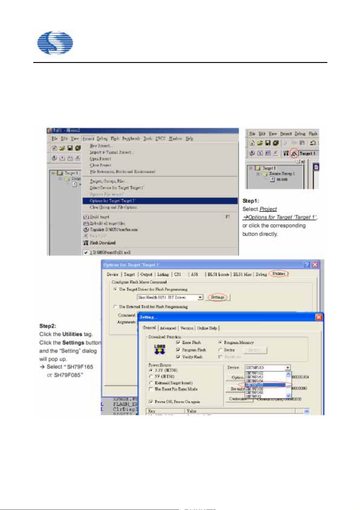
2.4.2 Downloading to the Flash Program Memory
2.4.2.1 Setting for Downloading
Before downloading the code, some options, including programming device, device’s code option and power supply
source, must be determined. Since the options will save automatically each time you set them, this step can be skipped
once you did before.
8/27
V 1.0

SH79F085/SH79F165 Application Note
9/27
V 1.0

SH79F085/SH79F165 Application Note
Note: Two ways are available to power up the target board, which can be determined by Step3.
1) Type 1: Power supply from JET51
Please select “3.3V (JET51)” or “5V (JET51)” for power source option. Check Power Off, Power On again option, which
means that each time the Download or Debug button has been clicked, JET51 will power off the target board before it
powers up the target board again. Use this way if debugging code is in process or downloading error is found.
In this case, the JET51 driver powers up the target board when downloading and debugging the program. Since the power
is used from JET51 driver, any external voltage should not be applied to the target board. Type 1 is recommended if the
current consumption of the target board is less than 20mA.
2) Type 2: Power supply from your own external voltage.
Select “External (Target board)” for power source option. In this case, an external voltage should be applied to the target
board. Please strictly follow the steps below to power on successfully.
Step1: Power off the target board
Step2: Connect JET51emluator with the target board
Step3: Connect the USB cable from JET51emluator to PC. The red power LED and green USB LED will turn on if the
connection is successful.
Step4: Apply external voltage to the target board.
Once the target board has been set up as previously described, you can download and debug the application program
repeatedly without powering off and reconnecting the target board again
2.4.2.2 Downloading to the Flash Memory
10/27
V 1.0

SH79F085/SH79F165 Application Note
2.5 Debugging Source Code
Select the menu item Debug->Start/Stop Debug Session or click the corresponding button to enter the debugging mode of
the device. Once the device enters into its debugging mode, a yellow arrow will point to 0000H location and the SP register
in left pane read 07H. the feature of in circuit debugging enable the designer to develop and debug source code by setting
breakpoints, single stepping and watching variables, and CPU status and peripheral registers. Running at full speed
enable testing hardware and applications in read time.
Note:
1) The instruction at the breakpoint location has been executed when the device breaks.
2) The next statement of ACALL or LCALL statement will execute when step over command executes.
3) The emluator supports total 7 breakpoints. If more than 7 breakpoints have been set, the last 7 breakpoints work and
the others are ignored.
4) power off the device and disconnect it from JET51 driver.
5) To run the device in normal mode, Apply external voltage to the target board again, and the device will operate under
11/27
V 1.0

SH79F085/SH79F165 Application Note
3 Design Tips
3.1 CPU
The SH79F085/SH79F165 is an 8051 compatible microcontroller with an enhanced CPU core. The CPU function is
intensified in the following aspects:
3.1.1 The SH79F085/SH79F165 CPU machine cycle is the same as its oscillator clock, while the traditional 8051 CPU
machine cycle is composed of 12 oscillator clock cycles. When the same oscillator frequency is selected, the
SH79F085/SH79F165 devices run almost 10 times faster than the traditional 8051 devices. See the SH79F085/
SH79F165 datasheet for the detail instruction execution cycles.
3.1.2 The SH79F085/SH79F165 has implemented enhanced multiplication and division instructions, where 16bit×8bit
and16bit÷8bit operations are supported by introducing an AUXC register. Set the MUL and DIV bits of the INSCON
register to perform the 16bit operation. Please clear these two bits when the 16bit operation is terminated.
3.1.3 The SH79F085/SH79F165 has implemented dual data pointers (DPTR and DPTR1). It is convenient for the user to
branch table and move data using two data pointers. Configure the DPS bit the INSCON register to select the
corresponding data pointer. Please clear the DPS bit when the DPTR1 operation is complete.
3.1.4 The SH79F085/SH79F165 provides XPAGE to represent the high byte address of RAM and only with indirect
instruction MOVX @Ri, A or MOVX A, @Ri to access external RAM above 256 bytes. it is recommended to clear
XPAGE when operation is complete.
3.1.5 The SH79F085/SH79F165 resets when a required low pulse is applied on the RESET pin, while the traditional
8051 devices require a high pulse to reset.
3.1.6 The SH79F085/SH79F165 can distinguish whether to access FLASH ROM or to access information EEPROM
block by FAC bit. It is recommended to clear FAC bite when operation is complete.
3.1.7 The SH79F085/SH79F165 provides SFR addressed 80H~FFH with page control bits BKS1, BKS0. It is
recommended to clear these two bits when page operation is complete.
For more detail description please refers to the DATASHEET.
3.2 FLASH Program Memory
3.2.1
The SH79F165 contains 16K bytes Flash program memory organized in 16 sectors of 1024 bytes, The SH79F085
contains 8K bytes Flash program memory organized in 8 sectors of 1024 bytes, Every two sectors can be encrypted.
When the security bits are not set, each sector could be erased by the user’s code in the other sectors. Mass erase
operation could erase all the sectors including the last sector (by Flash programmer only).
3.2.2 The Flash program memory also could be used as EEPROM. Flash memory could be programmed and erased by
the user’s code (SSP mode). The bits of the Flash memory could be programmed from 0 to 1 directly, but when to be
programmed from 1 to 0, the Flash memory should do Sector Erase. The program time for 1 byte FLASH ROM is related
with system clock. but will not longer than 50us for programming 1 byte and will not longer than 30ms for erasing 1 sector.
3.2.3 Using a Flash programmer, in circuit programming (ICP) operation could be used to download application code
without removing the device from the user’s application circuit board. Note that capacitance loads should not be
12/27
V 1.0

SH79F085/SH79F165 Application Note
connected to the JTAG pins, and the capacitance between VDD and GND should not be more than 220µF;
otherwise the downloading operation may be fail.
3.2.4 Programming the Flash Memory in SSP Mode
3.2.4.1 The following steps describe how to program Flash memory bytes:
1) Clear the global interrupt enable bit. Although all pending interrupts would be ignored during programming
operation, the interrupt flag bits would also be set. If an interrupt flag were set during programming operation, the
execution would branch to the interrupt service routine when the programming operation is completed and the
interrupt is enabled again.
2) Clearing FAC bit as 0 if operation location is at program block;
Setting FAC bit as 1 if operation location is at information block or EEPROM like block.
3) Write the XPAGE, IB_OFFSET registers. These two registers denote the programming location, where the
IB_OFFSET register maps to the lower address of the byte to be programmed and the XPAGE register
corresponds to the higher address of the byte to be programmed.
4) Write the IB_DATA register. The data of this register will be programmed to the specified byte of the Flash memory.
5) Configure the IB_CON1~IB_CON5 registers consecutively. Write these registers the following values:
IB_CON1Æ #6EH ; 6EH denotes programming operation
IB_CON2Æ #05H
IB_CON3Æ #0AH
IB_CON4Æ #09H
IB_CON5Æ #06H
Note: Load the registers with the above values in the exact order above. Once the programming operation is completed,
these five registers will be cleared automatically to avoid undesired programming. Reload these five registers to start
another programming operation.
Write the IB_CON5 register to initiate the programming action, which makes the device enter IDLE mode. The
6)
device will be waked up automatically when the programming operation is done. This step is taken automatically
by hardware without user’s assistance.
4 NOP instructions follow, which ensures CPU to wake up from IDLE mode correctly and stably when
7)
programming process is finished.
8) Go to step3 for the next programming operation, if necessary.
9) Clear the XPAGE register. Set the global interrupt enable bit if needed. Set FAC bit as 1 or 0 if needed.
10) Sample:
CLR EA ;Step1
ORL FLASHCON,#01H ; Step2, Writing EEPROM like block
MOV XPAGE,#00H ; Step3
MOV IB_OFFSET,#00H
MOV IB_DATA,#05H ; Step4
MOV IB_CON1,#6EH ; Step5
MOV IB_CON2,#05H
MOV IB_CON3,#0AH
MOV IB_CON4,#09H
MOV IB_CON5,#06H ; Step6
NOP ; Step7
13/27
V 1.0

SH79F085/SH79F165 Application Note
NOP
NOP
NOP
MOV XPAGE,#00H ; Step8
ANL FLASHCON,#0FEH ; Step9
SETB EA
Note: Replace the data with your when developing your own application.
3.2.4.2 Erasing the Flash Memory in SSP Mode
Perform the erase operation as follows
1) Clear the global interrupt enable bit. Although all pending interrupts would be ignored during programming
operation, the interrupt flag bits would also be set. If an interrupt flag were set during programming operation, the
execution would branch to the interrupt service routine when the programming operation is completed and the
interrupt is enabled again.
2) Clearing FAC bit as 0 if operation location is at program block.
Setting FAC bit as 1 if operation location is at information block or EEPROM like block.
3) Load the XPAGE register with appropriate sector number which wanted to erase, The SH79F165 contains 16K
bytes Flash program memory organized in 16 sectors of 1024 bytes. The Bit7 to bit6 in the XPAGE register is
reserved. Bit5 to bit2 denote the erasing sector number. The SH79F085 contains 8K bytes Flash program memory
organized in 8 sectors of 1024 bytes. The Bit7 to bit5 in the XPAGE register is reserved. Bit4 to bit2 denote the
erasing sector number. Bit1~bit0 have no effect on the operation. The IB_OFFSET register is not used in this
situation.
4) Configure the IB_CON1~IB_CON5 registers with the following values:
IB_CON1----Æ #0E6H ; 0E6H denotes erasing operation
IB_CON2 ---Æ #05H
IB_CON3----Æ #0AH
IB_CON4 ----Æ #09H
IB_CON5 ----Æ #06H
Note: Load the registers with the above values in the exact order above. Once the erasing operation is complete,
these five registers will be cleared automatically to avoid undesired erasure. Reload these five registers to start
another erasing operation.
5) Write the IB_CON5 register to initiate the erasing action, which makes the device enter IDLE mode. The device
will be waked up automatically when the erasing process terminates. This step is completed by hardware without
software assistance.
6) 4 NOP instructions follow, which ensures CPU to wake up from IDLE mode correctly and stably when
programming process is finished.
7) Go to step3 for the next erasing operation, if necessary.
8) Clear the XPAGE register. Set the global interrupt enable bit if needed.
Set FAC bit as 1 or 0 if needed.
14/27
V 1.0

SH79F085/SH79F165 Application Note
9) Sample:
CLR EA ; Step1
ORL FLASHCON,#01H ; Step2, Erase EEPROM sector
MOV XPAGE,#00H ; Step3
MOV IB_CON1,#0E6H ; Step4
MOV IB_CON2,#05H
MOV IB_CON3,#0AH
MOV IB_CON4,#09H
MOV IB_CON5,#06H
NOP ; Step6
NOP
NOP
NOP
MOV XPAGE,#00H ; Step7
ANL FLASHCON,#0FEH ; Step8
SETB EA
3.3 RAM
3.3.1 SH79F085/SH79F165 provides 256 bytes internal RAM and 256 bytes external RAM.
3.3.2 The Internal RAM addressed from 00H~FFH can be accessed by direct instructions or indirect instructions.
The internal RAM addressed from 80H~FFH only can be accessed by indirect instructions, and the SFR location will
be accessed by direct instruction.
3.3.3 The external RAM is addressed from 00H~FFH. User can access external RAM from 00H~FFH with MOVX A, @Ri
instruction
3.4 System Clock and Oscillator
The SH79F085/SH79F165 oscillator clock from one of the five oscillator types (32.768kHz crystal, crystal oscillator,
ceramic oscillator, Internal 128kHz RC or Internal 16.6M RC)
3.4.1 The SH79F085/SH79F165 is two clocks for system at the same time. The two Clocks contain low frequency
oscillator and high frequency oscillator. Low frequency oscillator is selected as system clock prescaler when power
on. If select high frequency oscillator is use as system clock prescaler input (OSCSCLK), need set corresponding
register.
3.4.2 The system clock changed from low-frequency (Internal 128kHz RC or 32.768kHz crystal) to high-frequency
(Internal 16.6MHz RC or crystal/ceramic oscillator), the steps below must be done in sequence:
Step1: Set HFON=1, turn on high frequency oscillator;
Step2: Wait at least 2ms; (note)
Step3: Set FS=1, select high frequency oscillator as OSCSCLK.
Note: Different types of high-frequency oscillator need wait for different start-up time.
Internal 16.6MHz RC: about 30us;
High-frequency crystal oscillator: about 2ms + 213T
High-frequency ceramic oscillator: about 100us + 29T
15/27
OSC
OSC
V 1.0

SH79F085/SH79F165 Application Note
3.4.3 The system clock changed from high-frequency (Internal 16.6MHz RC or crystal/ceramic oscillator) to
low-frequency (Internal 128kHz RC or 32.768kHz crystal), Refer to following step:
Step1: Clearing FS bit, select low frequency oscillator as OSCSCLK;
Step2: Delay one NOP instruction;
Step3: Clearing HFON bit, turn off high-frequency oscillator.
3.4.4 When system power on, CLKS[1:0]=11, The default is 1/12 of system clock prescaler (If code option
OP_OSC=1010, External 32.768kHz crystal is not effect as system clock prescaler. This means that prescaler is invalid).
3.4.5 When code option OP_OSC is 1010, the 32.768kHz oscillator speed up control bit (32K_SPDUP) is set by
hardware automatically in all kinds of RESET such as Power on reset, watch dog reset etc. to speed up the
32.768kHz oscillator, shorten the 32.768kHz oscillator start-oscillating time. And this bit also can be set or cleared
by software if necessary. Such as set before entering Power-Down mode and cleared when Power-Down mode
wake up. It should be noticed that turning off 32.768kHz oscillator speed up (clear this bit) could reduce the system
power consumption.
3.5 Idle & Power-down
Three NOP instructions after the power-managed instruction are required to allow the CPU to prepare for execution when
leaving IDLE mode or Power-down mode. An example is shown below for your reference.
MOV 8EH, #55H
ORL PCON,#01H ;idle mode (or #02H: Power-down mode)
NOP ; Three NOP instructions are required
NOP ;
NOP ;
…… ; Breakpoint should be set after the third NOP instructions when watching
; wake up of IDLE mode or Power-down mode.
Note:To reduce the start up time of oscillator, set the 32K_SPDUP bit in the CLKCON register by software before entering
Power-down.
3.6 External Interrupt
3.6.1
When the I/O pin is used as the external interrupt input, only the pin configured as input can cause the interrupt to
occur. Turn on the internal pull-up resistors by software. The pull-up resistance is about 30 kΩ. When the I/O pin outputs
low just before it is configured as the external interrupt input and low-level trigger is selected at the same time, an interrupt
request would happen in respect that a low level, remaining on the pin for the capacitance loads and slow internal pulling
up, was detected by the built-in low level detecting circuitry. After turning on the internal pull-up resistor, a delay, for
example 5 NOP instructions, is recommended to eliminate the undetermined state before enabling the interrupt.
3.6.2 Before switching from the external interrupt input to a second function of the I/O pin, clear the EXx (x=0~2) bits to
turn off the external interrupts, or the execution would vector to the external interrupt service routine if the requirements of
the interrupt is met for changing the port function.
3.6.3 The following steps illustrate how to configure an I/O pin to an external interrupt input (INT0/P1.4 is taken for
example):
16/27
V 1.0

SH79F085/SH79F165 Application Note
1) Clear the POCR.4 bit to select input mode, and set the P0PCR.4 bit to turn on the internal pull up resistor.
2) 5 NOP instructions
3) Configure the IT0 bit of the TCON register to select the trigger mode, and clear the IE0 bit to remove the possible
generated interrupt flag.
4) Set the EX0 bit in the IEN0 register to enable the external interrupt 0, and set the EA bit to enable the global interrupt.
3.6.4 Follow the steps below to wake up IDLE and Power-down mode correctly (INT0/P1.4 is taken for example):
1) Configure the P1.4 pin as described above. Once, according to the selected trigger mode, the CPU detected a falling
edge or a low level, it will exit from IDLE and Power-Down mode.
2) The execution would resume from the interrupt service routine of the external interrupt 0 immediately after the
waking-up of the CPU. Return to the main program by RETI instruction.
3) The instructions after the 3 NOP instructions will execute later.
3.7 ADC&PGA
3.7.1 The SH79F085/SH79F165 includes a full-differential 20-bit Σ-∆ analog to digital converter. The ADC module can
work in IDLE mode and the ADC interrupt will wake up the IDLE mode if interrupt is enabled. The module is
disabled in Power-Down mode. But user can wake up in Power-Down with timer3 interrupt.
3.7.2 The SH79F085/SH79F165 built-in regulator of 2.7V for ADC module. Before using the ADC module must set
REGEN bit in REGCON register to enable regulator. This regulator maximum output current is 15mA, enough used
in sensors of electronic scales. VDDR pin is regulator output port of 2.7V. Recommended to be connected 47 uF
electrolytic capacitor and 104 ceramic capacitor to AGND.
3.7.3 The GND pin is digital power ground. The AGND pin is analog power ground. So PCB layout need connect GND to
AGND.
3.7.4 The ADC module pins may be shared as I/O function, Corresponding input channels will be selected when set
CH[2:0] bits in ADCH register. The VREF pin is use as ADC reference voltage function port when setting P27OS bit
in ADCH register.
3.7.5 The VREF pin is use as reference voltage whether internal or external function. This pin can’t be used as I/O port
and connect a 104 capacitor to AGND.
3.7.6 VIN+/VIN- pins are PGA positive/negative output port. A 104 capacitor must be connected between VIN+ and VIN-
in order to enhance the anti-noise performance of ADC. This port can’t use as O/I when The ADC module is
enabled.
3.7.7 AIN+/AIN- pins are differential analog positive/negative input port. Both ports are input front-end of PGA. Therefore,
it can be calculated by input-output relationship: (AINx+/-)*Gain=VIN+/- .
3.7.8 Common-input voltage range of AIN+/AIN- pins is 0.4V~2.0V. To improve the ADC’s effective accuracy,
recommended that user adopt common-input voltage of about 1.35V at analog input port.
3.7.9 To improve the anti-noise performance of system, In PCB layout, digital and analog power supply traces should be
separated and not overlapping, digital ground and analog ground adopt single-point connection. Analog ground should be
17/27
V 1.0

SH79F085/SH79F165 Application Note
large area coated with copper, making noise and interference source in the shortest path back to the input source of power.
If it is double-sided PCB board, analog ground should not be many via hole. The spacing of hole generally is 1cm~2cm.
3.7.10 To improve the anti-noise performance of system, recommended that the bead or resistor of 1000Ω should be
connected of series each differential input channel, then connect a 104 capacitor between positive and negative. In
PCB layout, line of trace width generally is more 20 mil and parallel trace. Analog device must close chip pin of mcu
such as sensor, resistors and capacitors. Refer to following application circuit schematic.
3.7.11 To improve the anti-noise performance of system, recommended that power supply of sensor connects to T-type
filter and filter must close chip pin. Refer to following application circuit schematic.
3.7.12 The SH79F085/SH79F165 provides a low noise programmable gain amplifier. This PGA provides amplification
setting of 12.5, 25, 50, 75, 100, 125, 150 and 200 for ADC analog input. The actual gain of PGA will possible lower
of 3%~7%, but doesn’t affect application. A chopper function is included, which can be use for eliminate offset of
PGA. Work clock of 1kHz is recommended. Chopper must be enabled when PGA is enabled. Otherwise accuracy
of ADC should be affected.
18/27
V 1.0

SH79F085/SH79F165 Application Note
3.7.13 Application Circuit Schematic:
JP1
JTAG
VDD
1
TCK
2
TDI
3
TMS
4
TDO
5
6
JTAG Interface
VDD
JP2
5V
2
1
POWER
U1
1
FLT/P0.2
2
T3/P0.3
3
BUZ/P1.0
4
TDO/RXD/P1.1
5
TMS /TXD/P1.2
6
RST/P0.4
7
XTAL1/T0/P0.5
8
XTAL2/T1/P0.6
9
TDI/T2/P1.3
10
TCK/T2EX/INT0/P1.4
11
AIN1+/INT1/P1.5
12
AIN1-/IN T2/P1.6
13
P1.7
14
P2.0
SH79F165
P0.1/PWMN
P0.0/PWMP
P2.7/V REF
P2.6/AIN0-
P2.5/AIN0+
P2.4/VIN-
P2.3/V IN+
P2.2/AIN2-
P2.1/AIN2+
J2
0
J1
1
2
3
4
Sensor
GND
VDD
VDDR
AGND
AGND
28
27
26
25
C
24
23
22
21
20
19
18
17
16
15
AIN+
AIN-
Analog Circuit
R21KR3
C1
47uF/16V
104
C4
C6
104
1K
C7
104
AGND
VDDR
C5
104
AGND
R1
10
R4
10
C2
104
C8
47uF/16V
VDDR
VDD
C3
104
Note: in application circuit, the R2 and R3 is the bead to improve the effect which will be better than the resistor
19/27
V 1.0

SH79F085/SH79F165 Application Note
3.7.14 Example:(the ADC conversion data send PC with UART)
#include"SH79F165.H"
ORG 0000H
LJMP START
ORG 0033H
LJMP ADC_IRQ
ORG 0100H
START:
;SYSCLK from low-frequency to high-frequency
MOV CLKCON,#08H
CALL DELAY_2ms ;Delay 2ms
MOV CLKCON,#0CH
;ADC Module Initialization
MOV REGCON, #01H ;2.7V output
MOV ADCON, #02H ;AIN2
MOV ADT, #0ADH ;ADC Sample Freq = 25Hz
MOV ADCH, #0EFH ; Internal REF=0.8V
MOV PGAM, #0C4H ;PGA Gain=100,CHOP=1K
ORL ADCON, #80H ;ADC Enable
;Timer1/UART Initialization
MOV SCON, #40H
MOV TCON, #00H
MOV TCON1, #0CH
MOV TMOD, #21H
MOV TL1, #0caH
MOV TH1, #0caH ;Baud Rate=9600Hz
SETB TR1 ;Enable Timer1
ADC_WAIT:
MOV A,ADCON
NOP
JNB ACC.6, ADC_WAIT ;Wait for AD Conversion
ANL ADCON, #0BFH ;Clear ADCIF Flag
MOV R0,ADDL
MOV R1,ADDM
MOV R2,ADDH
MOV SBUF,#0A3H
JNB TI,$
CLR TI
MOV SBUF,R0
JNB TI,$
CLR TI
MOV SBUF,R1
JNB TI,$
CLR TI
MOV SBUF,R2
JNB TI,$
CLR TI
LJMP ADC_WAIT
20/27
V 1.0

SH79F085/SH79F165 Application Note
3.8 Watch Dog Timer
3.8.1 The SH79F085/SH79F165 builds in a watchdog timer (WDT). The WDT time-out period is from 1ms to 4 seconds.
A WDT reset will occur if WDT is time out. WDT reset will set the WDOF bit in the RSTSTAT register. To prevent
WDT from overflowing, access (read or write) the WDT register RSTSTAT at a given period according to the
time-out period.
3.8.2 The WDT consumes 1-2uA current during operation. If the WDT is still enabled in the Power-down mode by
OPTION, the WDT will reset CPU to leave the Power-down mode.
3.8.3 The WDT can be enabled or disabled by the code option OP_WDT permanently (See section 2.4.2.1 step3).
3.9 UART
3.9.1 The TXD/RXD pin may be shared as I/O function, the RXD pin will be configured as input-pull up automatically
when REN bit is set as 1. But the TXD pin is used as UART function only when users write data to SBUF register,
and goes back to I/O function automatically when UART transmission is over. So it is recommend to configure the
TXD pin as output high level before UART transmission which can avoid that the receiver get error information.
3.9.2 Both Timer1 and Timer2 can be selected as baud rate clock source of UART controlled by TCLK and RCLK bits.
If set TCLK or RCLK bit as logic 0, Timer1 acts as the baud rate clock source, if set TCLK or RCLK bit as logic 1,
Timer2 acts as the baud rate clock source. This shows that UART can use deferent baud rate in transmission and
reception.
3.9.3 The maximum tolerance of UART reception baud rate is ±4%.
3.10 PWM
3.10.1 The SH79F165 has one PWM module, which can provide two complementary outputs. The output polarity that is
if high active or low active is controlled by PWMS bit, each output has independent control bit, note that it is
complementary output with dead time control if the two outputs are all active, regardless polarity setting.
3.10.2
3.10.3
PWM provides interrupt function on every period overflow.
PWM has 12-bit control register, when writing PWMPH/L, PWMDH/L registers, low byte first, then high byte to
update the whole registers. The internal register value can’t be changed if only writing low byte.
3.10.4 PWM dead time register only can be set when PWMEN bit is 0 (that is PWM block disable), and make sure that
any time when PWM is disabled, before enable PWM again, dead time register must be clear to 0 at first, and
then set to proper value.
3.10.5 Set PWMLO register to 0x55 before writing the PWM registers, otherwise the PWM registers can’t be changed.
21/27
V 1.0

SH79F085/SH79F165 Application Note
3.11 Timer3
3.11.1 Timer 3 is a 16-bit auto-reload timer. When writing to TH3 and TL3, they are used as timer load register. When
reading from TH3 and TL3, they are used as timer counter register.
3.11.2 Read or write operation to TH3 and TL3 should follow these steps.
Write operation: Low nibble first, High nibble to update the counter.
Read operation: High nibble first, Low nibble followed.
3.11.3 Timer 3 can operate even in Power-Down mode. System clock must be high-frequency oscillator before timer3
entering Power-Down mode, and timer3 clock source must select low frequency oscillator, such as 32.768kHz
crystal and internal 128kHz RC. That is T3CLKS[1:0]=10.
3.11.4 Timer3 control and reload/counter register is placed to Bank1. When user operate timer, need set BKS0 bit in
INSCON register. But clear BKS0 is as 0 after operating complete.
3.11.5 Example:(Timer3 wake up in Power-Down mode)
#include"SH79F165.H"
ORG 0000H
LJMP START
ORG 005BH
LJMP Timer3_IRQ
ORG 0100H
START:
;SYSCLK from low-frequency to high-frequency
MOV CLKCON,#08H
CALL DELAY_2ms ;Delay 2ms
MOV CLKCON,#0CH
;Set timer3 Register
MOV INSCON,#40H ; Bank1
MOV T3CON,#02H
MOV TL3,#080H
MOV TH3,#0FFH
SETB TR3
MOV INSCON,#00H ; Bank0
MOV IEN1,#10H ;Enable Timer3 Interrupt
SETB EA
PD_Mode:
;Entering Power-Down mode
MOV SUSLO,#55H
ORL PCON,#02H
NOP
NOP
NOP
SJMP PD_Mode
Timer3_IRQ: ;Timer3 Interrupt Subroutine
NOP
RETI
22/27
V 1.0

SH79F085/SH79F165 Application Note
3.12 Application Circuit
3.12.1 Electronic Weighing Scale
- VIN+/VIN-/VREF as ADC pin
- SH79F085 built-in digital circuit regulator. It can output stable voltage of 1.8V for core and peripherals.
- SH79F085 built-in analog circuit regulator. It can output stable voltage of 2.7V for analog devices.
- SH79F085 built-in measure voltage of V
sample point. If SCH[2:0]≠100
,
This resistor will be disconnected.
channel, an internal 80kΩ resistor will connect VDD with GND to provide
DD
Battery
SENSOR
GND
VDDR
AGND
VDD
0
47uF
3.0V~5.5V
GND
AGND
104
51K
10K
51K
104
104
47uF
47uF
104
VDD
GND
VDD
GND
C
VDDR
AGND
VREF
VIN+
VIN-
AIN2-
AIN2+
AIN0+
AIN0-
SH79F085
P0.4
P0.5
P0.6
P0.6
P1.1
P1.2
P1.3
P1.4
P1.5
P1.6
P1.7
P2.0
P1.0
CS
SDA
SCK
LED/LCD
DRIVER
VDD
GND
1K
GND
23/27
V 1.0

SH79F085/SH79F165 Application Note
3.12.2 Industry Temperature Controller
- VIN+/VIN-/VREF as ADC pin
- SH79F165 built-in digital circuit regulator. It can output stable voltage of 1.8V for core and peripherals.
- SH79F165 built-in analog circuit regulator. It can output stable voltage of 2.7V for analog devices.
- SH79F165 built-in measure voltage of V
sample point. If SCH[2:0]≠100
,
This resistor will be disconnected.
channel, an internal 80kΩ resistor will connect VDD with GND to provide
DD
Input Voltage
0.6V
AGND
LM7805
GND
GND
REF2.5V
AGND
104
Thermistor
47u
0
AGND
Thermocouple
PT100
REF2.5V
5.0V
47uF
47uF
REF0.8V
REF2.5V
REF2.5V
104
104
104
AGND
VDD
GND
C
VDDR
AGND
VIN+
VIN-
VREF
AIN0+
AIN0-
AIN1+
AIN1-
AIN2+
AIN2-
SH79F165
P0.4
P0.5
P0.6
P0.5
P0.6
P1.4
P1.7
PWMP
RXD
TXD
P1.0
P0.1
P0.2
P0.3
P2.0
CS
SDA
SCK
T2
set
up
down
enter
LED/LCD
DRIVER
GND
RS485
Interface
VDD
VDD
Frequency Input
PWM output
DC12V
GND
DC12V
OUT12
OUT11
OUT1
OUT22
OUT21
OUT2
AGND
Input Voltage
Input Voltage
ADR431
GND
LM7812
GND
47uF
100u
24/27
104
DC12V
REF2.5V
GND
104
REF0.8V
VDD
VDD
GND
DC12V
GND
DC12V
GND
OUT32
OUT31
OUT3
OUT42
OUT41
OUT4
V 1.0

SH79F085/SH79F165 Application Note
Appendix1:
Target Board Circuit Schematic
MCU_VD D
RESET
MCU OSC
J1
DC12V
U2 7805
3
2
1
100uF/25V
R3
10k
K1
RESET
1
C2
C1
104
J3
2
1
D3
VDD
1N4001
J2
2
1
GND
C5
103
C6
12pF
Y1
16M
C7
12pF
3
Vin
Vout
GND
C3
2
104
R1
470
D1
1N4001
VDD
D2
1N4001
C4
47uF/16V
JP1
MCU_VDD
2
R2
1
470
IDD_TEST
Power
D4
S1
RESET
S2
XTAL1
S3
XTAL2
MCU_VD D
J7
1
2
AIN0
VDD
J4
1 2
3 4
5 6
7 8
9 10
JTAG
JTAG
1
P02
2
P03
3
P10
4
P11
5
P12
6
P04
7
P05
8
AIN2+
AIN2-
AIN1+
AIN1-
P06
9
P13
10
P14
11
AIN1+
12
AIN1-
13
P17
14
P20
VDDR
R19
R20
0
0
C11
104
AGND
VDDR
R14
50K
J8
R16
10K
AIN1
C13
104
R18
15K
AGND
P04
P05
P06
R13
50K
AIN0+
R15
C12
10K
104
AIN0-
R17
15K
Sensor Input
TDI
TMS
TDO
U1
FLT/P 0. 2
T3/P0.3
BUZ/ P1. 0
TDO/RXD/P1.1
TMS/TXD/P1.2
RST/P 0. 4
XTAL1/T0/P 0.5
XTAL2/T1/P 0.6
TDI/T2/P1 .3
TCK/T2EX/INT0/P1.4
AIN1+/ INT1/P1 .5
AIN1-/INT2/P1.6
P1.7
P2.0
SH79F165
J6
1
2
3
4
AIN2
1
2
3
4
P14TCK
P13
P12
P11
MCU_VDD
C8
104
P0.1/PWMN
P0.0/PWMP
VDDR
AGND
P2.7/VREF
P2.6/AIN0-
P2.5/AIN0+
P2.4/VIN-
P2.3/VIN+
P2.2/AIN2-
P2.1/AIN2+
C9
GND
C
VDD
104
100uF/16V
VDDR
C16
AGND
28
27
26
25
24
23
22
21
20
19
18
17
16
15
R4
R5
R6
R7
R12
MCU_VDD
0
0
0
0
0
VREF
AIN0AIN0+
VINVIN+
AIN2AIN2+
AGND
I/O PORT
P01
P00
C
C14
104
C10
104
VIN+
P23
VINP24
AIN0+
P25
AIN0P26
VREF
P27
FLT/P 0. 2
T3/P0.3
BUZ/ P1. 0
TDO/RXD/P1.1
TMS/TXD/P1.2
RST/P 0. 4
VDDR
XTAL1/T0/P0.5
AGND
XTAL2/T1/P0.6
TDI/T2/P1 .3
TCK/T2EX/INT0/P1.4
AIN1+/INT1/P 1.5
AIN1-/INT2/P1.6
P1.7
P2.0
C
VREF
VIN+
VIN-
AIN1+
P15
AIN1P16
AIN2+
P21
AIN2P22
C15
47uF/16V
R21
0
AGND
R8
0
R9
0
R10
0
R11
0
P02
P03
P10
P11
P12
P13
P14
P15
P16
P17
P20
J5
1 2
3 4
5 6
7 8
9 10
11 12
13 14
15 16
17 18
19 20
21 22
23 24
25 26
27 28
PORT
MCU_VDD
P01
P00
C
VDD
VDDR
AGND
P27
P26
P25
P24
P23
P22
P21
P0.1/PWMN
P0.0/PWMP
GND
C
VDDR
AGND
P2.7/VREF
P2.6/AIN0P2.5/AIN0+
P2.4/VINP2.3/VIN+
P2.2/AIN2P2.1/AIN2+
25/27
V 1.0

SH79F085/SH79F165 Application Note
Appendix2:
Target Board
A target board is provides to help user to familiar with the SH79F085/SH79F165.
SH79F165 Target Board (SOP28)
Function blocks on the board
A. Power LED
B. Pin Reset Key
C. Emulator Interface (JTAG Interface)
The emulator interface communicates with the JET51emluator via a 10-pin cable. The power supply can also be
provided from VDD pin of the emulator interface when the JET51 emulator is connected to PC.
D. Power Supply Interface1 (VDD/GND)
The power supply interface1 supplies the power of SH79F085/SH79F165, where the user determines the voltage
level.
E. Power Supply Interface2
The Power supply interface2 is a DC power jack (Outer to GND Inner to 9~12V). A fixed voltage (5V), regulated by
U2 components, will be applied to the device.
Note: The power source of target board can be selected among power supply interface 1, power supply interface 2 and
emulator interface. Whichever option is chosen, the applied voltage can be measured through power supply interface 1.
F. Current test interface.
26/27
V 1.0

SH79F085/SH79F165 Application Note
4. Revision History
version Content Date
1.0
original
Jul. 2011
27/27
V 1.0
 Loading...