

Page 1
Obsolete - Not Recommended for New Designs
Features Description
UL635H256
Low Voltage PowerStore 32K x 8 nvSRAM
• High-performance CMOS non-
volatile static RAM 32768 x 8 bits
• 35 and 45 ns Access Times
• 15 and 20 ns Output Enable
Access Times
• I
= 8 mA typ. at 200 ns Cycle
CC
Time
• Automatic STORE to EEPROM
on Power Down using system
capacitance
• Software initiated STORE
• Automatic STORE Timing
6
• 10
STORE cycles to EEPROM
• 100 years data retention in
EEPROM
• Automatic RECALL on Power Up
• Software RECALL Initiation
• Unlimited RECALL cycles from
EEPROM
• Wide voltage range: 2.7 ... 3.6 V
(3.0 ... 3.6 V for 35 ns type)
• Operating temperature range:
0 to 70 °C
-40 to 85 °C
• QS 9000 Quality Standard
• ESD protection > 2000 V
(MIL STD 883C M3015.7-HBM)
• RoHS compliance and Pb- free
• Package:SOP28 (330 mil)
The UL635H256 has two separate
modes of operation: SRAM mode
and nonvolatile mode. In SRAM
mode, the memory operates as an
ordinary static RAM. In nonvolatile
operation, data is transferred in
parallel from SRAM to EEPROM or
from EEPROM to SRAM. In this
mode SRAM functions are disabled.
The UL635H256 is a fast static
RAM (35 and 45 ns), with a nonvolatile electrically erasable PROM
(EEPROM) element incorporated
in each static memory cell. The
SRAM can be read and written an
unlimited number of times, while
independent nonvolatile data resides in EEPROM. Data transfers
from the SRAM to the EEPROM
(the STORE operation) take place
automatically upon power down
using charge stored in system
capacitance. Transfers from the
EEPROM to the SRAM (the
RECALL operation) take place
automatically on powerup.
The UL635H256 combines the
high performance and ease of use
of a fast SRAM with nonvolatile
data integrity.
STORE cycles also may be initiated under user control via a software sequence.
Once a STORE cycle is initiated,
further input or output are disabled
until the cycle is completed.
Because a sequence of addresses
is used for STORE initiation, it is
important that no other read or
write accesses intervene in the
sequence or the sequence will be
aborted.
RECALL cycles may also be initiated by a software sequence.
Internally, RECALL is a two step
procedure. First, the SRAM data is
cleared and second, the nonvolatile information is transferred into
the SRAM cells.
The RECALL operation in no way
alters the data in the EEPROM
cells. The nonvolatile data can be
recalled an unlimited number of
times.
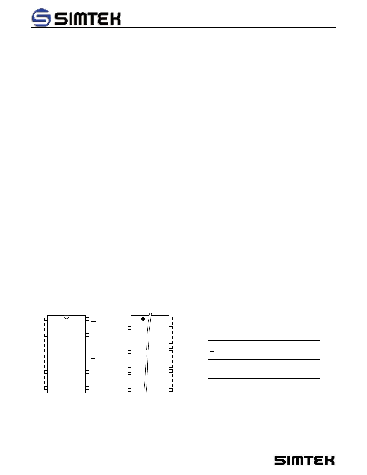
Pin Configuration
A14
1
A12
2
A7
3
A6
4
A5
5
A4
6
A3
7
A2
A1
A0
DQ0
DQ1
DQ2
VSS
SOP
8
9
10
11
12
13
14
Top View
March 31, 2006
VCC
28
W
27
A13
26
A8
25
A9
24
A11
23
G
22
A10
21
E
20
DQ7
19
DQ6
18
DQ5
17
DQ4
16
DQ3
15
STK Control #ML0059
n. c.
VCC
n. c.
A11
A9
A8
A13
W
A14
A12
A7
A6
A5
A4
A3
Pin Description
G
1
2
3
4
5
6
7
8
TSOP
9
10
11
12
13
14
15
16
Top View
32
31
30
29
28
27
26
25
24
23
22
21
20
19
18
17
n.c.
A10
E
DQ7
DQ6
DQ5
DQ4
DQ3
VSS
DQ2
DQ1
DQ0
A0
A1
A2
n.c.
1
Signal Name Signal Description
A0 - A14 Address Inputs
DQ0 - DQ7 Data In/Out
E
G
W
Chip Enable
Output Enable
Write Enable
VCC Power Supply Voltage
VSS Ground
Rev 1.0
Page 2
UL635H256
Block Diagram
A5
A6
A7
A8
A9
A11
A12
A13
A14
DQ0
DQ1
DQ2
DQ3
DQ4
DQ5
DQ6
DQ7
Tr uth Table for SRAM Operations
SRAM
Array
512 Rows x
Row Decoder
Input Buffers
64 x 8 Columns
Column I/O
Column Decoder
A0 A1 A2 A3 A4 A10
EEPROM Array
512 x (64 x 8)
STORE
RECALL
Power
Control
Store/
Recall
Control
Software
Detect
V
CC
V
SS
V
CC
A0 - A13
G
E
W
Operating Mode E W G DQ0 - DQ7
Standby/not selected H
**
Internal Read L H H High-Z
Read L H L Data Outputs Low-Z
Write L L
*
Data Inputs High-Z
* H or L
Characteristics
All voltages are referenced to VSS = 0 V (ground).
All characteristics are valid in the power supply voltage range and in the operating temperature range specified.
Dynamic measurements are based on a rise and fall time of ≤ 5 ns, measured between 10 % and 90 % of V
input levels of V
with the exception of the t
Absolute Maximum Ratings
Power Supply Voltage V
Input Voltage V
Output Voltage V
Power Dissipation P
= 0 V and VIH = 3 V. The timing reference level of all input and output signals is 1.5 V,
IL
-times and ten-times, in which cases transition is measured ± 200 mV from steady-state voltage.
dis
a
Symbol Min. Max. Unit
CC
I
O
D
-0.5 4.6 V
-0.3 VCC+0.5 V
-0.3 VCC+0.5 V
, as well as
I
High-Z
1W
Operating Temperature C-Type
K-Type
Storage Temperature T
a: Stresses greater than those listed under „Absolute Maximum Ratings“ may cause permanent damage to the device. This is a stress
rating only, and functional operation of the device at condition above those indicated in the operational sections of this specification is
not implied. Exposure to absolute maximum rating conditions for extended periods may affect reliability.
STK Control #ML0059
T
a
stg
2
0
-40
70
85
°C
°C
-65 150 °C
Rev 1.0
March 31, 2006
Page 3
UL635H256
Recommended
Operating Conditions
Power Supply Voltage V
Input Low Voltage V
Input High Voltage V
Symbol Conditions Min. Max. Unit
t
CC
= 35 ns
c
t
= 45 ns
c
-2 V at Pulse Width
IL
IH
10 ns permitted
DC Characteristics Symbol Conditions
Operating Supply Current
Average Supply Current during
STORE
Operating Supply Current
at tcR = 200 ns
(Cycling CMOS Input Levels)
Average Supply Current during
PowerStore Cycle
Standby Supply Current
(Cycling TTL Input Levels)
b
c
b
c
d
I
CC1
I
CC2
I
CC3
I
CC4
I
CC(SB)1
V
V
V
t
t
V
E
W
V
V
V
W
V
V
V
V
V
V
E
CC
IL
IH
c
c
CC
= 3.6 V
= 0.8 V
= 2.2 V
= 35 ns
= 45 ns
= 3.6 V
≤ 0.2 V
≥ V
-0.2 V
CC
IL
IH
CC
IL
IH
CC
IL
IH
CC
≤ 0.2 V
≥ V
CC
= 3.6 V
≥ V
CC
≤ 0.2 V
≥ V
CC
= V
CCmin
= 0.2 V
≥ V
CC
= 3.6 V
= V
IH
-0.2 V
-0.2 V
-0.2 V
-0.2 V
3.0
2.7
3.6
3.6
-0.3 0.8 V
2.2 VCC+0.3 V
C-Type K-Type
Min. Max. Min. Max.
45
35
47
37
34mA
10 11 mA
22mA
V
V
Unit
mA
mA
Standby Supply Curent
d
(Stable CMOS Input Levels)
b: I
and I
CC1
The current I
and I
c: I
CC2
d: Bringing E
table. The current I
March 31, 2006
are depedent on output loading and cycle rate. The specified values are obtained with outputs unloaded.
CC3
is measured for WRITE/READ - ratio of 1/2.
CC1
are the average currents required for the duration of the respective STORE cycles.
CC4
≥ VIH will not produce standby current levels until any nonvolatile cycle in progress has timed out. See MODE SELECTION
CC(SB)1
STK Control #ML0059
t
c
t
c
I
CC(SB)
V
CC
E
V
IL
V
IH
is measured for WRITE/READ - ratio of 1/2.
3
= 35 ns
= 45 ns
= 3.6 V
≥ V
CC
≤ 0.2 V
≥ V
CC
-0.2 V
-0.2 V
Rev 1.0
11
9
12
10
mA
mA
11mA
Page 4
UL635H256
DC Characteristics Symbol Conditions
C-Type K-Type
Unit
Min. Max. Min. Max.
Output High Voltage
Output Low Voltage
Output High Current
Output Low Current
Input Leakage Current
Output Leakage Current
High at Three-State- Output
Low at Three-State- Output
SRAM Memory Operations
Switching Characteristics
No.
Read Cycle
High
Low
V
V
I
OH
I
OL
I
I
I
OHZ
I
OLZ
OH
OL
IH
IL
V
I
I
V
V
V
V
V
V
V
V
V
CC
OH
OL
CC
OH
OL
CC
IH
IL
CC
OH
OL
= V
CC
min
=-2 mA
2.4
= 2 mA
= V
CC
min
= 2.4 V
= 0.4 V 2
= 3.6 V
= 3.6 V
= 0 V -1
= 3.6 V
= 3.6 V
= 0 V -1
2.4
0.4
-2
2
1
-1
1
-1
Symbol 35 45
Alt. IEC Min.Max.Min.Max.
0.4
-2 mA
mA
1 μA
μA
1 μA
μA
Unit
V
V
1 Read Cycle Time
2 Address Access Time to Data Valid
f
g
3 Chip Enable Access Time to Data Valid t
4 Output Enable Access Time to Data
Valid
HIGH to Output in High-Z
5E
6G
HIGH to Output in High-Z
h
h
7E LOW to Output in Low-Z t
LOW to Output in Low-Z t
8G
9 Output Hold Time after Address Change t
10 Chip Enable to Power Active
11 Chip Disable to Power Standby
e: Parameter guaranteed but not tested.
f: Device is continuously selected with E
g: Address valid prior to or coincident with E
h: Measured ± 200 mV from steady state output voltage.
e
d, e
and G both Low.
transition LOW.
t
AVAV
t
AVQ V
ELQV
t
GLQV
t
EHQZ
t
GHQZ
ELQX
GLQX
AXQX
t
ELICCH
t
EHICCL
t
cR
t
a(A)
t
a(E)
t
a(G)
t
dis(E)
t
dis(G)
t
en(E)
t
en(G)
t
v(A)
t
PU
t
PD
35 45 ns
35 45 ns
35 45 ns
15 20 ns
13 15 ns
13 15 ns
55ns
00ns
33ns
00ns
35 45 ns
STK Control #ML0059
4
Rev 1.0
March 31, 2006
Page 5
UL635H256
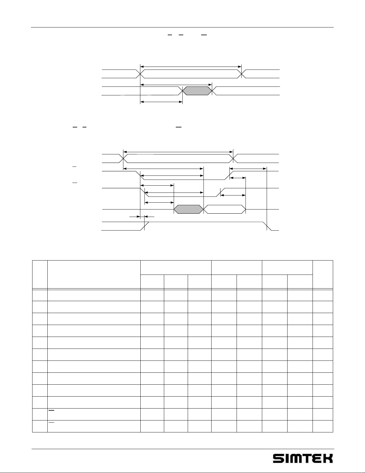
Read Cycle 1: Ai-controlled (during Read cycle: E = G = VIL, W = VIH)
t
(1)
cR
Ai
DQi
Output
Previous Data Valid
t
v(A)
Read Cycle 2: G-, E-controlled (during Read cycle: W = VIH)
Ai
E
t
t
en(G)
t
PU
en(E)
(10)
G
DQi
DQi
Output
Output
I
CC
High Impedance
ACTIVE
STANDBY
Address Valid
t
(2)
a(A)
(9)
t
(1)
cR
Address Valid
t
(2)
a(A)
t
(3)
a(E)
(7)
t
a(G)
(8)
g
(4)
Output Data Valid
f
Output Data Valid
t
(11)
PD
t
dis(E)
(5)
t
(6)
dis(G)
Switching Characteristics
No.
Write Cycle
12 Write Cycle Time t
13 Write Pulse Width t
Alt. #1 Alt. #2 IEC
AVAV
WLWH
14 Write Pulse Width Setup Time t
15 Address Setup Time t
16 Address Valid to End of Write t
17 Chip Enable Setup Time t
AVW L
AVW H
ELWH
18 Chip Enable to End of Write t
19 Data Setup Time to End of Write t
20 Data Hold Time after End of Write t
21 Address Hold after End of Write t
22 W
LOW to Output in High-Z
h, i
23 W HIGH to Output in Low-Z t
DVWHtDVEH
WHDXtEHDX
WHAXtEHAX
t
WLQZ
WHQX
Symbol 35 45
t
AVAV
WLEH
t
AVEL
t
AVEH
ELEH
t
cW
t
w(W)
t
su(W)
t
su(A)
t
su(A-WH)
t
su(E)
t
w(E)
t
su(D)
t
h(D)
t
h(A)
t
dis(W)
t
en(W)
Min. Max.
35 45 ns
25 30 ns
25 30 ns
00ns
25 30 ns
25 30 ns
25 30 ns
12 15 ns
00ns
00ns
13 15 ns
55ns
Min. Max.
Unit
March 31, 2006
STK Control #ML0059
5
Rev 1.0
Page 6

UL635H256
Write Cycle #1: W-controlled
Ai
E
W
DQi
Input
DQi
Output
Write Cycle #2: E-controlled
j
t
su(A)
(15)
Previous Data Valid
j
Address Valid
t
su(E)
t
su(A-WH)
t
w(W)
t
dis(W)
t
cW
(12)
(17)
(16)
(13)
t
(19)
su(D)
Input Data Valid
(22)
High Impedance
t
h(D)
t
en(W)
t
h(A)
(21)
(20)
(23)
Ai
E
W
DQi
Input
DQi
Output
undefined
t
(15)
su(A)
L- to H-level
t
cW
Address Valid
t
(18)
w(E)
t
(14)
su(W)
(12)
t
(19)
su(D)
Input Data Valid
High Impedance
t
h(A)
t
h(D)
(21)
(20)
H- to L-level
i: If W is low and when E goes low, the outputs remain in the high impedance state.
or W must be VIH during address transition.
j: E
STK Control #ML0059
6
Rev 1.0
March 31, 2006
Page 7

Nonvolatile Memory Operations
Mode Selection
UL635H256
E
W
A13 - A0
(hex)
Mode I/O Power Notes
H X X Not Selected Output High Z Standby
L H X Read SRAM Output Data Active m
L L X Write SRAM Input Data Active
LH 0E38
31C7
03E0
3C1F
303F
0FC0
LH 0E38
31C7
03E0
3C1F
303F
0C63
k: The six consecutive addresses must be in order listed. W must be high during all six consecutive cycles. See STORE cycle and RECALL
cycle tables and diagrams for further details.
The following six-address sequence is used for testing purposes and should not be used: 0E38, 31C7, 03E0, 3C1F, 303F, 339C.
l: While there are 15 addresses on the UL635H256, only the lower 14 are used to control software modes.
Activation of nonvolatile cycles does not depend on the state of G
m: I/O state assumes that G
≤ VIL.
Read SRAM
Read SRAM
Read SRAM
Read SRAM
Read SRAM
Nonvolatile STORE
Read SRAM
Read SRAM
Read SRAM
Read SRAM
Read SRAM
Nonvolatile RECALL
.
Output Data
Output Data
Output Data
Output Data
Output Data
Output High Z
Output Data
Output Data
Output Data
Output Data
Output Data
Output High Z
Active k, l
k, l
k, l
k, l
k, l
k, l
Active k, l
k, l
k, l
k, l
k, l
k, l
PowerStore
No.
Power Up RECALL
24 Power Up RECALL Duration
25 STORE Cycle Duration
Time allowed to Complete SRAM
26
Cycle
f
f, e
Low Voltage Trigger Level V
n: t
March 31, 2006
starts from the time VCC rises above V
RESTORE
STK Control #ML0059
Symbol
Conditions Min. Max. Unit
Alt. IEC
n
t
RESTORE
650 μs
the power supply decay
t
PDSTORE
rate has to be smaller
than 10 Vs
-1
after the
10 ms
start of the STORE
operation
SWITCH
t
DELAY
SWITCH
.
7
Rev 1.0
500 ns
2.4 2.7 V
Page 8

UL635H256
PowerStore and automatic Power Up RECALL
V
CC
3.0 V
V
SWITCH
t
PowerStore
Power Up
RECALL
W
(24)
t
RESTOR
E
DQi
POWER UP
RECALL
Software Controlled STORE/RECALL
No.
Cycle
k, o
27 STORE/RECALL Initiation Time t
28 Chip Enable to Output Inactive
29 STORE Cycle Time
30 RECALL Cycle Time
q
r
31 Address Setup to Chip Enable
32 Chip Enable Pulse Width
33 Chip Disable to Address Change
p
s
s, t
s
t
PDSTORE
BROWN OUT
NO STORE
(NO SRAM WRITES)
Symbol
Alt. IEC
AVAV
t
ELQZ
t
ELQXS
t
ELQXR
t
AVELN
t
ELEHN
t
EHAXN
t
cR
t
dis(E)SR
t
d(E)S
t
d(E)R
t
su(A)SR
t
w(E)SR
t
h(A)SR
p
(24)
t
RESTORE
p
t
DELAY
BROWN OUT
PowerStore
35
45
Unit
Min. Max.
Min. Max.
35 45 ns
600 600 ns
10 10 ms
20 20 μs
00ns
25 30 ns
00ns
o: The software sequence is clocked with E controlled READs.
p: Once the software controlled STORE or RECALL cycle is initiated, it completes automatically, ignoring all inputs.
q: Note that STORE cycles (but not RECALL) are aborted by V
r: An automatic RECALL also takes place at power up, starting when V
s: Noise on the E
t: If the Chip Enable Pulse Width is less than t
once it has been exceeded for the RECALL to function properly.
V
SWITCH
the end of the low pulse, however the STORE or RECALL will still be initiated.
pin may trigger multiple READ cycles from the same address and abort the address sequence.
(see Read Cycle) but greater than or equal t
a(E)
STK Control #ML0059
< V
CC
(STORE inhibit).
SWITCH
exceeds V
CC
8
SWITCH
and takes t
, than the data may not be valid at
w(E)SR
Rev 1.0
. VCC must not drop below
RESTORE
March 31, 2006
Page 9

UL635H256
Software Controlled STORE/RECALL Cycle
t
(27)
cR
Ai
E
DQi
Output
t
su(A)SR
High Impedance
ADDRESS 1
t
w(E)SR
(32)
(31)
VAL ID
Software Controlled STORE/RECALL Cycle
t
(29)
cR
Ai
E
DQi
Output
t
su(A)SR
High Impedance
ADDRESS 1
t
w(E)SR
(33)
(34)
VAL ID
t, u, v
(E = HIGH after STORE initiation)
t
(27)
cR
ADDRESS 6
t
h(A)SR
(33)
t
d(E)S
VAL ID
t
dis(E)SR
t, u, v, w
(E = LOW after STORE initiation)
ADDRESS 6
t
h(A)SR
(35)
t
su(A)SR
(33)
t
d(E)S
t
dis(E)SR
t
(29)
(31) (32)
(28)
t
h(A)SR
d(E)R
t
d(E)R
(30)
VAL ID
(30)
(35)
u: W must be HIGH when E is LOW during the address sequence in order to initiate a nonvolatile cycle. G may be either HIGH or LOW
throughout. Addresses 1 through 6 are found in the mode selection table. Address 6 determines wheter the UL635H256 performs a STORE
or RECALL.
must be used to clock in the address sequence for the Software controlled STORE and RECALL cycles.
v: E
March 31, 2006
STK Control #ML0059
9
Rev 1.0
Page 10

UL635H256
Test Configuration for Functional Check
w: In measurement of t
x: Between V
Capacitance
and VSS must be connected a high frequency bypass capacitor 0.1 μF to avoid disturbances.
CC
e
Input Capacitance
Output Capacitance
A0
A1
A2
A3
A4
A5
V
IH
V
IL
Input level according to the
relevant test measurement
-times and ten-times the capacitance is 5 pF.
dis
A6
A7
A8
A9
A10
A11
A12
A13
A14
E
W
G
Conditions Symbol Min. Max. Unit
V
CC
V
I
f
T
a
= 3.0 V
= V
SS
= 1 MHz
= 25 °C
Simultaneous measure-
ment of all 8 output pins
3 V
1.1 k
950
V
O
w
30 pF
8pF
7pF
X
V
CC
DQ0
DQ1
DQ2
DQ3
DQ4
DQ5
DQ6
DQ7
V
SS
C
I
C
O
All Pins not under test must be connected with ground by capacitors.
Ordering Code
Example
G1S2 45CUL635H256
Type
Package
S = SOP28 (330mil) Type 1
S2 = SOP28 (330mil) Type 2
Operating Temperature Range
C = 0 to 70 °C
K = -40 to 85 °C
y: on special request
Device Marking (example)
Product specification
ZMD
UL635H256S2C
45 Z 0425
G1
Leadfree Option
blank = Standard Package
G1 = Leadfree Green Package
Access Time
35 = 35 ns
45 = 45 ns (V
(VCC = 3.0 ... 3.6 V)
= 2.7 ... 3.6 V)
CC
Date of manufacture
(The first 2 digits indicating
the year, and the last 2
digits the calendar week.)
Internal Code
STK Control #ML0059
10
Rev 1.0
Leadfree Green Package
March 31, 2006
Page 11

UL635H256
Device Operation
The UL635H256 has two separate modes of operation:
SRAM mode and nonvolatile mode. The memory operates in SRAM mode as a standard fast static RAM.
Data is transferred in nonvolatile mode from SRAM to
EEPROM (the STORE operation) or from EEPROM to
SRAM (the RECALL operation). In this mode SRAM
functions are disabled.
STORE cycles may be initiated under user control via a
software sequence and are also automatically initiated
when the power supply voltage level of the chip falls
below V
. RECALL operations are automatically
SWITCH
initiated upon power up and may also occur when the
V
rises above V
CC
, after a low power condition.
SWITCH
RECALL cycles may also be initiated by a software
sequence.
SRAM READ
The UL635H256 performs a READ cycle whenever E
and G are LOW and W is HIGH. The address specified
on pins A0 - A14 determines which of the 32768 data
bytes will be accessed. When the READ is initiated by
an address transition, the outputs will be valid after a
delay of t
puts will be valid at t
. If the READ is initiated by E or G, the out-
cR
a(E)
or at t
, whichever is later.
a(G)
The data outputs will repeatedly respond to address
changes within the t
access time without the need for
cR
transition on any control input pins, and will remain
valid until another address change or until E
brought HIGH or W
is brought LOW.
or G is
SRAM WRITE
A WRITE cycle is performed whenever E
and W are
LOW. The address inputs must be stable prior to
entering the WRITE cycle and must remain stable until
either E
or W goes HIGH at the end of the cycle. The
data on pins DQ0 - 7 will be written into the memory if it
is valid t
t
before the end of an E controlled WRITE.
su(D)
It is recommended that G
before the end of a W controlled WRITE or
su(D)
is kept HIGH during the
entire WRITE cycle to avoid data bus contention on the
common I/O lines. If G
turn off the output buffers t
is left LOW, internal circuitry will
after W goes LOW.
dis (W)
Automatic STORE
The UL635H256 uses the intrinsic system capacitance
to perform an automatic STORE on power down. As
long as the decay rate from the system power supply is
smaller than 15 Vs
-1
the UL635H256 will safely and
automatically STORE the SRAM data in EEPROM on
power down.
In order to prevent unneeded STORE operations, automatic STORE will be ignored unless at least one
WRITE operation has taken place since the most
recent STORE or RECALL cycle. Software initiated
STORE cycles are performed regardless of whether or
not a WRITE operation has taken place.
Automatic RECALL
During power up, an automatic RECALL takes place. At
a low power condition (power supply voltage < V
SWITCH
an internal RECALL request may be latched. As soon
as power supply voltage exceeds the sense voltage of
V
be initiated and will take t
, a requested RECALL cycle will automatically
SWITCH
RESTORE
to complete.
If the UL635H256 is in a WRITE state at the end of
power up RECALL, the SRAM data will be corrupted.
To help avoid this situation, a 10 kΩ resistor should be
connected between W
and power supply voltage.
Software Nonvolatile STORE
The UL635H256 software controlled STORE cycle is
initiated by executing sequential READ cycles from six
specific address locations. By relying on READ cycles
only, the UL635H256 implements nonvolatile operation
while remaining compatible with standard 32K x 8
SRAMs. During the STORE cycle, an erase of the previous nonvolatile data is performed first, followed by a
parallel programming of all the nonvolatile elements.
Once a STORE cycle is initiated, further inputs and outputs are disabled until the cycle is completed.
Because a sequence of addresses is used for STORE
initiation, it is important that no other READ or WRITE
accesses intervene in the sequence or the sequence
will be aborted.
To initiate the STORE cycle the following READ
sequence must be performed:
1. Read addresses 0E38 (hex) Valid READ
2. Read addresses 31C7 (hex) Valid READ
3. Read addresses 03E0 (hex) Valid READ
4. Read addresses 3C1F (hex) Valid READ
5. Read addresses 303F (hex) Valid READ
6. Read addresses 0FC0 (hex) Initiate STORE
Cycle
Once the sixth address in the sequence has been
entered, the STORE cycle will commence and the chip
will be disabled. It is important that READ cycles and
not WRITE cycles be used in the sequence, although it
is not necessary that G
valid. After the t
STORE
be LOW for the sequence to be
cycle time has been fulfilled, the
SRAM will again be activated for READ and WRITE
operation.
)
March 31, 2006
STK Control #ML0059
11
Rev 1.0
Page 12

UL635H256
Software Nonvolatile RECALL
A RECALL cycle of the EEPROM data into the SRAM
is initiated with a sequence of READ operations in a
manner similar to the STORE initiation. To initiate the
RECALL cycle the following sequence of READ operations must be performed:
1. Read addresses 0E38 (hex) Valid READ
2. Read addresses 31C7 (hex) Valid READ
3. Read addresses 03E0 (hex) Valid READ
4. Read addresses 3C1F (hex) Valid READ
5. Read addresses 303F (hex) Valid READ
6. Read addresses 0C63 (hex) Initiate RECALL
Cycle
Internally, RECALL is a two step procedure. First, the
SRAM data is cleared and second, the nonvolatile
information is transferred into the SRAM cells. After
t
cycle time the SRAM will once again be ready for
d(E)R
READ and WRITE operations.The RECALL operation
in no way alters the data in the EEPROM cells. The
nonvolatile data can be recalled an unlimited number of
times.
Hardware Protection
The UL635H256 offers hardware protection against
inadvertent STORE operation through V
When V
CC
< V
SWITCH
all software STORE operations
Sense.
CC
will be inhibited.
Low Average Active Power
The UL635H256 has been designed to draw significantly less power when E
is LOW (chip enabled) but
the cycle time is longer than 45 ns.
When E
is HIGH the chip consumes only standby current.
The overall average current drawn by the part depends
on the following items:
1. CMOS or TTL input levels
2. the time during which the chip is disabled (E
3. the cycle time for accesses (E
LOW)
HIGH)
4. the ratio of READs to WRITEs
5. the operating temperature
6. the V
CC
level
The information describes the type of component and shall not be considered as assured characteristics. Terms of
delivery and rights to change design reserved.
STK Control #ML0059
12
Rev 1.0
March 31, 2006
Page 13

UL635H256
LIFE SUPPORT POLICY
Simtek products are not designed, intended, or authorized for use as components in systems intended for surgical
implant into the body, or other applications intended to support or sustain life, or for any other application in which
the failure of the Simtek product could create a situation where personal injury or death may occur.
Components used in life-support devices or systems must be expressly authorized by Simtek for such purpose.
LIMITED WARRANTY
The information in this document has been carefully checked and is believed to be reliable. However, Simtek
makes no guarantee or warranty concerning the accuracy of said information and shall not be responsible for any
loss or damage of whatever nature resulting from the use of, or reliance upon it. The information in this document
describes the type of component and shall not be considered as assured characteristics.
Simtek does not guarantee that the use of any information contained herein will not infringe upon the patent,
trademark, copyright, mask work right or other rights of third parties, and no patent or licence is implied hereby.
This document does not in any way extent Simtek’s warranty on any product beyond that set forth in its standard
terms and conditions of sale.
Simtek reserves terms of delivery and reserves the right to make changes in the products or specifications, or
both, presented in this publication at any time and without notice.
March 31, 2006
Page 14

Change record
Date/Rev Name Change
01.11.2001 Ivonne Steffens format revision and release for „Memory CD 2002“
03.07.2002 Matthias Schniebel adding 35 ns type with V
= 3.0 ... 3.6 V
CC
25.09.2002 Matthias Schniebel Adding „Type 1“ to SOP28 (330mil)
09.01.2003 Matthias Schniebel Removing 55 ns type
20.10.2003 Matthias Schniebel Low Voltage Trigger Level V
SWITCH
= 2.4 ... 2.7 V (old: 2.5 ... 2.7 V)
changing max. decay rate from the system power supply to 15 Vs
-1
)
= 47 mA, I
CC1
CC(SB)1
= 12mA
05.12.2003 Matthias Schniebel I
(old: 10 Vs
= 8 mA typ. at 200 ns Cycle Time
CC
adding K-Type with 35 ns: I
21.04.2004 Matthias Schniebel adding „Leadfree Green Package“ to ordering information
adding „Device Marking“
7.4.2005 Stefan Günther Page1: adding RoHS compliance and Pb- free, 10
6
endurance cycles
and 100a data retention,
add also S2 package (chip pack) and ordering code
31.3.2006 Troy Meester changed to obsolete status
1.0 Simtek Assigned Simtek Document Control Number
-1
 Loading...