

STK25CA8
128K x 8
Nonvolatile Static RAM Module
FEATURES
• Nonvolatile Storage without Battery Problems
• Directly Replaces 128K x 8 Static RAM, BatteryBacked RAM or EEPROM
• 35ns and 45ns Access Times
•
STORE
on Power Down
•
RECALL
• 22mA I
• Unlimited READ, WRITE and
• 1,000,000
• 100-Year Data Retention Over Full Commercial
Temperature Range
• Commercial and Industrial Temperatures
• 32-Pin 600 mil Dual In-Line Module
to EEPROM Initiated by
to SRAM on Power Restore
at 200ns Cycle Time
CC
RECALL
STORE
Cycles to EEPROM
AutoStore
Cycles
™
AutoStore
QuantumTrap
™ nvSRAM
™ CMOS
DESCRIPTION
The Simtek STK25CA8 is a fast static RAM with a
nonvolatile, electrically erasable
incorporated in each static memory cell. The
can be read and written an unlimited number of
times, while independent nonvolatile data resides in
the
EEPROM. Data transfers from the SRAM to the
EEPROM (the
STORE
operation) can take place automatically on power down using charge stored in system capacitance. Transfers from the
SRAM (the
RECALL
operation) take place automati-
cally on restoration of power.
PROM element
SRAM
EEPROM to the
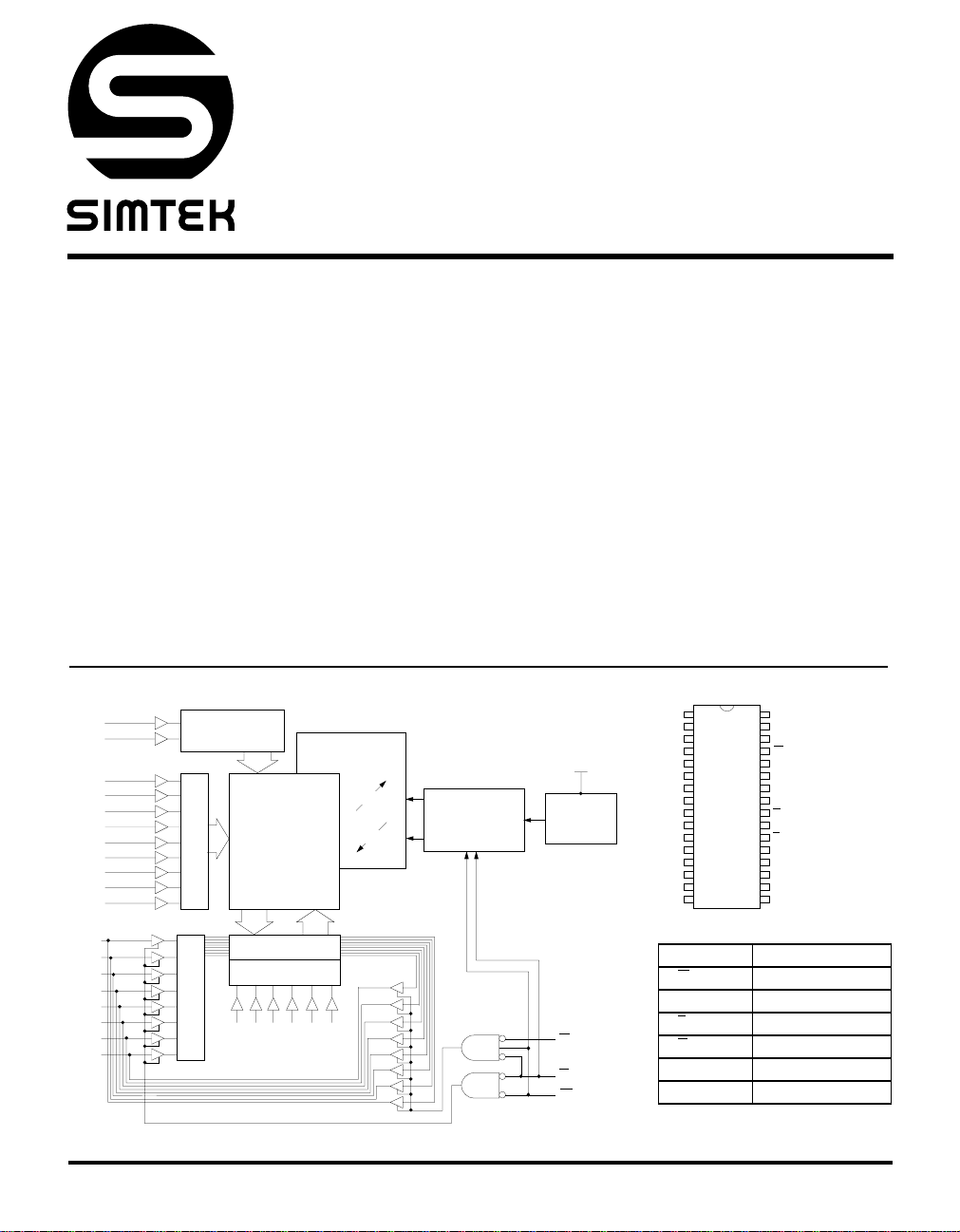
BLOCK DIAGRAM
DQ
DQ
DQ
DQ
DQ
DQ
DQ
DQ
A
15
A
16
A
5
A
6
A
7
A
8
A
9
A
11
A
12
A
13
A
14
0
1
2
3
4
5
6
7
MODULE
DECODER
STATIC RAM
ROW DECODER
COLUMN I/O
COLUMN DEC
A0A
INPUT BUFFERS
ARRAY
512 x 512
A
A
2
3
1
EEPROM ARRAY
512 x 512
512 x 512
STORE
RECALL
A
A
10
4
STORE/
RECALL
CONTROL
August 1999 6-1
V
CC
POWER
CONTROL
G
E
W
PIN CONFIGURATIONS
1
NC
2
A
16
3
A
14
4
A
12
5
A
7
6
A
6
7
A
5
8
A
4
9
A
3
10
A
2
11
A
1
12
A
0
13
DQ
0
14
DQ
1
15
DQ
2
16
V
SS
V
V
32
CC
CC
A
A
31
15
15
30
NC
NC
29
W
28
A
13
27
A
8
26
A
9
25
A
11
24
G
A
A
23
10
10
E
E
22
DQ
DQ
21
7
7
DQ
DQ
20
6
6
32 - 600 mil
19
DQ
DQ
5
5
18
DQ
DQ
Dual In-Line
4
4
DQ
DQ
17
3
3
Module
PIN NAMES
A0 - A
16
W Write Enable
DQ0 - DQ
E Chip Enable
G Output Enable
V
CC
V
SS
7
Address Inputs
Data In/Out
Power (+ 5V)
Ground
STK25CA8
ABSOLUTE MAXIMUM RATINGS
Voltage on Input Relative to VSS. . . . . . . . . . –0.6V to(VCC+ 0.5V)
Voltage on DQ
Temperature under Bias . . . . . . . . . . . . . . . . . . . . . –55°C to 125°C
Storage Temperature . . . . . . . . . . . . . . . . . . . . . . . –65°C to 150°C
Power Dissipation. . . . . . . . . . . . . . . . . . . . . . . . . . . . . . . . . . . .1W
DC Output Current (1 output at a time, 1s duration). . . . . . . .15mA
. . . . . . . . . . . . . . . . . . . . . . –0.5V to (VCC + 0.5V)
0-7
a
Note a: Stresses greater than those listed under “Absolute Maximum
Ratings” may cause permanent damage to the device. This is a
stress rating only, and functional operation of the device at conditions above those indicated in the operational sections of this
specification is not implied. Exposure to absolute maximum rating conditions for extended periods may affect reliability.
DC CHARACTERISTICS (VCC = 5.0V ± 10%)
SYMBOL PARAMETER
b
I
CC
I
CC
I
CC
I
CC
I
SB
I
ILK
I
OLK
V
V
V
V
T
Note b: I
Note c: I
Note d:
Average VCCCurrent 140
1
c
Average VCCCurrent During
2
b
Average VCC Current at t
3
c
Average VCCCurrent During
4
Cycle
d
VCCStandby Current
(Standby, Stable CMOS Input Levels)
Input Leakage Current
Off-State Output Leakage Current
Input Logic “1” Voltage 2.2 VCC+ .5 2.2 VCC + .5 V All Inputs
IH
Input Logic “0” Voltage VSS – .5 0.8 VSS – .5 0.8 V All Inputs
IL
Output Logic “1” Voltage 2.4 2.4 V I
OH
Output Logic “0” Voltage 0.4 0.4 V I
OL
Operating Temperature 0 70 –40 85 °C
A
and I
CC
CC
E ≥ VIH will not produce standby current levels until any nonvolatile cycle in progress has timed out.
are dependent on output loading and cycle rate. The specified values are obtained with outputs unloaded.
CC
1
3
and I
are the average currents required for the duration of the respective
CC
2
4
AVAV
STORE
= 200ns
AutoStore
COMMERCIAL INDUSTRIAL
MIN MAX MIN MAX
125
20 25 mA All Inputs Don’t Care, VCC = max
22 25 mA
™
18 20 mA
99mA
±2 ±2 µA
±10 ±10 µA
UNITS NOTES
150
133
STORE
mAmAt
cycles (t
AVAV
t
AVAV
W ≥ (VCC– 0.2V)
All Others Cycling, CMOS Levels
All Inputs Don’t Care
E ≥ (VCC – 0.2V)
All Others V
VCC= max
V
VCC= max
V
OUT
OUT
STORE
= 35ns
= 45ns
≤ 0.2V or ≥ (VCC – 0.2V)
IN
= VSS to V
IN
IN
CC
= VSSto VCC, E or G ≥ V
=– 4mA
= 8mA
).
IH
AC TEST CONDITIONS
Input Pulse Levels . . . . . . . . . . . . . . . . . . . . . . . . . . . . . . . 0V to 3V
Input Rise and Fall Times . . . . . . . . . . . . . . . . . . . . . . . . . . . . . . . ≤ 5ns
Input and Output Timing Reference Levels . . . . . . . . . . . . . . . 1.5V
Output Load. . . . . . . . . . . . . . . . . . . . . . . . . . . . . . . . .See Figure 1
CAPACITANCE
SYMBOL PARAMETER MAX UNITS CONDITIONS
C
IN
C
OUT
Input Capacitance
Output Capacitance
e
(TA = 25°C, f = 1.0MHz)
20 pF
28 pF
∆V = 0 to 3V
∆V = 0 to 3V
Note e: These parameters are guaranteed but not tested.
August 1999 6-2
OUTPUT
5.0V
480 Ohms
30 pF
255 Ohms
INCLUDING
SCOPE
AND FIXTURE
Figure 1: AC Output Loading
STK25CA8
SRAM READ CYCLES #1 & #2 (VCC = 5.0V ± 10%)
SYMBOLS
NO.
#1, #2 Alt. MIN MAX MIN MAX
1t
ELQV
2t
AVAV
3t
AVQV
4t
GLQV
5t
AXQX
6t
ELQX
7t
EHQZ
8t
GLQX
9t
GHQZ
10 t
ELICCH
11 t
EHICCL
t
f
ACS
t
RC
g
t
AA
t
OE
g
t
OH
t
LZ
h
t
HZ
t
OLZ
h
t
OHZ
e
t
PA
d, e
t
PS
Chip Enable Access Time 35 45 ns
Read Cycle Time 35 45 ns
Address Access Time 35 45 ns
Output Enable to Data Valid 15 20 ns
Output Hold after Address Change 5 5 ns
Chip Enable to Output Active 5 5 ns
Chip Disable to Output Inactive 13 15 ns
Output Enable to Output Active 0 0 ns
Output Disable to Output Inactive 13 15 ns
Chip Enable to Power Active 0 0 ns
Chip Disable to Power Standby 35 45 ns
PARAMETER
Note f: W must be high during SRAM READ cycles and low during SRAM WRITE cycles.
Note g: I/O state assumes
Note h: Measured
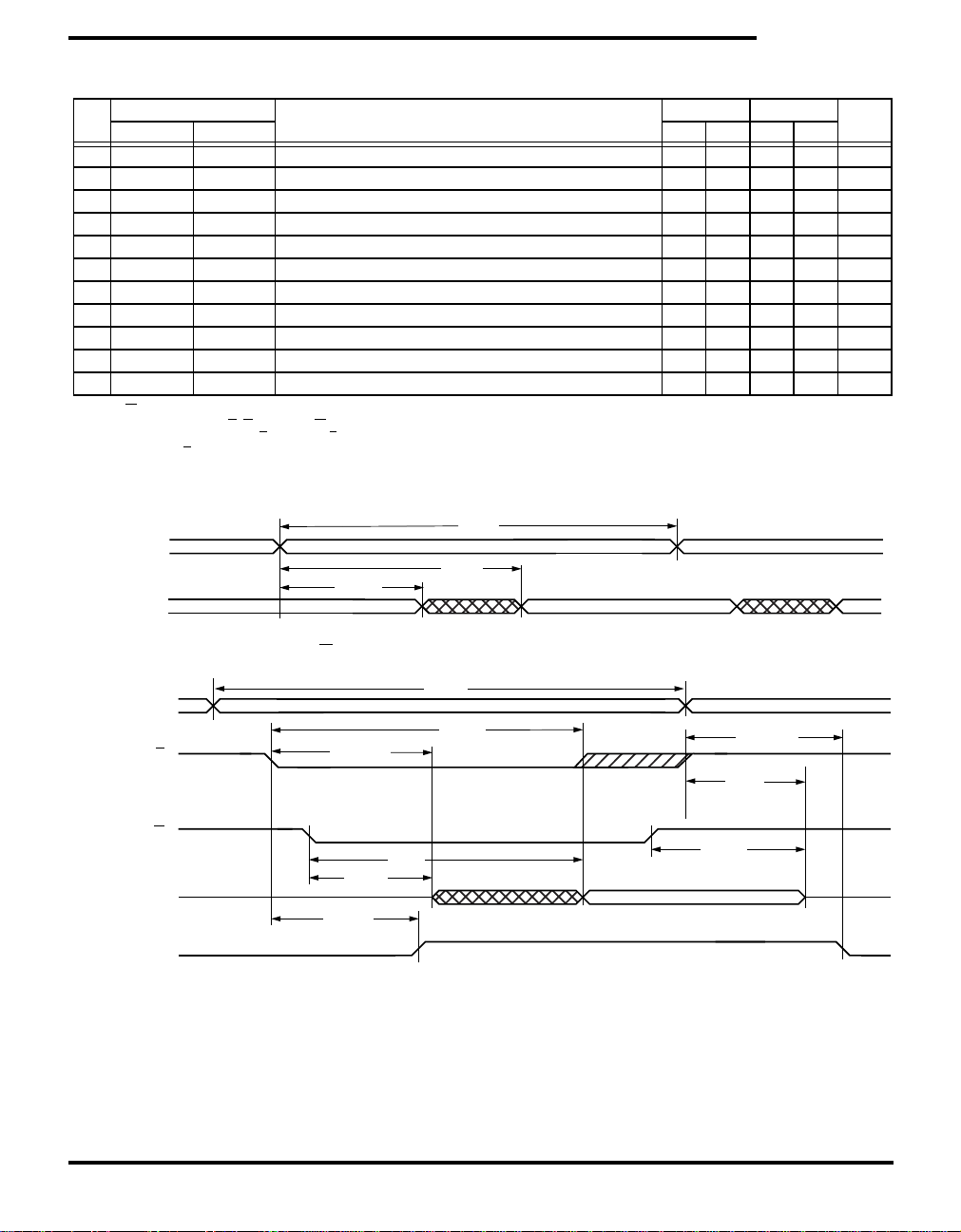
SRAM READ CYCLE #1: Address Controlled
E, G, < VIL and W > VIH; device is continuously selected.
+ 200mV from steady state output voltage.
t
AVAV
f, g
2
ADDRESS
3
t
t
AXQX
5
AVQV
DQ (DATA OUT)
DATA VALID
STK25CA8-35 STK25CA8-45
UNITS
SRAM READ CYCLE #2: E Controlled
ADDRESS
E
t
ELQX
6
f
t
AVAV
2
t
1
ELQV
G
4
t
GLQV
8
t
GLQX
DQ (DATA OUT)
10
t
ELICCH
I
CC
STANDBY
ACTIVE
August 1999 6-3
DATA VALID
t
GHQZ
11
t
EHICCL
7
t
EHQZ
9

STK25CA8
SRAM WRITE CYCLES #1 & #2 (VCC = 5.0V ± 10%)
NO.
12 t
13 t
14 t
15 t
16 t
17 t
18 t
19 t
20 t
21 t
SYMBOLS
#1 #2 Alt. MIN MAX MIN MAX
AVAV
WLWHtWLEH
ELWHtELEH
DVWHtDVEH
WHDXtEHDX
AVWHtAVEH
AVWLtAVEL
WHAXtEHAX
WLQZ
WHQX
t
h, i
AVAV
t
Write Cycle Time 35 45 ns
WC
t
Write Pulse Width 25 30 ns
WP
t
Chip Enable to End of Write 25 30 ns
CW
t
Data Set-up to End of Write 12 15 ns
DW
t
Data Hold after End of Write 0 0 ns
DH
t
Address Set-up to End of Write 25 30 ns
AW
t
Address Set-up to Start of Write 0 0 ns
AS
t
Address Hold after End of Write 0 0 ns
WR
t
Write Enable to Output Disable 13 15 ns
WZ
t
Output Active after End of Write 5 5 ns
OW
PARAMETER
Note i: If W is low when E goes low, the outputs remain in the high-impedance state.
E or W must be ≥ VIH during address transitions.
Note j:
t
ELWH
j
12
t
AVAV
14
SRAM WRITE CYCLE #1: W Controlled
ADDRESS
E
STK25CA8-35 STK25CA8-45
19
t
WHAX
UNITS
17
t
DATA IN
DATA OUT
18
t
AVWL
W
PREVIOUS DATA
t
WLQZ
AVWH
13
t
WLWH
20
SRAM WRITE CYCLE #2: E Controlled
ADDRESS
18
t
E
W
DATA IN
DATA OUT
AVEL
t
AVEH
17
j
12
t
AVAV
t
ELEH
HIGH IMPEDANCE
14
t
WLEH
13
15
t
DVWH
DATA VALID
HIGH IMPEDANCE
15
t
DVEH
DATA VALID
16
t
WHDX
19
t
EHAX
16
t
EHDX
t
WHQX
21
August 1999 6-4

STK25CA8
AutoStore
NO.
22 t
23 t
24 t
25 V
26 V
Note k: t
RESTORE
STORE
DELAY
SWITCH
RESET
RESTORE
AutoStore
25
V
SWITCH
26
V
RESET
AutoStore
POWER-UP
RECALL
™/POWER-UP
SYMBOLS
Standard MIN MAX
starts from the time VCC rises above V
™/POWER-UP
V
CC
5V
™
22
t
RESTORE
W
RECALL
PARAMETER
Power-up
RECALL
Duration 550 µsk
STORE
Cycle Duration 10 ms g
Time Allowed to Complete SRAM Cycle 1 µsg
Low Voltage Trigger Level 4.0 4.5 V
Low Voltage Reset Level 3.9 V
.
SWITCH
(VCC = 5.0V 10%)
STK25CA8
RECALL
23
t
STORE
24
t
DELAY
UNITS NOTES
DQ (DATA OUT)
POWER-UP
RECALL
BROWN OUT
NO
STORE
DUE TO
BROWN OUT
NO SRAM WRITES
NO
RECALL
(VCC DID NOT GO
BELOW V
RESET
)
(VCC DID NOT GO
BELOW V
August 1999 6-5
AutoStore
NO
RECALL
™
RESET
BROWN OUT
AutoStore
RECALL
V
CC
)
ABOVE V
™
WHEN
RETURNS
SWITCH

STK25CA8
DEVICE OPERATION
The STK25CA8 is a versatile memory module that
provides two modes of operation. The STK25CA8
can operate as a standard 128K x 8
128K x 8
EEPROM shadow to which the SRAM infor-
mation can be copied, or from which the
SRAM. It has a
SRAM can
be updated in nonvolatile mode.
NOISE CONSIDERATIONS
Note that the STK25CA8 is a high-speed memory
and so must have a high frequency bypass capacitor of approximately 0.1µF connected between V
and VSS, using leads and traces that are as short as
possible. As with all high-speed
CMOS ICs, normal
careful routing of power, ground and signals will help
prevent noise problems.
SRAM READ
The STK25CA8 performs a READ cycle whenever E
and
G are low and W is high. The address specified
on pins A
bytes will be accessed. When the
determines which of the 131,072 data
0-16
READ is initiated
by an address transition, the outputs will be valid
after a delay of t
initiated by
at t
GLQV
EorG, the outputs will be valid at t
, whichever is later (READ cycle #2). The data
(READ cycle #1). If the READ is
AVQV
ELQV
or
outputs will repeatedly respond to address changes
within the t
access time without the need for tran-
AVQV
sitions on any control input pins, and will remain valid
until another address change or until
EorGis
brought high.
SRAM WRITE
A WRITE cycle is performed whenever E and W are
low. The address inputs must be stable prior to
entering the
until either
The data on the common I/O pins DQ
ten into the memory if it is valid t
of a
W controlled WRITE or t
E controlled WRITE.
It is recommended that
entire
the common I/O lines. If
will turn off the output buffers t
WRITE cycle and must remain stable
EorW goes high at the end of the cycle.
will be writ-
0-7
before the end
DVWH
before the end of an
DVEH
G be kept high during the
WRITE cycle to avoid data bus contention on
G is left low,internal circuitry
after W goes low.
WLQZ
AutoStore
™ OPERATION
The STK25CA8 uses the intrinsic system capacitance to perform an automatic store on power down.
As long as the system power supply takes at least
t
to decay from V
STORE
down to 3.6V the
SWITCH
STK25CA8 will safely and automatically store the
SRAM data in EEPROM on power down.
In order to prevent unneeded
automatic
one
CC
recent
POWER-UP
STORE
WRITE operation has taken place since the most
STORE
or
RECALL
s will be ignored unless at least
RECALL
cycle.
STORE
During power up, or after any low-power condition
(V
CC<VRESET
latched. When V
voltage of V
be initiated and will take t
If the STK25CA8 is in a
power-up
), an internal
CC
,a
SWITCH
RECALL
, the SRAM data will be corrupted.
RECALL
request will be
once again exceeds the sense
RECALL
cycle will automatically
to complete.
RESTORE
WRITE state at the end of
To help avoid this situation, a 10K Ohm resistor
should be connected either between
V
or between E and system VCC.
CC
HARDWARE PROTECT
The STK25CA8 offers hardware protection against
inadvertent
ing low-voltage conditions. When V
externally initiated
WRITEs are inhibited.
STORE
operation and SRAM WRITEs dur-
STORE
operations and SRAM
CAP<VSWITCH
LOW AVERAGE ACTIVE POWER
The STK25CA8 draws significantly less current
when it is cycled at times longer than 50ns. If the
chip enable duty cycle is less than 100%, only
standby current is drawn when the chip is disabled.
The overall average current drawn by the
STK25CA8 depends on the following items:
1)
CMOS vs. TTL input levels; 2) the duty cycle of
chip enable; 3) the overall cycle rate for accesses;
4) the ratio of
temperature; 6) the V
READstoWRITEs; 5) the operating
level; and 7) I/O loading.
CC
operations,
W and system
, all
August 1999 6-6

ORDERING INFORMATION
STK25CA8
STK25CA8
- D 45 I
Temperature Range
Blank = Commercial (0 to 70˚C)
I = Industrial (–40 to 85˚C
)
Access Time
35 = 35ns
45 = 45ns
Package
D = 32-pin 600 mil Dual In-Line Module
August 1999 6-7

 Loading...