

SIMTEK STK20C04-W45, STK20C04-W45I, STK20C04-W35I, STK20C04-W30I, STK20C04-W35 Datasheet
...
STK20C04
STK20C04
CMOS nvSRAM
High Performance
512 x 8 Nonvolatile Static RAM
FEATURES
• 30, 35 and 45ns Access Times
• 15, 20 and 25ns Output Enable Access
• Unlimited Read and Write to
• Hardware
• Automatic
5
• 10
STORE
STORE
STORE
Initiation
Timing
cycles to EEPROM
SRAM
• 10 year data retention in EEPROM
• Automatic
• Hardware
• Unlimited
RECALL
RECALL
RECALL
on Power Up
Initiation
cycles from EEPROM
• Single 5V±10% Operation
• Commercial and Industrial Temperatures
• Available in 600 mil PDIP package
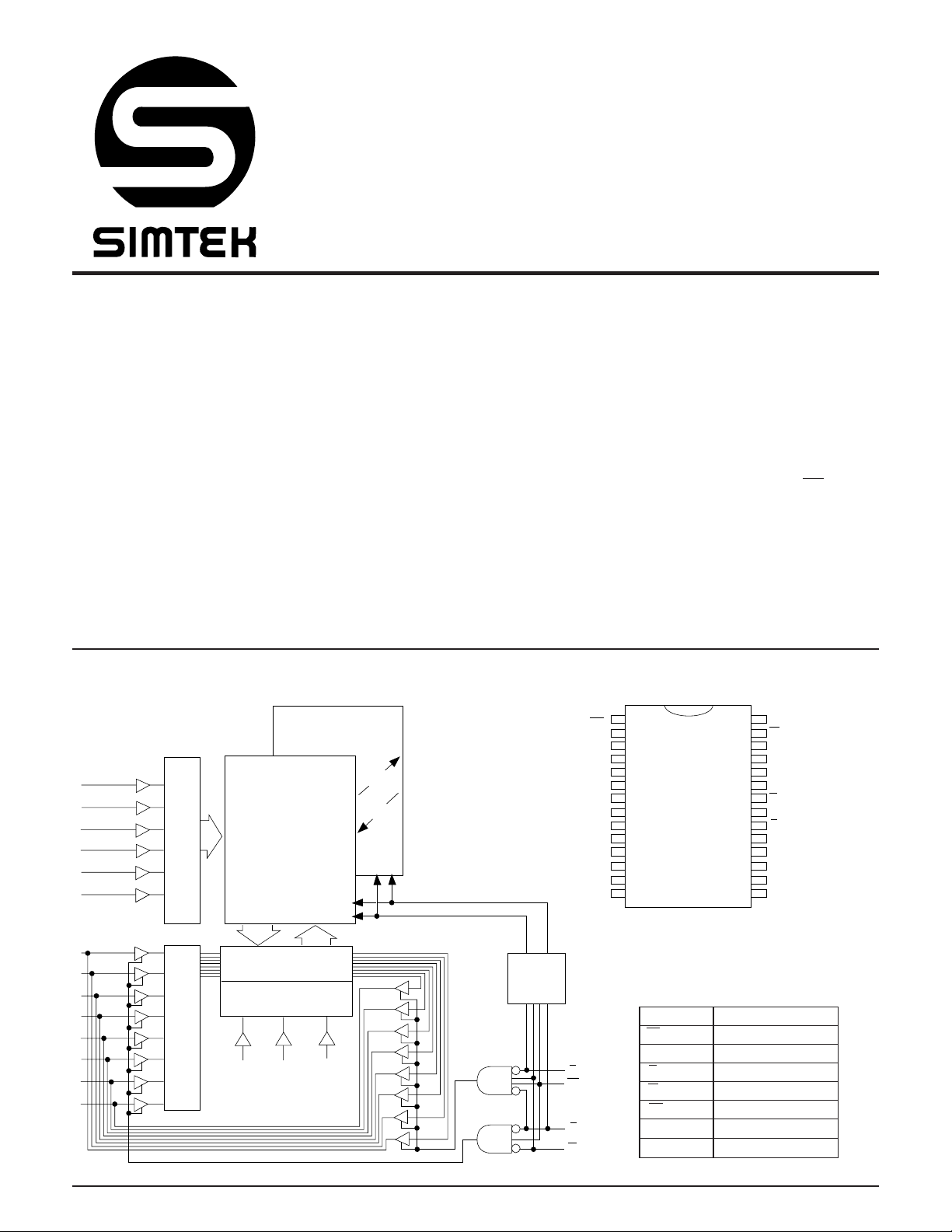
LOGIC BLOCK DIAGRAM
EEPROM ARRAY
64 X 64
A
3
A
4
A
5
A
6
A
7
A
8
ROW DECODER
STATIC RAM
ARRAY
64 X 64
STORE
RECALL
DESCRIPTION
The Simtek STK20C04 is a fast static RAM (30, 35,
45ns), with a nonvolatile electrically-erasable PROM
(EEPROM) element incorporated in each static memory
cell. The SRAM can be read and written an unlimited
number of times, while independent nonvolatile data
resides in EEPROM. Data may easily be transferred
from the SRAM to the EEPROM (
EEPROM to the SRAM (
RECALL
STORE
), or from the
) using the NE pin. It
combines the high performance and ease of use of a
fast
SRAM with nonvolatile data integrity.
The STK20C04 features the industry standard pinout
for nonvolatile RAMs in a 28-pin 600 mil plastic DIP.
PIN CONFIGURATIONS
DQ
DQ
DO
1
NE
2
NC
3
A
7
4
A
6
5
A
5
6
A
4
7
A
3
8
A
2
9
A
1
10
A
0
11
0
12
1
13
2
14
V
SS
28
V
CC
W
27
26
NC
25
A
8
24
NC
NC
23
22
G
21
NC
20
E
DQ
19
18
17
16
15
DQ
DQ
DQ
DQ
7
6
5
4
3
DQ
DQ
DQ
DQ
DQ
DQ
DQ
DQ
28 - 600 PDIP
0
1
2
3
4
5
6
7
INPUT BUFFERS
COLUMN I/O
COLUMN DECODER
AA A
01
2
STORE/
RECALL
CONTROL
NE
PIN NAMES
A0 - A
W Write Enable
DQ0 - DQ7Data In/Out
G
E
W
E Chip Enable
G Output Enable
NE Nonvolatile Enable
V
CC
V
SS
8
Address Inputs
Power (+5V)
Ground
2-39
STK20C04
ABSOLUTE MAXIMUM RATINGS
Voltage on typical input relative to V
Voltage on DQ
and G. . . . . . . . . . . . . . . . . . .–0.5V to (VCC+0.5V)
0-7
Temperature under bias . . . . . . . . . . . . . . . . . . . . . . –55°C to 125°C
Storage temperature. . . . . . . . . . . . . . . . . . . . . . . . . –65°C to 150°C
Power dissipation. . . . . . . . . . . . . . . . . . . . . . . . . . . . . . . . . . . . . .1W
DC output current . . . . . . . . . . . . . . . . . . . . . . . . . . . . . . . . . . .15mA
. . . . . . . . . . . . . –0.6V to 7.0V
SS
a
Note a: Stresses greater than those listed under "Absolute Maximum
Ratings" may cause permanent damage to the device. This is a stress
rating only, and functional operation of the device at conditions above
those indicated in the operational sections of this specification is not
implied. Exposure to absolute maximum rating conditions for extended
periods may affect reliability.
(One output at a time, one second duration)
DC CHARACTERISTICS (VCC = 5.0V ± 10%)
SYMBOL PARAMETER UNITS NOTES
b
I
CC
I
CC
I
SB
I
SB
I
ILK
I
OLK
V
V
V
V
T
1
2
1
2
IH
IL
OH
OL
A
Average VCC Current 80 85 mA t
d
Average VCC Current 50 50 mA All inputs at
STORE
during
c
Average VCC Current 27 30 mA t
(Standby, Cycling TTL Input Levels) 23 27 mA t
c
Average VCC Current 1 1 mA E ≥ (VCC – 0.2V)
(Standby, Stable CMOS Input Levels) all others V
Input Leakage Current (Any Input) ±1 ±1 µAVCC = max
Off State Output Leakage Current ±5 ±5 µAVCC = max
Input Logic "1" Voltage 2.2 VCC+.5 2.2 VCC+.5 V All Inputs
Input Logic "0" Voltage VSS–.5 0.8 VSS–.5 0.8 V All Inputs
Output Logic "1" Voltage 2.4 2.4 V I
Output Logic "0" Voltage 0.4 0.4 V I
Operating Temperature 0 70 –40 85 °C
cycle VIN ≤ 0.2V or ≥ (VCC – 0.2V)
COMMERCIAL INDUSTRIAL
MIN MAX MIN MAX
75 80 mA t
65 75 mA t
20 23 mA t
= 30ns
AVAV
= 35ns
AVAV
= 45ns
AVAV
= 30ns
AVAV
= 35ns
AVAV
= 45ns
AVAV
; all others cycling
E ≥ V
IH
= VSS to V
V
IN
= VSS to V
V
IN
= –4mA
OUT
= 8mA
OUT
≤ 0.2V or ≥ (VCC – 0.2V)
IN
CC
CC
Note b: ICC is dependent on output loading and cycle rate. The specified values are obtained with outputs unloaded.
Note c: Bringing E ≥ VIH will not produce standby current levels until any nonvolatile cycle in progress has timed out. See MODE SELECTION table.
Note d: I
1
is the average current required for the duration of the store cycle (t
CC
2
) after the sequence (tWC) that initiates the cycle.
STORE
AC TEST CONDITIONS
Input Pulse Levels. . . . . . . . . . . . . . . . . . . . . . . . . . . . . VSS to 3V
Input Rise and Fall Times. . . . . . . . . . . . . . . . . . . . . . . . . . ≤ 5ns
Input and Output Timing Reference Levels. . . . . . . . . . . . . . 1.5V
Output Load. . . . . . . . . . . . . . . . . . . . . . . . . . . . . . . See Figure 1
CAPACITANCE (T
SYMBOL PARAMETER MAX UNITS CONDITIONS
C
IN
C
OUT
Note e: These parameters are guaranteed but not tested.
Input Capacitance 7 pF ∆V = 0 to 3V
Output Capacitance & W 7 pF ∆V = 0 to 3V
=25°C, f=1.0MHz)
A
e
Output
255 Ohms
Figure 1: AC Output Loading
5.0V
480 Ohms
INCLUDING
AND FIXTURE
30pF
SCOPE
2-40
STK20C04
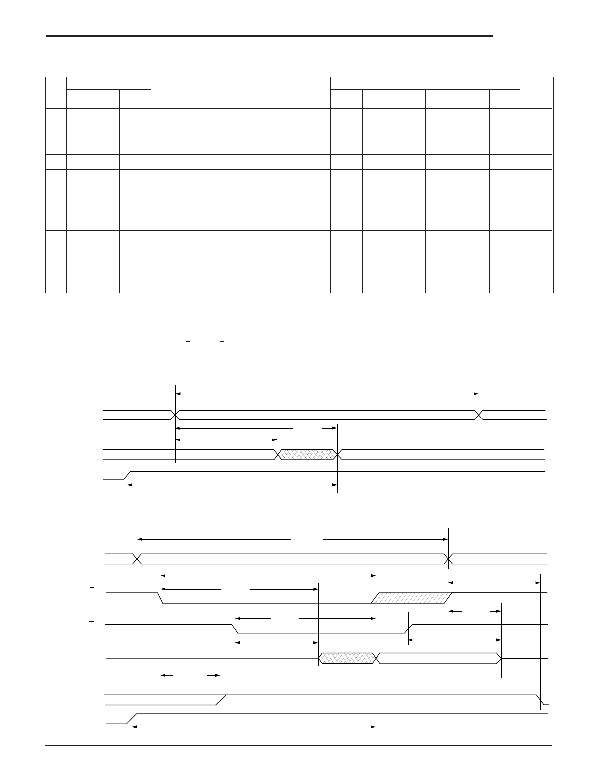
READ CYCLES #1 & #2
(VCC = 5.0V ± 10%)
SYMBOLS STK20C04-30 STK20C04-35 STK20C04-45
NO. PARAMETER UNITS
1t
2t
3t
4t
5t
6t
7t
8t
9t
10 t
11 t
11A t
#1, #2 Alt. MIN MAX MIN MAX MIN MAX
t
ELQV
AVAVR
AVQV
GLQV
AXQX
ELQX
EHQZ
GLQX
GHQZ
ELICCH
EHICCL
WHQV
g
h
i
i
e
c,e
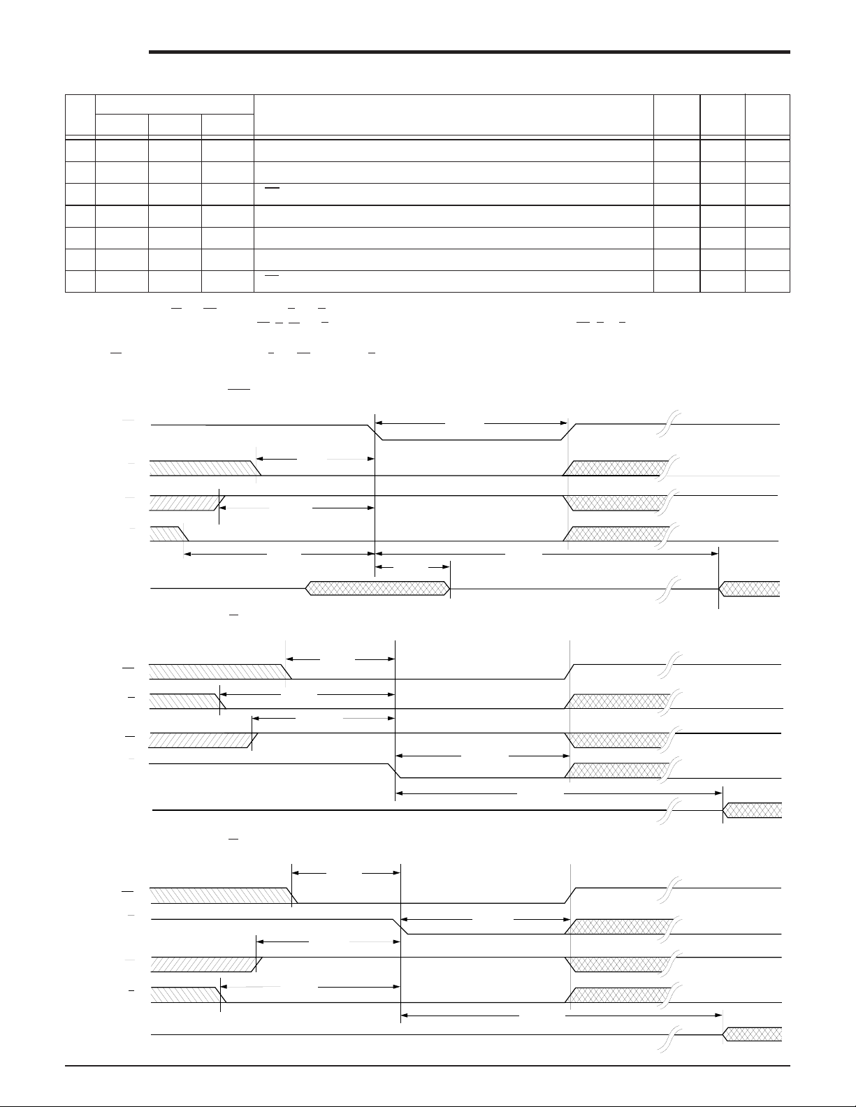
Chip Enable Access Time 30 35 45 ns
ACS
t
Read Cycle Time 30 35 45 ns
RC
t
Address Access Time 30 35 45 ns
AA
t
Output Enable to Data Valid 15 20 25 ns
OE
t
Output Hold After Address Change 5 5 5 ns
OH
t
Chip Enable to Output Active 5 5 5 ns
LZ
t
Chip Disable to Output Inactive 18 20 25 ns
HZ
t
Output Enable to Output Active 0 0 0 ns
OLZ
t
Output Disable to Output Inactive 18 20 25 ns
OHZ
t
Chip Enable to Power Active 0 0 0 ns
PA
t
Chip Disable to Power Standby 25 25 25 ns
PS
t
Write Recovery Time 35 45 55 ns
WR
Note c: Bringing E high will not produce standby currents until any nonvolatile cycle in progress has timed out. See MODE SELECTION table.
Note e: Parameter guaranteed but not tested.
Note f: NE must be high during entire cycle.
Note g: For READ CYCLE #1 and #2, W and NE must be high for entire cycle.
Note h: Device is continuously selected with E low and G low.
Note i: Measured ± 200mV from steady state output voltage.
f,g,h
READ CYCLE #1
2
t
AVAVR
ADDRESS
3
t
AVQV
DATA VALID
DQ (Data Out)
t
AXQX
5
W
READ CYCLE #2
ADDRESS
E
G
DQ (Data Out)
I
CC
W
ACTIVE
STANDBY
f,g
10
t
ELICCH
11A
t
WHQV
t
6
ELQX
11A
t
WHQV
t
GLQX
8
t
ELQV
t
GLQV
t
AVAVR
1
4
2-41
2
11
t
EHICCL
7
t
EHQZ
9
t
GHQZ
DATA VALID
STK20C04
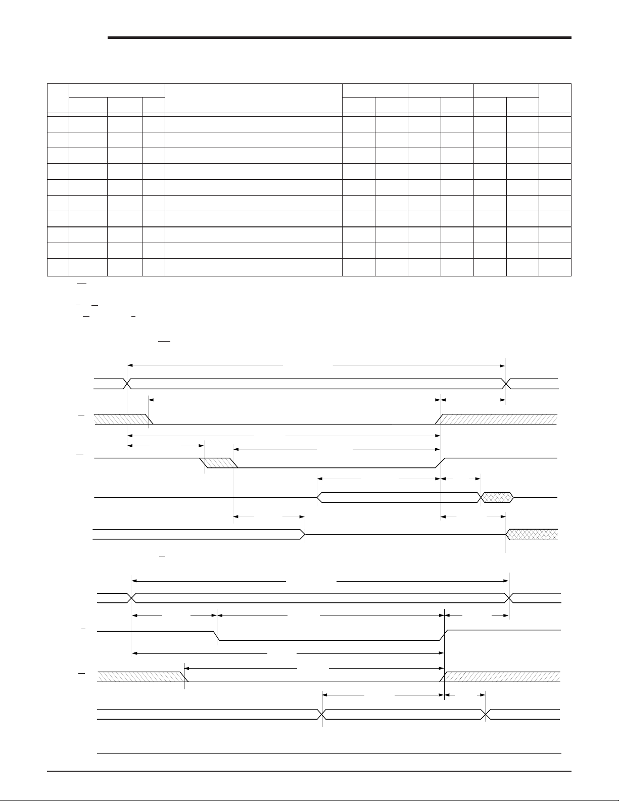
WRITE CYCLES #1 & #2
(VCC = 5.0V ± 10%)
SYMBOLS STK20C04-30 STK20C04-35 STK20C04-45
NO. PARAMETER UNITS
12 t
13 t
14 t
15 t
16 t
17 t
18 t
19 t
20 t
21 t
#1 #2 #3 MIN MAX MIN MAX MIN MAX
AVAVWtAVAVWtWC
WLWHtWLEHtWP
i,m
t
ELEHtCW
t
AVELtAS
ELWH
DVWHtDVEHtDW
WHDXtEHDXtDH
AVWHtAVEHtAW
AVWL
WHAXtEHAXtWR
WLQZ
WHQX
Write Cycle Time 45 45 45 ns
Write Pulse Width 35 35 35 ns
Chip Enable to End of Write 35 35 35 ns
Data Set-up to End of Write 30 30 30 ns
Data Hold After End of Write 0 0 0 ns
Address Set-up to End of Write 35 35 35 ns
Address Set-up to Start of Write 0 0 0 ns
Address Hold After End of Write 0 0 0 ns
tWZWrite Enable to Output Disable 35 35 35 ns
tOWOutput Active After End of Write 5 5 5 ns
Note f: NE must be high during entire cycle.
Note i: Measured ± 200mV from steady state output voltage.
Note k: E or W must be high during address transitions.
Note m: If W is low when E goes low, the outputs remain in the high impedance state.
WRITE CYCLE #1: W CONTROLLED
f,k
12
t
AVAVW
ADDRESS
14
t
ELWH
19
t
WHAX
E
17
t
AVWH
20
t
WLQZ
13
t
WLWH
15
t
DVWH
DATA VALID
HIGH IMPEDANCE
16
t
WHDX
21
t
WHQX
DATA IN
DATA OUT
18
t
W
AVWL
PREVIOUS DATA
WRITE CYCLE #2: E CONTROLLED
ADDRESS
18
t
AVEL
E
W
DATA IN
DATA OUT
f,k
12
t
AVAVW
14
t
ELEH
17
t
AVEH
t
WLEH
HIGH IMPEDANCE
2-42
13
15
t
DVEH
DATA VALID
16
t
EHDX
19
t
EHAX

NONVOLATILE MEMORY OPERATION
MODE SELECTION
E W G NE MODE POWER
H X X X Not Selected Standby
L H L H Read RAM Active
L L X H Write RAM Active
L H L L Nonvolatile
L L H L Nonvolatile
L L L L No operation Active
LHHX
RECALL
STORE
n
STK20C04
Active
I
CC
2
STORE CYCLES #1 & #2
NO. PARAMETER MIN MAX UNITS
22 t
23 t
24 t
25 t
26 t
27 t
28 t
Note: n: An automatic
VCC must not drop below 3.8V once it has exceeded it for the
Note o: If E is low for any period of time in which W is high while G and NE are low, then a
Note p: Measured with W and NE both returned high, and G returned low. Note that
Note q: Once tWC has been satisfied by NE, G, W and E, the
STORE CYCLE #1: W CONTROLLED
DQ (Data Out)
SYMBOLS
#1 #2 Alt.
p
WLQX
WLNH
GHNL
NLWL
ELWL
t
ELQXS
q
t
ELNHS
GHEL
t
NLEL
WLEL
RECALL
STORE
initiation cycle.
NE
G
W
E
t
STORE
t
WC
also takes place at power up, starting when VCC exceeds 3.8V, and taking t
STORE
Cycle Time 10 ms
STORE
Initiation Cycle Time 45 ns
Output Disable Set-up to NE Fall 0 ns
Output Disable Set-up to E Fall 0 ns
NE Set-up 0ns
Chip Enable Set-up 0ns
Write Enable Set-up 0 ns
RECALL
to function properly.
RECALL
cycle may be initiated.
STORE
cycles are inhibited/aborted by V
STORE
cycle is completed automatically. Any of NE, G, W or E may be used to terminate the
o
24
t
GHNL
27
t
ELWL
HIGH IMPEDANCE
26
t
NLWL
23
t
WLNH
22
t
WLQX
from the time at which VCC exceeds 4.5V.
RECALL
(VCC = 5.0V ± 10%)
< 3.8V (
STORE
CC
inhibit).
STORE CYCLE #2: E CONTROLLED
NE
25
t
GHEL
G
28
t
W
DQ (Data Out)
E
HIGH IMPEDANCE
WLEL
o
26
t
NLEL
2-43
t
ELNHS
22
t
ELQXS
23
STK20C04
RECALL CYCLES #1, #2 & #3
(VCC = 5.0V ± 10%)
SYMBOLS
NO. PARAMETER MIN MAX UNITS
29 t
30 t
31 t
32 t
33 t
34 t
35 t
#1 #2 Alt.
r
NLQX
NLNH
GLNL
WHNL
ELNL
NLQZ
t
ELQXRtGLQXR
s
t
ELNHRtGLNH
NLEL
t
GLEL
t
WHELtWHGL
t
NLGL
t
ELGL
RECALL
Cycle Time 20 µs
RECALL
Initiation Cycle Time 25 ns
NE Set-up 0ns
Output Enable Set-up 0 ns
t
Write Enable Set-up 0 ns
Chip Enable Set-up 0ns
NE Fall to Outputs Inactive 25
ns
Note r: Measured with W and NE both high, and G and E low.
Note s: Once t
RECALL
Note t: If W is low at any point in which both E and NE are low and G is high, then a
RECALL CYCLE #1: NE CONTROLLED
has been satisfied by NE, G, W and E, the
NLNH
initiation cycle.
NE
G
32
t
GLNL
RECALL
cycle is completed automatically. Any of NE, G or E may be used to terminate the
STORE
cycle will be initiated instead of a
RECALL.
o
30
t
NLNH
W
E
DQ (Data Out)
t
34
t
ELNL
33
WHNL
RECALL CYCLE #2: E CONTROLLED
31
t
32
t
GLEL
33
t
WHEL
NLEL
NE
DQ (Data Out)
G
W
E
HIGH IMPEDANCE
RECALL CYCLE #3: G CONTROLLED
31
t
NLGL
NE
G
33
t
WHGL
W
34
t
E
DQ (Data Out)
ELGL
HIGH IMPEDANCE
o
o,t
35
t
NLQZ
30
t
ELNHR
t
30
GLNH
t
NLQX
29
t
ELQXR
t
GLQXR
29
29
HIGH IMPEDANCE
2-44

DEVICE OPERATION
STK20C04
The STK20C04 has two modes of operation: SRAM
mode and nonvolatile mode, determined by the state of
the NE pin. When in
as an ordinary static
data is transferred in parallel from
from
EEPROM to SRAM.
SRAM mode, the memory operates
RAM. While in nonvolatile mode,
SRAM to EEPROM or
SRAM READ
The STK20C04 performs a READ cycle whenever E
and G are
specified on pins A
data bytes will be accessed. When the
LOW and NE and W are HIGH. The address
determines which of the 512
0-8
READ is initiated
by an address transition, the outputs will be valid after
a delay of t
initiated by E or G, the outputs will be valid at t
at t
whichever is later (READ CYCLE #2). The data
GLQV
(READ CYCLE #1). If the READ is
AVQV
ELQV
or
outputs will repeatedly respond to address changes
within the t
access time without the need for
AVQV
transitions on any control input pins, and will remain
valid until another address change or until E or G is
brought
HIGH or W or NE is brought LOW.
SRAM WRITE
A write cycle is performed whenever E and W are LOW
and NE is HIGH. The address inputs must be stable
prior to entering the
stable until either E or W go
cycle. The data on pins DQ
memory if it is valid t
controlled
controlled
WRITE or t
WRITE.
It is recommended that G be kept
WRITE cycle to avoid data bus contention on common
I/O lines. If G is left
the output buffers t
WRITE cycle and must remain
HIGH at the end of the
will be written into the
0-7
before the end of a W
DVWH
before the end of an E
DVEH
HIGH during the entire
LOW, internal circuitry will turn off
after W goes LOW.
WLQZ
NONVOLATILE STORE
A
STORE
LOW and G is HIGH. While any sequence to achieve
this state will initiate a
CYCLE #1) and E initiation (
practical without risking an unintentional
that would disturb SRAM data. During a
previous nonvolatile data is erased and the
contents are then programmed into nonvolatile elements. Once a
cycle is performed when NE, E and W are
STORE
STORE
, only W initiation (
STORE
CYCLE #2) are
STORE
STORE
SRAM WRITE
cycle,
SRAM
cycle is initiated, further input
and output is disabled and the DQ
pins are tri-stated
0-7
until the cycle is completed.
If E and G are LOW and W and NE are HIGH at the end
of the cycle, a
will go active, signaling the end of the
READ will be performed and the outputs
STORE
.
HARDWARE PROTECT
The STK20C04 offers two levels of protection to suppress inadvertent
(E, G, W, and NE) remain in the
end of a
STORE
be started. The
STORE
cycles. If the control signals
STORE
cycle, a second
STORE
(or
RECALL
condition at the
STORE
cycle will
) will be initiated
not
only after a transition on any one of these signals to the
required state. In addition to multi-trigger protection,
the STK20C04 offers hardware protection through V
Sense. A
progress will discontinue if V
STORE
cycle will not be initiated, and one in
goes below 3.8V. 3.8V
CC
CC
is a typical, characterized value.
NONVOLATILE RECALL
A
RECALL
LOW and W is HIGH. Like the
initiated when the last of the four clock signals goes to
the
RECALL
take t
ignored. When the
WRITE state on the input pins will take effect.
Internally,
SRAM data is cleared and second, the nonvolatile
information is transferred into the
RECALL
nonvolatile cells. The nonvolatile data can be recalled
an unlimited number of times.
Like the
control pin to cause a recall, preventing inadvertent
multi-triggering. On power-up, once V
V
CC
cally initiated. The voltage on the V
below 3.8V once it has risen above it in order for the
RECALL
RECALL
after VCC exceeds 3.8V. 3.8V is a typical, characterized value.
cycle is performed when E, G, and NE are
STORE
state. Once initiated, the
to complete, during which all inputs are
NLQX
RECALL
RECALL
is a two step procedure. First, the
completes, any READ or
cycle,
RECALL
SRAM cells. The
RECALL
operation in no way alters the data in the
STORE
sense voltage of 3.8V, a
cycle, a transition must occur on any
exceeds the
CC
RECALL
cycle is automati-
pin must not drop
CC
to operate properly. Due to this automatic
, SRAM operation cannot commence until t
is
cycle will
NLQX
2-45

STK20C04
ORDERING INFORMATION
STK20C04 - W 30 I
Temperature Range
blank = Commercial (0 to 70 degrees C)
I = Industrial (–40 to 85 degrees C)
Access Time
30 = 30ns
35 = 35ns
45 = 45ns
Package
W = Plastic 28 pin 600 mil DIP
2-46
 Loading...