

STK1743
8K x 8
FEATURES
• Data Integrity of Simtek nvSRAM Combined
with Full-Featured Real-Time Clock
• Stand-Alone Nonvolatile Memory and TimeKeepin g S olution—No Other Parts Required
• No Batteries to Fail
• Fast 25ns, 35ns and 45ns Access Times
• Software- and
AutoStore
Nonvolatile Cycles
• Year 2000 Compliant with Leap Year
Compensation
• 24-Hour BCD Format
• 100-Y ear Data Retention over Full Industrial
Temperature Range
• Full 30-Day RTC Operation on Each Power
Loss
• Single 5V ± 10% Power Supply
™-Controlled
AutoStore
nvTime
™ nvSRAM
™
with Real-Time Clock
ADVANCE
DESCRIPTION
The Simtek STK1743 DIP module houses 64Kb of
nonvolatile static
crystal and a high-value capacitor to support systems that require high reliability and ease of manufacturing.
READ and WRITE access to all RTC
functions and the memory is the same as a conventional x 8
RAM support clock registers for centuries, years,
SRAM. The highest eight addresses of the
months, dates, days, hours, minutes and seconds.
Independent data resides in the integral
all times. Automatic
the
EEPROM data to the SRAM, while an automatic
STORE
on power down transfers SRAM data to the
EEPROM. A software
possible on user command.
ited accesses to
STORE
s.
RAM, a real-time clock (RTC) with
EEPROM at
RECALL
RECALL
SRAM, unlimited
on power up transfers
and
nvTime
STORE
™ allows unlim-
RECALL
are also
s and 10
6
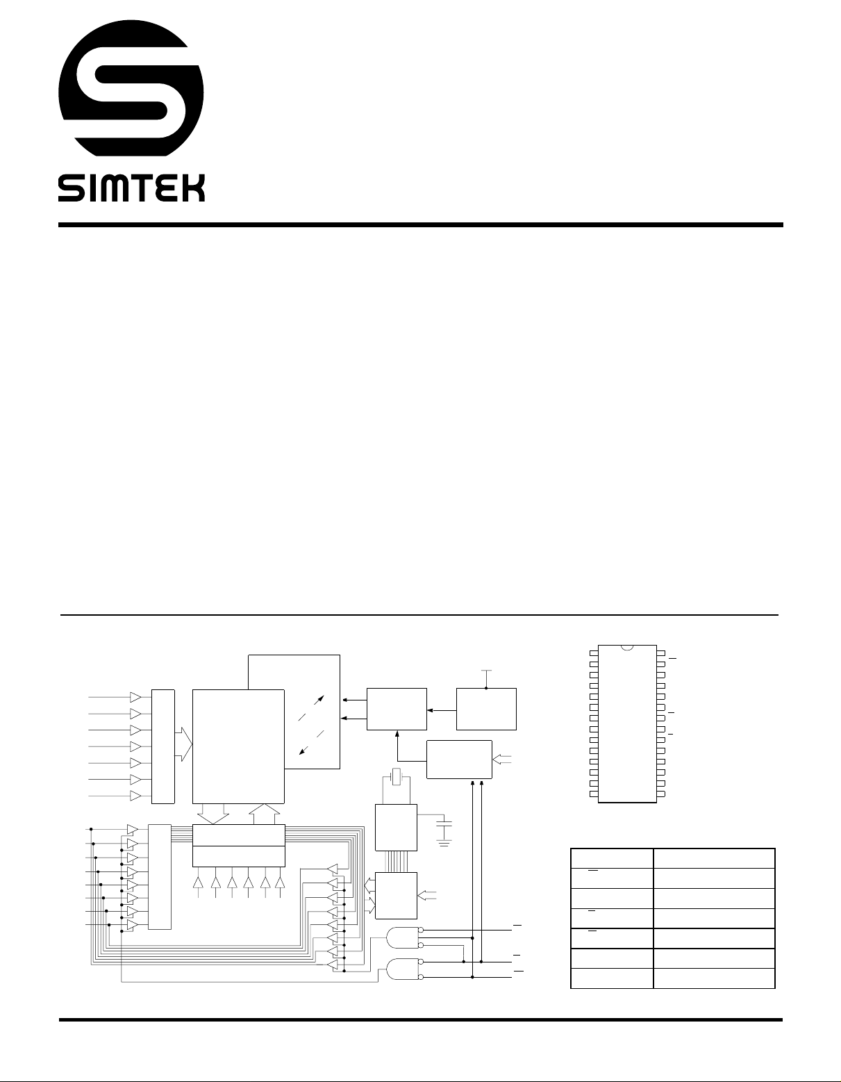
BLOCK DIAGRAM
A
5
A
6
A
7
A
8
A
9
A
DQ
DQ
DQ
DQ
DQ
DQ
DQ
DQ
11
A
12
0
1
2
3
4
5
6
7
ROW DECOD ER
COLUMN DEC
A0A
INPUT BUFFERS
EEPROM ARRAY
STATIC RAM
ARRA Y
128 x 512
CO L UM N I/O
A3A
2
1
128 x 512
A
A
10
4
STORE
RECALL
STORE/
RECALL
CONTROL
RTC
MUX
POWER
CONTROL
SOFTW ARE
DETECT
A0 A
12
PIN CONFIGURATIONS
NC
DQ
DQ
DQ
V
1
2
A
12
3
A
7
A
4
6
A
5
5
A
6
4
A
7
3
8
A
2
9
A
1
10
A
0
11
0
12
1
13
2
14
SS
V
CC
A0 - A
12
28
V
CC
27
W
26
NC
25
A
8
A
24
9
23
A
11
22
G
21
A
10
20
E
19
DQ
7
DQ
DQ
DQ
DQ
6
5
4
3
600 mil
Dual
In-Line
Module
18
17
16
15
PIN NAM ES
A0 - A
12
W
- DQ
DQ
0
E
G
E
W
G
V
CC
V
SS
7
Address I nputs
Write E nable
Data In/Out
Chip Enable
Output Enable
Power (+ 5V)
Ground
March 1999 7-1
STK1743
ABSOLUTE MAXIMUM RATINGS
a
Voltage on Inpu t Relative to VSS . . . . . . . . . .–0.6V to (VCC + 0.5V)
Voltage on DQ
. . . . . . . . . . . . . . . . . . . . . .–0.5V to (VCC + 0.5V)
0-7
Temperature under Bias. . . . . . . . . . . . . . . . . . . . . –55°C to 125°C
Storage Temperature . . . . . . . . . . . . . . . . . . . . . . . –65°C to 150°C
Power Dissipation. . . . . . . . . . . . . . . . . . . . . . . . . . . . . . . . . . . . 1W
DC Output Current (1 output at a time, 1s duration ) . . . . . . . 15mA
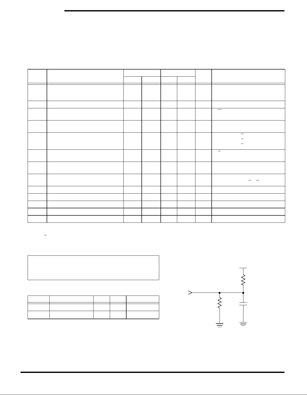
DC CHARAC TERISTICS (VCC = 5.0V ± 10%)
Note a: Stresses greater than those listed under “Absolute Maxi-
mum Ratings” may cause permanent damage to the device.
This a stress rating only, and functional operation of the
device at conditions above those indicated in the operational sections of this specification is not implied. Exposure
to absolute maximum rating conditions for extended periods
may affect reliability.
SYMBOL PARAMETER
b
I
CC
I
CC
I
CC
I
CC
I
SB
I
SB
I
ILK
I
OLK
V
IH
V
IL
V
OH
V
OL
T
A
Note b: I
Note c: I
Note d: E ≥ VIH will not produce standby current levels until any nonvolatile cycle in progress has timed out.
Average VCC Current 85
1
c
Average VCC Current during
2
b
Average VCC Current at t
3
c
Average VCC Current during
4
AutoStore
d
Average VCC Current
1
(Standby, Cycling TTL Input Levels)
d
VCC Standby Current
2
(Standby, Stable CMOS Input Lev els)
Input Leakage Current
Off-Stat e Output Leakage Current
Input Logic “ 1” Voltage 2.2 V
Input Logic “ 0” Voltage VSS – .5 0 . 8 VSS – .5 0.8 V All Inputs
Output Logic “1” Voltage 2.4 2.4 V I
Output Logic “0” Vo ltage 0.4 0.4 V I
Operating Temperatur e 0 70 –40 85
and I
CC
1
and I
CC
2
™ Cycle
are dependent on output loading and cycle rate. The specified values are obtained at minimum cycle with outputs unloaded.
CC
3
are the average currents required for the duration of the respective
CC
4
AVAV
STORE
= 200ns
COMMERCIAL INDUSTRIAL
MIN MAX MIN MAX
80
75
67mAAll Inputs Don’t Care, VCC = max
15 15 mA
44mA
30
26
23
33mA
1
±
5
±
+ .5 2.2 VCC + .5 V All Inputs
CC
95
85
80
31
27
24
±
±
1
5
STORE
UNITS NOTES
mA
mA
mA
mA
mA
mA
A
µ
A
µ
C
°
cycles (t
t
= 25ns
AVAV
t
= 35ns
AVAV
t
= 45ns
AVAV
W
≥ (V
– 0.2V)
CC
All Others Cyc ling, CMOS Levels
All Inputs Don’t Care
t
= 25ns, E
AVAV
t
= 35ns, E ≥ V
AVAV
t
= 45ns, E ≥ V
AVAV
E ≥ (VCC – 0.2V)
All Others V
V
= max
CC
V
= VSS to V
IN
V
= max
CC
V
= V
IN
SS
= –4mA
OUT
= 8mA
OUT
).
STORE
V
≥
IH
IH
IH
≤ 0.2V or ≥ (VCC – 0.2V)
IN
CC
to VCC, E or G ≥
V
IH
AC TEST CO NDITIONS
Input Pulse Levels. . . . . . . . . . . . . . . . . . . . . . . . . . . . . . . 0V to 3V
Input Ris e and Fall Times . . . . . . . . . . . . . . . . . . . . . . . . . . . . . . .≤ 5ns
Input and Output Timing Reference Levels. . . . . . . . . . . . . . . .1.5V
Output Load. . . . . . . . . . . . . . . . . . . . . . . . . . . . . . . . . See Figure 1
CAPACITANCE
SYMBOL PARAMETER MAX UNITS CONDITIONS
C
IN
C
OUT
Note e: These parameters are guaranteed but not tested.
Input Capacitance
Output Cap ac itance
e
(TA = 25°C, f = 1.0M Hz)
10 pF
12 pF
∆V = 0 to 3V
∆V = 0 to 3V
March 1999 7-2
OUTPUT
5.0V
480 Ohms
30 pF
255 Ohm s
INCLUDING
SCOPE AND
FIXTURE
Figure 1: AC Output Loading
STK1743
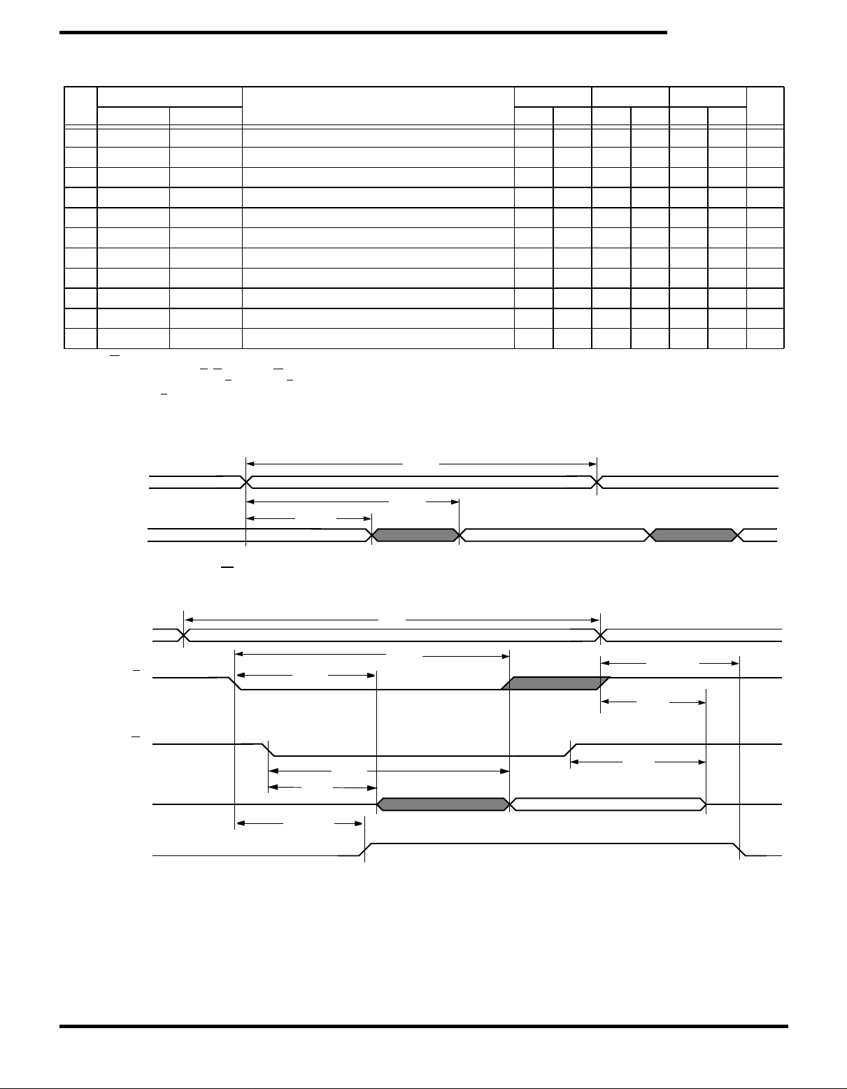
READ CYCLES #1 & #2 (VCC = 5.0V ± 10%)
NO.
10 t
11 t
#1, #2 Alt. MIN MAX MIN MA X MI N M AX
1t
ELQV
2t
AVAV
3t
AVQV
4t
GLQV
5t
AXQX
6t
ELQX
7t
EHQZ
8t
GLQX
9t
GHQZ
ELICCH
EHICCL
SYMBOLS
f
g
g
h
h
e
d, e
t
ACS
t
RC
t
AA
t
OE
t
OH
t
LZ
t
HZ
t
OLZ
t
OHZ
t
PA
t
PS
Chip Enable Access Time 25 35 45 ns
Read Cycle Time 25 35 45 ns
Address Access Time 25 35 45 ns
Output Enable to Data Valid 10 15 20 ns
Output Hold after Address Change 5 5 5 ns
Chip Enable t o Output Activ e 5 5 5 ns
Chip Disable to Output Inac tive 10 13 15 ns
Output Enable to Output Active 0 0 0 ns
Output Disable to Output Inactive 10 13 15 ns
Chip Enable t o P ower Active 0 0 0 ns
Chip Disable to Power Standby 25 35 45 ns
PARAMETER
Note f: W must be high during SRAM READ cycles and low during SRA M WRITE cycles.
Note g: I/O state assumes E, G < VIL and W > VIH; device is continuously selected.
Note h: Measured + 200mV from steady state output voltage.
READ CY C LE #1: Add ress Controlled
f, g
t
AVAV
2
ADDRESS
3
t
t
AXQX
5
AVQV
DQ (DATA OUT)
STK1743-25 STK1743-35 STK1743-45
DATA VALID
UNITS
READ CY C LE #2: E Contro lled
ADDRESS
6
STANDBY
t
ELQX
t
GLQX
10
t
ELICCH
DQ (DATA OUT)
I
CC
E
G
f
2
t
AVAV
1
t
ELQV
4
t
GLQV
8
DATA VALID
ACTIVE
t
GHQZ
9
t
EHQZ
t
7
11
EHICCL
March 1999 7-3

STK1743
WRITE CYCLES #1 & #2 (VCC = 5.0V ± 10%)
NO.
12 t
13 t
14 t
15 t
16 t
17 t
18 t
19 t
20 t
21 t
WLQZ
SYMBOLS
#1 #2 Alt. MIN MAX MIN MAX MIN MAX
AVAV
WLWH
ELWH
DVWH
WHDX
AVWH
AVWL
WHAX
WHQX
h, i
t
AVAV
t
WLEH
t
ELEH
t
DVEH
t
EHDX
t
AVEH
t
AVEL
t
EHAX
t
Write Cycle Time 25 35 45 ns
WC
t
Write Pul s e Width 20 25 30 ns
WP
t
Chip Enable t o E nd of Write 20 25 30 ns
CW
t
Data Set-up to End of Write 10 12 15 ns
DW
t
Data Hold aft er E nd of Write 0 0 0 ns
DH
t
Address Set-up to End of Write 20 25 30 ns
AW
t
Address Set-up to Start of Write 0 0 0 ns
AS
t
Address Hold after End of Write 0 0 0 ns
WR
t
Write Ena ble to Output Dis able 10 13 15 ns
WZ
t
Output Acti v e after En d of Write 5 5 5 ns
OW
PARAMETER
Note i: If W is low when E goes low, the outputs remain in the high-impedance state.
Note j: E or W must be ≥ VIH during address transitions.
WRITE CYCLE #1: W Controlled
j
12
t
AVAV
ADDRESS
14
t
ELWH
E
STK1743-25 STK1743-35 STK1743-45
19
t
WHAX
UNITS
18
t
AVWL
W
DATA IN
t
WLQZ
DAT A OUT
PREVIOUS DAT A
WRITE CYCLE #2: E Controlled
ADDRESS
18
t
AVEL
E
W
DATA IN
20
17
t
AVEH
j
17
t
AVWH
13
t
WLWH
12
t
AVAV
14
t
ELEH
13
t
WLEH
15
t
DVWH
DATA VAL ID
HIGH IMPEDENCE
15
t
DVEH
DATA VAL ID
16
t
WHDX
t
EHAX
t
EHDX
21
t
WHQX
19
16
DAT A OUT
HIGH IMPEDENCE
March 1999 7-4

STK1743
AutoStore
NO.
22 t
23 t
24 t
25 V
26 V
Note k: t
SYMBOLS
RESTORE
STORE
DELAY
SWITCH
RESET
RESTORE
AutoStore
25
V
SWITCH
26
V
RESET
AutoStore
™ / POWER-UP
Standard MIN MAX
Power-Up
STORE
Time Allowed to Complete SRAM Cycle 1
Low Voltage Trigger Level 4.0 4.5 V
Low Voltage Reset Level 3.9 V
starts from the time VCC rises above V
™ / POWER-UP
V
CC
5V
™
RECALL
PARA METER
RECALL
Duration 550
Cycle Duration 10 ms g
.
SWITCH
(VCC = 5.0V ± 10%)
STK1743
RECALL
23
t
STORE
UNITS NOTES
sk
µ
sg
µ
POWER-UP
DQ (DATA OUT)
RECALL
W
POWER-UP
22
t
RESTORE
RECALL
BROWN OUT
NO
STORE
DUE TO
NO SRAM WRITES
NO
RECALL
(VCC DID NOT GO
BELOW V
RESET
24
t
DELAY
BROWN OUT
AutoStore
NO
™
RECALL
(VCC DID NOT GO
)
BELOW V
RESET
)
BROWN OUT
AutoStor e
RECALL
V
ABOVE V
RETURNS
CC
WHEN
SWITCH
™
March 1999 7-5

STK1743
SOFTW ARE MODE SELECTION
E W A12 - A0 (hex) MODE I/O NOTES
0000
1555
LH
LH
0AAA
1FFF
10F0
0F0F
0000
1555
0AAA
1FFF
10F0
0F0E
Note l: The six consecutive addresses must be in the order listed. W must be high during all six consecutive cycles to enable a nonvolatile cycle.
Read SRAM
Read SRAM
Read SRAM
Read SRAM
Read SRAM
Nonvolat ile
Read SRAM
Read SRAM
Read SRAM
Read SRAM
Read SRAM
Nonvolat ile
STORE
RECALL
Output Data
Output Data
Output Data
Output Data
Output Data
Output High Z
Output Data
Output Data
Output Data
Output Data
Output Data
Output High Z
l
l
SOFTWARE CYCLES #1 & #2
SYMBOLS
NO.
27 t
28 t
29 t
30 t
31 t
#1 MIN MAX MIN MAX MIN MAX
AVAV
m
AVEL
m
ELEH
g, m
ELAX
RECALL
STORE/RECALL
Address Set-up Time 0 0 0 ns
Clock Pulse Width 20 25 30 ns
Address Hold Time 20 20 20 ns
RECALL
Duration 20 20 20
PARAMETER
Initiatio n Cy c le Ti m e 25 35 45 ns
m, n
(VCC = 5.0V ± 10%)
STK1743-25 STK1743-35 STK1743-45
UNITS
s
µ
Note m: The software sequence is clocked with E controlled reads.
Note n: The six consecutive addresses must be in the order listed in the Software Mode Selection Table: (0000, 1555, 0AAA, 1FFF, 10F0, 0F0F) for a
STORE
cycle or (0000, 1555, 0AAA, 1FFF, 10F0, 0F0E) for a
RECALL
cycle. W must be high during all six consecutive cycles.
SOFTWARE CYCLE: E Controlled
ADDRESS
27
t
AVAV
28
t
AVEL
E
t
ELEH
29
27
t
AVAV
ADDRESS #6ADDRESS #1
30
t
ELAX
DQ (DATA OUT)
DATA VALID
March 1999 7-6
DATA VALID
23 31
t
/ t
STORE
HIGH IMPEDENCE
RECALL

DEVICE OPERATION
STK1743
The STK1743 is an 8K x 8 nonvolatile static RAM
with a full-function real-time clock (RTC). The data
integrity is secured in
EEPROM, not subject to bat-
tery or capacitor discharge. The real-time clock registers reside in the eight uppermost
RAM locations,
and contain century, year, month, date, day, hour,
minute and second data in 24-hour
BCD format. Cor-
rections for the day of the month and leap years are
made automatically. This nonvolatile time-keeping
RAM is functionally similar to any JEDEC standard
8K x 8
The
SRAM.
RTC registers are double-buffered to avoid
access of incorrect data that could otherwise occur
during clock update cycles. The double-buffered
system prevents time loss by maintaining internal
clock operation while time register data is accessed.
The STK1743 contains integral power-fail circuitry
that deselects the device when V
V
SWITCH
.
drops below
CC
The STK1743 is a pin-compatible replacement for
the ST Microelectronics M48T08 and the Dallas
Semiconductor DS1743, but without the limitations
of an embedded lithium battery. The Simtek device
uses a double-layer high-value capacitor to maintain
RTC operation on power down for at least 30 days.
The part can be soldered directly onto printed circuit
boards and handled without concern for damaging
or discharging internal batteries. Unlike some other
RTCs, the STK1743 is Year 2000-compliant.
NOISE CONSI DERATI ONS
Note that the STK1743 is a high-speed memory and
so must have a high-frequency bypass capacitor of
approximately 0.1µF connected between V
V
, using leads and traces that are as short as pos-
SS
sible. As with all high-speed
CMOS ICs, normal care-
CC
and
ful routing of power, ground and signals will help
prevent noise problems.
SRAM AND RT C READ
The STK1743 performs a READ cycle whenever E
and G are low and W is high. The address specified
on pins A
bytes will be accessed. When the
by an address transition, the outputs will be valid
after a delay of t
initiated by E
at t
, whichever is later (READ cycle #2). The dat a
GLQV
outputs will repeatedly respond to address changes
within the t
sitions on any control input pins, and will remain valid
until another address change or until E
brough t high or W
Note that the eight most significant bytes of the
address space are reserved for accessing the RTC
registers, as shown in the Register Map below.
While the double-buffered
reduces the chance of reading incorrect data from the
clock, the user should halt internal updates to the
determines which of the 8,192 data
0-12
READ is initiated
(READ cycle #1). If the READ is
AVQV
or G, the outputs will be valid at t
access time without the need for tran-
AVQV
or G is
is brought low.
RTC register structure
ELQV
or
RTC REGISTER MAP
ADDRESS
(HEXADECIMAL)
1FF8 W R 10 Centurie s Centuri es Centuri es : 00-39, Control
1FF9 X 10 Seconds Seconds Seconds: 00 - 59
1FFA X 10 Minutes Minutes Minutes: 00 - 59
1FFB X X 10 Hours Hours Hours: 00 - 23
1FFC 1 FT X X X Days Days: 01 - 07
1FFD X X 10 Dates Dates Dates: 01 - 31
1FFE X X X 10 Mos. Months Months: 01 - 12
1FFF 10 Years Years Years: 00 - 99
Key: R = Read Bit
W = Write Bit
1 = Battery Flag High (no battery to fail)
FT = Frequency T est Bit
X = Don’t Care
D7 D6 D5 D4 D3 D2 D1 D0
BCD DATA
FUNCTION/RANGE
March 1999 7-7

STK1743
STK1743 clock registers before reading clock data
to prevent reading of data in transition. Stopping the
internal register updates does not affect clock accuracy.
The updating process is stopped by writing a “1” to
the read bit (the seventh most s ignificant bit in the
control register), and will not restart until a “0” is
written to the read bit. The
RTC registers can then
be read while the internal clock continues to run.
Within one second after a “0” is written to the read
bit, all STK1743 registers are simultaneously
updated.
SRAM WRITE AND SETTING THE CLOCK
A WRITE cycle is performed whenever E and W are
low. The address inputs must be stable prior to
entering the
until either E
The data on the common I/O pins DQ
ten into the memory if it is valid t
of a W
an E
controlled WRITE.
It is recommended that G
entire
WRITE cycle to avoid data bus contention on
the common I/O lines. If G
cuitry will turn off the output buffers t
WRITE cycle and must remain stable
or W goes high at the end of the cycle.
0-7
before the end
DVWH
controlled WRITE or t
before the end of
DVEH
be kept high during the
is left low, internal cir-
will be writ-
after W
WLQZ
goes low.
Setting the write bit (the eighth most significant bit
of the control register) to a “1” halts updates to the
STK1743 registers. The correct day, date and time
can then be written into the registers in 24-hour
BCD format. Resetting the write bit to “0” transfers
those values to the actual clock counters, after
which the clock resumes normal operation.
CLOCK ACC URACY
The STK1743 is guaranteed to be accurate to
within ± 1 minute per month at 25
requires no additional calibration, and temperature
variations will have a negligible effect in most applications.
°C. The part
write protection occurs), access to the internal clock
register and the
SRAM data is automatically stored to the integral
EEPROM, and power for the clock oscillator
switches from the V
SRAM is blocked. At this voltage,
pin to the internal capacitor.
CC
The capacitor maintains clock activity and data until
V
returns to its nominal level.
CC
SOFTWARE NONVOLATILE
The STK1743 software
executing sequential
address locations. During the
STORE
READ cycles from six specific
STORE
STORE
cycle is initiated by
cycle an erase
of the previous nonvolatile data is first performed,
followed by a program of the nonvolatile elements.
The program operation copies the
nonvolatile memory. Once a
SRAM data into
STORE
cycle is initiated, further input and output are disabled until the
cycle is completed.
Because a sequence of
addresses is used for
tant that no other
READ or WRITE accesses inter-
READs from specific
STORE
initiation, it is impor-
vene in the sequence or the sequence will be
aborted and no
To initiate the software
READ sequence must be perf ormed:
1. Read address 0000 (hex) Valid READ
2. Read address 1555 (hex) Valid READ
3. Read address 0AAA (hex) Valid READ
4. Read address 1FFF (hex) Vali d READ
5. Read address 10F0 (hex) Valid READ
6. Read address 0F0F (hex) Initiate
STORE
or
RECALL
STORE
will take place.
cycle, the following
STORE
cycle
The software sequence must be clocked with E
controlled READs.
Once the sixth address in the sequence has been
entered, the
STORE
cycle will commence and the
memory accesses will be disabled. It is important
that
READ cycles and not WRITE cycles be used in
the sequence, although it is not necessary that G
low for the sequence to be valid. After the t
be
STORE
cycle time has been fulfilled, the SRAM will again be
activated for
SOFTWARE NONVOLATILE
READ and WRITE operation.
RECALL
DATA RETENTION MODE
During normal operation (VCC ≥ 4.5V), the STK1743
can be accessed with standard
WRITE cycles. However, when V
power-fail voltage, V
(the voltage at which
SWITCH
SRAM READ and
falls below the
CC
March 1999 7-8
A software
sequence of
the software
RECALL
READ operations in a manner similar to
STORE
cycle is initiated with a
initiation. To initiate the
RECALL
cycle, the following sequence of READ operations
must be performed:

STK1743
0
20
40
60
80
100
50 100 150 200
Cycle Time (ns)
TTL
CMOS
Average Active Current (mA)
1. Read address 0000 (hex) Valid READ
2. Read address 1555 (hex) Valid READ
3. Read address 0AAA (hex) Valid READ
4. Read address 1FFF (hex) Valid READ
5. Read address 10F0 (hex) Valid READ
6. Read address 0F0E (hex) Initiate
Internally,
the
SRAM data is cleared, and second, the nonvola-
RECALL
is a two-step procedure. First,
tile information is transferred into the
After the t
be ready for
RECALL
EEPROM cells. The nonv olatile data can be recalled
operation in no way alters the data in the
cycle time the SRAM will once again
RECALL
READ and WRITE operations. The
an unlimited number of times. Note that the
RECALL
SRAM cells.
cycle
RTC
registers are not affected by nonvolatile operations.
AutoStore
TM
OPERATION
The STK1743 uses capacitance built into the module to perform an automatic
In order to prevent unnecessary
automatic
one
most recent
initiated
whether a
POWER-UP
STORE
WRITE operation has taken place since the
STORE
WRITE operation has taken place.
s will be ignored unless at least
STORE
or
cycles are performed regardless of
RECALL
STORE
RECALL
on power down.
STORE
operations,
cycle. Software-
During power up, or after any low-power condition
(V
CC
< V
), an internal recall request will be
RESET
latched. When V
RECALL
take t
cycle will automatically be initiated and will
RESTORE
to complete.
once again exceeds V
CC
SWITCH
, a
HARDWARE PROTECT
The STK1743 offers hardware protection against
inadvertent
ing low-voltage conditions. When V
software
STORE
STORE
and SRAM WRIT E operation dur-
CC
< V
SWITCH
, all
operations and SRAM writes are
inhibited.
LOW AVERAGE ACTIVE POWER
The STK1743 draws significantly less current when
it is cycled at times longer than 50ns. Figure 2
shows the relationship between I
time. Worst-case current consumption is shown for
both
CMOS and TTL input levels (commercial tem-
perature range, V
= 5.5V, 100% duty cycle on chip
CC
enable). Figure 3 shows the same relationship for
WRITE cycles. If the chip enable duty cycle is less
than 100%, only standby current is drawn when the
chip is disabled. The overall average current drawn
by the STK1743 depends on the following items:
1)
CMOS vs. TTL input levels; 2) the duty cycle of
chip enable; 3) the overall cycle rate for accesses;
4) the ratio of
temperature; 6) the V
READs to WRITEs; 5) the operating
level; and 7) I/O loading.
CC
and READ cycle
CC
Figure 2: ICC (max) Reads
March 1999 7-9
100
Average Active Current (mA)
80
60
40
20
TTL
CMOS
0
50 100 150 200
Cycle Time (ns)
Figure 3: ICC (max) Writes

STK1743
ORDERING INFORMATION
STK1743
- D 25 I
Temperature Range
Blank = Commercial (0 to 70°C)
I = Industrial (–40 to 85
°C)
Access Time
25 = 25ns
35 = 35ns
45 = 45ns
Package
D = 600 mil Dual In-Line Module
March 1999 7-10
 Loading...