

STK14C88-3
32K x 8 AutoStore™nvSRAM
QuantumTrap™ CMOS
Nonvolatile Static RAM
FEATURES
• 35ns, 45ns and 55ns Access Times
• “Hands-off” Automatic STORE with External
68µF Capacitor on Power Down
• STORE to nonvolatile elements Initiated by
Hardware, Software or AutoStore™
• RECALL to SRAM Initiated by Software or
Power Restore
• 10mA Typical I
at 200ns Cycle Time
CC
• Unlimited READ, WRITE and RECALL Cycles
• 1,000,000 STORE Cycles to nonvolatile elements (Commercial/Industrial)
• 100-Year Data Retention in nonvolatile elements (Commercial/Industrial)
• Single 3.3V +
0.3V Operation
• Commercial and Industrial Temperatures
• 32-Pin SOIC and DIP Packages
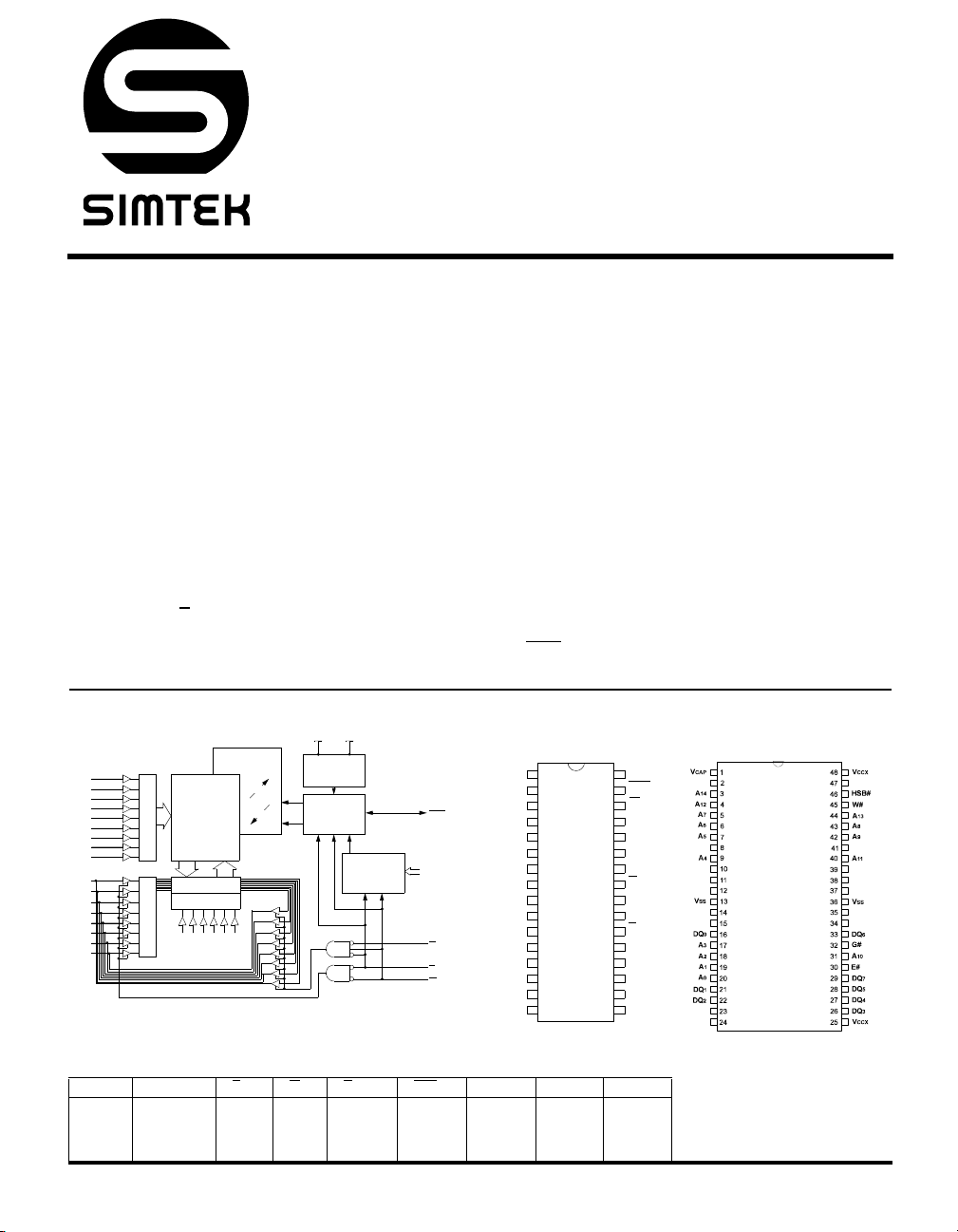
BLOCK DIAGRAM
V
CCXVCAP
Quantum Trap
STATIC RAM
ARRAY
512 x 512
COLUMN I/O
COLUMN DEC
A0 A1 A2 A3 A4 A
512 x 512
STORE
RECALL
10
A
5
A
6
A
7
A
8
A
9
A
11
A
12
A
13
A
14
DQ
0
DQ
1
DQ
2
DQ
3
DQ
4
DQ
5
DQ
6
DQ
7
ROW DECODER
INPUT BUFFERS
POWER
CONTROL
STORE/
RECALL
CONTROL
SOFTWARE
DETECT
A0 - A
HSB
G
E
W
DESCRIPTION
The Simtek STK14C88-3 is a fast static RAM with a
nonvolatile element incorporated in each static
memory cell. The
SRAM can be read and written an
unlimited number of times, while independent, nonvolatile data resides in nonvolatile elements. Data
transfers from the
STORE operation) can take place automatically
(the
SRAM to the nonvolatile elements
on power down. A 68µF or larger capacitor tied from
V
to ground guarantees the STORE operation,
CAP
regardless of power-down slew rate or loss of power
from “hot swapping”. Transfers from the nonvolatile
elements to the
SRAM (the RECALL operation) take
place automatically on restoration of power. Initia-
STORE and RECALL cycles can also be soft-
tion of
ware controlled by entering specific read
sequences. A hardware
STORE may be initiated with
the HSB pin.
PIN CONFIGURATIONS
V
V
1
CAP
A
2
14
A
3
12
A
4
7
A
5
6
A
6
5
A
7
DQ
DQ
DQ
V
NC
4
A
8
3
9
A
10
2
A
11
1
A
12
0
13
0
14
1
15
2
16
SS
13
32
CCX
HSB
31
30
W
29
A
13
28
A
8
A
27
9
A
26
11
25
G
24
NC
A
23
10
E
22
DQ
21
7
20
DQ
6
19
DQ
5
18
DQ
4
DQ
17
3
PIN NAMES
A0 - A14DQ0 -DQ7E W G HSB V
Address
Inputs
Data In/Out Chip
Enable
Write
Enable
Output
Enable
Hardware
Store
Busy (I/O)
CCX
Power
(+ 3.3V)
32 - DIP
32 - SOIC
V
CAP
Capacitor Ground
V
SS
48 - SSOP
(not to scale)
November 2003 1 Document Control # ML0015 rev 0.3
STK14C88-3
ABSOLUTE MAXIMUM RATINGS
Voltage on Input Relative to Ground . . . . . . . . . . . . . –0.5V to 4.5V
Voltage on Input Relative to V
Voltage on DQ
Temperature under Bias. . . . . . . . . . . . . . . . . . . . . .–55°C to 125°C
or HSB . . . . . . . . . . . . . . . . –0.5V to (VCC + 0.5V)
0-7
Storage Temperature . . . . . . . . . . . . . . . . . . . . . . . .–65°C to 150°C
Power Dissipation . . . . . . . . . . . . . . . . . . . . . . . . . . . . . . . . . . . 1W
. . . . . . . . . . –0.6V to (VCC + 0.5V)
SS
a
Note a: Stresses greater than those listed under “Absolute Maximum
Ratings” may cause permanent damage to the device. This is a
stress rating only, and functional operation of the device at conditions above those indicated in the operational sections of this
specification is not implied. Exposure to absolute maximum rating conditions for extended periods may affect reliability.
DC Output Current (1 output at a time, 1s duration) . . . . . . . 15mA
DC CHARACTERISTICS (VCC = 3.0V-3.6V)
SYMBOL PARAMETER
b
I
CC
I
CC
I
CC
I
CC
I
SB
I
SB
I
ILK
I
OLK
V
V
V
V
V
T
Note b: I
Note c: I
Note d: E
Note e: V
Average VCC Current 50
1
c
Average VCC Current during STORE 3 3 mA All Inputs Don’t Care, VCC = max
2
b
Average V
3
5V, 25°C, Typical
c
Average V
4
AutoStore™ Cycle
d
Average V
1
(Standby, Cycling TTL Input Levels)
d
V
CC
2
(Standby, Stable CMOS Input Levels)
Current at t
CC
Current during
CAP
Current
CC
Standby Current
Input Leakage Current
Off-State Output Leakage Current
Input Logic “1” Voltage 2.2 VCC + .5 2.2 VCC + .5 V All Inputs
IH
Input Logic “0” Voltage VSS – .5 0.8 VSS – .5 0.8 V All Inputs
IL
Output Logic “1” Voltage 2.4 2.4 V I
OH
Output Logic “0” Voltage 0.4 0.4 V I
OL
Logic “0” Voltage on HSB Output 0.4 0.4 V I
BL
Operating Temperature 0 70 – 40 85 °C
A
and I
CC
CC
≥ VIH will not produce standby current levels until any nonvolatile cycle in progress has timed out.
CC
are dependent on output loading and cycle rate. The specified values are obtained with outputs unloaded.
CC
1
3
and I
are the average currents required for the duration of the respective STORE cycles (t
CC
2
4
reference levels throughout this datasheet refer to V
AVAV
= 200ns
COMMERCIAL INDUSTRIAL
MIN MAX MIN MAX
52
42
37
44
39
99mA
22mA
18
16
15
19
17
16
11mA
±1 ±1 µA
±1 ±1 µA
.
CCX
UNITS NOTES
mA
t
= 35ns
mA
mA
AVAV
t
= 45ns
AVAV
t
= 55ns
AVAV
W ≥ (V
– 0.2V)
CC
All Others Cycling, CMOS Levels
All Inputs Don’t Care
mA
t
= 35ns, E ≥ V
mA
mA
AVAV
t
= 45ns, E ≥ V
AVAV
t
= 55ns, E ≥ V
AVAV
IH
IH
IH
E ≥ (VCC – 0.2V)
All Others VIN ≤ 0.2V or ≥ (VCC – 0.2V)
V
= max
CC
STORE
VIN = VSS to V
V
CC
V
IN
OUT
OUT
OUT
).
CC
= max
= VSS to VCC, E or G ≥ VIH
= – 4mA except HSB
= 8mA except HSB
= 3mA
e
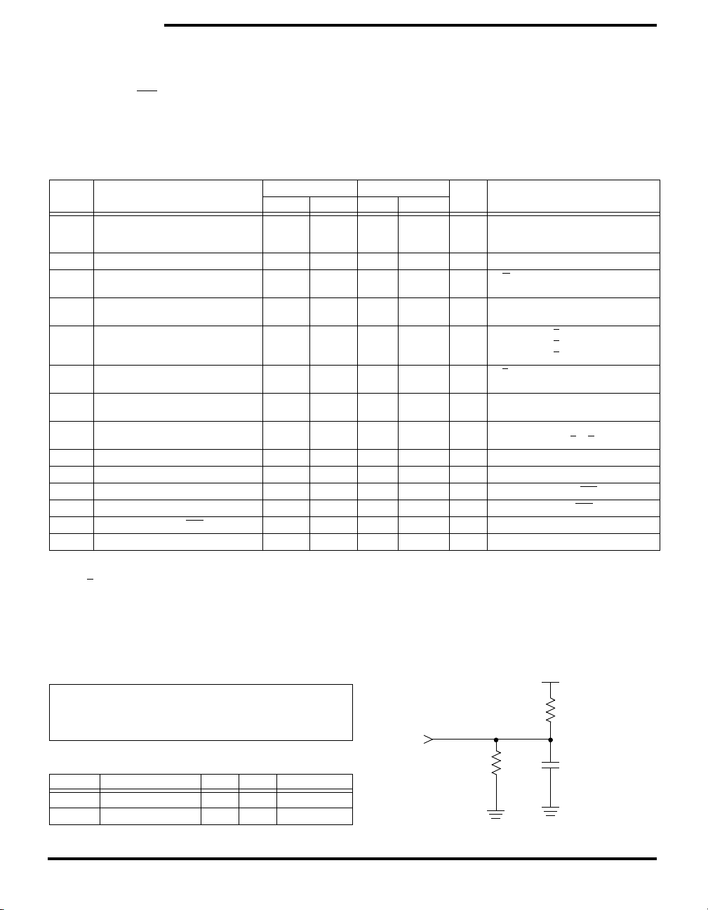
AC TEST CONDITIONS
3.3V
Input Pulse Levels . . . . . . . . . . . . . . . . . . . . . . . . . . . . . . .0V to 3V
Input Rise and Fall Times. . . . . . . . . . . . . . . . . . . . . . . . . . . . . . . . ≤ 5ns
Input and Output Timing Reference Levels . . . . . . . . . . . . . . . 1.5V
Output Load . . . . . . . . . . . . . . . . . . . . . . . . . . . . . . . . See Figure 1
f
CAPACITANCE
(TA = 25°C, f = 1.0MHz)
SYMBOL PARAMETER MAX UNITS CONDITIONS
C
IN
C
OUT
Input Capacitance 5 pF ∆V = 0 to 3V
Output Capacitance 7 pF ∆V = 0 to 3V
Note f: These parameters are guaranteed but not tested.
OUTPUT
351 Ohms
Figure 1: AC Output Loading
317 Ohms
30 pF
INCLUDING
SCOPE AND
FIXTURE
November 2003 2 Document Control # ML0015 rev 0.3
STK14C88-3
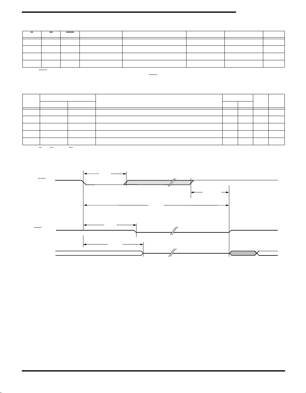
SRAM READ CYCLES #1 & #2 (VCC = 3.0V-3.6V)
NO.
1t
2t
3t
4t
5t
6t
7t
8t
9t
10 t
11 t
Note g: W and HSB must be high during SRAM READ cycles.
Note h: I/O state asumes E
Note i: Measured ± 200mV from steady state output voltage.
SYMBOLS
#1, #2 Alt. MIN MAX MIN MAX MIN MAX
ELQV
AVAV
AVQ V
GLQV
AXQX
ELQX
EHQZ
GLQX
GHQZ
ELICCH
EHICCL
t
g
t
h
t
t
h
t
t
i
t
t
i
t
f
t
f
t
Chip Enable Access Time 35 45 55 ns
ACS
Read Cycle Time 35 45 55 ns
RC
Address Access Time 35 45 55 ns
AA
Output Enable to Data Valid 15 20 25 ns
OE
Output Hold after Address Change 5 5 5 ns
OH
Chip Enable to Output Active 5 5 5 ns
LZ
Chip Disable to Output Inactive 13 15 20 ns
HZ
Output Enable to Output Active 0 0 0 ns
OLZ
Output Disable to Output Inactive 13 15 20 ns
OHZ
Chip Enable to Power Active 0 0 0 ns
PA
Chip Disable to Power Standby 35 45 55 ns
PS
and G < V
and W > VIH; device is continuously selected.
IL
PARAMETER
SRAM READ CYCLE #1: Address Controlledg,
2
t
t
AVQ V
AVAV
3
ADDRESS
DQ (DATA OUT)
t
AXQX
5
STK14C88-3-35 STK14C88-3-45 STK14C88-3-55
h
DATA VALID
UNITS
e
t
GLQV
g
2
t
AVAV
1
t
ELQV
4
ACTIVE
t
DATA VALID
9
GHQZ
t
EHQZ
t
7
11
EHICCL
SRAM READ CYCLE #2: E Controlled
ADDRESS
STANDBY
t
ELQX
10
t
ELICCH
6
t
GLQX
8
DQ (DATA OUT)
I
E
G
CC
November 2003 3 Document Control # ML0015 rev 0.3
STK14C88-3
SRAM WRITE CYCLES #1 & #2 (VCC = 3.0V-3.6V)
NO.
12 t
13 t
14 t
15 t
16 t
17 t
18 t
19 t
20 t
21 t
Note j: If W is low when E goes low, the outputs remain in the high-impedance state.
Note k: E
Note l: HSB
SRAM WRITE CYCLE #1: W Controlled
ADDRESS
SYMBOLS
#1 #2 Alt. MIN MAX MIN MAX MIN MAX
AVAV
WLWH
ELWH
DVWH
WHDX
AVW H
AVW L
WHAX
WLQZ
WHQX
t
AVAV
t
WLEH
t
ELEH
t
DVEH
t
EHDX
t
AVE H
t
AVE L
t
EHAX
i, j
or W must be ≥ V
must be high during SRAM WRITE cycles.
t
Write Cycle Time 35 45 55 ns
WC
t
Write Pulse Width 25 30 40 ns
WP
t
Chip Enable to End of Write 25 30 40 ns
CW
t
Data Set-up to End of Write 12 15 25 ns
DW
t
Data Hold after End of Write 0 0 0 ns
DH
t
Address Set-up to End of Write 25 30 40 ns
AW
t
Address Set-up to Start of Write 0 0 0 ns
AS
t
Address Hold after End of Write 0 0 0 ns
WR
t
Write Enable to Output Disable 13 15 20 ns
WZ
t
Output Active after End of Write 5 5 5 ns
OW
during address transitions.
IH
PARAMETER
k, l
12
t
AVAV
14
t
ELWH
E
17
t
t
WLQZ
AVW H
13
t
WLWH
20
DATA IN
DATA IN
DATA OUT
18
t
AVWL
W
PREVIOUS DATA
STK14C88-3-35 STK14C88-3-45 STK14C88-3-55
19
t
WHAX
15
t
DVWH
DATA VALID
HIGH IMPEDANCE
16
t
WHDX
21
t
WHQX
UNITS
e
SRAM WRITE CYCLE #2: E Controlled
ADDRESS
t
AVEL
18
k, l
t
ELEH
12
t
AVAV
14
t
EHAX
19
E
17
t
AVE H
W
DATA IN
DATA OUT
13
t
WLEH
HIGH IMPEDANCE
t
DVEH
15
DATA VALID
16
t
EHDX
November 2003 4 Document Control # ML0015 rev 0.3
STK14C88-3
HARDWARE MODE SELECTION
E W HSB A13 - A0 (hex) MODE I/O POWER NOTES
H X H X Not Selected Output High Z Standby
L H H X Read SRAM Output Data Active t
L L H X Write SRAM Input Data Active
X X L X Nonvolatile STORE Output High Z l
Note m: HSB STORE operation occurs only if an SRAM WRITE has been done since the last nonvolatile cycle. After the STORE (if any) completes,
the part will go into standby mode, inhibiting all operations until HSB
rises.
CC
2
HARDWARE STORE CYCLE (VCC = 3.0V-3.6V)
NO.
22 t
23 t
24 t
25 t
26 t
Note n: E and G low and W high for output behavior.
Note o: t
RECOVER
SYMBOLS
Standard Alternate MIN MAX
STORE
DELAY
RECOVER
HLHX
HLBL
t
HLHZ
t
HLQZ
t
HHQX
is only applicable after t
STORE Cycle Duration 10 ms i, n
Time Allowed to Complete SRAM Cycle 1 µsi, n
Hardware STORE High to Inhibit Off 700 ns n, o
Hardware STORE Pulse Width 15 ns
Hardware STORE Low to STORE Busy 300 ns
is complete.
STORE
PARAMETER
STK14C88-3
HARDWARE STORE CYCLE
25
t
HSB (IN)
HLHX
22
t
STORE
24
t
RECOVER
m
UNITS NOTES
e
26
t
DATA VALID
HLBL
t
23
DELAY
HIGH IMPEDANCE
DATA VALID
HSB (OUT)
DQ (DATA OUT)
HIGH IMPEDANCE
November 2003 5 Document Control # ML0015 rev 0.3

STK14C88-3
AutoStore™/POWER-UP RECALL (VCC = 3.0V-3.6V)
NO.
27 t
28 t
29 t
30 t
31 V
32 V
Note p: t
RESTORE
Note q: HSB
SYMBOLS
Standard Alternate MIN MAX
RESTORE
STORE
VSBL
DELAY
SWITCH
RESET
starts from the time VCC rises above V
is asserted low for 1µs when V
t
t
HLHZ
BLQZ
will be released and no STORE will take place.
PARAMETER
Power-up RECALL Duration 550 µsp
STORE Cycle Duration 10 ms n, q
Low Voltage Trigger (V
Time Allowed to Complete SRAM Cycle 1 µsn
Low Voltage Trigger Level 2.7 2.95 V
Low Voltage Reset Level 2.4 V
SWITCH
drops through V
CAP
) to HSB Low 300 ns l
SWITCH
.
. If an SRAM WRITE has not taken place since the last nonvolatile cycle, HSB
SWITCH
STK14C88-3
UNITS NOTES
AutoStore™/POWER-UP RECALL
V
CC
31
V
SWITCH
32
V
RESET
AutoStore™
e
POWER-UP RECALL
HSB
DQ (DATA OUT)
W
27
t
RESTORE
POWER-UP
RECALL
BROWN OUT
NO STORE
29
t
VSBL
30
t
DELAY
BROWN OUT
AutoStore™
28
t
STORE
BROWN OUT
AutoStore™
(NO SRAM WRITES)
NO RECALL
(V
DID NOT GO
CC
BELOW V
RESET
)
NO RECALL
(V
DID NOT GO
CC
BELOW V
RESET
RECALL WHEN
V
RETURNS
CC
)
ABOVE V
SWITCH
November 2003 6 Document Control # ML0015 rev 0.3

STK14C88-3
SOFTWARE STORE/RECALL MODE SELECTION
E W A13 - A0 (hex) MODE I/O POWER NOTES
0E38
31C7
LH
LH
03E0
3C1F
303F
0FC0
0E38
31C7
03E0
3C1F
303F
0C63
SOFTWARE-CONTROLLED STORE/RECALL CYCLE
NO.
33 t
34 t
35 t
36 t
37 t
Note r: The six consecutive addresses must be in the order listed. W must be high during all six consecutive cycles to enable a nonvolatile cycle.
Note s: While there are 15 addresses on the STK14C88-3, only the lower 14 are used to control software modes.
Note t: I/O state assumes G
Note u: The software sequence is clocked with E
Note v: The six consecutive addresses must be in the order listed in the Hardware Mode Selection Table: (0E38, 31C7, 03E0, 3C1F, 303F, 0FC0) for
SYMBOLS
Standard Alternate MIN MAX MIN MAX MIN MAX
AVAV
AVE L
ELEH
ELAX
RECALL
t
RC
t
AS
t
CW
STORE/RECALL Initiation Cycle Time 35 45 55 ns n
Address Set-up Time 0 0 0 ns u
Clock Pulse Width 25 30 45 ns u
Address Hold Time 20 20 20 ns u
RECALL Duration 20 20 20 µs
PARAMETER
< VIL. Activation of nonvolatile cycles does not depend on state of G.
a STORE cycle or (0E38, 31C7, 03E0, 3C1F, 303F, 0C63) for a RECALL cycle. W
SOFTWARE STORE/RECALL CYCLE: E CONTROLLED
33
t
ADDRESS
AVAV
Read SRAM
Read SRAM
Read SRAM
Read SRAM
Read SRAM
Nonvolatile STORE
Read SRAM
Read SRAM
Read SRAM
Read SRAM
Read SRAM
Nonvolatile RECALL
controlled READs.
Output Data
Output Data
Output Data
Output Data
Output Data
Output High Z
Output Data
Output Data
Output Data
Output Data
Output Data
Output High Z
v
STK14C88-3-25 STK14C88-3-35 STK14C88-3-45
Active
l
CC
Active
(VCC = 3.0V-3.6V)
must be high during all six consecutive cycles.
v
33
t
AVAV
ADDRESS #6ADDRESS #1
r, s, t
2
r, s, t
UNITS NOTES
e
DQ (DATA
34
t
E
AVEL
35
t
ELEH
36
t
ELAX
DATA VALID
DATA VALID
DATA VALID
28 37
t
/ t
STORE
HIGH IMPEDANCE
RECALL
November 2003 7 Document Control # ML0015 rev 0.3

STK14C88-3
DEVICE OPERATION
The STK14C88-3 has two separate modes of operation:
SRAM mode and nonvolatile mode. In SRAM
mode, the memory operates as a standard fast
static RAM. In nonvolatile mode, data is transferred
from SRAM to nonvolatile elements (the STORE
operation) or from nonvolatile elements to SRAM
(the RECALL operation). In this mode SRAM functions are disabled.
NOISE CONSIDERATIONS
The STK14C88-3 is a high-speed memory and so
must have a high-frequency bypass capacitor of
approximately 0.1µF connected between V
CAP
and
VSS, using leads and traces that are as short as possible. As with all high-speed CMOS ICs, normal care-
ful routing of power, ground and signals will help
prevent noise problems.
SRAM READ
The STK14C88-3 performs a READ cycle whenever
E and G are low and W and HSB are high. The
address specified on pins A
determines which of
0-14
the 32,768 data bytes will be accessed. When the
READ is initiated by an address transition, the out-
puts will be valid after a delay of t
#1). If the
be valid at t
READ is initiated by E or G, the outputs will
ELQV
or at t
, whichever is later (READ
GLQV
(READ cycle
AVQ V
cycle #2). The data outputs will repeatedly respond
to address changes within the t
access time with-
AVQ V
out the need for transitions on any control input pins,
and will remain valid until another address change or
or G is brought high, or W or HSB is brought
until E
low.
SRAM WRITE
A WRITE cycle is performed whenever E and W are
low and HSB is high. The address inputs must be
stable prior to entering the
remain stable until either E
end of the cycle. The data on the common I/O pins
DQ
will be written into the memory if it is valid t
0-7
before the end of a W controlled WRITE or t
before the end of an E controlled WRITE.
It is recommended that G
entire
WRITE cycle to avoid data bus contention on
common I/O lines. If G
will turn off the output buffers t
WRITE cycle and must
or W goes high at the
DVWH
DVEH
be kept high during the
is left low, internal circuitry
after W goes low.
WLQZ
POWER-UP RECALL
During power up, or after any low-power condition
(V
< V
CAP
latched. When V
voltage of V
be initiated and will take t
If the STK14C88-3 is in a
power-up
), an internal RECALL request will be
RESET
SWITCH
RECALL, the SRAM data will be corrupted.
once again exceeds the sense
CAP
, a RECALL cycle will automatically
to complete.
RESTORE
WRITE state at the end of
To help avoid this situation, a 10K Ohm resistor
should be connected either between W
V
or between E and system VCC.
CC
and system
SOFTWARE NONVOLATILE STORE
The STK14C88-3 software STORE cycle is initiated
by executing sequential E controlled READ cycles
from six specific address locations. During the
STORE cycle an erase of the previous nonvolatile
data is first performed, followed by a program of the
nonvolatile elements. The program operation copies
SRAM data into nonvolatile memory. Once a
the
STORE cycle is initiated, further input and output are
disabled until the cycle is completed.
Because a sequence of READs from specific
addresses is used for
tant that no other READ or WRITE accesses intervene in the sequence, or the sequence will be
aborted and no
STORE or RECALL will take place.
To initiate the software
READ sequence must be performed:
1. Read address 0E38 (hex) Valid READ
2. Read address 31C7 (hex) Valid READ
3. Read address 03E0 (hex) Valid READ
4. Read address 3C1F (hex) Valid READ
5. Read address 303F (hex) Valid READ
6. Read address 0FC0 (hex) Initiate STORE cycle
The software sequence must be clocked with E con-
READs.
trolled
Once the sixth address in the sequence has been
entered, the STORE cycle will commence and the
chip will be disabled. It is important that
and not WRITE cycles be used in the sequence,
although it is not necessary that G
sequence to be valid. After the t
been fulfilled, the SRAM will again be activated for
READ and WRITE operation.
STORE initiation, it is impor-
STORE cycle, the following
READ cycles
be low for the
cycle time has
STORE
November 2003 8 Document Control # ML0015 rev 0.3

STK14C88-3
SOFTWARE NONVOLATILE RECALL
A software RECALL cycle is initiated with a sequence
of READ operations in a manner similar to the soft-
STORE initiation. To initiate the RECALL cycle,
ware
the following sequence of E controlled READ operations must be performed:
1. Read address 0E38 (hex) Valid READ
2. Read address 31C7 (hex) Valid READ
3. Read address 03E0 (hex) Valid READ
4. Read address 3C1F (hex) Valid READ
5. Read address 303F (hex) Valid READ
6. Read address 0C63 (hex) Initiate RECALL cycle
Internally, RECALL is a two-step procedure. First, the
SRAM data is cleared, and second, the nonvolatile
information is transferred into the SRAM cells. After
the t
ready for
cycle time the SRAM will once again be
RECALL
READ and WRITE operations. The RECALL
operation in no way alters the data in the nonvolatile
elements. The nonvolatile data can be recalled an
unlimited number of times.
AutoStore™ OPERATION
During normal AutoStore™ operation, the
STK14C88-3 will draw current from V
capacitor connected to the V
CAP
charge will be used by the chip to perform a single
STORE operation. After power up, when the voltage
on the V
automatically disconnect the V
initiate a
pin drops below V
CAP
STORE operation.
SWITCH
CAP
Figure 2 shows the proper connection of capacitors
for automatic store operation. A charge storage
capacitor having a capacity of between 68µF and
220µF (± 20%) rated at 4.7V should be provided.
In order to prevent unneeded
STORE operations,
automatic STOREs as well as those initiated by
externally driving HSB
least one
most recent
initiated
whether a
WRITE operation has taken place since the
STORE or RECALL cycle. Software-
STORE cycles are performed regardless of
WRITE operation has taken place. An
low, will be ignored unless at
optional pull-up resistor is shown connected to HSB
This can be used to signal the system that the
AutoStore™ cycle is in progress.
to charge a
CCX
pin. This stored
, the part will
pin from V
CCX
and
10kΩ∗
1
32
31
30
+
0.1µF
68µF
Bypass
6v, ±20%
16
17
*If HSB is not used, it should be left unconnected.
Figure 2: AutoStore™ Mode
10kΩ
If the power supply drops faster than 20 µs/volt
before V
reaches V
CCX
should be inserted between V
, then a 1 ohm resistor
SWITCH
and the system
CCX
supply to avoid a momentary excess of current
between Vccx and Vcap.
HSB OPERATION
The STK14C88-3 provides the HSB pin for controlling and acknowledging the
HSB pin can be used to request a hardware STORE
cycle. When the HSB pin is driven low, the
STK14C88-3 will conditionally initiate a
ation after t
; an actual STORE cycle will only
DELAY
begin if a WRITE to the SRAM took place since the
STORE or RECALL cycle. The HSB pin also acts
last
as an open drain driver that is internally driven low
to indicate a busy condition while the
ated by any means) is in progress.
SRAM READ and WRITE operations that are in
progress when HSB
is driven low by any means are
given time to complete before the STORE operation
is initiated. After HSB
will continue
multiple
WRITE is in progress when HSB is pulled low it will
.
be allowed a time, t
SRAM WRITE cycles requested after HSB goes low
SRAM operations for t
SRAM READ operations may take place. If a
DELAY
will be inhibited until HSB
The HSB
pin can be used to synchronize multiple
STK14C88-3s while using a single larger capacitor.
STORE operations. The
STORE oper-
STORE (initi-
goes low, the STK14C88-3
. During t
DELAY
, to complete. However, any
returns high.
DELAY
,
November 2003 9 Document Control # ML0015 rev 0.3

STK14C88-3
To operate in this mode the HSB pin should be connected together to the HSB
pins from the other
STK14C88-3s. An external pull-up resistor to + 3.3V
is required since HSB
down. The V
CAP
acts as an open drain pull
pins from the other STK14C88-3
parts can be tied together and share a single capacitor. The capacitor size must be scaled by the number of devices connected to it. When any one of the
STK14C88-3s detects a power loss and asserts
, the common HSB pin will cause all parts to
HSB
request a
STORE cycle (a STORE will take place in
those STK14C88-3s that have been written since
the last nonvolatile cycle).
During any
STORE operation, regardless of how it
was initiated, the STK14C88-3 will continue to drive
the HSB pin low, releasing it only when the STORE is
complete. Upon completion of the
STORE operation
the STK14C88-3 will remain disabled until the HSB
pin returns high.
If HSB is not used, it should be left unconnected.
HARDWARE PROTECT
The STK14C88-3 offers hardware protection against
inadvertent STORE operation and SRAM WRITEs during low-voltage conditions. When V
externally initiated
WRITE
s will be inhibited.
STORE operations and SRAM
CAP
< V
SWITCH
, all
LOW AVERAGE ACTIVE POWER
The STK14C88-3 draws significantly less current
when it is cycled at times longer than 55ns. Figure 3
shows the relationship between ICC and READ cycle
time. Worst-case current consumption is shown for
CMOS and TTL input levels (commercial tem-
both
perature range, VCC = 3.6V, 100% duty cycle on chip
enable). Figure 4 shows the same relationship for
WRITE cycles. If the chip enable duty cycle is less
than 100%, only standby current is drawn when the
chip is disabled. The overall average current drawn
by the STK14C88-3 depends on the following items:
CMOS vs. TTL input levels; 2) the duty cycle of
1)
chip enable; 3) the overall cycle rate for accesses;
4) the ratio of
temperature; 6) the V
READs to WRITEs; 5) the operating
level; and 7) I/O loading.
cc
50
40
30
20
10
Average Active Current (mA)Average Active Current (mA)
0
50 100 150 200
Cycle Time (ns)
Figure 3: Icc (max) Reads
50
40
30
20
10
Average Active Current (mA)
0
50 100 150 200
Cycle Time (ns)
Figure 4: I
cc
TTL
CMOS
TTL
CMOS
(max) Writes
November 2003 10 Document Control # ML0015 rev 0.3

ORDERING INFORMATION
STK14C88-3 N F 45 I
STK14C88-3
Temperature Range
Blank = Commercial (0 to 70°C)
I = Industrial (-40 to 85°C)
Access Time
35 = 35ns
45 = 45ns
55 = 55ns
Lead Finish
Blank = 85%Sn/15%Pb
F = 100% Sn (Matte Tin)
Package
N = Plastic 32-pin 300 mil SOIC
W = Plastic 32-pin 600 mil DIP
R = Plastic 48-pin 300 mil SSOP
November 2003 11 Document Control # ML0015 rev 0.3

STK14C88-3
Document Revision History
Revision
0.0
0.1
0.2
0.3
Date Summary
January 2003
February 2003 Added 48 SSOP package
September 2003 Added lead-free lead finish
November 2003 Modified pin assignments on 48 SSOP package
Added 35 nsec device; added HSB
extreme power-off slew rate
operation; current limiting resistor added to Vccx for
November 2003 12 Document Control # ML0015 rev 0.3

STK14C88-3
November 2003 13 Document Control # ML0015 rev 0.3

WWW.ALLDATASHEET.COM
Copyright © Each Manufacturing Company.
All Datasheets cannot be modified without permission.
This datasheet has been download from :
www.AllDataSheet.com
100% Free DataSheet Search Site.
Free Download.
No Register.
Fast Search System.
www.AllDataSheet.com
 Loading...