

SIMTEK STK12C68-C35IM, STK12C68-C25IM, STK12C68-L45IM, STK12C68-L25IM, STK12C68-L35IM Datasheet
...
STK12C68-IM
A
A
A
A
A
A
A
A
A
A
A
A
DQ
DQ
DQDQDQ
DQ
DQ
G
A
E
DQ
Vss
V
W
HSB
7
12
6
5
4
3
2
1
0
0
1
8
9
11
10
7
6
234
5
TOP VIEW
4
5
6
7
8
9
10
11
12
32128 27
26
25
24
23
22
21
20
19
18
1716151413
V
CAP
CCX
STK12C68-IM
CMOS nvSRAM
Industrial Temperature/Military Screen
FEATURES
• Industrial Temperature with Military Screening
• 25, 35 and 45ns Access Times
• 15 mA I
• Automatic
• Hardware or Software initiated
EEPROM
• Automatic
• 100,000
• 10 year data retention in EEPROM
• Automatic
• Software initiated
• Unlimited
• Single 5V±10% Operation
• Commercial and Industrial Temperatures
• Available in multiple standard packages
at 200ns Access Speed
CC
STORE
STORE
STORE
RECALL
RECALL
to EEPROM on Power Down
Timing
cycles to EEPROM
on Power Up
RECALL
from EEPROM
cycles from EEPROM
STORE
to
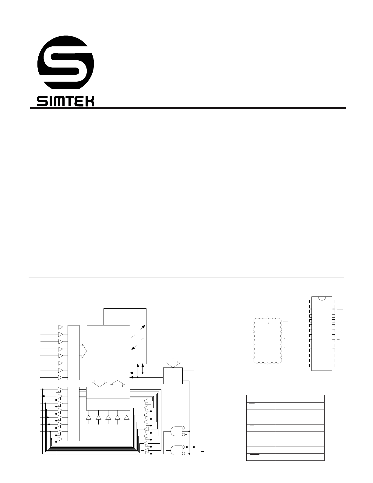
8K x 8
AutoStore™
Nonvolatile Static RAM
DESCRIPTION
The Simtek STK12C68-IM is a fast static RAM (25, 35
and 45ns), with a nonvolatile EEPROM element incorporated in each static memory cell. The SRAM can be
read and written an unlimited number of times, while
independent nonvolatile data resides in EEPROM. Data
transfers from the SRAM to the EEPROM (the
operation) take place automatically upon power down
using charge stored in an external 100 µF capacitor.
Transfers from the EEPROM to the SRAM (the
operation) take place automatically on power up. Software sequences may also be used to initiate both
STORE
and
RECALL
operations. A
STORE
initiated via a single pin.
The STK12C68-IM is available in the following
packages: a 28-pin 300 mil ceramic DIP and a 28-pad
LCC. MIL-STD-883 and Standard Military Drawing
(SMD 5962-94599) devices are also available.
STORE
RECALL
can also be
LOGIC BLOCK DIAGRAM
A
3
A
4
A
5
A
6
A
7
A
8
A
9
A
12
DQ
0
DQ
1
DQ
2
DQ
3
DQ
4
DQ
5
DQ
6
DQ
7
ROW DECODER
INPUT BUFFERS
EEPROM ARRAY
256 x 256
STORE
STATIC RAM
ARRAY
256 x 256
COLUMN I/O
COLUMN DECODER
AAAAA
1210
011
RECALL
AA
0
12
STORE/
RECALL
CONTROL
41
HSB
PIN CONFIGURATIONS
1
V
CAP
2
A
12
3
A
7
4
A
6
5
A
5
6
A
4
7
A
3
8
A
2
9
A
1
10
A
0
11
DQ
0
12
DQ
1
13
DQ
2
14
V
SS
V
28
CCX
W
27
26
HSB
25
A
8
24
A
9
23
A
11
22
G
21
A
10
20
E
19
DQ
7
18
DQ
6
17
DQ
5
16
DQ
4
15
DQ
3
28 - LCC 28 - 300 CDIP
PIN NAMES
A0 - A
W Write Enable
DQ0 - DQ7Data In/Out
E Chip Enable
G
E
W
G Output Enable
V
CCX
V
SS
V
CAP
HSB Hardware Store/Busy
12
Address Inputs
Power (+5V)
Ground
Capacitor

STK12C68-IM
ABSOLUTE MAXIMUM RATINGS
Voltage on typical input relative to VSS. . . . . . . . . . . . . –0.6V to 7.0V
Voltage on DQ
Temperature under bias . . . . . . . . . . . . . . . . . . . . . . –55°C to 125°C
Storage temperature. . . . . . . . . . . . . . . . . . . . . . . . . –65°C to 150°C
Power dissipation. . . . . . . . . . . . . . . . . . . . . . . . . . . . . . . . . . . . . .1W
DC output current . . . . . . . . . . . . . . . . . . . . . . . . . . . . . . . . . . .15mA
and G. . . . . . . . . . . . . . . . . . .–0.5V to (VCC+0.5V)
0-7
a
Note a: Stresses greater than those listed under "Absolute Maximum
Ratings" may cause permanent damage to the device. This is a stress
rating only, and functional operation of the device at conditions above
those indicated in the operational sections of this specification is not
implied. Exposure to absolute maximum rating conditions for extended
periods may affect reliability.
(One output at a time, one second duration)
DC CHARACTERISTICS (VCC = 5.0V ± 10%)
SYMBOL PARAMETER UNITS NOTES
b
I
I
I
I
I
I
I
I
V
V
V
V
T
CC
CC
CC
CC
SB
SB
ILK
OLK
A
Average VCC Current 95 mA t
1
Average VCC Current During
2
b
Average VCC Current 15 mA E ≤ 0.2V, W ≥ (VCC – 0.2V)
IH
IL
OH
OL
3
4
c
1
c
2
3
= 200ns others ≤ 0.2V or ≥ (VCC – 0.2V)
at t
AVAV
Average V
Average VCC Current 39 mA t
(Standby, Cycling TTL Input Levels) 35 mA t
Average VCC Current 3 mA E ≥ (VCC – 0.2V)
(Standby, Stable CMOS Input Levels) all others V
Input Leakage Current (Any Input) ±1 µAVCC = max
Off State Output Leakage Current ±5 µAVCC = max
Input Logic "1" Voltage 2.2 VCC+.5 V All Inputs
Input Logic "0" Voltage VSS–.5 0.8 V All Inputs
Output Logic "1" Voltage 2.4 V I
Output Logic "0" Voltage 0.4 V I
Operating Temperature -40 85 °C
current during AutoStore™ Cycle 4 mA All inputs ≤ 0.2V or ≥ (VCC - 0.2V)
CC
STORE
INDUSTRIAL
MIN MAX
85 mA t
80 mA t
7 mA All inputs ≤ 0.2V or ≥ (VCC - 0.2V)
32 mA t
= 25ns
AVAV
= 35ns
AVAV
= 45ns
AVAV
= 25ns
AVAV
= 35ns
AVAV
= 45ns
AVAV
; all others cycling
E ≥ V
IH
≤ 0.2V or ≥ (VCC – 0.2V)
IN
= VSS to V
V
IN
= VSS to V
V
OUT
= –4mA except HSB
OUT
= 8mA except HSB
OUT
CC
CC
d
Note b: ICC and ICC are dependent on output loading and cycle rate. The specified values are obtained with outputs unloaded.
Note c: Bringing E ≥ VIH will not produce standby current levels until any nonvolatile cycle in progress has timed out. See MODE SELECTION table.
Note d: VCC reference levels throughout this datasheet refer to V
AC TEST CONDITIONS
3
1
if that is where the power supply connection is made, or V
CCX
CAP
if V
is connected to ground.
CCX
5.0V
Input Pulse Levels. . . . . . . . . . . . . . . . . . . . . . . . . . . . . VSS to 3V
Input Rise and Fall Times. . . . . . . . . . . . . . . . . . . . . . . . . . ≤ 5ns
Input and Output Timing Reference Levels. . . . . . . . . . . . . . 1.5V
Output Load. . . . . . . . . . . . . . . . . . . . . . . . . . . . . . . See Figure 1
CAPACITANCEe (T
SYMBOL PARAMETER MAX UNITS CONDITIONS
C
IN
C
OUT
Note e: These parameters are guaranteed but not tested.
Input Capacitance 8 pF ∆V = 0 to 3V
Output Capacitance 7 pF ∆V = 0 to 3V
=25°C, f=1.0MHz)
A
Output
255 Ohms
Figure 1: AC Output Loading
480 Ohms
30pF
INCLUDING
SCOPE
AND FIXTURE
42

SRAM MEMORY OPERATION
STK12C68-IM
READ CYCLES #1 & #2
(VCC = 5.0V ± 10%)
SYMBOLS STK12C68-25-IM STK12C68-35-IM STK12C68-45-IM
NO. PARAMETER UNITS
1t
2t
3t
4t
5t
6t
7t
8t
9t
10 t
11 t
Note c: Bringing E ≥ V
#1, #2 Alt. MIN MAX MIN MAX MIN MAX
ELQV
AVAV
AVQV
GLQV
AXQX
ELQX
EHQZ
GLQX
GHQZ
ELICCH
EHICCL
t
ACS
t
RC
g
t
AA
t
OE
t
OH
t
LZ
h
t
HZ
t
OLZ
h
t
OHZ
e
t
PA
c,e
t
PS
will not produce standby currents until any nonvolatile cycle in progress has timed out. See MODE SELECTION table.
IH
Chip Enable Access Time 25 35 45 ns
Read Cycle Time 25 35 45 ns
Address Access Time 25 35 45 ns
Output Enable to Data Valid 10 20 25 ns
Output Hold After Address Change 5 5 5 ns
Chip Enable to Output Active 5 5 5 ns
Chip Disable to Output Inactive 10 17 20 ns
Output Enable to Output Active 0 0 0 ns
Output Disable to Output Inactive 10 17 20 ns
Chip Enable to Power Active 0 0 0 ns
Chip Disable to Power Standby 25 35 45 ns
Note e: Parameter guaranteed but not tested.
Note f: For READ CYCLE #1 and #2, W is high for entire cycle.
Note g: Device is continuously selected with E low and G low.
Note h: Measured ± 200mV from steady state output voltage.
d
READ CYCLE #1
ADDRESS
DQ (Data Out)
READ CYCLE #2
ADDRESS
E
G
DQ (Data Out)
ACTIVE
I
CC
STANDBY
f,g
f
10
t
ELICCH
t
AXQX
5
t
ELQX
2
t
AVAV
3
t
AVQV
DATA VALID
2
t
AVAV
1
t
t
GLQX
8
t
GLQV
ELQV
4
t
GHQZ
DATA VALID
9
6
t
EHQZ
7
11
t
EHICCL
43

STK12C68-IM
WRITE CYCLES #1 & #2
(VCC = 5.0V ± 10%)
SYMBOLS STK12C68-25-IM STK12C68-35-IM STK12C68-45-IM
NO. PARAMETER UNITS
12 t
13 t
14 t
15 t
16 t
17 t
18 t
19 t
20 t
21 t
#1 #2 Alt. MIN MAX MIN MAX MIN MAX
AVAV
WLWH
ELWH
DVWH
WHDX
AVWH
AVWL
WHAX
WLQZ
WHQX
t
AVAV
t
WLEH
t
ELEH
t
DVEH
t
EHDX
t
AVEH
t
AVEL
t
EHAX
h,j
t
t
t
t
t
t
t
t
t
t
WC
WP
CW
DW
DH
AW
AS
WR
WZ
OW
Write Cycle Time 25 35 45 ns
Write Pulse Width 20 30 35 ns
Chip Enable to End of Write 20 30 35 ns
Data Set-up to End of Write 10 18 20 ns
Data Hold After End of Write 0 0 0 ns
Address Set-up to End of Write 20 30 35 ns
Address Set-up to Start of Write 0 0 0 ns
Address Hold After End of Write 0 0 0 ns
Write Enable to Output Disable 10 17 20 ns
Output Active After End of Write 5 5 5 ns
Note h: Measured ±200mV from steady state output voltage.
Note i: E or W must be ≥VIH during address transitions.
Note j: If W is low when E goes low, the outputs remain in the high impedance state.
WRITE CYCLE #1: W CONTROLLED
i
12
t
AVAV
ADDRESS
14
t
ELWH
19
t
WHAX
E
17
t
AVWH
20
t
WLQZ
13
t
WLWH
15
t
DVWH
DATA VALID
HIGH IMPEDANCE
16
t
WHDX
21
t
WHQX
DATA IN
DATA OUT
18
t
W
AVWL
PREVIOUS DATA
d
WRITE CYCLE #2: E CONTROLLED
ADDRESS
18
t
AVEL
E
W
DATA IN
DATA OUT
i
t
12
t
AVAV
14
t
ELEH
17
AVEH
13
t
WLEH
HIGH IMPEDANCE
44
15
t
DVEH
DATA VALID
16
t
EHDX
t
EHAX
19

STK12C68-IM
NONVOLATILE MEMORY OPERATION
MODE SELECTION
E W HSB A12 - A0(hex) MODE I/O POWER NOTES
H X H X Not Selected Output High Z Standby
L H H X Read SRAM Output Data Active l
L L H X Write SRAM Input Data Active
L H H 0000 Read SRAM Output Data Active k,l
1555 Read SRAM Output Data k,l
0AAA Read SRAM Output Data k,l
1FFF Read SRAM Output Data k,l
10F0 Read SRAM Output Data k,l
0F0F Nonvolatile
STORE
L H H 0000 Read SRAM Output Data Active k,l
1555 Read SRAM Output Data k,l
0AAA Read SRAM Output Data k,l
1FFF Read SRAM Output Data k,l
10F0 Read SRAM Output Data k,l
0F0E Nonvolatile
XXL X
RECALL
STORE
/Inhibit Output High Z I
Note k: The six consecutive addresses must be in order listed - (0000, 1555, 0AAA, 1FFF, 10F0, 0F0F) for a
0F0E) for a
RECALL
cycle. W must be high during all six consecutive cycles. See
STORE
Note l: I/O state assumes that G ≤ VIL. Activation of nonvolatile cycles does not depend on the state of G.
Note m: HSB initiated
STORE
operation actually occurs only if a WRITE has been done since last
part will go into standby mode inhibiting all operation until HSB rises.
Output High Z k
Output High Z k
/Standby m
CC2
STORE
cycle or (0000, 1555, 0AAA, 1FFF, 10F0,
cycle and
STORE
RECALL
cycle tables and diagrams for further details.
operation. After the
STORE
(if any) completes, the
HARDWARE
STORE /RECALL
SYMBOLS
NO. PARAMETER MIN MAX UNITS NOTES
22 t
23 t
24 t
25 t
26 t
RECALL
STORE
DELAY
RECOVER
ASSERT
V
SWITCH
I
HSB_OL
I
HSB_OH
t
HLHH
t
HLQZ
t
HHQX
t
HLHX
RECALL
Cycle Duration 20 µs Note o
STORE
Cycle Duration 10 ms VCC ≥ 4.5V
HSB Low to Inhibit On 1 µs
HSB High to Inhibit Off 700 ns Note e
External
STORE
Pulse Width 250 ns Note e
Low Voltage Trigger Level 4.0 4.5 V
HSB Output Low Current 3 mA HSB = VOL, Note e, n
HSB Output High Current 5 60 µA HSB = VIL, Note e, n
Note e: These parameters guaranteed but not tested.
Note n: HSB is an I/O that has a weak internal pullup; it is basically an open drain output. It is meant to allow up to 32 STK12C68-IMs to be ganged together for
simultaneous storing. Do not use HSB to pullup any external circuitry other than other STK12C68 HSB pins.
Note o: A RECALL cycle is initiated automatically at power up when VCC exceeds V
HARDWARE
V
SWITCH
V
CAP
HSB
STORE /RECALL
24
t
DELAY
SWITCH
. t
RESTORE
is measured from the point at which VCC exceeds 4.5V.
26
t
ASSERT
RECALL
STORE
SRAM
Inhibit
W
23
t
STORE
22
t
RECALL
24
t
DELAY
t
STORE
25
t
RECOVER
23
23
t
STORE
Software STOREHSB Initiated STOREPower Down STOREBrown Out RECALLPower Up RECALL
45

STK12C68-IM
SOFTWARE STORE/RECALL CYCLE
(VCC = 5.0V ± 10%)
d
NO. PARAMETER UNITS
27 t
28 t
29 t
30 t
31 t
32 t
Note p: Once the software
Std. Alt. MIN MAX MIN MAX MIN MAX
AVAV
p
ELQZ
AVELN
p,q
ELEHN
EHAXN
RESTORE
t
RC
t
AE
t
EP
t
EA
Store/Recall Initiation Cycle Time 25 35 45 ns
Chip Enable to Output Inactive 650 650 650 ns
Address Set-up to Chip Enable 0 0 0 ns
Chip Enable Pulse Width 20 25 35 ns
Chip Disable to Address Change 0 0 0 ns
Power-up Recall Duration 550 550 550 µs
STORE
or
RECALL
cycle is initiated, it completes automatically, ignoring all inputs.
Note q: Noise on the E pin may trigger multiple read cycles from the same address and abort the address sequence.
SYMBOLS STK12C68-25-IM STK12C68-35-IM STK12C68-45-IM
Note r: If the Chip Enable Pulse Width is less than t
of the low pulse, however the
STORE
or
(see READ CYCLE #2) but greater than or equal to t
ELQV
RECALL
will still be initiated.
, then the data may not be valid at the end
ELEHN
Note s: W must be HIGH when E is LOW during the address sequence in order to initiate a nonvolatile cycle. G may be either HIGH or LOW throughout.
Addresses #1 through #6 are found in the MODE SELECTION table. Address #6 determines whether the STK12C68-IM performs a
Note t: E must be used to clock in the address sequence for the Software
SOFTWARE STORE/RECALL CYCLE
28
t
AVAV
ADDRESS
DQ(Data Out)
30
t
AVELN
E
31
t
ELEHN
VALID
32
t
EHAXN
q,r,t
STORE
28
t
AVAV
ADDRESS #2
and
RECALL
cycles.
ADDRESS #6ADDRESS #1
23
t
STORE
29
t
ELQZ
VALID
22
t
RECALL
HIGH IMPEDANCE
STORE
or
RECALL
.
46

DEVICE OPERATION
STK12C68-IM
The STK12C68-IM has two separate modes of operation: SRAM mode and nonvolatile mode. In SRAM
mode, the memory operates as a standard fast static
RAM. In nonvolatile mode, data is transferred from
SRAM to EEPROM (the
EEPROM to SRAM (the
SRAM functions are disabled.
STORE
cycles may be initiated under user control via a
STORE
RECALL
operation) or from
operation). In this mode
software sequence or HSB assertion and are also
automatically initiated when the power supply voltage
level of the chip falls below V
SWITCH
.
RECALL
operations are automatically initiated upon power-up and
whenever the power supply voltage level rises above
V
SWITCH
.
RECALL
cycles may also be initiated by a
software sequence.
SRAM READ
The STK12C68-IM performs a READ cycle whenever E
and G are LOW and HSB and W are HIGH. The address
specified on pins A
determines which of the 8192
0-12
data bytes will be accessed. When the READ is initiated
by an address transition, the outputs will be valid after
a delay of t
outputs will be valid at t
. If the READ is initiated by E or G, the
AVQV
ELQV
or at t
, whichever is
GLQV
later. The data outputs will repeatedly respond to
address changes within the t
access time without
AVQV
the need for transitions on any control input pins, and
will remain valid until another address change or until
E or G is brought HIGH or W or HSB is brought LOW.
SRAM WRITE
A write cycle is performed whenever E and W are LOW
and HSB is high. The address inputs must be stable prior
to entering the WRITE cycle and must remain stable
until either E or W go HIGH at the end of the cycle. The
data on pins DQ
is valid t
or t
DVWH
before the end of an E controlled WRITE.
DVEH
It is recommended that G be kept HIGH during the entire
WRITE cycle to avoid data bus contention on the
common I/O lines. If G is left LOW, internal circuitry will
turn off the output buffers t
will be written into the memory if it
0-7
before the end of a W controlled WRITE
after W goes LOW.
WLQZ
address locations. By relying on READ cycles only, the
STK12C68-IM implements nonvolatile operation while
remaining compatible with standard 8Kx8 SRAMs.
During the
STORE
cycle, an erase of the previous
nonvolatile data is first performed, followed by a program of the nonvolatile elements. The program operation copies the SRAM data into the nonvolatile elements. Once a
STORE
cycle is initiated, further input
and output are disabled until the cycle is completed.
Because a sequence of addresses is used for
STORE
initiation, it is critical that no other read or write accesses intervene in the sequence or the sequence will
be aborted.
To initiate the
STORE
cycle the following READ se-
quence must be performed:
1. Read address 0000 (hex) Valid READ
2. Read address 1555 (hex) Valid READ
3. Read address 0AAA (hex) Valid READ
4. Read address 1FFF (hex) Valid READ
5. Read address 10F0 (hex) Valid READ
6. Read address 0F0F (hex) Initiate
STORE
Cycle
Once the sixth address in the sequence has been
entered, the
STORE
cycle will commence and the chip
will be disabled. It is important that READ cycles and
not WRITE cycles be used in the sequence, although it
is not necessary that G be LOW for the sequence to be
valid. After the t
SRAM will again be activated for READ and WRITE
cycle time has been fulfilled, the
STORE
operation.
SOFTWARE RECALL
A
RECALL
initiated with a sequence of READ operations in a
manner similar to the
RECALL
tions must be performed:
1. Read address 0000(hex) Valid READ
2. Read address 1555 (hex) Valid READ
3. Read address 0AAA (hex) Valid READ
4. Read address 1FFF (hex) Valid READ
5. Read address 10F0 (hex) Valid READ
6. Read address 0F0E (hex) Initiate
cycle of the EEPROM data into the SRAM is
STORE
initiation. To initiate the
cycle the following sequence of READ opera-
RECALL
Cycle
SOFTWARE
The STK12C68-IM software
STORE
STORE
cycle is initiated by
executing sequential READ cycles from six specific
Internally,
RECALL
is a two step procedure. First, the
SRAM data is cleared and second, the nonvolatile
information is transferred into the SRAM cells. The
RECALL
operation in no way alters the data in the
47
STK12C68-IM
EEPROM cells. The nonvolatile data can be recalled an
unlimited number of times.
AUTOMATIC RECALL
During power-up, or after any low power condition
(V
< V
CAP
voltage of V
SWITCH
SWITCH
), when V
, a
RECALL
exceeds the sense
CAP
cycle will automatically
be initiated.
If the STK12C68-IM is in a WRITE state at the end of
power-up
RECALL
, the SRAM data will be corrupted.
To help avoid this situation, a 10K Ohm resistor should
be connected between W and system VCC.
HARDWARE PROTECT
The STK12C68-IM offers hardware protection against
inadvertent
conditions. When V
initiated
STORE
STORE
operation during low voltage
CAP
< V
SWITCH,
all externally
operations will be inhibited.
HSB OPERATION
The Hardware Store Busy pin (HSB) is an open drain
circuit acting as both input and output to perform two
different functions. When driven low by the internal
chip circuitry it indicates that a
ated via any means) is in progress within the chip.
When driven low by external circuitry for longer than
t
ASSERT
operation after t
READ and WRITE operations that are in progress when
, the chip will conditionally initiate a
.
DELAY
HSB is driven low (either by internal or external circuitry) will be allowed to complete before the
operation is performed, in the following manner. After
HSB goes low, the part will continue normal SRAM
operations for t
DELAY
. During t
any address or control signal will terminate SRAM
operation and cause the
that if an SRAM write is attempted after HSB has been
forced low, the write will not occur and the
operation will begin immediately.
HARDWARE-STORE-BUSY (HSB) is a high speed,
low drive capability bi-directional control line. In order
to allow a bank of STK12C68-IMs to perform synchronized
STORE
functions, the HSB pin from a number of
chips may be connected together. Each chip contains
a small internal current source to pull HSB HIGH when
it is not being driven low. To decrease the sensitivity
of this signal to noise generated on the PC board, it
STORE
STORE
DELAY
operation (initi-
STORE
STORE
, a transition on
to commence. Note
STORE
may optionally be pulled to V
via an external
CCX
resistor with a value such that the combined load of the
resistor and all parallel chip connections does not
exceed I
HSB_OL
other pull-up to the V
at VOL. Do not connect this or any
node.
CAP
If HSB is to be connected to external circuits other than
other STK12C68-IMs, an external pull-up resistor
should be used.
During any
STORE
operation, regardless of how it was
initiated, the STK12C68-IM will continue to drive the
HSB pin low, releasing it only when the
complete. Upon completion of a
STORE
STORE
is
operation, the
part will be disabled until HSB actually goes HIGH.
AUTOMATIC
STORE
OPERATION
During normal operation, the STK12C68-IM will draw
current from V
to the V
pin. This stored charge will be used by the
CAP
chip to perform a single
up, when the voltage on the V
V
SWITCH
V
CAP
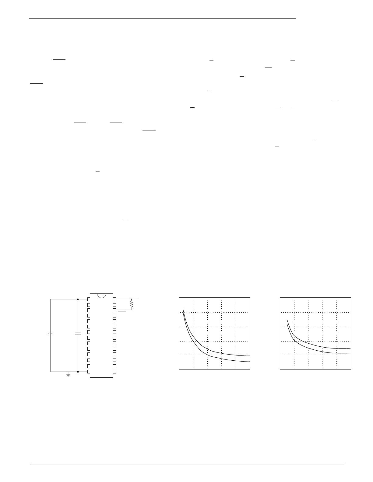
Figure 1
, the part will automatically disconnect the
pin from V
shows the proper connection of capacitors for
to charge up a capacitor connected
CCX
STORE
and initiate a
CCX
operation. After power
pin drops below
CAP
STORE
operation.
automatic store operation. The charge storage capacitor should have a capacity of at least 100µF (± 20%) at
6V. Each STK12C68-IM must have its own 100µF
capacitor. Each STK12C68-IM
must
have a high
quality, high frequency bypass capacitor of 0.1µF
connected between V
and VSS, using leads and
CAP
traces that are as short as possible.
If the
AutoStore
should be tied directly to the power supply and V
should be tied to ground. In this mode,
™ function is not required, then V
STORE
opera-
CAP
CCX
tions may be triggered through software control or the
HSB pin. In either event, V
CAP
(Pin 1)
must
always
have a proper bypass capacitor connected to it.
In order to prevent unneeded
matic
STOREs
as well as those initiated by externally
STORE
operations, auto-
driving HSB LOW will be ignored unless at least one
WRITE operation has taken place since the most recent
STORE
cycle. Note that if HSB is driven low via external
circuitry and no WRITEs have taken place, the part will
still be disabled until HSB is allowed to return HIGH.
Software initiated
STORE
cycles are performed regardless of whether or not a WRITE operation has taken
place.
48
STK12C68-IM
100
80
60
40
20
50 100 150 200
Average Active Current (ma)
0
TTL
CMOS
Cycle Time (ns)
PREVENTING AUTOMATIC STORES
The
AutoStore
™function can be disabled on the fly by
holding HSB HIGH with a driver capable of sourcing
15mA at a VOH of at least 2.2V as it will have to
overpower the internal pull-down device that drives
HSB low for 20µs at the onset of an
AutoStore
™.
When the STK12C68-IM is connected for
AutoStore
and a 100uF capacitor on V
V
SWITCH
™operation (system VCC connected to V
) and VCC crosses
CAP
CCX
on the way down, the STK12C68-IM will
attempt to pull HSB low; if HSB doesn't actually get
below VIL, the part will stop trying to pull HSB LOW and
abort the
AutoStore
™attempt.
LOW AVERAGE ACTIVE POWER
The STK12C68-IM has been designed to draw significantly less power when E is LOW (chip enabled) but the
access cycle time is longer than 55ns.
shows the relationship between ICC and access times
for READ cycles. All remaining inputs are assumed to
cycle, and current consumption is given for all inputs at
CMOS or TTL levels.
Figure 3
shows the same relationship for WRITE cycles. When E is HIGH, the chip
consumes only standby currents, and these plots do
not apply.
Figure 2
below
The cycle time used in
Figure 2
corresponds to the
length of time from the later of the last address transition or E going LOW to the earlier of E going HIGH or the
next address transition. W is assumed to be HIGH,
while the state of G does not matter. Additional current
is consumed when the address lines change state
while E is asserted. The cycle time used in
Figure 3
corresponds to the length of time from the later of W or
E going LOW to the earlier of W or E going HIGH.
The overall average current drawn by the part depends
on the following items: 1) CMOS or TTL input levels; 2)
the time during which the chip is disabled (E HIGH); 3)
the cycle time for accesses (E LOW); 4) the ratio of
reads to writes; 5) the operating temperature; 6) the
VCC level; and 7) output load.
100uF
± 20%
+
V
CAP CCX
1
0.1uF
Bypass
Schematic Diagram
V
SS
14
Figure 1
nvSRAM
V
28
26
HSB
Power
Supply
10K Ohms
(optional)
100
80
60
40
20
Average Active Current (ma)
0
50 100 150 200
Cycle Time (ns)
Figure 2
I
(Max) Reads
CC
TTL
CMOS
Figure 3
ICC (Max) Writes
Note: Typical at 25° C
49
STK12C68-IM
STK12C68 - C 35 IM
ORDERING INFORMATION
Temperature Range
IM = Industrial (-40 to +85°C) with Military Screening
Access Time
25 = 25ns
35 = 35ns
45 = 45ns
Package
C = Ceramic 28 pin 300 mil DIP with Gold Lead Finish
K = Ceramic 28 pin 300 mil DIP with Solder DIP
L = Ceramic 28 pin LCC
50
 Loading...