

SIMTEK STK11C68-C25I, STK11C68-C20, STK11C68-C25, STK11C68-S45I, STK11C68-S35I Datasheet
...
STK11C68
8K x 8 nvSRAM
QuantumTrap™ CMOS
Nonvolatile Static RAM
FEATURES
• 20ns, 25ns, 35ns and 45ns Access Times
• STORE to EEPROM Initiated by Software
• RECALL to SRAM Initiated by Software or
Power Restore
• 10mA Typical I
at 200ns Cycle Time
CC
• Unlimited READ, WRITE and RECALL Cycles
• 1,000,000 STORE Cycles to EEPROM
• 100-Year Data Retention over Full Industrial
Temperature Range
• Commercial and Industrial Temperatures
• 28-Pin DIP and SOIC Packages
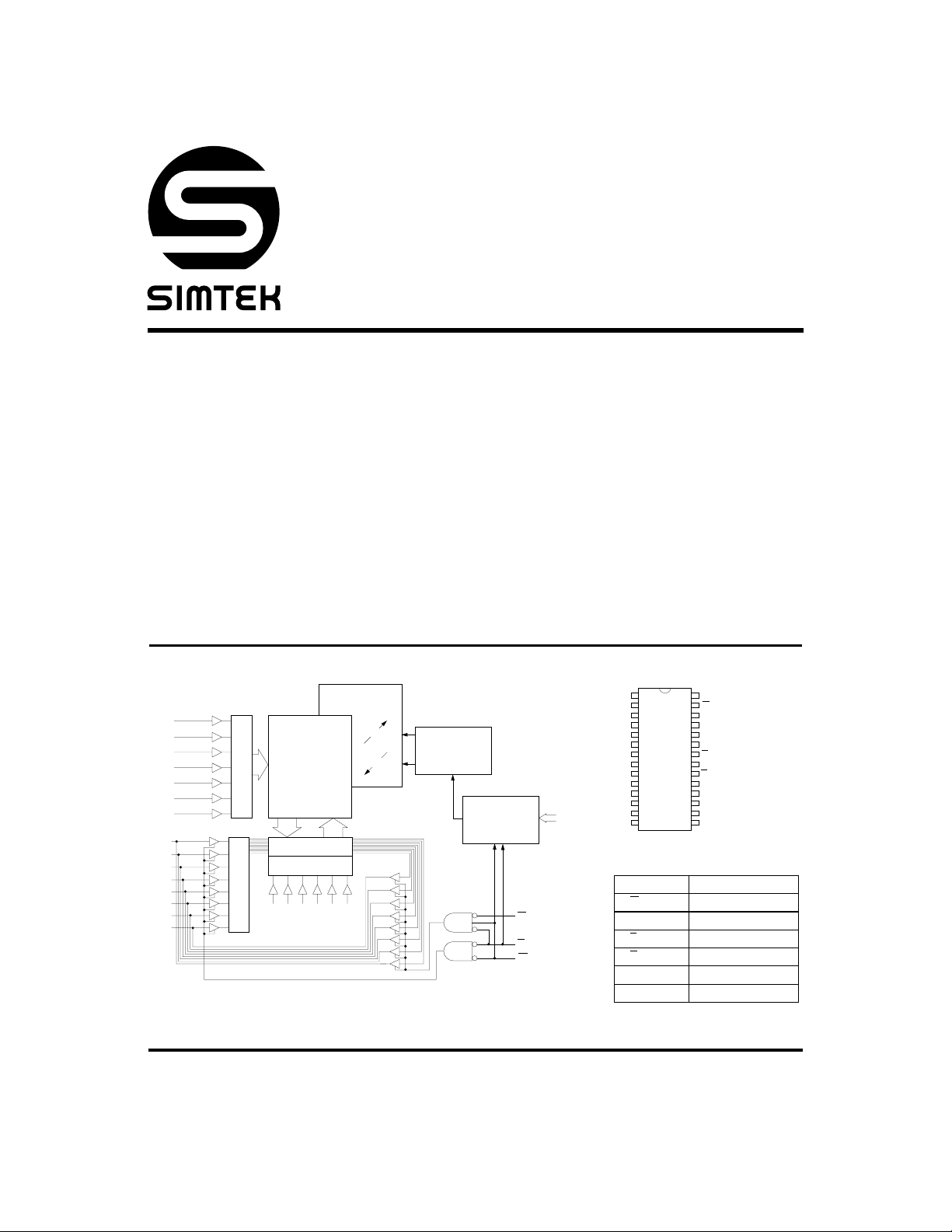
BLOCK DIAGRAM
EEPROM ARRAY
ARRAY
2
A3A
128 x 512
A
A
4
STORE
RECALL
10
STORE/
RECALL
CONTROL
DQ
DQ
DQ
DQ
DQ
DQ
DQ
DQ
A
5
A
6
A
7
A
8
A
9
A
11
A
12
0
1
2
3
4
5
6
7
STATIC RAM
ROW DECODER
COLUMN I/O
COLUMN DEC
A0A
INPUT BUFFERS
128 x 512
1
DESCRIPTION
The Simtek STK11C68 is a fast static RAM with a
nonvolatile, electrically erasable
PROM element
incorporated in each static memory cell. The
can be read and written an unlimited number of
times, while independent nonvolatile data resides in
the
EEPROM. Data transfers from the SRAM to the
EEPROM (the STORE operation), or from EEPROM to
SRAM (the RECALL operation), take place using a
software sequence. Transfers from the
the
SRAM (the RECALL operation) also take place
EEPROM to
automatically on restoration of power.
The STK11C68 is pin-compatible with industry-
standard
SRAMs. MIL-STD-883 device is also
available (STK11C68-M).
PIN CONFIGURATIONS
1
SOFTWARE
DETECT
A0-A
NC
A
12
A
7
A
6
A
5
A
4
A
3
A
2
A
1
A
0
DQ
0
DQ
1
DQ
2
12
V
SS
28
V
2
3
4
5
6
7
8
9
10
11
12
13
14
CC
27
W
26
NC
25
A
8
A
24
9
A
23
11
22
G
21
A
10
20
E
19
DQ
7
18
DQ
6
DQ
5
DQ
4
DQ
3
28 - 300 PDIP
28 - 300 CDIP
28 - 350 SOIC
17
16
15
PIN NAMES
A0 - A
12
W Write Enable
G
E
W
DQ0 - DQ
E Chip Enable
G Output Enable
V
CC
V
SS
7
Address Inputs
Data In/Out
Power (+ 5V)
Ground
SRAM
June 1999 4-21
STK11C68
ABSOLUTE MAXIMUM RATINGS
Voltage on Input Relative to VSS. . . . . . . . . . –0.6Vto (VCC+ 0.5V)
Voltage on DQ
Temperature under Bias . . . . . . . . . . . . . . . . . . . . . –55°C to 125°C
Storage Temperature . . . . . . . . . . . . . . . . . . . . . . .–65°C to 150°C
Power Dissipation. . . . . . . . . . . . . . . . . . . . . . . . . . . . . . . . . . . .1W
DC Output Current (1 output at a time, 1s duration). . . . . . . .15mA
. . . . . . . . . . . . . . . . . . . . . . –0.5V to (VCC + 0.5V)
0-7
a
Note a: Stresses greater than those listed under “Absolute Maximum
Ratings” may cause permanent damage to the device. This is a
stress ratingonly,and functional operation of thedevice atconditions above those indicated in the operational sections of this
specification is not implied. Exposure to absolute maximum rating conditions for extended periods may affect reliability.
DC CHARACTERISTICS (VCC = 5.0V ± 10%)
SYMBOL PARAMETER
c
I
I
I
I
I
I
I
V
V
V
V
T
Note b: The STK11C68-20 requires VCC = 5.0V ± 5% supply to operate at specified speed.
Note c: I
Note d: I
Note e:
Average VCC Current 100
CC
1
d
Average VCC Current during STORE 3 3 mA All Inputs Don’t Care, VCC= max
CC
2
c
Average VCC Current at t
CC
3
5V, 25˚C, Typical
e
AverageVCC Current
SB
1
(Standby, Cycling TTL Input Levels)
e
VCC Standby Current
SB
2
(Standby, Stable CMOS Input Levels)
Input Leakage Current
ILK
Off-State Output Leakage Current
OLK
Input Logic “1” Voltage 2.2 VCC + .5 2.2 VCC + .5 V All Inputs
IH
Input Logic “0” Voltage VSS – .5 0.8 VSS – .5 0.8 V All Inputs
IL
Output Logic “1” Voltage 2.4 2.4 V I
OH
Output Logic “0” Voltage 0.4 0.4 V I
OL
Operating Temperature 0 70 –40 85 °C
A
and I
CC
CC
E ≥ VIH will not produce standby current levels until any nonvolatile cycle in progress has timed out.
are dependent on output loading and cycle rate. The specified values are obtained with outputs unloaded.
CC
1
3
is the average current required for the duration of theSTORE cycle (t
2
AVAV
= 200ns
COMMERCIAL INDUSTRIAL
MIN MAX MIN MAX
N/A
STORE
N/A
).
90
75
65
28
24
21
90
75
65
10 10 mA
32
27
23
20
750 750 µA
±1 ±1 µA
±5 ±5 µA
UNITS NOTES
t
mA
mA
mA
mA
mA
mA
mA
mA
= 20ns
AVAV
t
= 25ns
AVAV
t
= 35ns
AVAV
t
= 45ns
AVAV
W ≥ (VCC– 0.2V)
All Others Cycling, CMOS Levels
t
= 20ns, E≥ V
AVAV
t
= 25ns, E ≥ V
AVAV
t
= 35ns, E≥ V
AVAV
t
= 45ns, E≥ V
AVAV
E ≥ (VCC - 0.2V)
All Others V
VCC= max
V
= VSS to V
IN
VCC= max
V
= VSS to VCC, E orG ≥ V
IN
=– 4mA
OUT
= 8mA
OUT
IH
IH
IH
IH
≤ 0.2V or ≥ (VCC – 0.2V)
IN
CC
IH
b
AC TEST CONDITIONS
Input Pulse Levels . . . . . . . . . . . . . . . . . . . . . . . . . . . . . . . 0V to 3V
Input Rise and Fall Times . . . . . . . . . . . . . . . . . . . . . . . . . . . . . . . ≤ 5ns
Input and Output Timing Reference Levels . . . . . . . . . . . . . . . 1.5V
Output Load. . . . . . . . . . . . . . . . . . . . . . . . . . . . . . . . .See Figure 1
CAPACITANCE
SYMBOL PARAMETER MAX UNITS CONDITIONS
C
IN
C
OUT
Input capacitance 8 pF ∆V = 0 to 3V
Output Capacitance 7 pF ∆V = 0 to 3V
f
(TA = 25°C, f = 1.0MHz)
Note f: These parameters are guaranteed but not tested.
June 1999 4-22
OUTPUT
5.0V
480 Ohms
30 pF
255 Ohms
INCLUDING
SCOPE AND
FIXTURE
Figure 1: AC Output Loading
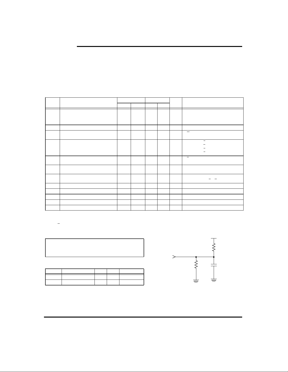
STK11C68
SRAM READ CYCLES #1 & #2 (V
NO.
SYMBOLS
#1, #2 Alt. MIN MAX MIN MAX MIN MAX MIN MAX
1t
ELQV
2t
AVAV
3t
AVQV
4t
GLQV
5t
AXQX
6t
ELQX
7t
EHQZ
8t
GLQX
9t
GHQZ
10 t
ELICCH
11 t
EHICCL
Note g: W must be high during SRAM READ cycles and low during SRAM WRITE cycles.
Note h: I/O state assumes
Note i: Measured ± 200mV from steady state output voltage.
t
ACS
g
t
RC
h
t
AA
t
OE
h
t
OH
t
LZ
i
t
HZ
t
OLZ
i
t
OHZ
f
t
PA
e, f
t
PS
E, G < VILand W > VIH; device is continuously selected.
PARAMETER
Chip Enable Access Time 20 25 35 45 ns
Read Cycle Time 20 25 35 45 ns
Address Access Time 22 25 35 45 ns
Output Enable to Data Valid 8 10 15 20 ns
Output Hold after Address Change 5555ns
Chip Enable to Output Active 5555ns
Chip Disable to Output Inactive 7 10 13 15 ns
Output Enable to Output Active 0000ns
Output Disable to Output Inactive 7 10 13 15 ns
Chip Enable to Power Active 0000ns
Chip Disable to Power Standby 25 25 35 45 ns
SRAM READ CYCLE #1: Address Controlled
ADDRESS
t
DQ (DATA OUT)
t
AXQX
5
STK11C68-20 STK11C68-25 STK11C68-35 STK11C68-45
g, h
2
t
AVAV
3
AVQV
DATA VALID
= 5.0V + 10%)
CC
b
UNITS
SRAM READ CYCLE #2: E Controlled
ADDRESS
E
t
ELQX
6
g
t
AVAV
2
t
ELQV
1
G
4
t
GLQV
8
t
GLQX
DQ (DATA OUT)
10
t
ELICCH
I
CC
STANDBY
ACTIVE
June 1999 4-23
DATA VALID
t
GHQZ
11
t
EHICCL
7
t
EHQZ
9

STK11C68
SRAM WRITE CYCLES #1 & #2 (VCC = 5.0V + 10%)
NO.
12 t
13 t
14 t
15 t
16 t
17 t
18 t
19 t
20 t
21 t
Note j: If W is low when E goes low, the outputs remain in the high-impedance state.
Note k:
SYMBOLS
#1 #2 Alt. MIN MAX MIN MAX MIN MAX MIN MAX
AVAV
WLWHtWLEH
ELWHtELEH
DVWHtDVEH
WHDXtEHDX
AVWHtAVEH
AVWL
WHAXtEHAX
WLQZ
WHQX
t
AVAV
t
AVEL
i, j
t
WC
t
WP
t
CW
t
DW
t
DH
t
AW
tASAddress Set-up to Start of Write 0 0 0 0 ns
t
WR
t
WZ
t
OW
PARAMETER
Write Cycle Time 20 25 35 45 ns
Write Pulse Width 15 20 25 30 ns
Chip Enable to End of Write 15 20 25 30 ns
Data Set-up to End of Write 8 10 12 15 ns
Data Hold after End of Write 0 0 0 0 ns
Address Set-up to End of Write 15 20 25 30 ns
Address Hold after End of Write 0 0 0 0 ns
Write Enable to Output Disable 7 10 13 15 ns
Output Active after End of Write 5 5 5 5 ns
E or W must be≥ VIH during address transitions.
SRAM WRITE CYCLE #1: W Controlled
ADDRESS
E
17
t
t
WLQZ
AVWH
13
t
WLWH
20
DATA IN
DATA OUT
18
t
AVWL
W
PREVIOUS DATA
STK11C68-20 STK11C68-25 STK11C68-35 STK11C68-45
k
12
t
AVAV
t
ELWH
14
15
t
DVWH
DATA VALID
HIGH IMPEDANCE
t
t
WHDX
19
WHAX
16
t
WHQX
UNITS
21
b
SRAM WRITE CYCLE #2: E Controlled
ADDRESS
18
t
E
W
AVEL
t
AVEH
17
k
12
t
AVAV
14
t
ELEH
t
WLEH
DATA IN
DATA OUT
HIGH IMPEDANCE
June 1999 4-24
19
t
EHAX
13
t
DVEH
15
DATA VALID
t
EHDX
16

STK11C68
STORE INHIBIT/POWER-UP RECALL (VCC = 5.0V + 10%)
NO.
22 t
23 t
24 V
25 V
Note l: t
SYMBOLS
Standard MIN MAX
RESTORE
STORE
SWITCH
RESET
starts from the time VCC rises above V
RESTORE
Power-upRECALL Duration 550 µsl
STORE Cycle Duration 10 ms
Low Voltage Trigger Level 4.0 4.5 V
Low Voltage Reset Level 3.9 V
SWITCH
PARAMETER
.
STK11C68
UNITS NOTES
STORE INHIBIT/POWER-UP RECALL
V
CC
5V
24
V
SWITCH
25
V
RESET
STORE INHIBIT
OWER-UP RECALL
DQ (DATA OUT)
22
t
RESTORE
b
POWER-UP
RECALL
BROWN OUT
STORE INHIBIT
STORE INHIBIT
NO RECALL
(V
DID NOT GO
CC
BELOW V
RESET
)
(V
BELOW V
June 1999 4-25
BROWN OUT
NO RECALL
DID NOT GO
CC
RESET
BROWN OUT
STORE INHIBIT
RECALL WHEN
V
RETURNS
CC
)
ABOVE V
SWITCH

STK11C68
SOFTWARE STORE/RECALL MODE SELECTION
E WA
LH
LH
Note m: The six consecutive addresses must be in the order listed. W must be high during all six consecutive cycles to enable a nonvolatile cycle.
SOFTWARE STORE/RECALL CYCLE
NO. SYMBOLS PARAMETER
26 t
AVAV
27 t
AVEL
28 t
ELEH
29 t
ELAX
30 t
RECALL
Note n: The software sequence is clocked with E controlled reads.
Note o: The six consecutive addresses mustbe in theorder listed inthe Software STORE/RECALL Mode Selection Table: (0000, 1555, 0AAA, 1FFF,
10F0, 0F0F) for a STORE cycle or (0000, 1555, 0AAA, 1FFF, 10F0, 0F0E) for aRECALL cycle.
cycles.
STORE/RECALL Initiation Cycle Time 20 25 35 45 ns
n
Address Set-up Time 0000ns
n
Clock Pulse Width 15 20 25 30 ns
n
Address Hold Time 15 20 20 20 ns
n
RECALL Duration 20 20 20 20 µs
SOFTWARE STORE/RECALL CYCLE: E Controlled
ADDRESS
- A0 (hex) MODE I/O NOTES
12
0000
1555
0AAA
1FFF
10F0
0F0F
0000
1555
0AAA
1FFF
10F0
0F0E
Read SRAM
Read SRAM
Read SRAM
Read SRAM
Read SRAM
Nonvolatile
STORE
Read SRAM
Read SRAM
Read SRAM
Read SRAM
Read SRAM
Nonvolatile
RECALL
n, o
STK11C68-20 STK11C68-25 STK11C68-35 STK11C68-45
MIN MAX MIN MAX MIN MAX MIN MAX
Output Data
Output Data
Output Data
Output Data
Output Data
Output High Z
Output Data
Output Data
Output Data
Output Data
Output Data
Output High Z
(VCC = 5.0V ± 10%)
W must be high during all six consecutive
o
t
AVAV
26
26
t
AVAV
ADDRESS #6ADDRESS #1
m
m
UNITS
b
DQ (DATA OUT)
27
t
E
AVEL
28
t
ELEH
29
t
ELAX
DATA VALID
June 1999 4-26
DATA VALID
23 30
t
/ t
STORE
HIGH IMPEDANCE
RECALL

DEVICE OPERATION
STK11C68
The STK11C68 is a versatile memory chip that provides several modes of operation. The STK11C68
can operate as a standard 8K x 8
8K x 8
EEPROM shadow to which the SRAM informa-
tion can be copied or from which the
SRAM. It has an
SRAM can be
updated in nonvolatile mode.
NOISE CONSIDERATIONS
Note that the STK11C68 is a high-speed memory
and so must have a high-frequency bypass capacitor of approximately 0.1µF connected between V
and Vss, using leads and traces that are as short as
possible. As with all high-speed
CMOS ICs, normal
careful routing of power,groundandsignalswillhelp
prevent noise problems.
SRAM READ
The STK11C68 performs a READ cycle whenever E
and
G are low and W is high. The address specified
on pins A
bytes will be accessed. When the
determines which of the 8,192 data
0-12
READ is initiated
by an address transition, the outputs will be valid
after a delay of
initiated by
at
t
, whichever is later (READ cycle #2). The data
GLQV
t
(READ cycle #1). If the READ is
AVQV
EorG, the outputs will be validat t
ELQV
outputs will repeatedly respond to address changes
within the t
access time without the need for tran-
AVQV
sitions on any control input pins, and will remain valid
until another address change or until
EorGis
brought high.
SRAM WRITE
A WRITE cycle is performed whenever E and W are
low. The address inputs must be stable prior to
entering the
until either
The data on the common I/O pins DQ
ten into the memory if it is valid t
of a
W controlled WRITE or t
E controlled WRITE.
It is recommended that
entire
the common I/O lines. If
will turn off the output buffers t
WRITE cycle and must remain stable
EorW goes high at the end of the cycle.
will be writ-
0-7
before the end
DVWH
before the end of an
DVEH
G be kept high during the
WRITE cycle to avoid data bus contention on
G is left low,internal circuitry
after W goes low.
WLQZ
SOFTWARE NONVOLATILE STORE
The STK11C68 software STORE cycle is initiated by
executing sequential
address locations. During the
READ cycles from six specific
STORE cycle an erase
of the previous nonvolatile data is first performed,
followed by a program of the nonvolatile elements.
The program operation copies the
nonvolatilememory. Once a
SRAM data into
STORE cycle is initiated,
further input and output are disabled until the cycle
is completed.
cc
Because a sequence of
addresses is used for
tant that no other
READ or WRITE accesses inter-
READs from specific
STORE initiation, it is impor-
vene in the sequence or the sequence will be
aborted and no
To initiate the software
READ sequence must be performed:
1. Read address 0000 (hex) Valid READ
2. Read address 1555 (hex) Valid READ
3. Read address 0AAA (hex) Valid READ
4. Read address 1FFF (hex) Valid READ
5. Read address 10F0 (hex) Valid READ
6. Read address 0F0F (hex) Initiate STORE cycle
STORE or RECALL will take place.
STORE cycle, the following
or
The software sequence must be clockedwith E controlled
READs.
Once the sixth address in the sequence has been
entered, the STORE cycle will commence and the
chip will be disabled. It is important that
and not
although it is not necessary that
sequence to be valid. After the t
been fulfilled, the
READ and WRITE operation.
WRITE cycles be used in the sequence,
G be low for the
STORE
SRAM will again be activated for
SOFTWARE NONVOLATILE RECALL
A software RECALL cycle is initiated with a sequence
of
READ operations in a manner similar to the soft-
ware
STORE initiation. To initiate the RECALL cycle,
the following sequence of
performed:
1. Read address 0000 (hex) Valid READ
2. Read address 1555 (hex) Valid READ
3. Read address 0AAA (hex) Valid READ
4. Read address 1FFF (hex) Valid READ
5. Read address 10F0 (hex) Valid READ
6. Read address 0F0E (hex) Initiate RECALL cycle
READ operations must be
READ cycles
cycle time has
June 1999 4-27
STK11C68
Internally, RECALL is a two-step procedure. First,
the
SRAM data is cleared, and second, the nonvola-
tile information is transferred into the
After the t
be ready for
RECALL operation in no way alters the data in the
EEPROM cells. The nonvolatile data can be recalled
cycle time the SRAM will once again
RECALL
READ and WRITE operations. The
SRAM cells.
an unlimited number of times.
POWER-UP RECALL
During power up, or after any low-power condition
(V
CC<VRESET
latched. When V
voltage of V
be initiated and will take t
If the STK11C68 is in a
power-up
To help avoid this situation, a 10K Ohm resistor
should be connected either between
V
or between E and system VCC.
CC
), an internal RECALL request will be
once again exceeds the sense
CC
,aRECALL cycle will automatically
SWITCH
RECALL, the SRAM data will be corrupted.
to complete.
RESTORE
WRITE state at the end of
W and system
100
80
HARDWARE PROTECT
The STK11C68 offers hardware protection against
inadvertent
conditions. When V
STORE operation during low-voltage
CC
<V
, software STORE
SWITCH
operations are inhibited.
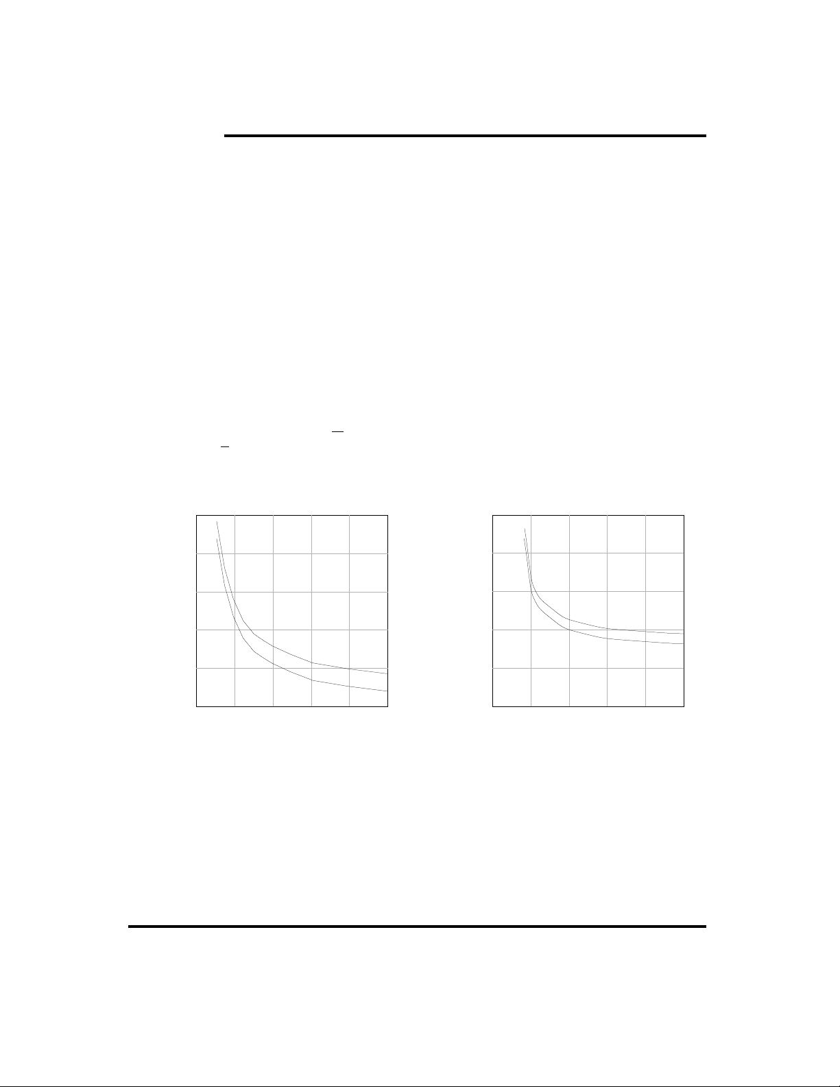
LOW AVERAGE ACTIVE POWER
The STK11C68 draws significantly less current
when it is cycled at times longer than 50ns. Figure 2
shows the relationship between I
time. Worst-case current consumption is shown for
both
CMOS and TTL input levels (commercial tem-
perature range, V
= 5.5V, 100% duty cycle on chip
CC
enable). Figure 3 shows the same relationship for
WRITE cycles. If the chip enable duty cycle is less
than 100%, only standby current is drawn when the
chip is disabled. The overall average current drawn
by the STK11C68 depends on the following items:
1)
CMOS vs. TTL input levels; 2) the duty cycle of
chip enable; 3) the overall cycle rate for accesses;
4) the ratio of
temperature; 6) the V
100
80
READstoWRITEs; 5) the operating
level; and 7) I/O loading.
cc
and READ cycle
CC
60
40
20
Average Active Current (mA)
0
Figure 2: I
50 100 150 200
Cycle Time (ns)
(max) Reads
CC
TTL
CMOS
June 1999 4-28
60
40
20
Average Active Current (mA)
0
50 100 150 200
Figure 3: ICC (max) Writes
TTL
CMOS
Cycle Time (ns)

ORDERING INFORMATION
STK11C68
STK11C68
- P 25 I
Temperature Range
Blank = Commercial (0 to 70˚C)
I = Industrial (–40 to 85˚C
Access Time
20 = 20ns (Commercial only)
25 = 25ns
35 = 35ns
45 = 45ns
Package
P = Plastic 28-pin 300 mil DIP
C = Ceramic 28-pin 300 mil DIP
S = Plastic 28-pin 350 mil SOIC
)
June 1999 4-29

STK11C68
June 1999 4-30
 Loading...