

SIMTEK STK11C68-5C45M, STK11C68-5C35M, STK11C68-5L55M, STK11C68-5L45M, STK11C68-5K55M Datasheet
...
STK11C68-M
4-31
STK11C68-M
CMOS nvSRAM
High Performance
8K x 8 Nonvolatile Static RAM
MIL-STD-883/SMD # 5962-92324
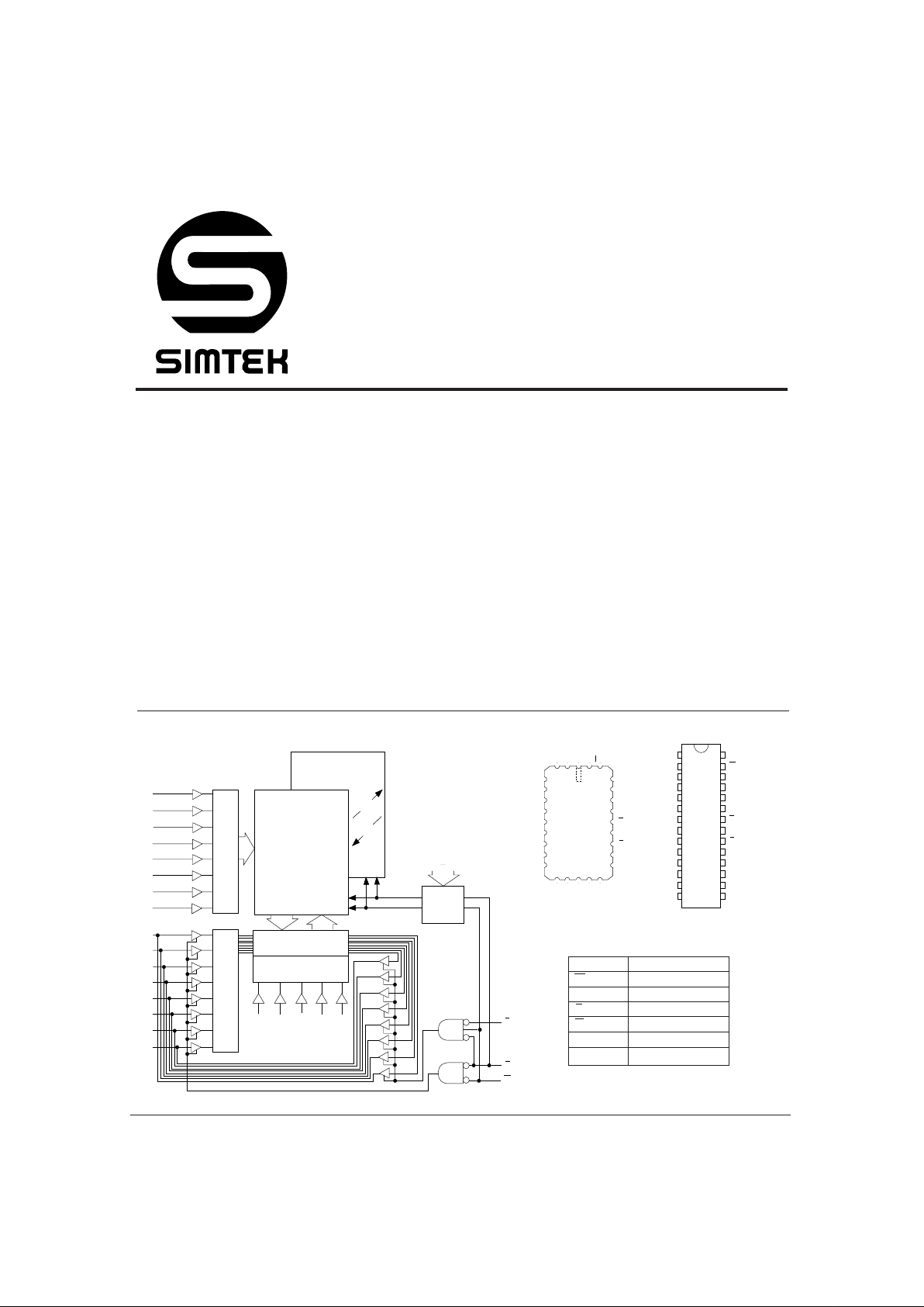
LOGIC BLOCK DIAGRAM PIN CONFIGURATIONS
1
2
3
4
5
6
7
8
9
10
11
12
13
14
28
27
26
25
24
23
22
21
20
19
18
17
16
15
NC
A
A
A
A
A
A
A
A
DQ
DQ
DQ
DQ
DQ
DQ
DQ
DQ
V
V
W
NC
A
A
G
A
E
SS
7
6
5
4
3
2
1
0
0
1
2
8
9
10
7
6
5
4
3
CC
A
11
A
12
28 - 300 C-DIP
28 - LCC
PIN NAMES
A
A
A
A
A
A
4
5
6
7
8
EEPROM ARRAY
256 x 256
STORE
RECALL
STATIC RAM
ARRAY
256 x 256
ROW DECODER
STORE/
RECALL
CONTROL
AAAAA
0
1210
12
DQ
DQ
DQ
DQ
DQ
DQ
DQ
DQ
0
1
2
3
4
5
6
7
G
E
W
COLUMN I/O
COLUMN DECODER
INPUT BUFFERS
AA
011
A
3
A
9
12
A0 - A
12
Address Inputs
W Write Enable
DQ0 - DQ7Data In/Out
E Chip Enable
G Output Enable
V
CC
Power (+5V)
V
SS
Ground
DESCRIPTION
The Simtek STK11C68-M is a fast static RAM (35, 45
and 55ns), with a nonvolatile electrically-erasable PROM
(EEPROM) element incorporated in each static memory
cell. The SRAM can be read and written an unlimited
number of times, while independent nonvolatile data
resides in EEPROM. Data transfers from the SRAM to
the EEPROM (
STORE
), or from the EEPROM to the
SRAM (
RECALL
) are initiated through software sequences. It combines the high performance and ease
of use of a fast SRAM with nonvolatile data integrity.
The STK11C68-M is pin compatible with industry standard SRAMs and is available in a 28-pin 300 mil
ceramic DIP or 28-pad LCC package. Commercial and
industrial devices are also available.
FEATURES
• 35, 45 and 55ns Access Times
• 17, 20 and 25ns Output Enable Access
• Unlimited Read and Write to SRAM
• Software
STORE
Initiation
• Automatic
STORE
Timing
• 100,000
STORE
cycles to EEPROM
• 10 year data retention in EEPROM
• Automatic
RECALL
on Power Up
• Software
RECALL
Initiation
• Unlimited
RECALL
cycles from EEPROM
• Single 5V ± 10% Operation
• Available in multiple standard packages
A
A
A
A
A
A
A
A
A
A
A
A
DQ
DQ
DQDQDQ
DQ
DQ
G
A
E
DQ
Vss
NC
Vcc
W
NC
7
12
6
5
4
3
2
1
0
0
1
8
9
11
10
7
6
234
5
TOP VIEW
4
5
6
7
8
9
10
11
12
32128 27
26
25
24
23
22
21
20
19
18
1716151413
STK11C68-M
4-32
I
CC
b
Average VCC Current 90 mA t
AVAV
= 35ns
85 mA t
AVAV
= 45ns
80 mA t
AVAV
= 55ns
I
CC
d
Average VCC Current 50 mA E ≥ (VCC – 0.2V)
during STORE cycle all others VIN ≤ 0.2V or ≥ (VCC – 0.2V)
I
SB
c
Average VCC Current 27 mA t
AVAV
= 35ns
(Standby, Cycling TTL Input Levels) 23 mA t
AVAV
= 45ns
20 mA t
AVAV
= 55ns
E ≥ VIH; all others cycling
I
SB
c
Average VCC Current 2 mA E ≥ (VCC – 0.2V)
(Standby, Stable CMOS Input Levels) all others VIN ≤ 0.2V or ≥ (VCC – 0.2V)
I
ILK
Input Leakage Current (Any Input) ±1 µAVCC = max
VIN = VSS to V
CC
I
OLK
Off State Output Leakage Current ±5 µAVCC = max
VIN = VSS to V
CC
V
IH
Input Logic "1" Voltage 2.2 VCC+.5 V All Inputs
V
IL
Input Logic "0" Voltage VSS–.5 0.8 V All Inputs
V
OH
Output Logic "1" Voltage 2.4 V I
OUT
= –4mA
V
OL
Output Logic "0" Voltage 0.4 V I
OUT
= 8mA
T
A
Operating Temperature –55 125 °C
ABSOLUTE MAXIMUM RATINGS
a
Voltage on typical input relative to VSS. . . . . . . . . . . . . –0.6V to 7.0V
Voltage on DQ
0-7
and G. . . . . . . . . . . . . . . . . . .–0.5V to (VCC+0.5V)
Temperature under bias . . . . . . . . . . . . . . . . . . . . . . –55°C to 125°C
Storage temperature. . . . . . . . . . . . . . . . . . . . . . . . . –65°C to 150°C
Power dissipation. . . . . . . . . . . . . . . . . . . . . . . . . . . . . . . . . . . . . .1W
DC output current . . . . . . . . . . . . . . . . . . . . . . . . . . . . . . . . . . .15mA
Note a: Stresses greater than those listed under "Absolute Maximum
Ratings" may cause permanent damage to the device. This is a stress
rating only, and functional operation of the device at conditions above
those indicated in the operational sections of this specification is not
implied. Exposure to absolute maximum rating conditions for extended
periods may affect reliability.
(One output at a time, one second duration)
DC CHARACTERISTICS (VCC = 5.0V ± 10%)
AC TEST CONDITIONS
Input Pulse Levels. . . . . . . . . . . . . . . . . . . . . . . . . . . . . VSS to 3V
Input Rise and Fall Times. . . . . . . . . . . . . . . . . . . . . . . . . . ≤ 5ns
Input and Output Timing Reference Levels. . . . . . . . . . . . . . 1.5V
Output Load. . . . . . . . . . . . . . . . . . . . . . . . . . . . . . . See Figure 1
CAPACITANCEe (T
A
=25°C, f=1.0MHz)
Note e: These parameters are guaranteed but not tested. Figure 1: AC Output Loading
5.0V
Output
480 Ohms
30pF
INCLUDING
SCOPE
AND FIXTURE
255 Ohms
C
IN
Input Capacitance 5 pF ∆V = 0 to 3V
C
OUT
Output Capacitance 7 pF ∆V = 0 to 3V
SYMBOL PARAMETER MAX UNITS CONDITIONS
1
2
1
2
SYMBOL PARAMETER MIN MAX UNITS NOTES
Note b: ICC is dependent on output loading and cycle rate. The specified values are obtained with outputs unloaded.
Note c: Bringing E ≥ VIH will not produce standby current levels until any nonvolatile cycle in progress has timed out. See MODE SELECTION table.
Note d: I
CC
is the average current required for the duration of the store cycle (t
STORE
) after the sequence (tWC) that initiates the cycle.
2
1
STK11C68-M
4-33
#1, #2 Alt. MIN MAX MIN MAX MIN MAX
NO. PARAMETER UNITS
(VCC = 5.0V ± 10%)
Note c: Bringing E high will not produce standby currents until any nonvolatile cycle in progress has timed out. See MODE SELECTION table.
Note e: Parameter guaranteed but not tested.
Note g: For READ CYCLE #1 and #2, W must be high for entire cycle.
Note h: Device is continuously selected with E low and G low.
Note i: Measured ± 200mV from steady state output voltage.
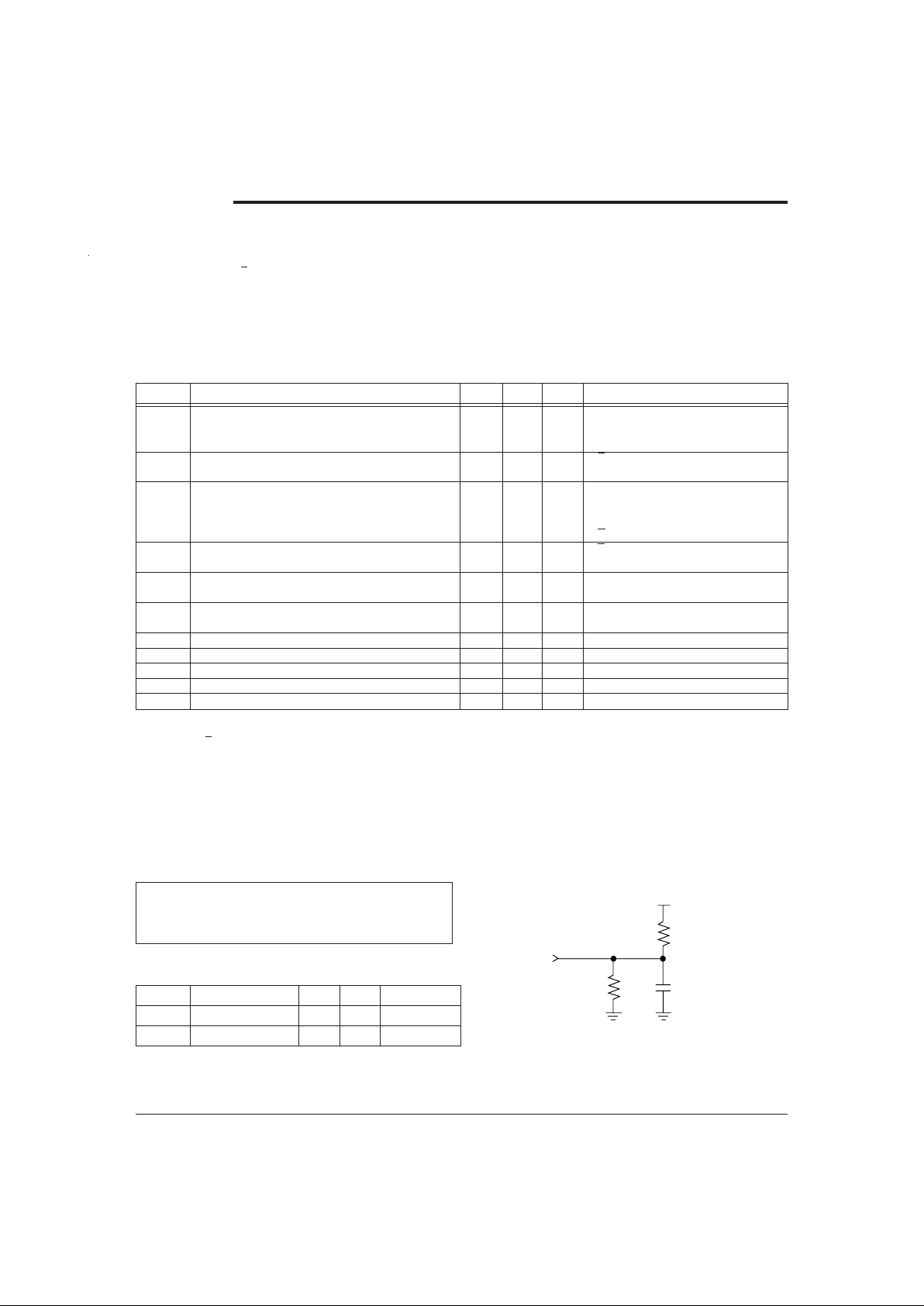
READ CYCLE #1
g,h
W
DQ (Data Out)
ADDRESS
DATA VALID
5
t
AXQX
11A
t
WHQV
2
t
AVAV
3
t
AVQV
READ CYCLE #2
g
ADDRESS
E
G
DQ (Data Out)
DATA VALID
I
CC
W
2
t
AVAV
1
t
ELQV
6
t
ELQX
4
t
GLQV
8
t
GLQX
11
t
EHICCL
7
t
EHQZ
9
t
GHQZ
10
t
ELICCH
11A
t
WHQV
ACTIVE
STANDBY
READ CYCLES #1 & #2
1t
ELQV
t
ACS
Chip Enable Access Time 35 45 55 ns
2t
AVAV
g
t
RC
Read Cycle Time 35 45 55 ns
3t
AVQV
h
t
AA
Address Access Time 35 45 55 ns
4t
GLQV
t
OE
Output Enable to Data Valid 20 25 25 ns
5t
AXQX
t
OH
Output Hold After Address Change 5 5 5 ns
6t
ELQX
t
LZ
Chip Enable to Output Active 5 5 5 ns
7t
EHQZ
i
t
HZ
Chip Disable to Output Inactive 17 20 25 ns
8t
GLQX
t
OLZ
Output Enable to Output Active 0 0 0 ns
9t
GHQZ
i
t
OHZ
Output Disable to Output Inactive 17 20 25 ns
10 t
ELICCH
e
t
PA
Chip Enable to Power Active 0 0 0 ns
11 t
EHICCL
c,e
t
PS
Chip Disable to Power Standby 35 45 55 ns
11A t
WHQV
t
WR
Write Recovery Time 45 55 65 ns
SYMBOLS STK11C68-35M STK11C68-45M STK11C68-55M

STK11C68-M
4-34
#1 #2 Alt. MIN MAX MIN MAX MIN MAX
SYMBOLS STK11C68-35M STK11C68-45M STK11C68-55M
NO. PARAMETER UNITS
#1 #2 Alt. MIN MAX MIN MAX MIN MAX
NO. PARAMETER UNITS
WRITE CYCLES #1 & #2; G low
SYMBOLS STK11C68-35M STK11C68-45M STK11C68-55M
12 t
AVAVtAVAVtWC
Write Cycle Time 35 45 55 ns
13 t
WLWHtWLEHtWP
Write Pulse Width 30 35 45 ns
14 t
ELWHtELEHtCW
Chip Enable to End of Write 30 35 45 ns
15 t
DVWHtDVEHtDW
Data Set-up to End of Write 18 20 30 ns
16 t
WHDXtEHDXtDH
Data Hold After End of Write 0 0 0 ns
17 t
AVWHtAVEHtAW
Address Set-up to End of Write 30 35 45 ns
18 t
AVWLtAVELtAS
Address Set-up to Start of Write 0 0 0 ns
19 t
WHAXtEHAXtWR
Address Hold After End of Write 0 0 0 ns
WRITE CYCLES #1 & #2; G high
(VCC = 5.0V ± 10%)
12 t
AVAVtAVAVtWC
Write Cycle Time 45 45 55 ns
13 t
WLWHtWLEHtWP
Write Pulse Width 35 35 45 ns
14 t
ELWHtELEHtCW
Chip Enable to End of Write 35 35 45 ns
15 t
DVWHtDVEHtDW
Data Set-up to End of Write 30 30 30 ns
16 t
WHDXtEHDXtDH
Data Hold After End of Write 0 0 0 ns
17 t
AVWHtAVEHtAW
Address Set-up to End of Write 35 35 45 ns
18 t
AVWLtAVELtAS
Address Set-up to Start of Write 0 0 0 ns
19 t
WHAXtEHAXtWR
Address Hold After End of Write 0 0 0 ns
20 t
WLQZ
i,m
tWZWrite Enable to Output Disable 35 35 35 ns
21 t
WHQX
tOWOutput Active After End of Write 5 5 5 ns
Note i: Measured + 200mV from steady state output voltage.
Note k: E or W must be ≥ V
IH
during address transitions.
Note m: If W is low when E goes low, the outputs remain in the high impedance state.
(VCC = 5.0V ± 10%)

STK11C68-M
4-35
PREVIOUS DATA
ADDRESS
E
W
DATA IN
DATA OUT
DATA VALID
HIGH IMPEDANCE
12
t
AVAV
14
t
ELWH
19
t
WHAX
17
t
AVWH
18
t
AVWL
13
t
WLWH
15
t
DVWH
16
t
WHDX
20
t
WLQZ
21
t
WHQX
WRITE CYCLE #1: W CONTROLLED
k
ADDRESS
E
W
DATA IN
DATA OUT
HIGH IMPEDANCE
DATA VALID
12
t
AVAV
18
t
AVEL
14
t
ELEH
19
t
EHAX
17
t
AVEH
13
t
WLEH
15
t
DVEH
16
t
EHDX
WRITE CYCLE #2: E CONTROLLED
k
STK11C68-M
4-36
Note n: The six consecutive addresses must be in order listed - (0000, 1555, 0AAA, 1FFF, 10F0, 0F0F) for a
STORE
cycle or (0000, 1555, 0AAA,1FFF, 10F0, 0F0E)
for a
RECALL
cycle. W must be high during all six consecutive cycles. See
STORE
cycle and
RECALL
cycle tables and diagrams for further details.
Note o: I/O state assumes that G ≤ VIL. Initiation and operation of nonvolatile cycles does not depend on the state of G.
STORE
CYCLE INHIBIT and AUTOMATIC POWER-UP
RECALL
MODE SELECTION
NONVOLATILE MEMORY OPERATION
H X X Not Selected Output High Z Standby
L H X Read SRAM Output Data Active o
L L X Write SRAM Input Data Active
L H 0000 Read SRAM Output Data Active n,o
1555 Read SRAM Output Data n,o
0AAA Read SRAM Output Data n,o
1FFF Read SRAM Output Data n,o
10F0 Read SRAM Output Data n,o
0F0F Nonvolatile
STORE
Output High Z I
CC
n
L H 0000 Read SRAM Output Data Active n,o
1555 Read SRAM Output Data n,o
0AAA Read SRAM Output Data n,o
1FFF Read SRAM Output Data n,o
10F0 Read SRAM Output Data n,o
0F0E Nonvolatile
RECALL
Output High Z n
EW A
12
- A0(hex) MODE I/O POWER NOTES
2
4.0
5.0V
t
STORE
inhibit
Automatic
RECALL
V
CC

STK11C68-M
4-37
#1 Alt. MIN MAX MIN MAX MIN MAX
(VCC = 5.0V ± 10%)
STORE/RECALL CYCLE
22 t
AVAVtRC
STORE/RECALL
Initiation Cycle Time 35 45 55 ns
23 t
ELQZ
p
Chip Enable to Output Inactive 75 75 85 ns
24 t
ELQXS
t
STORE
q
STORE
Cycle Time 10 10 10 ms
25 t
ELQXR
t
RECALL
r
RECALL
Cycle Time 20 20 20 µs
26 t
AVELN
s
t
AE
Address Set-up to Chip Enable 0 0 0 ns
27 t
ELEHN
s,t
t
EP
Chip Enable Pulse Width 25 35 45 ns
28 t
EHAXN
s
t
EA
Chip Disable to Address Change 0 0 0 ns
SYMBOLS STK11C68-35M STK11C68-45M STK11C68-55M
NO. PARAMETER UNITS
Note p: Once the software
STORE
or
RECALL
cycle is initiated, it completes automatically, ignoring all inputs.
Note q: Note that
STORE
cycles (but not
RECALLs
) are aborted by VCC < 4.0V (STORE inhibit).
Note r: A
RECALL
cycle is initiated automatically at power up when VCC exceeds 4.0V. t
RECALL
is measured from the point at which VCC exceeds 4.5V.
Note s: Noise on the E pin may trigger multiple read cycles from the same address and abort the address sequence.
Note t: If the Chip Enable Pulse Width is less than t
ELQV
(see READ CYCLE #2) but greater than or equal to t
ELEHN
, then the data may not be valid at the end of
the low pulse, however the
STORE
or
RECALL
will still be initiated.
Note u: W must be HIGH when E is LOW during the address sequence in order to initiate a nonvolatile cycle. G may be either HIGH or LOW throughout.
Addresses #1 through #6 are found in the MODE SELECTION table. Address #6 determines whether the STK11C68-M performs a
STORE
or
RECALL
.
Note v: E must be used to clock in the address sequence for the Software
STORE
and
RECALL
cycles.
STORE/RECALL CYCLE
u,v
ADDRESS
E
DATA OUT
DATA VALID
ADDRESS #6
ADDRESS #1
DATA VALID
HIGH IMPEDANCE
22
t
AVAV
22
t
AVAV
26
t
AVELN
27
t
ELEHN
28
t
EHAXN
24
t
STORE
25
t
RECALL
23
t
ELQZ

STK11C68-M
4-38
The STK11C68-M has two separate modes of operation: SRAM mode and nonvolatile mode. In SRAM
mode, the memory operates as an ordinary static
RAM. In nonvolatile operation, data is transferred from
SRAM to EEPROM or from EEPROM to SRAM. In this
mode SRAM functions are disabled.
SRAM READ
The STK11C68-M performs a READ cycle whenever
E and G are LOW while W is HIGH. The address
specified on pins A
0-12
determines which of the 8192
data bytes will be accessed. When the READ is
initiated by an address transition, the outputs will be
valid after a delay of t
AVQV
(READ CYCLE #1). If the
READ is initiated by E or G, the outputs will be valid at
t
ELQV
or at t
GLQV
, whichever is later (READ CYCLE #2).
The data outputs will repeatedly respond to address
changes within the t
AVQV
access time without the need
for transitions on any control input pins, and will remain
valid until another address change or until E or G is
brought HIGH or W is brought LOW.
The STK11C68-M is a high speed memory and therefore must have a high frequency bypass capacitor of
approximately 0.1µF connected between DUT V
CC
and VSS using leads and traces that are as short as
possible. As with all high speed CMOS ICs, normal
careful routing of power, ground and signals will help
prevent noise problems.
SRAM WRITE
A write cycle is performed whenever E and W are
LOW. The address inputs must be stable prior to
entering the WRITE cycle and must remain stable until
either E or W go HIGH at the end of the cycle. The
data on pins DQ
0-7
will be written into the memory if it
is valid t
DVWH
before the end of a W controlled WRITE
or t
DVEH
before the end of an E controlled WRITE.
It is recommended that G be kept HIGH during the
entire WRITE cycle to avoid data bus contention on
common I/O lines. If G is left LOW, internal circuitry will
turn off the output buffers t
WLQZ
after W goes LOW.
NONVOLATILE STORE
The STK11C68-M
STORE
cycle is initiated by executing sequential READ cycles from six specific address
locations. By relying on READ cycles only, the
STK11C68-M implements nonvolatile operation while
remaining pin-for-pin compatible with standard 8Kx8
SRAMs. During the
STORE
cycle, an erase of the
previous nonvolatile data is first performed, followed
by a program of the nonvolatile elements. The program operation copies the SRAM data into nonvolatile
elements. Once a
STORE
cycle is initiated, further
input and output are disabled until the cycle is completed.
Because a sequence of reads from specific addresses
is used for
STORE
initiation, it is important that no
other read or write accesses intervene in the sequence
or the sequence will be aborted and no
STORE
or
RECALL
will take place.
To initiate the
STORE
cycle the following READ se-
quence must be performed:
1. Read address 0000 (hex) Valid READ
2. Read address 1555 (hex) Valid READ
3. Read address 0AAA (hex) Valid READ
4. Read address 1FFF (hex) Valid READ
5. Read address 10F0 (hex) Valid READ
6. Read address 0F0F (hex) Initiate
STORE
Cycle
Once the sixth address in the sequence has been
entered, the
STORE
cycle will commence and the chip
will be disabled. It is important that READ cycles and
not WRITE cycles be used in the sequence, although
it is not necessary that G be LOW for the sequence to
be valid. After the t
STORE
cycle time has been fulfilled,
the SRAM will again be activated for READ and WRITE
operation.
HARDWARE PROTECT
The STK11C68-M offers hardware protection against
inadvertent
STORE
cycles through V
CC
Sense. A
STORE
cycle will not be initiated, and one in progress
will discontinue, if VCC goes below 4.0V. 4.0V is a
typical, characterized value. The datasheet specifica-
tions are guaranteed only for VCC = 5.0 +10%.
NONVOLATILE RECALL
A
RECALL
cycle of the EEPROM data into the SRAM
is initiated with a sequence of READ operations in a
manner similar to the
STORE
initiation. To initiate the
RECALL
cycle the following sequence of READ op-
erations must be performed:
1. Read address 0000 (hex) Valid READ
2. Read address 1555 (hex) Valid READ
3. Read address 0AAA (hex) Valid READ
4. Read address 1FFF (hex) Valid READ
5. Read address 10F0 (hex) Valid READ
6. Read address 0F0E (hex) Initiate
RECALL
Cycle
DEVICE OPERATION

STK11C68-M
4-39
Internally,
RECALL
is a two step procedure. First, the
SRAM data is cleared and second, the nonvolatile
information is transferred into the SRAM cells. The
RECALL
operation in no way alters the data in the
EEPROM cells. The nonvolatile data can be recalled
an unlimited number of times.
On power-up, once VCC exceeds the VCC sense voltage of 4.0V, a
RECALL
cycle is automatically initiated.
The voltage on the VCC pin must not drop below 4.0V
once it has risen above it in order for the
RECALL
to
operate properly. Due to this automatic
RECALL
,
SRAM operation cannot commence until t
RECALL
after
VCC exceeds 4.0V. 4.0V is a typical, characterized
value.
If the STK11C68-M is in a WRITE state at the end of
power-up
RECALL
, the SRAM data will be corrupted.
To help avoid this situation, a 10K Ohm resistor should
be connected between W and system VCC.

STK11C68-M
4-40
Temperature Range
M = Military (-55 to 125 degrees C)
Access Time
35 = 35ns
45 = 45ns
55 = 55ns
Package
C = Ceramic 28 pin 300-mil DIP with gold lead finish
K = Ceramic 28 pin 300-mil DIP with solder DIP finish
L = Ceramic 28 pin LCC
Retention / Endurance
10 years / 100,000 cycles
STK11C68 - 5 C 35 M
Lead Finish
A =Solder DIP lead finish
C =Gold lead DIP finish
X =lead finish "A" or "C" is acceptable
Package
MX = Ceramic 28 pin 300-mil DIP
MY = Ceramic 28 pin LCC
Access Time
04 = 55ns
05 = 45ns
06 = 35ns
5962-92324 04 MX X
ORDERING INFORMATION
 Loading...