

SIMTEK STK10C48-S45, STK10C48-S45I, STK10C48-S35I, STK10C48-S35, STK10C48-S25 Datasheet
...
STK10C48
2K x 8 nvSRAM
QuantumTrap™ CMOS
Nonvolatile Static RAM
FEATURES
• 20ns, 25ns, 35ns and 45ns Access Times
• STORE to EEPROM Initiated by Hardware
• RECALL to SRAM Initiated by Hardware or
Power Restore
• Automatic STORE Timing
• 10mA T ypical I
at 200ns Cycle Time
CC
• Unlimited READ, WRITE and RECALL Cycles
• 1,000,000 STORE Cycles to EEPROM
• 100-Year Data Retention over Full Industrial
Temperature Range
• Commercial and Industrial Temperatures
• 28-Pin 300 mil PDIP, 300 mil SOIC and
350 mil SOIC Packages
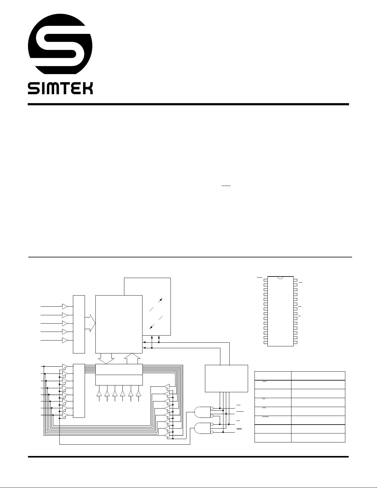
BLOCK DIAGRAM
EEPROM ARRAY
32 x 512
A
5
A
6
A
7
A
8
A
9
ROW DECODER
STATIC R AM
ARRAY
32 x 512
STORE
RECALL
DESCRIPTION
The Simtek STK10C48 is a fast static RAM with a non-
volatile electrically erasable
incorporated in each static memory cell. The
PROM (EEPROM) element
SRAM
can be read and written an unlimited number of times,
while independent nonvolatile data resides in
EEPROM. Data may easily be transferred from the
SRAM to the EEPROM (the STORE operation), or from
the
EEPROM to the SRAM (the RECALL operation),
using the NE
pin. Transfers from the EEPROM to the
SRAM (the RECALL operation) also take place auto-
matically on restoration of power. The STK10C48
combines the high performance and ease of use of a
fast
SRAM with nonvolatile data integrity.
The STK10C48 features industry-standard pinout for
nonvolatile
RAMs.
PIN CONFIGURATIONS
1
DQ
DQ
DQ
V
NC
NE
2
3
A
7
A
4
6
A
5
5
A
6
4
A
7
3
8
A
2
9
A
1
10
A
0
11
0
12
1
13
2
14
SS
V
28
CC
W
27
26
NC
25
A
8
A
24
9
NC
23
22
G
21
A
10
20
E
19
DQ
7
18
DQ
6
17
DQ
5
DQ
DQ
4
3
28 - 300 PDIP
28 - 300 SOIC
28 - 350 SOIC
16
15
DQ
DQ
DQ
DQ
DQ
DQ
DQ
DQ
0
1
2
3
4
5
6
7
INPUT BUFFERS
COLUMN I/O
COLUMN DEC
A
A
A0A
2
1
A
A
3
4
10
July 1999 3-1
STORE/
RECALL
CONTROL
PIN NAMES
G
NE
E
W
A0 - A
10
W Write Enable
DQ0 - DQ
E Chip Enable
G Output Enable
NE Nonvolatile Enable
V
CC
V
SS
7
Address Inputs
Data In/Out
Power (+ 5V)
Ground
STK10C48
ABSOLUTE MAXIMUM RATINGS
Volt age on Input Rel ative to VSS. . . . . . . . . . –0.6V to (VCC + 0.5V)
Volt age on DQ
Temperature under Bias . . . . . . . . . . . . . . . . . . . . . –55°C to 125°C
Storage Temperature . . . . . . . . . . . . . . . . . . . . . . . –65°C to 150°C
Power Dissipation . . . . . . . . . . . . . . . . . . . . . . . . . . . . . . . . . . . . 1W
DC Output Current (1 output at a time, 1s duration). . . . . . . . 15m A
. . . . . . . . . . . . . . . . . . . . . . –0.5V to (VCC + 0.5V)
0-7
a
Note a: Stresses greater than those listed under “Absolute Maximum
Ratings” may cause permanent damage to the device. This is a
stress rating only, and functional operation of the device at conditions above those indicated in the operational sections of this
specification is not implied. Exposure to absolute maximum rating conditions for extended periods may affect reliability.
DC CHARACTERISTICS (VCC = 5.0V ± 10%)
SYMBOL PARAMETER
c
I
CC
I
CC
I
CC
I
SB
I
SB
I
ILK
I
OLK
V
V
V
V
T
IH
IL
OH
OL
A
Average VCC Current 95
1
d
Average VCC Current during STORE 33mAAll Inputs Don’t Care, VCC = max
2
c
Average VCC Current at t
3
5V, 25°C, Typical
e
Average VCC Current
1
(Standby, Cycling TTL Input Levels)
e
VCC Standby Current
2
(Standby, Stable CMOS Input Levels )
Input Leakage Current
Off-State Output Leakage Current
Input Logic “1” Volta ge 2.2 V
Input Logic “0” Volta ge VSS – .5 0.8 VSS – .5 0. 8 V All Inputs
Output Logic “1” Voltage 2.4 2.4 V I
Output Logic “0” Voltage 0.4 0.4 V I
Operating Temperature 0 70 –40 85 °C
AVAV
= 200ns
Note b: The STK10C48-20 requires VCC = 5.0V ± 5% supply to operate at specified speed.
Note c: I
Note d: I
Note e: E
and I
CC
1
is the average current required for the duration of the STORE cycle (t
CC
2
≥ VIH will not produce standby current levels until any nonvolatile cycle in progress has timed out.
are dependent on output loading and cycle rate. The specified values are obtained with outputs unloaded.
CC
3
COMMERCIAL INDUSTRIAL
MIN MAX MIN MAX
N/A
STORE
90
75
65
N/A
26
22
19
).
85
75
65
10 10 mA
30
25
21
18
750 750 µA
±1 ±1 µA
±5 ±5 µA
+ .5 2.2 VCC + .5 V All Inputs
CC
UNITS NOTES
mA
mA
mA
mA
mA
mA
mA
mA
t
= 20ns
AVAV
t
= 25ns
AVAV
t
= 35ns
AVAV
t
= 45ns
AVAV
W
≥ (V
– 0.2V)
CC
All Others Cycling, CMOS Levels
t
= 20ns, E ≥ V
AVAV
t
= 25ns, E ≥ V
AVAV
t
= 35ns, E ≥ V
AVAV
t
= 45ns, E ≥ V
AVAV
E
≥ (VCC – 0.2V)
All Others V
V
= max
CC
V
= VSS to V
IN
V
= max
CC
V
= V
IN
SS
= –4mA
OUT
= 8mA
OUT
IH
IH
IH
IH
≤ 0.2V or ≥ (VCC – 0.2V)
IN
CC
to VCC, E or G ≥ VIH
b
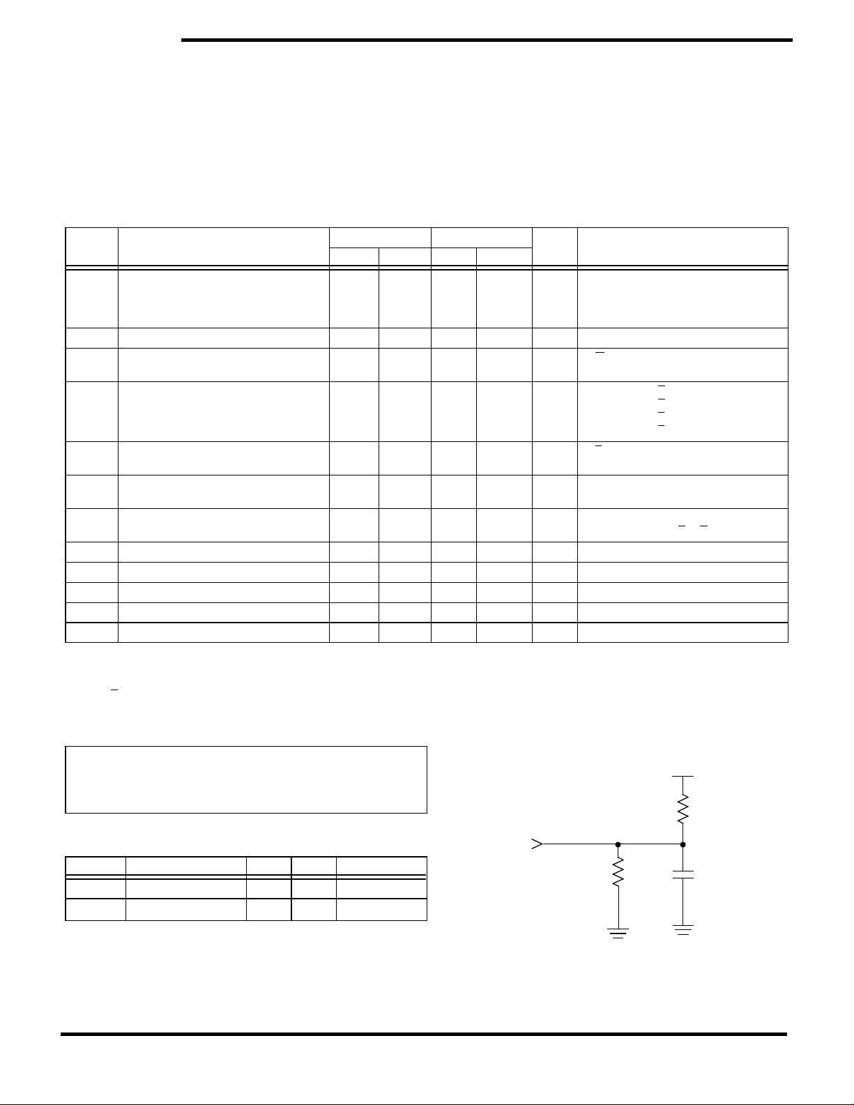
AC TEST CONDITIONS
Input Pulse Levels . . . . . . . . . . . . . . . . . . . . . . . . . . . . . . . 0V to 3V
Input Rise and Fall Times . . . . . . . . . . . . . . . . . . . . . . . . . . . . . . . ≤ 5ns
Input and Output Timing Reference Levels. . . . . . . . . . . . . . . 1.5V
Output Load. . . . . . . . . . . . . . . . . . . . . . . . . . . . . . . . .See Figure 1
CAPACITANCE
SYMBOL PARAMETER MAX UNITS CONDITIONS
C
C
IN
OUT
Input Capacitance
Output Capacitance
f
(TA = 25°C, f = 1.0MHz)
8pF
7pF
∆V = 0 to 3V
∆V = 0 to 3V
Note f: These parameters are guaranteed but not tested.
July 1999 3-2
OUTPUT
5.0V
480 Ohms
30 pF
255 Ohms
INCLUDING
SCOPE AND
FIXTURE
Figure 1: AC Output Loading
STK10C48
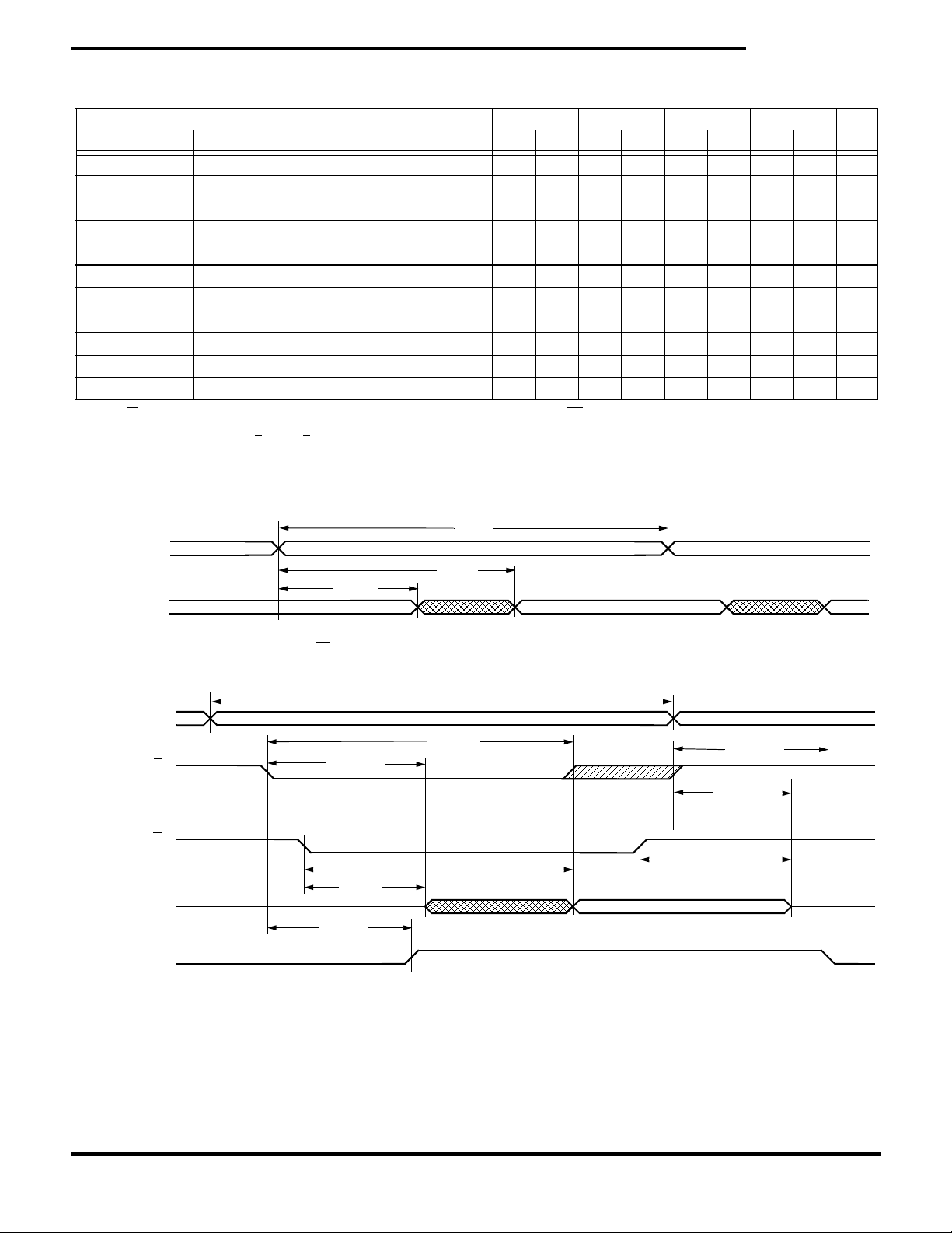
SRAM READ CYCLES #1 & #2 (V
NO.
10 t
11 t
#1, #2 Alt. MIN MAX MIN MAX MIN MAX MIN MAX
1t
ELQV
2t
AVAV
3t
AVQV
4t
GLQV
5t
AXQX
6t
ELQX
7t
EHQZ
8t
GLQX
9t
GHQZ
ELICCH
EHICCL
SYMBOLS
g
h
h
i
i
f
e, f
t
ACS
t
RC
t
AA
t
OE
t
OH
t
LZ
t
HZ
t
OLZ
t
OHZ
t
PA
t
PS
PARAMETER
Chip Enable Access Time 20 25 35 45 ns
Read Cycle Time 20 25 35 45 ns
Address Access Time 22 25 35 45 ns
Output Enable to Data Valid 8 10 15 20 ns
Output Hol d after Address Change 5 5 5 5 ns
Chip Enable to Output Active 5 5 5 5 ns
Chip Disable to Output Inactive 7 10 13 15 ns
Output Enable to Output Active 0 0 0 0 ns
Output Disa ble to Outpu t Inactive 7 10 13 15 ns
Chip Enable to Power Active 0 0 0 0 ns
Chip Disable to Power Standby 25 25 35 45 ns
STK10C48-20 STK10C48-25 STK10C48-35 STK10C48-45
= 5.0V ± 10%)
CC
Note g: W must be high during SRAM READ cycles and low during SRAM WRITE cycles. NE must be high during entire cycle.
Note h: I/O state assumes E
Note i: Measured +
SRAM READ CYCLE #1: Address Controlled
, G < VIL, W > VIH , and NE ≥ VIH; device is continuously selected.
200mV from steady state output voltage.
2
t
AVAV
g, h
ADDRESS
3
t
AVQV
DATA VALID
DQ (DATA OUT)
t
AXQX
5
b
UNITS
SRAM READ CYCLE #2: E Controlled
ADDRESS
t
ELQX
t
ELICCH
6
t
GLQX
10
4
t
GLQV
8
DQ (DATA OUT)
I
CC
E
G
STANDBY
g
t
AVAV
2
t
ELQV
ACTIVE
1
t
GHQZ
DATA VALID
t
9
7
EHQZ
t
EHICCL
11
July 1999 3-3

STK10C48
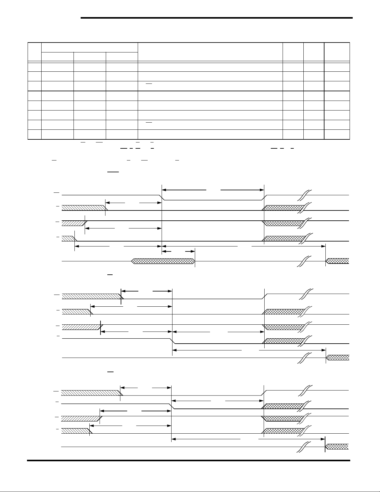
SRAM WRITE CYCLES #1 & #2 (V
NO.
12 t
13 t
14 t
15 t
16 t
17 t
18 t
19 t
20 t
21 t
WLWH
ELWH
DVWH
WHDX
AVWH
AVWL
WHAX
WLQZ
WHQX
SYMBOLS
#1 #2 Alt. MIN MAX MIN MAX MIN MAX MIN MAX
AVAV
t
AVAV
t
WLEH
t
ELEH
t
DVEH
t
EHDX
t
AVEH
t
AVEL
t
EHAX
i, j
t
Write Cycle Time 20 25 35 45 ns
WC
t
Write Pulse Width 15 20 25 30 ns
WP
t
Chip Enable to End of Write 15 20 25 30 ns
CW
t
Data Set-up to End of Write 8 10 12 15 ns
DW
t
Data Hold after End of Write 0 0 0 0 ns
DH
t
Address Set-up to End of Wri te 15 20 25 30 ns
AW
t
Address Set-up to Start of Write 0 0 0 0 ns
AS
t
Address Hold after En d of Write 0 0 0 0 ns
WR
t
Write Enable to Output Disable 7 10 13 15 ns
WZ
t
Output Active afte r En d of Write 5 5 5 5 ns
OW
PARAMETER
Note j: If W is low when E goes low, the outputs remain in the high-impedance state.
Note k: E
or W must be ≥ VIH during address transitions. NE ≥ VIH.
SRAM WRITE CYCLE #1: W Controlled
ADDRESS
t
E
ELWH
STK10C48-20 STK10C48-25 STK10C48-35 STK10C48-45
k
12
t
AVAV
14
19
t
WHAX
= 5.0V ± 10%)
CC
b
UNITS
17
t
20
t
WLQZ
AVWH
13
t
WLWH
W
DATA IN
DA TA OUT
t
AVWL
18
PREVIOUS DATA
SRAM WRITE CYCLE #2: E Controlled
ADDRESS
18
t
AVEL
E
17
t
AVEH
W
DATA IN
15
t
DVWH
DATA VALID
HIGH IMPEDANCE
16
t
WHDX
21
t
WHQX
k
12
t
AVAV
t
ELEH
14
13
t
WLEH
15
t
DVEH
DATA VALID
t
EHAX
t
EHDX
19
16
DA TA OUT
HIGH IMPEDANCE
July 1999 3-4

MODE SELECTION
E W G NE MODE POWER
H X X X Not Selected Standby
L H L H Read SRAM Active
L L X H Write SRAM Active
L H L L Nonvolatile RECALL
L L H L Nonvolatile STORE I
L
L
L
H
L
H
L
X
No Operation Active
l
STK10C48
Active
CC
2
Note l: An automatic RECALL takes place at power up, starting when VCC exceeds 4.25V and taking t
RESTORE
.
STORE CYCLES #1 & #2 (VCC = 5.0V ± 10%)
NO.
22 t
23 t
24
25 t
26 t
27 t
28 t
#1 #2 Alt.
WLQX
WLNH
t
GHNL
NLWL
ELWL
Note m: Measured with W and NE both returned high, and G returned low. STORE cycles are inhibited below 4.0V.
Note n: Once t
the STORE initiation cycle.
Note o: If E
is low for any period of time in which W is high while G and NE are low, then a RECALL cycle may be initiated.
STORE CYCLE #1: W Controlled
NE
G
W
SYMBOLS
m
n
WC
t
ELQX
t
ELNH
GHEL
t
NLEL
WLEL
t
STORE
t
WC
STORE Cycle Time 10 ms
STORE Initiation Cycle Time 20 ns
Output Disable Set-up to NE Fall 5 ns
Output Disable Set-up to E Fal l 5 ns
NE Set-up 5 ns
Chip Enable Set-up 5 ns
Write Enable Set-up 5 ns
has been satisfied by NE, G, W and E, the STORE cycle is completed automatically. Any of NE, G, W or E may be used to terminate
PARAMETER MIN MAX UNITS
o
24
t
GHNL
26
t
NLWL
23
t
WLNH
b
27
t
E
DQ (DATA OUT)
STORE CYCLE #2: E Controlled
NE
G
W
E
DQ (DATA OUT)
HIGH IMPEDANCE
ELWL
HIGH IMPEDANCE
26
t
NLEL
25
t
GHEL
28
t
WLEL
o
July 1999 3-5
23
t
ELNH
t
WLQX
22
t
ELQX
22
STK10C48
RECALL CYCLES #1, #2 & #3 (V
NO.
29 t
30 t
#1 #2 #3
NLQX
NLNH
31 t
t
32
GLNL
33 t
WHNL
34 t
ELNL
35 t
NLQZ
36 t
RESTORE
Note p: Measured with W and NE both high, and G and E low.
Note q: Once t
the RECALL initiation cycle.
Note r: If W
is low at any point in which both E and NE are low and G is high, then a STORE cycle will be initiated instead of a RECALL.
RECALL CYCLE #1: NE Controlled
NE
G
SYMBOLS
p
q
t
ELQX
t
ELNH
NLEL
t
GLEL
t
WHEL
t
GLEL
t
GLQX
t
GLNH
t
NLGL
t
WHGL
t
ELGL
RECALL Cycle Time 20 µs
RECALL Initiation Cycle Time 20 ns
NE Set-up 5 ns
Output Enable Set-up 5 ns
Write Enable Set-up 5 ns
Chip Enable Set-up 5 ns
PARAMETER MIN MAX UNITS
NE Fall to Outputs Inactive 20 ns
Power-up RECALL Duration 550 µs
has been satisfied by NE, G, W and E, the RECALL cycle is completed automatically. Any of NE, G or E may be used to terminate
NLNH
o
30
t
NLNH
32
t
GLNL
= 5.0V ± 10%)
CC
b
W
E
DQ (DATA OUT)
RECALL CYCLE #2: E Controlled
NE
G
W
E
DQ (DATA OUT)
33
t
WHNL
34
t
ELNL
32
t
GLEL
33
t
WHEL
HIGH IMPEDANCE
t
NLEL
o
31
RECALL CYCLE #3: G Controlledo,
31
t
34
t
ELGL
33
t
WHGL
NLGL
NE
DQ (DATA OUT)
G
W
E
HIGH IMPEDANCE
29
35
t
NLQZ
t
ELNH
30
t
NLQX
HIGH IMPEDANCE
29
t
ELQX
r
30
t
GLNH
29
t
GLQX
July 1999 3-6

DEVICE OPERATION
STK10C48
The STK10C48 has two modes of operation: SRAM
mode and nonvolatile mode, determined by the
state of the NE
ory operates as a standard fast static
pin. When in SRAM mode, the mem-
RAM. While in
nonvolatile mode, data is transferred in parallel from
SRAM to EEPROM or from EEPROM to SRAM.
NOISE CONSIDERATIONS
Note that the STK10C48 is a high-speed memory
and so must have a high-frequency bypass capacitor of approximately 0.1µF connected between V
CC
and VSS, using leads and traces that are as short as
possible. As with all high-speed
CMOS ICs, normal
careful routing of power, ground and signals will
help prevent noise problems.
SRAM READ
The STK10C48 performs a READ cycle whenever E
and G are low and NE and W are high. The address
specified on pins A
data bytes will be accessed. When the
determines which of the 2,048
0-10
READ is initi-
ated by an address transition, the outputs will be
valid after a delay of t
READ is initiated by E or G, the outputs will be valid
at t
ELQV
or at t
, whichever is later (READ cycle #2 ) .
GLQV
(READ cycle #1). If the
AVQV
The data outputs will repeatedly respond to address
changes within the t
access time without the need
AVQV
for transitions on any control input pins, and will
remain valid until another address change or until E
or G is brought high or W or NE is brought low.
SRAM WRITE
A WRITE cycle is performed whenever E and W are
low and NE
ble prior to entering the
remain stable until either E
end of the cycle. The data on pins DQ
ten into the memory if it is valid t
of a W
E
controlled WRITE.
It is recommended that G
entire
the common I/ O li nes. If G
will turn off the output buffers t
is high. The address inputs must be sta-
WRITE cycle and must
or W goes high at the
will be writ-
0-7
before the end
DVWH
controlled WRITE or t
before the end of an
DVEH
be kept high during the
WRITE cycle to avoid data bus contention on
is left low, internal circuitry
after W goes low.
WLQZ
NONVOLATILE STORE
A STORE cycle is performed when NE, E and W and
low and G
achieves this state will initiate a
ation (
is high. While any sequence that
STORE, only W initi-
STORE cycle #1) and E initi ation (STORE cycle
#2) are practical without risking an unintentional
SRAM WRITE that would disturb SRAM data. During a
STORE cycle, previous nonvolatile data is erased
and the
nonvolatile elements. Once a
SRAM contents are then programmed into
STORE cycle is initi-
ated, further input and output are disabled and the
DQ
pins are tri-stated until the cycle is complete.
0-7
and G are low and W and NE are high at the end
If E
of the cycle, a
puts will go active, signaling the end of the
READ will be performed and the out-
STORE.
NONVOLATILE RECALL
A RECALL cycle is performed when E, G and NE are
low and W
is high. Like the STORE cycle, RECALL is
initiated when the last of the four clock signals goes
to the
cycle will take t
inputs are ignored. When the
any
RECALL state. Once initiated, the RECALL
to complete, during which all
NLQX
RECALL completes,
READ or WRITE state on the input pins will take
effect.
Internally, RECALL is a two-step procedure. First, the
SRAM data is cleared, and second, the nonvolatile
information is transferred into the
RECALL operation in no way alters the data in the
SRAM cells. The
nonvolatile cells. The nonvolatile data can be
recalled an unlimited number of times.
As with the
any one control pin to cause a
inadvertent multi-triggering. On power up, once V
STORE cycle, a transition must occur on
RECALL, preventing
CC
exceeds 4.25V, a RECALL cycle is automatically initiated. Due to this automatic
tion cannot commence until t
RECALL, SRAM opera-
after V
RESTORE
CC
exceeds 4.25V.
POWER-UP RECALL
During power up, or after any low-power condition
(V
< 3.0V), an internal RECALL request will be
CC
latched. When V
RECALL cycle will automatically be initiated and will
take t
RESTORE
to complete.
once again exceeds 4.25V, a
CC
July 1999 3-7

STK10C48
If the STK10C48 is in a WRITE state at the end of
power-up
RECALL, the SRAM data will be corrupted.
To help avoid this situation, a 10K Ohm resistor
should be connected either between W
V
or between E and system VCC.
CC
and system
HARDWARE PROTECT
The STK10C48 offers two levels of protection to
suppress inadvertent
signals (E
, G, W and NE) remain in the STORE con-
dition at the end of a
STORE cycle will not be started. The STORE (or
RECALL) will be initiated only after a transition on
any one of these signals to the required state. In
addition to multi-trigger protection,
inhibited when V
against inadvertent
100
STORE cycles. If the control
STORE cycle, a second
STOREs are
is below 4.0V, protecting
CC
STOREs.
LOW AVERAGE ACTIVE POWER
The STK10C48 draws significantly less current
when it is cycled at times longer than 55ns. Figure 2
shows the relationship between I
time. Worst-case current consumption is shown for
both
CMOS and TTL input levels (commercial tem-
perature range, V
= 5.5V, 100% duty cycle on
CC
chip enable). Figure 3 shows the same relationship
for
WRITE cycles. If the chip enable duty cycle is
less than 100%, only standby current is drawn
when the chip is disabled. The overall average current drawn by the STK10C48 depends on the following items: 1)
CMOS vs. TTL input levels; 2) the
duty cycle of chip enable; 3) the overall cycle rate
for accesses; 4) the ratio of
the operating temperature; 6) the V
O loading.
100
and READ cycle
CC
READs to WRITEs; 5)
level; and 7) I/
CC
Average Active Current (mA)
80
60
40
20
0
50 100 150 200
Cycle Time (ns)
Figure 2: I
(max) Reads
CC
TTL
CMOS
Average Active Current (mA)
80
60
40
20
0
50 100 150 200
Cycle Time (ns)
Figure 3: ICC (max) Writes
TTL
CMOS
July 1999 3-8

ORDERING INFOR M ATION
STK10C48
STK10C48
- P 25 I
Temperature Range
Blank = Commercial (0 to 70°C)
I = Industrial (–40 to 85°C
Access Time
20 = 20ns (Commercial only)
25 = 25ns
35 = 35ns
45 = 45ns
Package
P = Plastic 28-pin 300 mil DIP
N = Plastic 28-pin 300 mil SOIC
S = Plastic 28-pin 350 mil SOIC
)
July 1999 3-9
 Loading...