

Page 1

Xfin Blade
SERVICE MANUAL
XFIN-BLADE-SM
Issue 1.0
October 2006
© Team Simoco 2006
Team Simoco Ltd.
Field House,
Uttoxeter Old Road
Derby
DE1 1NH
Tel: +44 (0) 1332 375 500
FAX: +44 (0) 1332 375 501
www.teamsimoco.com
Page 2
PAGE 2 DECLARATION
DECLARATION
The performance figures quoted are subject to normal manufacturing and service
tolerances. The right is reserved to alter the equipment described in this manual in the
light of future technical development.
COPYRIGHT
All rights reserved. No part of this publication may be reproduced in any form or by any
means without the prior written permission of Team Simoco Ltd.
ERRORS AND OMISSIONS
The usefulness of this publication depends upon the accuracy and completeness of the
information contained within it. Whilst every endeavour has been made to eliminate any
errors, some may still exist. It is requested that any errors or omissions noted should be
reported to:
Technical Documentation
Team Simoco Ltd
Field House
Uttoxeter Old Road
Derby
DE1 1NH
UK
Tel: +(44) 01332 375 627
E-mail: [email protected]
DOCUMENT HISTORY
Issue Date Comments
0.1 Sept 2005 Skeleton document created.
0.2 Mar 2006 Draft submitted for internal review by Development.
0.3 Apr 2006 Diagrams added.
0.4 Aug 2006 Product Variants and Spares information received.
1.0 Nov 2006
Added details on PSTN & RJ45 serial ports, E&M linking
corrected.
Page 3
XFIN-BLADE-SM
WARNINGS AND CAUTIONS PAGE 3
WARNINGS AND CAUTIONS
WARNING
The Power Amplifier Module uses semiconductor devices containing Beryllium
Oxide. Dust from this oxide is toxic and, if inhaled or skin contact is made, can
be hazardous to health.
No danger can arise from normal handling, but no attempt should be made to
break open or tamper with these devices in any way.
These items should not be discarded with industrial or domestic waste.
Caution
During disassembly and assembly, refer to the ‘Torque Settings’ section in this
manual.
Caution
Preparing the radio for alignment will erase from the radio all customer PMR and
Trunking configuration data (channel, signalling information etc). The only data
retained by the Alignment Tool is the factory alignment data for the radio (DAC
settings for TX power, front-end tuning etc).
WARNING
To avoid RF injury, do not touch the Antenna when the Transmitter is in use.
Do not operate transmitter with antenna disconnected – RF burn hazard.
WARNING
The weight of a fully assembled Base Station in the wall mount is approx 10kg.
Two people should be used to lift the unit in this form.
WARNING
When drilling walls, check first for any buried cables or pipes.
WARNING
Disconnect Mains Electricity before working on the unit with wall-mount or rack
p
ower supplies open.
Page 4

PAGE 4 TABLE OF CONTENTS
TABLE OF CONTENTS
DECLARATION...............................................................................................................2
COPYRIGHT ...................................................................................................................2
ERRORS AND OMISSIONS ...........................................................................................2
DOCUMENT HISTORY ...................................................................................................2
WARNINGS AND CAUTIONS ........................................................................................3
TABLE OF CONTENTS ..................................................................................................4
1 INTRODUCTION..................................................................................................... 8
1.1 General.................................................................................................................8
2 PRODUCT CODES.................................................................................................9
2.1 Serial number ......................................................................................................9
2.1.1 Hardware Variant Code.......................................................................................9
2.1.2 MAC Address......................................................................................................9
2.1.3 Modification State ...............................................................................................9
3 DESCRIPTION...................................................................................................... 11
3.1 Ventilation.......................................................................................................... 11
3.2 SRM9000 Sub-assembly...................................................................................12
3.3 Specifications....................................................................................................12
3.3.1 General ............................................................................................................. 12
3.3.2 Transmitter ........................................................................................................ 13
3.3.3 Receiver............................................................................................................14
3.4 Front Panel Controls.........................................................................................14
3.4.1 LED Indicators .................................................................................................. 14
3.4.2 LCD...................................................................................................................14
3.4.3 Control Knob.....................................................................................................15
3.4.4 MMI RJ45 Connector........................................................................................16
3.5 Rear Panel Connectors..................................................................................... 16
3.5.1 Tx/Rx................................................................................................................. 17
3.5.2 Power................................................................................................................17
3.5.3 Fuses ................................................................................................................18
3.5.4 Ethernet ............................................................................................................18
3.5.5 RS232 Serial (D-Sub) .......................................................................................19
3.5.6 RS232 Serial (RJ45).........................................................................................19
3.5.7 USB Connector.................................................................................................19
Page 5

XFIN-BLADE-SM
TABLE OF CONTENTS PAGE 5
3.5.8 Line 1 & 2 (RJ45)..............................................................................................19
3.5.9 Facilities............................................................................................................ 20
3.5.10 PSTN Port (RJ11) ............................................................................................. 21
4 TECHNICAL DESCRIPTION ................................................................................ 23
4.1 MMI Board.......................................................................................................... 23
4.1.1 Description ........................................................................................................24
4.2 Control Board.................................................................................................... 25
4.2.1 Circuit Board Layout ......................................................................................... 25
4.2.2 Circuit Description............................................................................................. 26
4.2.2.1 LEDs....................................................................................................... 26
4.2.2.2 Test Points..............................................................................................26
4.2.2.3 DSP ........................................................................................................30
4.2.2.4 Power......................................................................................................31
4.2.2.5 IXP.......................................................................................................... 31
4.2.2.6 CoDec.....................................................................................................32
4.2.2.7 Audio Interface........................................................................................ 32
4.2.2.8 PSTN Interface ....................................................................................... 33
4.2.3 Links ................................................................................................................. 33
4.3 Receiver and Transmitter Modules .................................................................36
4.3.1 Frequency Bands.............................................................................................. 36
4.3.2 Receiver............................................................................................................36
4.3.2.1 Front-end Filters and Rx Front-end Amplifier..........................................36
4.3.2.2 First Mixer and IF Section....................................................................... 38
4.3.2.3 Quadrature Demodulator ........................................................................ 38
4.3.2.4 Receiver Audio Processing.....................................................................38
4.3.3 Transmitter........................................................................................................ 38
4.3.3.1 Drivers and PA Stages............................................................................39
4.3.3.2 Tx Power Control ....................................................................................41
4.3.3.3 Antenna Changeover and Harmonic Filter..............................................41
4.3.3.4 Transmitter Audio Processing.................................................................41
4.3.4 Frequency Synthesis ........................................................................................ 42
4.3.4.1 General................................................................................................... 42
4.3.4.2 PLL .........................................................................................................42
4.3.4.3 VCO........................................................................................................ 42
4.3.4.4 Negative Bias Generator and Loop Filter................................................42
4.3.4.5 Phase Modulator..................................................................................... 43
4.3.4.6 Reference Oscillator ...............................................................................43
4.3.5 RF Sub-Assembly Internal Control Logic .......................................................... 45
4.3.5.1 DSP and FPGA....................................................................................... 46
4.3.5.2 DSP Clock Oscillator...............................................................................46
4.3.6 RF Sub-Assembly Internal Memory ..................................................................46
4.3.6.1 Multiplexer ..............................................................................................46
4.3.7 RF Sub-Assembly Internal Power Supplies ......................................................47
4.3.7.1 Power On Function .................................................................................47
4.3.7.2 Power Lines ............................................................................................ 47
Page 6

PAGE 6 TABLE OF CONTENTS
4.4 Antenna Requirements.....................................................................................49
4.5 Power supplies..................................................................................................49
4.6 Configuration.....................................................................................................49
4.7 Adjustment and Alignment...............................................................................49
5 MAINTENANCE....................................................................................................51
5.1 Torque Settings.................................................................................................51
5.2 Disassembly ......................................................................................................51
5.2.1 To Remove the Blade from a Rack ................................................................... 51
5.2.2 To Open the Blade............................................................................................ 52
5.2.3 To Remove a Tx or Rx Assembly .....................................................................52
5.2.4 To Remove the Control Board ..........................................................................53
5.2.5 To Remove the Front Assembly........................................................................53
5.2.6 To Remove the MMI Board ...............................................................................54
5.2.7 To Remove a Fan .............................................................................................54
5.3 Re-Assembly .....................................................................................................54
5.3.1 To Fit an MMI Board .........................................................................................54
5.3.2 To Fit the Front Assembly .................................................................................54
5.3.3 To Fit the Control Board....................................................................................54
6 PRODUCT VARIANTS AND ACCESSORIES......................................................55
6.1 Variants..............................................................................................................55
6.2 Accessories .......................................................................................................55
6.2.1 TSF-ACCORD ..................................................................................................56
6.2.2 Duplexers, Combiners, Cavities, RSA Units .....................................................56
6.2.3 TSF-EARS ........................................................................................................57
6.2.4 TSF-PROG ....................................................................................................... 57
6.2.5 Blade Shelves...................................................................................................57
6.2.6 TSF-1BS PSUTRAY .........................................................................................57
6.2.6.1 TSF-1BS PSUTRAY Specifications ........................................................ 57
7 SPARES ...............................................................................................................59
7.1 Service Concept ................................................................................................ 59
7.2 Level-2 Spares Schedule..................................................................................60
7.2.1 XFIN BLADE (INTERNAL PSU VERSION).......................................................60
7.2.2 Assembly Item List ............................................................................................61
7.3 Warranty.............................................................................................................62
7.3.1 Service Within and Out Of Warranty.................................................................62
7.3.2 Ancillary Items...................................................................................................62
7.3.3 Unpacking Equipment.......................................................................................62
7.4 Software Policy .................................................................................................63
Page 7

XFIN-BLADE-SM
TABLE OF CONTENTS PAGE 7
8 LCD MENU OPERATION..................................................................................... 65
8.1 Default Display ..................................................................................................65
8.2 Menu Structure.................................................................................................. 65
8.2.1 Alarms Menu.....................................................................................................66
8.2.2 Set IP Address ..................................................................................................66
8.2.3 Set Position in Site............................................................................................ 66
8.2.4 Set Site ID.........................................................................................................66
8.2.5 Set System ID................................................................................................... 66
8.2.6 Enable Screen Saver........................................................................................ 66
8.2.7 Test Menu......................................................................................................... 66
8.2.8 Exit ....................................................................................................................66
9 PROGRAMMER GUIDE .......................................................................................67
9.1 Getting Started ..................................................................................................67
9.1.1 Main Screen......................................................................................................67
9.2 Database ............................................................................................................ 67
9.2.1 Creating a New Database................................................................................. 67
9.2.2 Opening a Database.........................................................................................68
9.3 Communications Settings................................................................................68
9.3.1 Connection Type............................................................................................... 68
9.3.2 Serial Communications ..................................................................................... 68
9.3.3 Ethernet Communications................................................................................. 69
9.3.4 Open Comms....................................................................................................69
9.4 State ................................................................................................................... 69
9.5 Area Configuration............................................................................................70
9.5.1 Edit....................................................................................................................70
9.5.2 Add ................................................................................................................... 70
9.5.3 Delete ............................................................................................................... 70
9.5.4 Accept/Send...................................................................................................... 70
9.5.5 Get Record ....................................................................................................... 70
9.5.6 Send Configuration ...........................................................................................70
9.5.7 Get Configuration..............................................................................................71
9.5.8 Reset Configuration .......................................................................................... 71
9.5.9 Navigation Buttons............................................................................................ 71
A. GLOSSARY AND ABBREVIATIONS................................................................... 74
B. CONTROL CARD BLOCK DIAGRAM .................................................................75
Page 8
PAGE 8 INTRODUCTION
1 INTRODUCTION
1.1 GENERAL
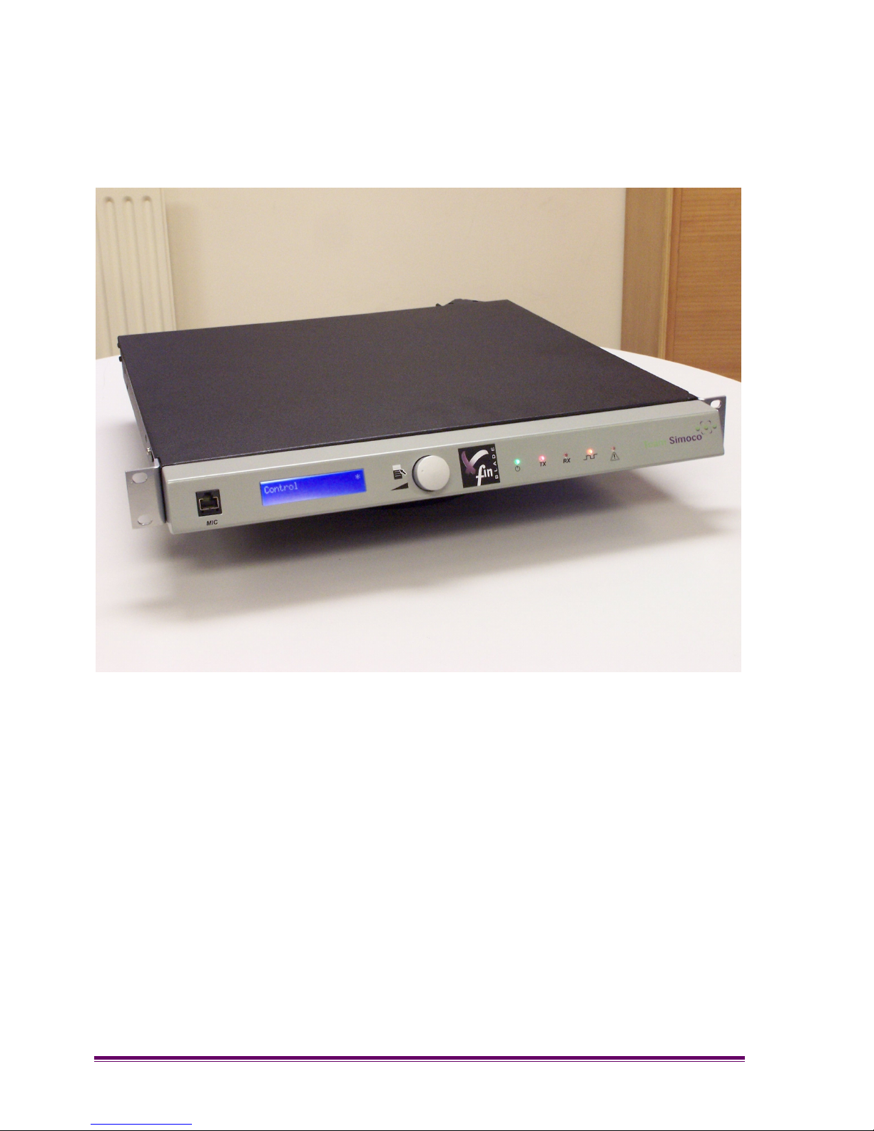
Figure 1.1 - Front view of the Xfin Blade.
Brief Description: The Xfin Blade is a 1U trunking system with an integrated basestation
and the capability to provide a control and/or traffic channel. It incorporates the
established MPT1327 trunking standard with next generation hardware and VoIP
technology. A trunked site consists of a number of Blade units which are inter-connected
using standard CAT5 Ethernet cable.
Page 9

XFIN-BLADE-SM
PRODUCT CODES PAGE 9
2 PRODUCT CODES
The following information is displayed on the Type Approval Label located on the chassis
behind the speaker housing.
2.1 SERIAL NUMBER
The product serial number is broken down as follows:
Digits
1-3 Hardware configuration; XBI = Xfin 25W internal PSU, XB0 = Xfin
25W external PSU, XBP = Power Blade 100W
4 Hardware version; P = prototype, 1-9, A-Z = production releases
5 Software version; P = prototype, 1-9, A-Z = production releases
6-7 Reserved
8-9 Tx & Rx frequency band designation (alphanumeric)
10-11 Year of manufacture
12-13 Week of manufacture
14-16 Unique serial number
2.1.1 Hardware Variant Code
The hardware code is a 5-digit code consisting of:
Digits
1-3 Hardware configuration; XBI = Xfin 25W internal PSU, XB0 = Xfin
25W external PSU, XBP = Power Blade 100W
4-5 Tx & Rx frequency band designation (alphanumeric)
2.1.2 MAC Address
Each Blade is assigned a unique 12-character alphanumeric MAC address.
2.1.3 Modification State
Where changes are made to hardware or software between major releases, this will be
recorded on the “Mod State” tick-boxes (A – D) on the Type Approval Label.
Page 10

Page 11
3 DESCRIPTION
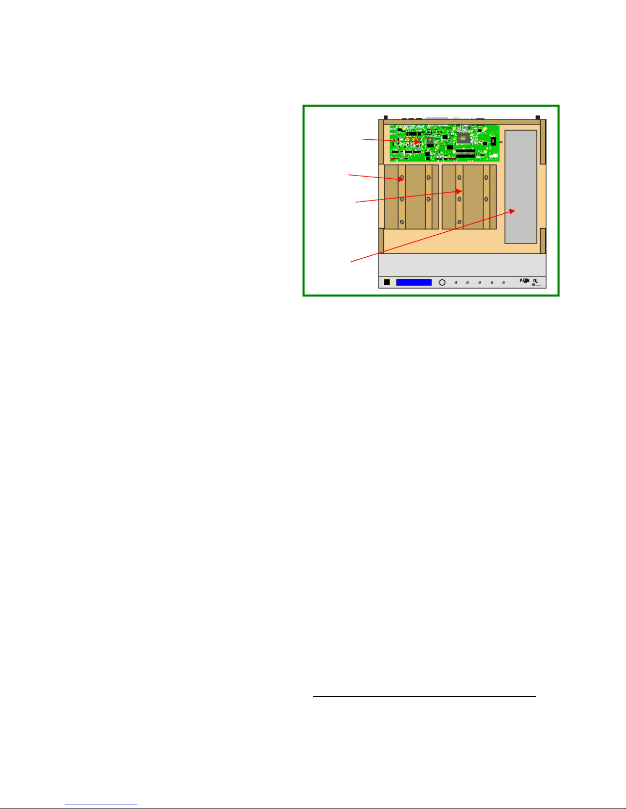
The Blade is a 1U high by 19” wide
rack-mountable unit containing two
SRM9000 sub-assemblies, a control
card, and a fan bulkhead which mates
with the angled front panel and MMI
card.
There is also provision for fitting a high
power amplifier or integrated power
supply option.
3.1 VENTILATION
In order to provide full-power
continuous operation in any
orientation and in a 1U envelope, the
Blade uses forced air-cooling. A pair
of fans draws air in from an air intake
located underneath the front lip of
the angled front panel. This air is
compressed by a baffle that directs
the airflow underneath the heatsink
of the SRM9000 sub assemblies. A
second pair of fans is used for the
high-power amplifier option if fitted.
Fans are located to maximise the cooling for the transmitting module. Air is exhausted
through a grilled area on the rear panel immediately below the electrical connectors.
Vent holes in the internal baffle allow a small amount of air to bleed diagonally through the
top section of the chassis to ensure that hot spots do not form on the component side of
the sub-assemblies.
The fans are mounted in a bulkhead located immediately behind the front panel. The front
panel, MMI board and fan bulkhead are separately assembled and removed from the unit
as sub-assemblies.
The fans, loudspeaker and indicator LEDs are all controlled from the MMI PCB that fits
into this sub-assembly. The fans are not only speed controlled to minimise noise and
wear, but their speed is also monitored to provide early warning of failure.
In normal operation, the fans are turned on to full speed to minimise any possibility of a
stall, the speed is then turned down based upon equipment temperature. Even if the
temperature is very low, fans are always kept running at a low speed. Temperature is
sensed from a Thermistor located on the underside of the control board. This Thermistor
protrudes into the airflow from the transmit PA module.
When installing the Blade it is important to ensure that adequate ventilation is provided for
each base station unit. A minimum free-area of 72cm2 is recommended per base station at
the inlet AND at the outlet. This should be increased if air has to be drawn through ducts
or has to be deflected around corners.
Receiver
Transmitter
Control Board
Figure 3.1 - Layout of the Blade with the top lid
removed
High-power
Amplifier or
Integrated PSU
Option
Page 12

PAGE 12 DESCRIPTION
Noise and dust build up can be reduced by keeping cabling and other obstructions out of
the main airflows.
There are no dust filters fitted in this product. If it is to be used in very dirty environments,
then additional steps should be taken to prevent ingress of dust as this will affect thermal
performance. Filters should only be used in external cabinets if they can be regularly
maintained.
3.2 SRM9000 SUB-ASSEMBLY
The RF performance of this product is derived from a pair of SRM9000 RF PCBs mounted
on a Heatsink sub-assembly that is designed to permit continuous operation at full power.
The sub-assembly also provides RF screening, so it is important that it is accurately
assembled and reassembled.
The sub-assembly has a plate attached to the rear edge with two quarter-turn fasteners for
rapid removal.
The unit is retained in the Blade chassis by the front edge of the Heatsink that inserts
underneath the fan baffle, the rear of the subassembly is held in place by the quick
release fasteners.
These units are electrically identical to SRM9000 and are also fully interchangeable in the
25W power group (the Transmit module is different for the 100W systems). Control is
provided via the 26-way ribbon connector. Power is supplied via the DB-15 connector and
RF signals are coupled to the BNC sockets with double-screened cables.
3.3 SPECIFICATIONS
3.3.1 General
Channel
Bandwidth
12.5kHz (11K0F3EJN), 20kHz (14K0F3EJN) or 25kHz (16K0F3EJN)
selectable per channel
Modulation
Freq. F3E (voice) pre-emphasised/flat, or FFSK data (1200 or
2400bps)
Frequency
Bands
E0: 66-88MHz. AC: 136-174MHz. K1: 174-208MHz.
KM: 208-245MHz. R0: 310-350MHz. R1: 335-375MHz.
TK: 400-450MHz. TU: 400-480MHz UW: 440-500MHz.
WR: 470-530MHz.
Stability
± 2.0ppm
Temperature
-25C to +55C Operating (Full Spec.) -40C to +80C Storage
Antenna
Connect
2 x 50Ω female N-type
Environmental
IP20 ingress protection, Humidity <95% non-condensing
Page 13
XFIN-BLADE-SM
DESCRIPTION PAGE 13
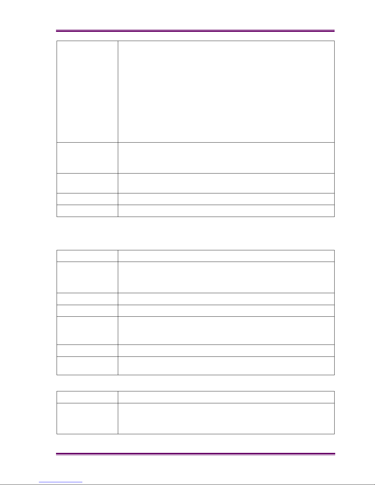
Inputs/Outputs
Serial interface with 1x audio connection (RJ45 – front panel)
2x line/audio (2/4-wire) connections with E&M signalling (2x RJ45
with internal shield)
Programmable facilities connector (37 way D-type)
2x RS232 serial connections (9 way D-type, RJ45 with internal
shield)
Ethernet IP interface (10/100 base-T magnetic RJ45 with external
shield)
USB connector (Type-B USB Socket)
PSTN connector (6/4 RJ-11 socket)
Power connector (5 Pin, 25 D-shell)
Type Approval
CE Type approvals to R&TTE Directive 1999/05/EC:
EN300-086 Radio, EN300-113 Data, EN301-489-05 EMC, EN300219 Signal, EN60950 Safety, TBR15, 17 and 21 Line
Dimensions
44mm(1U) High x 437mm Wide x 450mm Deep (Excluding cables
and ears)
(In Wall Mount)
125mm High x 465mm Wide x 470mm Deep
Weight
6.95 kg
3.3.2 Transmitter
25W
Transmit Power
1W to 25W in steps – 2 levels (high/low), selectable per channel
Tx Current
Consumption
Typical: 25W: 7A @13.6V (20°C)
Max: 25W: 10A @13.6V + 10.0A @27.3V (fans & audio on
maximum)
Duty Cycle
100%
Audio Distortion
<5% at 1kHz, 60% deviation
Audio
Frequency
Response
+1db to –3db of pre-emphasised 300 to 3000Hz on 25kHz channel,
300 to 2550Hz on 12.5kHz channel
Hum and Noise
>40db (12.5kHz), 45db (25kHz)
Transmit Rise
Time
<25ms
100W
Transmit Power
10W to 100W in steps, selectable per channel
Tx Current
Consumption
Typical: 100W: 5.7A @13.6V + 6.0A @27.3V (20°C)
Max: 100W: 8.85A @13.6V + 10.0A @27.3V (fans & audio on
maximum)
Page 14
PAGE 14 DESCRIPTION
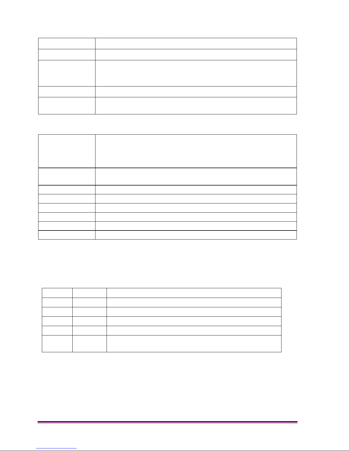
Duty Cycle
100%
Audio Distortion
<5% at 1kHz, 60% deviation
Audio
Frequency
Response
+1db to –3db of pre-emphasised 300 to 3000Hz on 25kHz channel,
300 to 2550Hz on 12.5kHz channel
Hum and Noise
>40db (12.5kHz), 45db (25kHz)
Transmit Rise
Time
<25ms
3.3.3 Receiver
Sensitivity
Voice: ≥12db SINAD for 0.3µV
pd
(typically >20db) for 25kHz channel.
Data: typical FFSK performance for <10
-2
BER (<20%MER):
0.3µV
pd
– 1200 baud in 12.5kHz & 1200/2400 baud in 25 kHz,
0.5µV
pd
– 2400 baud in 12.5kHz channel. [Ref: EN300-113-1:9.1]
Rx Current
Consumption
Typical: 1.0A (20°C)
Max: 1.55A (fans & audio on maximum)
Selectivity
>73db (25kHz), >63db (12.5kHz)
Intermodulation
>70db (ETSI method)
Audio Response
±3dB of de-emphasised 300 to 3000Hz with CTCSS
Audio Output
2W
rms
internal monitor speaker
Blocking
>95dB at ±1Mhz
Hum and Noise
>40dB (12.5kHz) – CCITT weighted
3.4 FRONT PANEL CONTROLS
3.4.1 LED Indicators
On the front of the Blade there are the following 5 LED indicators (from left to right):
Legend Colour Description
Power Green Indicates presence of 3.3V DC
Tx Red Indicates unit is keyed up
Rx Yellow Indicates RF signal received
CC Orange Control Channel Activity
Alm Red Alarm indicator – access LCD ‘alarms’ menu or connect
PC to diagnose
3.4.2 LCD
On the left side of the front panel is an LCD (Liquid Crystal Display) 2-by-20 Character
Display. It indicates channel (control/traffic) and network status (master/slave). It also
indicates volume level for the internal monitor speaker and presents a menu system. See
the LCD Menu Operation section later in the manual.
Page 15

XFIN-BLADE-SM
DESCRIPTION PAGE 15
3.4.3 Control Knob
The control knob is used in conjunction with the LCD Display to operate the menu system
and provide volume control.
Page 16
PAGE 16 DESCRIPTION
3.4.4 MMI RJ45 Connector
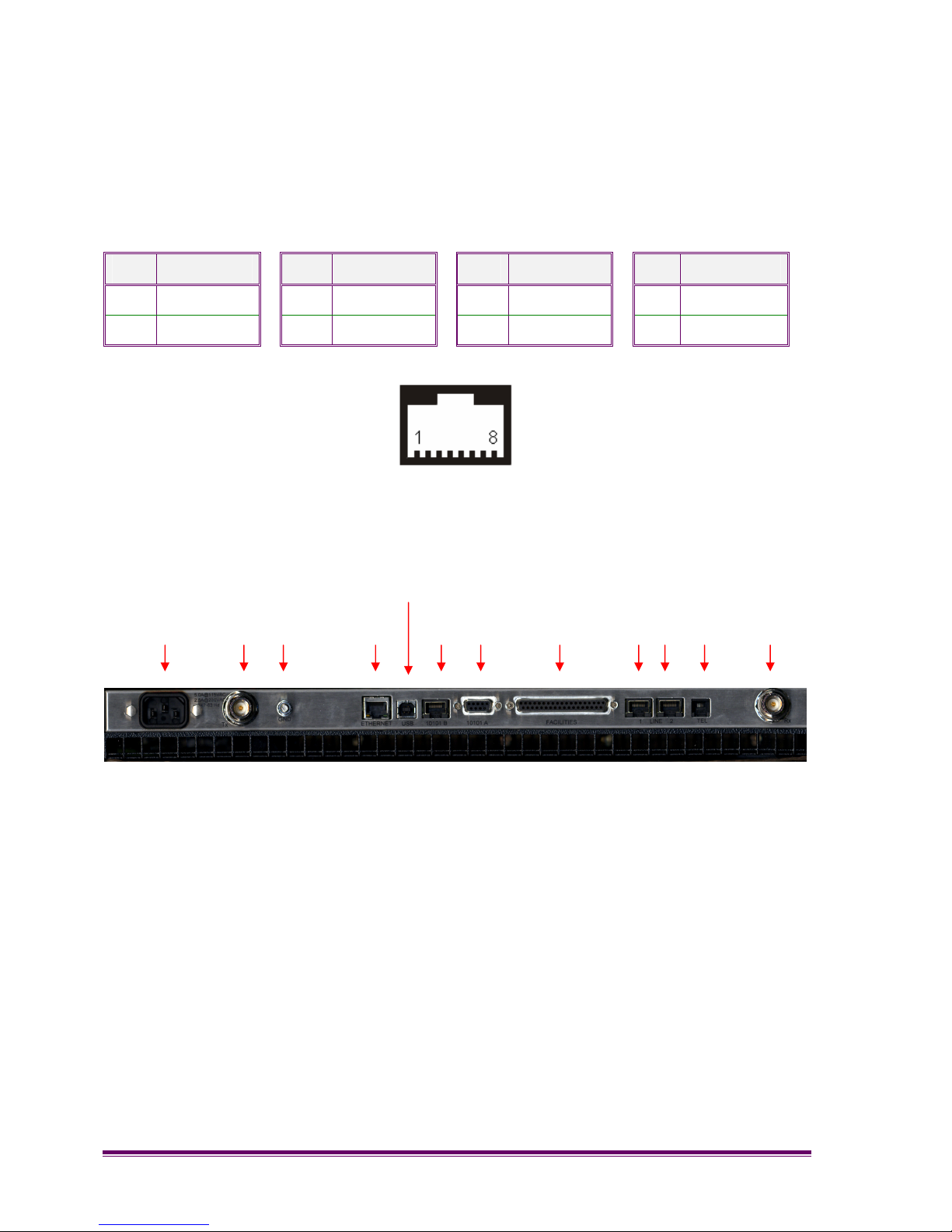
This is an RJ45 connector located on the left side of the angled front panel. It offers a
direct UART interface, a microphone input channel and an audio output channel. The
pinout is listed below (where for the purpose of this table, pin 1 is the left-most pin when
looking into the RJ45 socket).
Pin Function Pin Function Pin Function Pin Function
1 Tx-Data 3 N/C 5 +Vout 7 Gnd
2 Rx-Data
4 Mic Gnd
6 Audio Out 8 Audio In
3.5 REAR PANEL CONNECTORS
Figure 3.2 - Layout of the Xfin Blade rear panel
Tx Power GND Ethernet Serial Facilities
Line
1 2
PSTN Rx
USB
Page 17
XFIN-BLADE-SM
DESCRIPTION PAGE 17
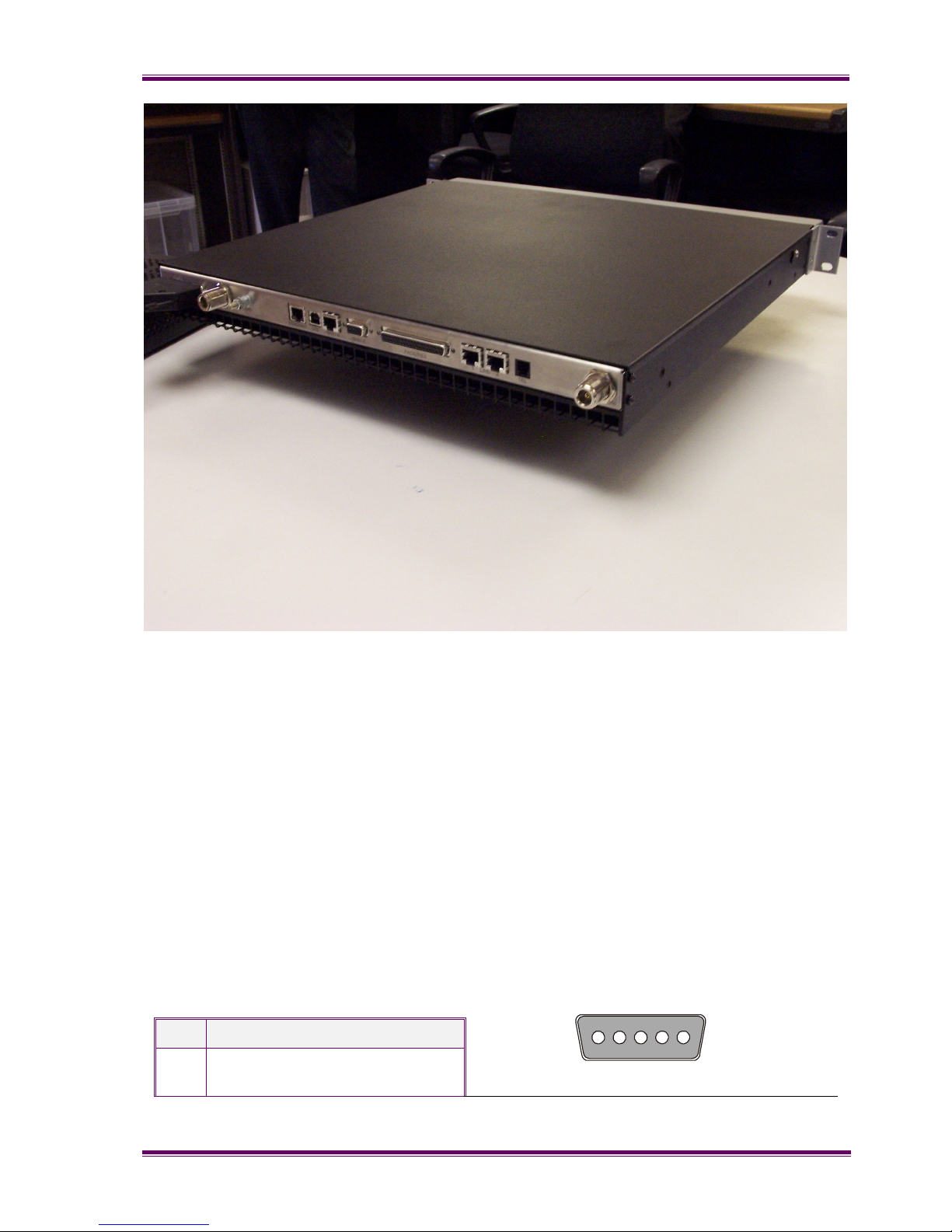
Figure 3.3 – View of the Xfin Blade rear panel.
3.5.1 Tx/Rx
The antenna connections on the Blade are provided with 50Ω female N-type sockets.
Mating connectors should be galvanically compatible with nickel outer and gold centre pin
to minimise passive inter-modulation.
A minimum of 85dB transmit-receive isolation should be provided by the antenna system
and associated filters.
It is recommended that a good quality flexible co-axial cable is used, e.g. with doublescreening braid and multi-strand copper inner.
3.5.2 Power
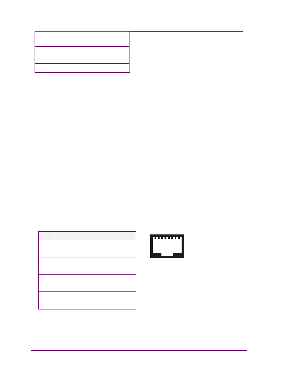
This is a D-type housing with 5 stud-pin locations. From left to right (looking at the rear
panel) they are:
Pin Description
1 Power amp (option). +24VDC
(nom)
1 5
Page 18
PAGE 18 DESCRIPTION
2 Power amp (option). DC
ground
3 Chassis Ground
4 +12VDC(nom) input
5 0VDC input
Notes: 12VDC nominal is normally supplied with 13.6VDC
for battery float charge reasons.
24VDC nominal is normally supplied with 27.3VDC
for battery float charge reasons.
3.5.3 Fuses
Fuse F1 on the fuse-board is a 2A quick-blow, 20 x 5mm component and protects the 12V
line to the MMI PCB.
Fuse F2 on the fuse-board is a 10A quick-blow, 20 x 5mm component and protects the
24V line to the Power Amplifier, if fitted
Fuse F5 on the Xfin Control Card is a 3.15A quick-blow, 20 x 5mm component and
protects the 12V line to the PCB.
In event of failure, the reason for the failure should be investigated prior to replacement.
The fuse should only be replaced with a correctly specified component.
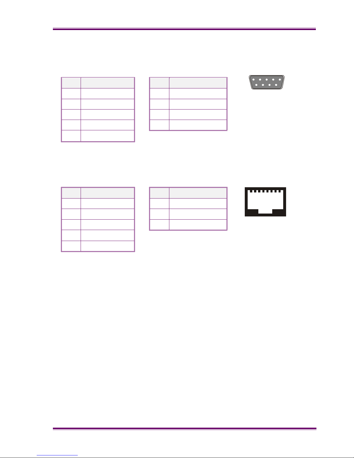
3.5.4 Ethernet
This is a 10/100 base-T RJ45 connection. This is a switch (not a NIC) configuration – care
should be taken to use the correct cable (crossover or straight-through) when connecting
to a network. The use of shielded cables is recommended, especially for VHF installations.
The two indicator LEDs, integrated into the connector, show 100Mbps bandwidth detection
and traffic activity. A third LED, on the Control Card shows if a connection is present.
Pin Description
1 Eth Rx-Data, balanced input 1
2 Eth Rx-Data, balanced input 2
3 Eth Tx-Data, balanced output 1
4 NC
5 NC
6 Eth Tx-Data, balanced output 2
7 NC
8 NC
1
8
Page 19
XFIN-BLADE-SM
DESCRIPTION PAGE 19
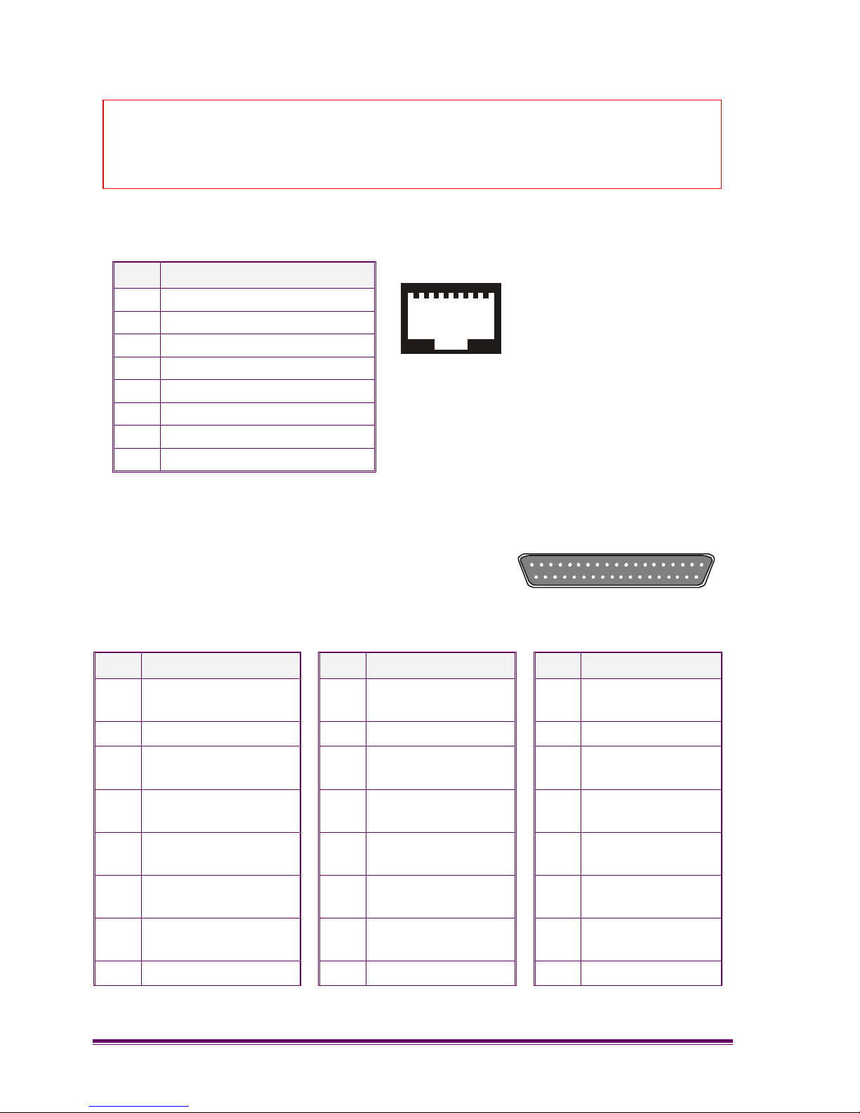
3.5.5 RS232 Serial (D-Sub)
This is a standard DB-9 female RS-232 socket with the following pins connected for DTE
operation:
Pin Description Pin Description
1 NC 6 NC
2 Tx Data, output 7 CTS, input
3 Rx Data, input 8 RTS, output
4 NC 9 NC
5 GND
3.5.6 RS232 Serial (RJ45)
This is a standard RJ45 socket with the following pins connected for DTE operation:
Pin Description Pin Description
1 NC 6 NC
2 Tx Data, output 7 CTS, input
3 Rx Data, input 8 RTS, output
4 NC
5 GND
3.5.7 USB Connector
The IXP420 processor's USB is integrated, USB 1.1-compliant and supports all standard
device requests issued by any USB host controller. It is an USB device-only controller.
The interface supports full-speed operation and 16 endpoints and includes an integrated
transceiver. There are six isochronous endpoints (three input and three output), one
control endpoint, three interrupt endpoints, six bulk endpoints (three input and three
output). The connector is a standard 4-pin socket (pin 1 is the bus voltage rail, 2 & 3 are
the positive and negative signals of the differential USB receiver/driver respectively and
pin 4 is ground).
Note: ensure that the current Blade software supports this interface before attempting to
use it
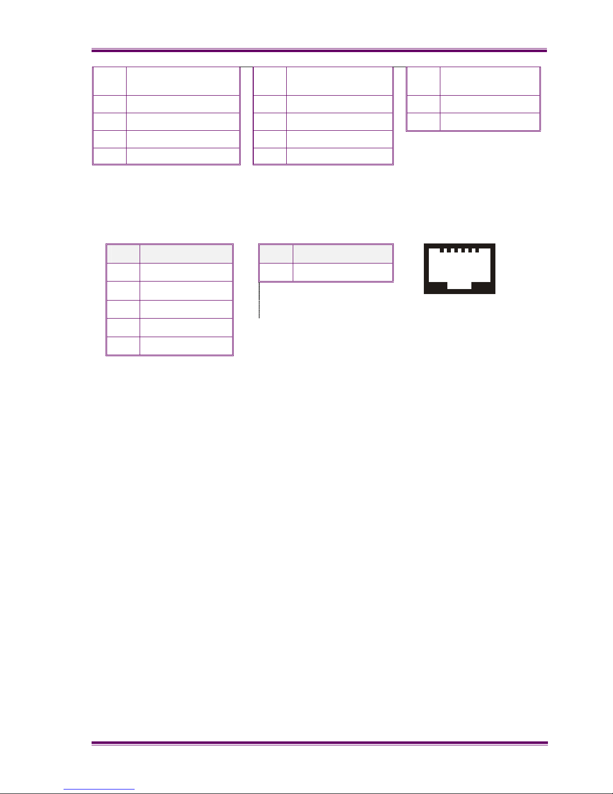
3.5.8 Line 1 & 2 (RJ45)
Each of these sockets provides a pair of barriered line audio connections via RJ45
connectors. Opto-isolated E&M signalling is also available on these connectors. A pair of
lines is provided so that the unit can support active line combining.
To provide DC Ground and Bias for E&M Signalling
1
6
5
9
1
8
Page 20
PAGE 20 DESCRIPTION
Where line barrier is not required, two fuses may be fitted in fuse-holders F3 and F4 of the
control PCB (20 x 5mm, 50mA) to provide DC ground and bias for E&M signalling.
Pin Description
1 E+
2 M3 4 wire Tx
4 4 wire Rx or 2 wire Tx/Rx
5 4 wire Rx or 2 wire Tx/Rx
6 4 wire Tx
7 M+
8 E-
3.5.9 Facilities
This 37-way D-type can be programmed for any
combination of digital inputs and outputs. Audio signals
are present on certain pins, these require an adapter
cable in order to re-route signals and become plug
compatible with certain products.
Pin Description Pin Description Pin Description
1 Tx+ line connection
A
14 CTCSS decode
defeat
27 I/O 5
2 0v 15 RSSI O/P 28 I/O 6
3 Rx+ line connection
A
16 Channel line C6
(MSB)
29 Talkthrough
command
4 Rx+ line connection
B
17 Channel line C4 30 Squelch defeat
command
5 Tx+ line connection
B
18 Channel line C2 31 I/O 7
6 Tx- line connection
B
19 Channel line C0
(LSB)
32 Aux Rx
7 I/O 2 20 Tx- line connection
A
33 I/O 8
8 I/O 4
21 Aux Tx
34 Analogue Out
Caution
When the following is performed, the line barrier is breached and the
equipment must NOT be connected to Public Networks.
1
8
1
20
19
37
Page 21
XFIN-BLADE-SM
DESCRIPTION PAGE 21
9 +13.6v unswitched 22
Rx- line connection
A
35 Channel line C5
10 Tx key command 23
Rx- line connection B
36 Channel line C3
11 Alarm 1 24 Squelch 37 Channel line C1
12 0v 25 I/O 1
13 Alarm 2
26 I/O 3
3.5.10 PSTN Port (RJ11)
This is a 6/4 RJ11 socket with the following pins connected for PSTN operation:
Pin Description Pin Description
1 NC 6 NC
2 NC
3 Tip (Snoop+)
4 Ring (Ring-)
5 NC
1
6
Page 22

Page 23
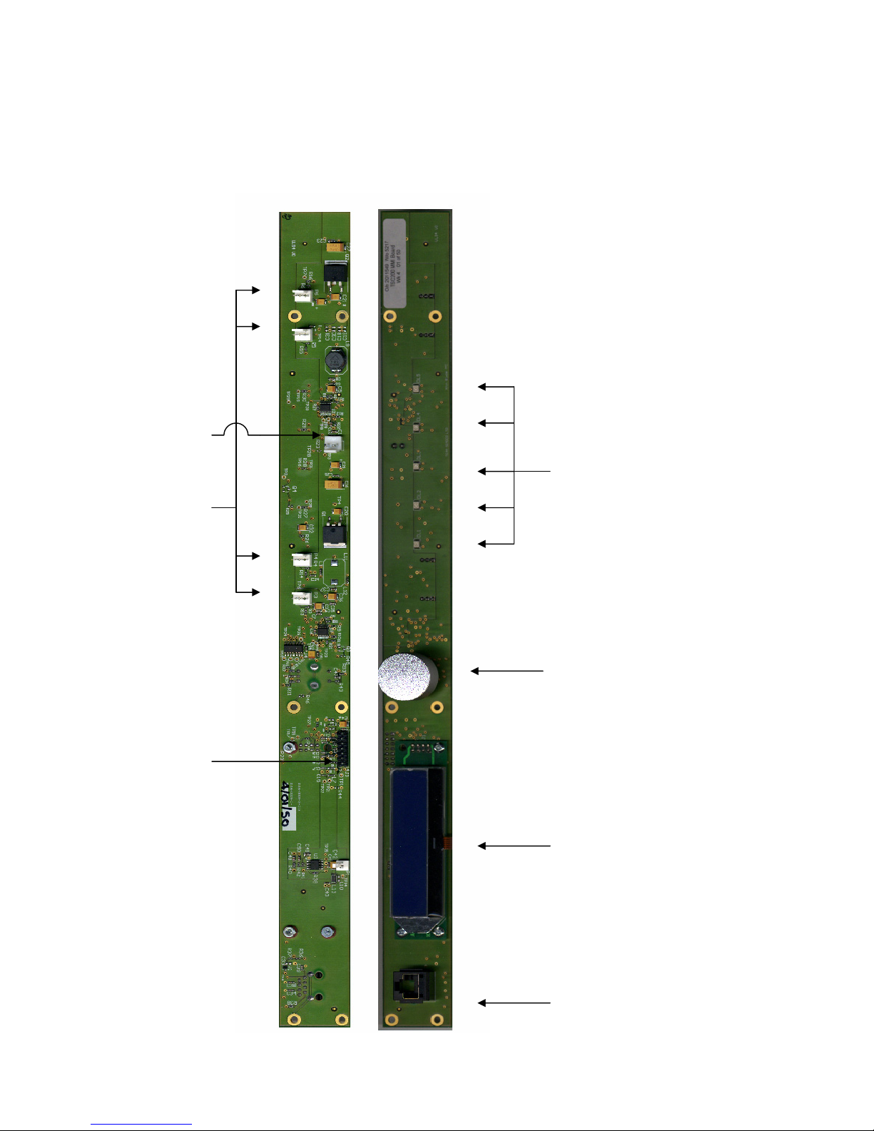
4 TECHNICAL DESCRIPTION
4.1 MMI BOARD
Figure 4.1 -
MMI Board
Layout
Control Knob
LCD Display
Handset Jack
LEDs
Fan
Connectors
MMI
Connector
Power
Connector
Page 24
PAGE 24 TECHNICAL DESCRIPTION
4.1.1 Description
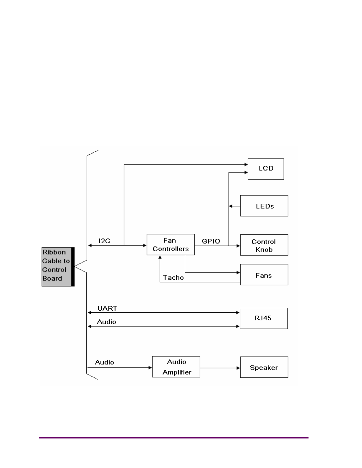
The purpose of the MMI board is to provide the Man Machine Interface between the
control card and the user.
The MMI board contains 5 LEDs for user diagnostics. It contains an LCD for displaying an
interactive menu, which is accessed via a control knob. An audio amplifier is provided to
drive a loud speaker at up to 2W, with volume adjustment via the control knob. An RJ45
interface for a serial port is also present.
The MMI board has a secondary function of providing the interface and drivers for the
fans.
Connection to the main control board is via a 14-way ribbon cable.
Figure 4.2 – Block Diagram of MMI Board
Page 25
XFIN-BLADE-SM
TECHNICAL DESCRIPTION PAGE 25
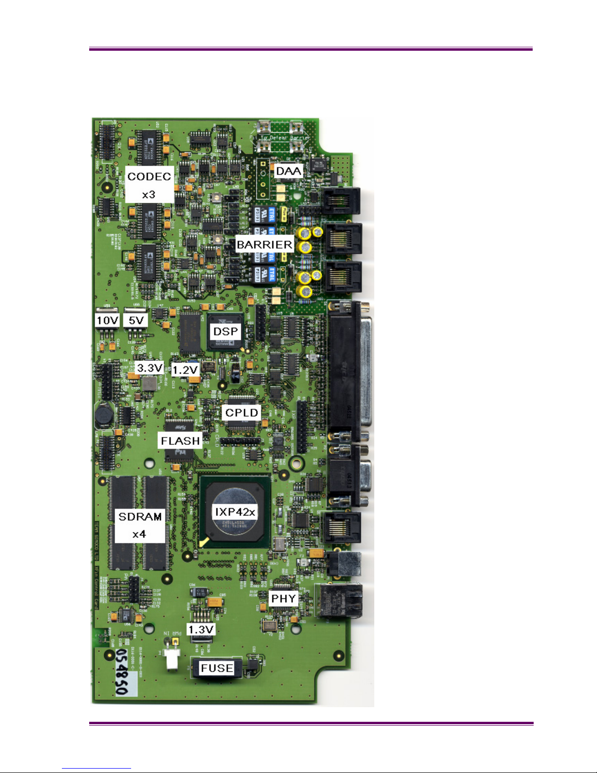
4.2 CONTROL BOARD
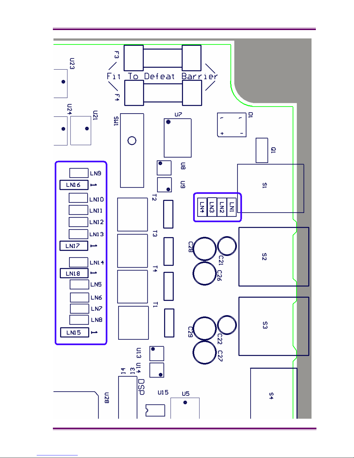
4.2.1 Circuit Board Layout
Figure 4.3 -
Control Board
Layout with Main
Sections Labelled
Page 26
PAGE 26 TECHNICAL DESCRIPTION
4.2.2 Circuit Description
See the Appendix for a more detailed block diagram representing the control card.
4.2.2.1 LEDs
LED DL1 indicates Ethernet connection (‘LINK’).
LED DL2 indicates the Flash device at U46 is being written to.
4.2.2.2 Test Points
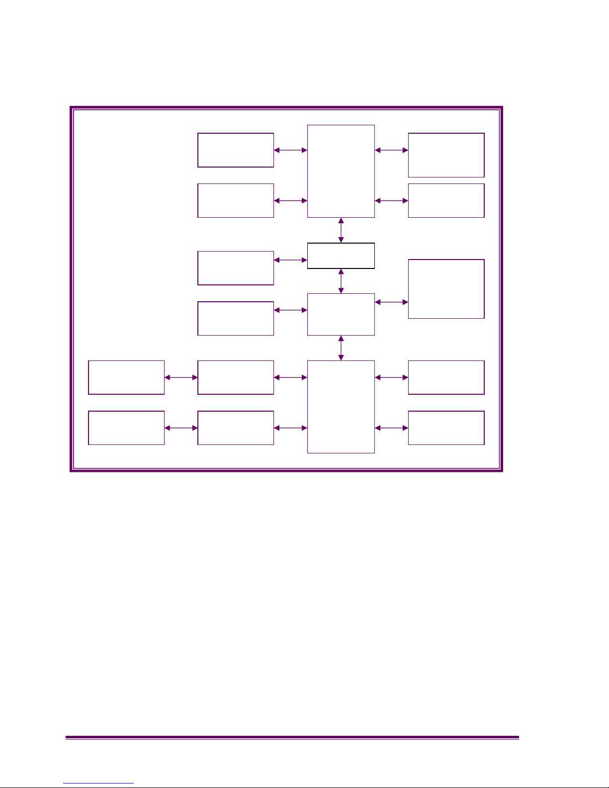
Figure 4.4 – Block Diagram of Control Board
IXP
DSP
CODECs
Analogue
I/O
Digital I/O
Ethernet
Control
Serial Port
Digital I/O
Serial
Control
Line Audio 1
Line Audio 2
Line
Barrier
Line
Barrier
BS Audio 1
BS Audio 2
SRM
Interface
CPLD
Page 27
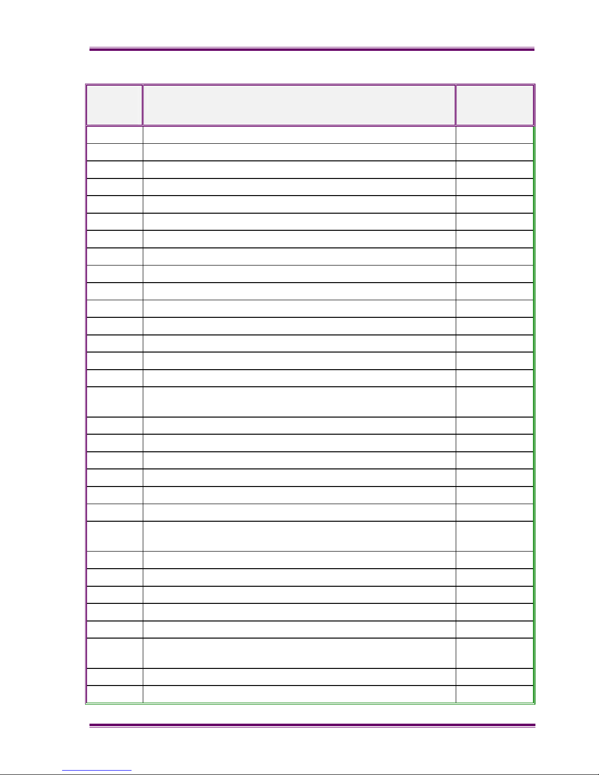
XFIN-BLADE-SM
TECHNICAL DESCRIPTION PAGE 27
Test
Point
Monitors
Signal Type
1 Active-Low INVALID Pin on RS232 chip (U1) 3.3V Digital
2 Active-Low INVALID Pin on RS232 chip (U2) 3.3V Digital
3 Transmit Centre-Tap on Magnetic RJ45 (P3) D.C.
4 Output 4 of Clock Driver (U12) Bank B Clock Signal
5 Inverted Output of Digital I/O Shift Register (U10) 3.3V Digital
6 Inverted Output of Digital I/O Shift Register (U17) 3.3V Digital
7 Inverted Output of Digital I/O Shift Register (U11) 3.3V Digital
8 Output 4 of Clock Driver (U12) Bank B Clock Signal
9 DSP PF10 3.3V Digital
10 IXP_IRQA output from CPLD (U22) 3.3V Digital
11 IXP_CLK_CPLD Signal to CPLD (U22) Clock Signal
12 IXP_IRQB output from CPLD (U22) 3.3V Digital
13 GPIO_IN4 Signal to CPLD (U22) 3.3V Digital
14 Feedback to Clock Driver (U12) Clock Signal
15 SPI_MISO signal to IXP GPIO(2) 3.3V Digital
16 TX_DATA signal for High Speed Serial Port 1 on the IXP
(U34)
3.3V Digital
17 RX_CLK signal for High Speed Serial Port 0 on the IXP (U34) 3.3V Digital
18 SPI_CS_ADC signal from IXP GPIO(9) 3.3V Digital
19 GPIO_IN7 Signal to CPLD (U22) 3.3V Digital
20 IXP_RD_N Signal to CPLD (U22) 3.3V Digital
21 I2C CLK (SCL) 3.3V Digital
22 SPI_CS_DS from IXP GPIO(3) 3.3V Digital
23 RX_DATA signal for High Speed Serial Port 1 on the IXP
(U34)
3.3V Digital
24 RTS for DSP Serial Port from DSP PF3 3.3V Digital
25 Off-Hook signal OH_N from DSP PF8 3.3V Digital
26 SPI_CS_DM 3.3V Digital
27 Spare I/O Pin CIO2 on CPLD (U22) 3.3V Digital
28 JTAG TDO Signal from CPLD (U22) 3.3V Digital
29 TX_FRAME signal for High Speed Serial Port 1 on the IXP
(U34)
3.3V Digital
30 TX_CLK signal for High Speed Serial Port 0 on the IXP (U34) 3.3V Digital
31 RX_CLK signal for High Speed Serial Port 1 on the IXP (U34) 3.3V Digital
Page 28
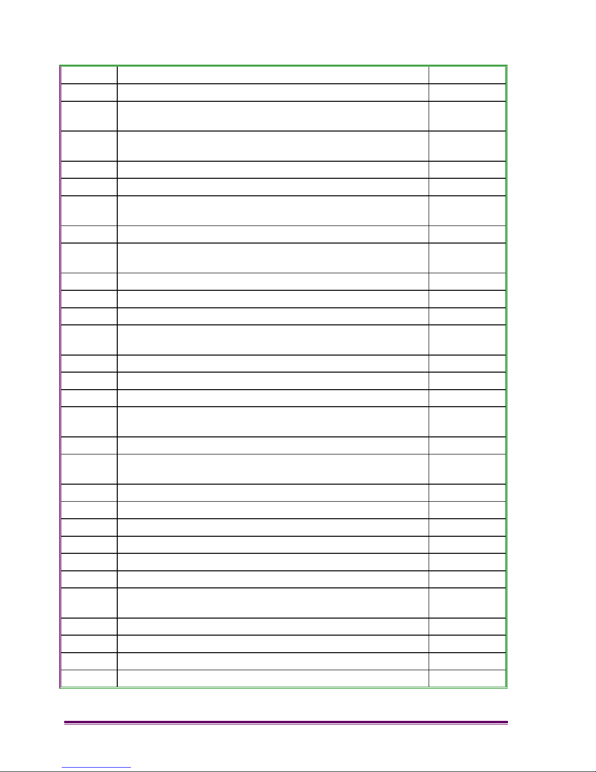
PAGE 28 TECHNICAL DESCRIPTION
32 PF1 on the DSP (U28) 3.3V Digital
33 I2C Data (SDA) 3.3V Digital
34 RX_FRAME signal for High Speed Serial Port 1 on the IXP
(U34)
3.3V Digital
35 Active-Low RING signal (indicating half-wave ringing detect
output signal) from PSTN interface (U7)
3.3V Digital
36 GPIO_IN6 Signal to CPLD (U22) 3.3V Digital
37 SPI_CS_DAC from IXP GPIO(10) 3.3V Digital
38 RX_FRAME signal for High Speed Serial Port 0 on the IXP
(U34)
3.3V Digital
39 TX_CLK signal for High Speed Serial Port 1 on the IXP (U34) 3.3V Digital
40 RX_DATA signal for High Speed Serial Port 0 on the IXP
(U34)
3.3V Digital
41 DSP Memory Select DSP_AMS3_N to CPLD (U22) 3.3V Digital
42 Spare I/O Pin CIO3 on CPLD (U22) 3.3V Digital
43 TDI JTAG Signal to CPLD (U22), connected to IXP GPIO(11) 3.3V Digital
44 TX_FRAME signal for High Speed Serial Port 0 on the IXP
(U34)
3.3V Digital
45 DSP_IRQA output from CPLD (U22) 3.3V Digital
46 GPIO_IN5 to CPLD (U22) 3.3V Digital
47 TMS JTAG Signal to CPLD (U22) 3.3V Digital
48 TX_DATA signal for High Speed Serial Port 0 on the IXP
(U34)
3.3V Digital
49 ENET0_INT_N to IXP GPIO(4) 3.3V Digital
50 Audio Output 1 from Codec C2 (U52) after passing through
the 1
st
Op-Amp stage
Audio Signal
51 DSP_IRQB output from CPLD (U22) 3.3V Digital
52 TCK JTAG Signal to CPLD (U22) 3.3V Digital
53 CPLDI_CS_N 3.3V Digital
54 DSP_IRQA output from CPLD (U22) 3.3V Digital
55 GPIO_IN3 to CPLD (U22) 3.3V Digital
56 GPIO_IN2 to CPLD (U22) 3.3V Digital
57 Audio Input 2 to Codec C2 (U52) prior to being converted
from single-ended to differential
Audio Signal
58 IXP Write Strobe IXP_WR_N 3.3V Digital
59 Active-Low Global Reset 3.3V Digital
60 Anti-Aliasing Filter Selector, generated by DSP PF11 3.3V Digital
61 SPI_MOSI generated by IXP GPIO12 3.3V Digital
Page 29
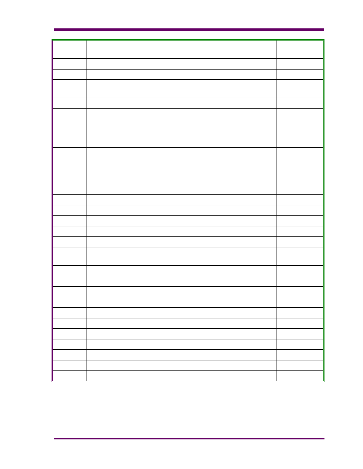
XFIN-BLADE-SM
TECHNICAL DESCRIPTION PAGE 29
62 Audio Input 1 to Codec C2 (U52) prior to being converted
from single-ended to differential
Audio Signal
63 SPI_CLK 3.3V Digital
64 5V Bias for 10V Op Amps D.C.
65 Audio Output 2 from Codec C2 (U52) after passing through
1st Op-Amp stage
Audio Signal
66 Analogue 3.3V A3V3 D.C.
67 Analogue Ground AGND D.C.
68 Analogue 2.5V Supply Rail (Bias for 5V Op Amps and ADC)
A2V5
D.C.
69 Codec Select Strobe CODSE generated by DSP PF4 3.3V Digital
70 Digital 5V supply rail (used by 3.3V Switched Mode Power
Supply) 5V0D
D.C.
71 Analogue 5V Supply Rail (used by ADC and 5V Op Amps)
A5V
D.C.
72 Codec Reset CODRST_N generated by DSP PF5 3.3V Digital
73 Digital Ground DGND D.C.
74 Pin 23 of P5 Rx Radio Header
75 Pin 21 of P5 Rx Radio Header
76 Pin 3 of P5 Rx Radio Header
77 I2C Data (I2C_SDA) 3.3V Digital
78 Analogue 2.5V Supply Rail (Bias for 5V Op Amps and ADC)
A2V5
D.C.
79 Digital Ground DGND D.C.
80 Pin 23 of P6 Tx Radio Header
81 Pin 21 of P6 Tx Radio Header
82 Pin 3 of P6 Tx Radio Header
83 TX_PTT inputted to DSP PF15 3.3V Digital
84 I2C CLK (SCL) 3.3V Digital
85 Pin 20 of P5 Rx Radio Header
86 3.3V Digital Voltage Supply 3V3 D.C.
87 RX_EXTOUT inputted to DSP PF9 3.3V Digital
88 Pin 6 of P6 Tx Radio Header
89 Digital Ground DGND D.C.
Page 30

PAGE 30 TECHNICAL DESCRIPTION
4.2.2.3 DSP
The DSP on the Xfin control card is a Blackfin device manufactured by Analog Devices; it
runs at speeds of up to 500 MHz. The DSP is responsible for all audio processing
including mixing, FFSK encoding/decoding, DTMF encoding/decoding, supervisory tone
generation, audio emphasis and speech processing for VOIP between Blades.
Booting
The DSP downloads the application code from the IXP Network Processor at start up and
runs the software entirely in internal memory.
RS232 Serial Interface (Rear RJ-45)
The rear of the Blade contains a standard RJ-45 Serial connection in order that an
engineer may connect a PC to the DSP via an RJ-45 to DB-9 cable. Debug commands
may then be issued to the DSP for diagnostic information.
CPLD Interface
Communications between the IXP Network Processor and the DSP are performed by
connecting the data bus on the IXP to the host interface (Lattice LC256V-75T100 CPLD)
connecting to the DSP. The IXP writes to the host interface, triggering a DMA on the DSP
to copy the data to a buffer. After a packet has been sent, the DMA on the DSP copies
data from an outgoing buffer to the host interface port that is read by the IXP. This enables
high-speed communications without impacting the performance of the DSP.
Page 31

XFIN-BLADE-SM
TECHNICAL DESCRIPTION PAGE 31
4.2.2.4 Power
The control board requires a 12V 2000ma supply. Linear regulators are provided to reduce
the input voltage down to 10V and 5V for the audio circuits. The input voltage supply is
also regulated down to 3.3V for the digital logic via a switched mode power supply. The
1.3V supply for the IXP processor core is generated by a regulator off the 3.3V rail. The
1.2V supply for the DSP core is generated by a diode (controlled by the DSP) off the 3.3V
rail.
4.2.2.5 IXP
Description
The main processor is an IXP42x processor manufactured by INTEL. It consists of a
central ARM based processor supported by separate network processor engines for
supporting the Ethernet and USB ports. The IXP runs the application code under
MontaVista Linux. The application code consists of Trunked Site Control, Inter-Blade
Communications, Site Configuration, Fan Control and the LCD menu system.
The network processor also provides support to the DSP. The IXP is connected to
external flash memory that stores the IXP software. Reset of the IXP is performed reset
circuitry monitoring voltage supplies.
Watchdog
The IXP processor has its own internal watchdog.
Fan Control
The IXP performs fan control via Maxim Fan Regulator devices, monitoring the
temperature of the airflow from the transmitter module using a thermistor (RT1). If the
temperature is too high or low, the speed of the fans is adjusted accordingly. Fans are not
allowed to stop during normal operation. Each fan generates a tachometer output allowing
software to detect a fan failure or potential failure by monitoring fan speed. If one fan fails
the speed of the second fan will be increased to compensate.
Analogue Outputs
Two analogue outputs are provided by a dual-channel Digital to Analogue Converter
(U41). They provide analogue outputs to the Facilities Connector to output, for example,
the RSSI level.
Analogue Inputs
The ADC (U56) has eight analogue inputs available, which are currently used to provide
voltage monitoring of the thermistor and the 12V unregulated supply, receive inputs from
the PA header and provide feedback of the analogue outputs.
Digital I/O
A set of shift registers (U10, U11, U15, U16 and U17) is controlled by the IXP via the
CPLD to provide digital I/O to the Facilities Connector as well as internal controls.
Ethernet interface
Page 32

PAGE 32 TECHNICAL DESCRIPTION
The IXP controls an LXT971 PHY chip (U20) that provides a 10/100 Base-T Ethernet
interface. The PHY is connected to an RJ-45 socket with built-in magnetics; the socket
also presents two external LEDs which are configured to indicate activity and 10/100
status.
RS232 Serial Interface (DB-9)
The rear of the Blade contains a standard 9-way Serial connection in order that a straight
through cable may be used to connect a PC to the IXP.
UART Serial Interfaces (Front Panel RJ-45)
The IXP presents a serial port interface to the RJ-45 port in the front panel.
4.2.2.6 CoDec
Audio received from either or both of the line ports and the PSTN interface is fed into a
chain of 3x AD73322L codecs (U52, U53 and U54) that is connected to the DSP via its
SPORT (Serial PORT) interface serial link.
The DSP performs audio signalling to the line equipment or patches the audio to the radio
module.
Handset audio is fed via a codec (U53) into the DSP allowing it to be mixed to line or the
radio modules under software control. Audio is also fed to the speaker on the front panel.
The codec contains built-in analogue gain adjustment under software control.
4.2.2.7 Audio Interface
General
External audio equipment is connected to either of the two independent audio ports which
are presented barriered on the RJ45 connectors, and un-barriered on the 37-way Facilities
Connector.
Two and Four Wire
The barriered connections are link selectable as either two or four wire. In two-wire mode
the balance of the hybrid can be set manually by moving LN18 (LN16 for port 2) to
position 2-3. If a test tone is generated to line, the reflected audio can be monitored on
TP57 (TP62 for port 2) and variable resistor R128 (R135 for port 2) can be adjusted to
give the minimum level.
At the time of configuration, the audio levels of the line ports must be set for optimal
performance. In line-to-air mode, it must be possible for a -10dBm signal to generate a
2.5kHz (full-scale) deviation. In loopback mode, an undistorted signal up to -10dBm should
be re-outputted with unity gain; this can be configured by inputting a -14.4dBm signal
(equivalent to 1.5kHz/60% deviation over air) into the line port and altering the gain level
until an equivalent -14.4dBm signal is seen at the output.
E & M
The control board contains opto-isolated digital inputs (U9, U14) and outputs (U8, U13). In
order to support local connections where an external bias voltage is not present, Fuse-
Page 33
XFIN-BLADE-SM
TECHNICAL DESCRIPTION PAGE 33
links F3 and F4 can be fitted to provide bias volts. This allows the unit to use DC
signalling.
4.2.2.8 PSTN Interface
A Clare DAA chip (U7) provides a PSTN interface. An audio channel links the telephone
port to a codec (U54).
At the time of configuration, the audio levels of the PSTN interface should be set for
optimal transmission and reception.
PSTN Interface Specifications:
Isolation
Characteristics
3000 Vrms rated isolation voltage; 2000V/µs rated surge rise time.
Continuous
Output Current
130 mA (max where Rzdc = 8.2Ω).
Ringing Signal
Detect Level
5 Vrms (min for 68Hz applied to tip and ring); 28 Vrms (min for 15Hz
applied across tip and ring).
Frequency
Response
30 to 4000Hz (166Hz to 4000Hz for Snoop Circuit).
Ringer
Equivalence
0.01B REN.
Return Loss
26 dB (typical, into 600Ω at 1800Hz).
Insertion Loss
-0.4dB to 0.4dB (Tx and Rx, 30 to 4000Hz).
Tx/Rx Level
2.2Vp-p (max) for a single-tone sine wave.
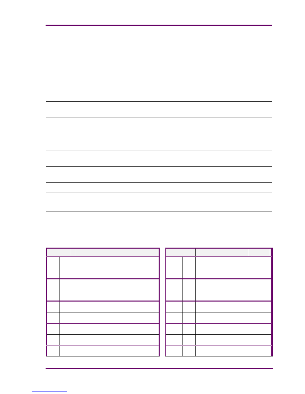
4.2.3 Links
For Fuse Links F3 and F4, see E & M above.
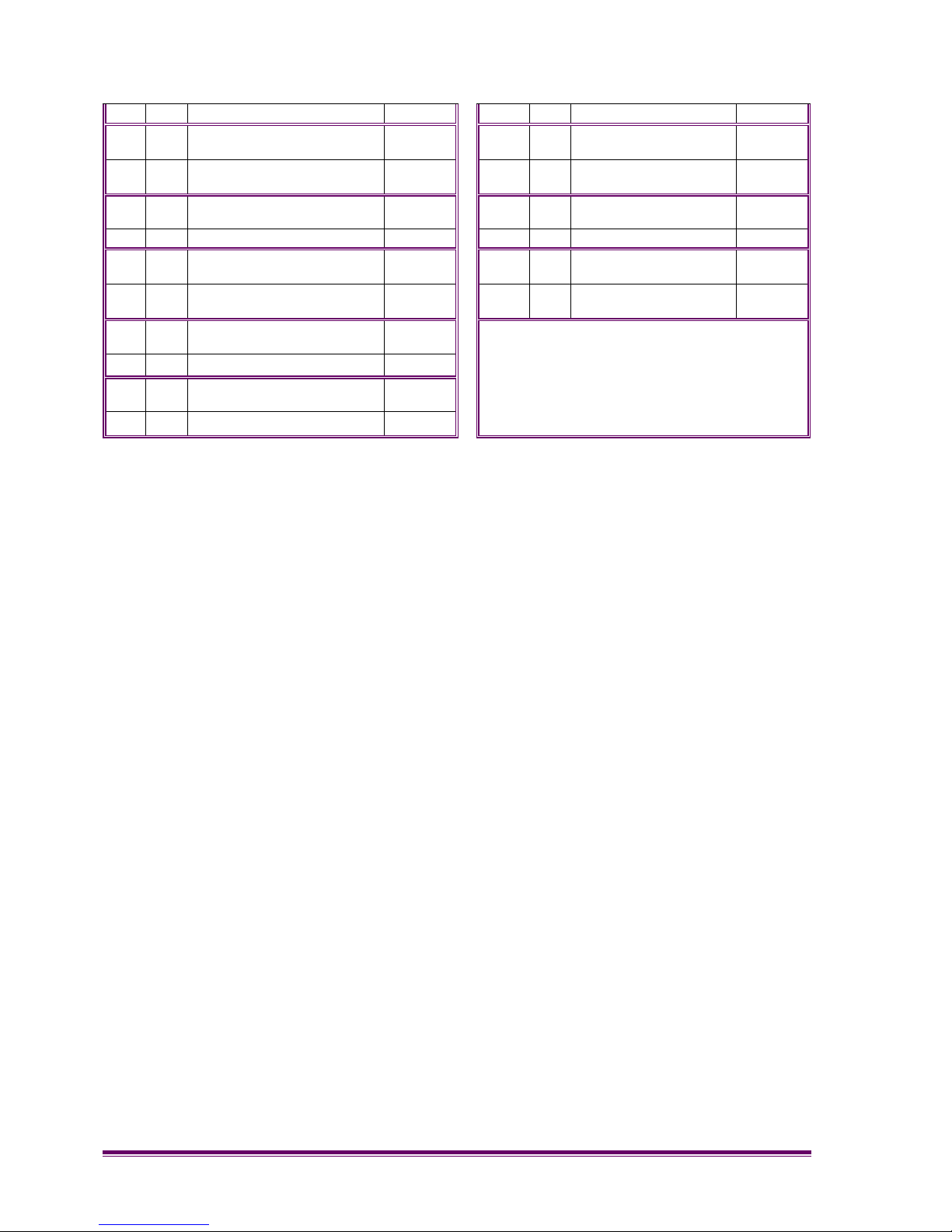
Link Remarks
Default
Link Remarks
Default
LN1 In Line 2 M-Wire bias GND -
requires F3 fit
LN11 In Line 2 Two-Wire 600R
Impedance select
Out No bias - barrier is not
breached
Out
LN2 In Line 1 M-Wire bias GND -
requires F3 fit
LN12 In Line 2 UK Complex
Impedance select
Out No bias - barrier is not
breached
Out
LN3 In Line 2 E-Wire +V Bias (input
supply volts) - requires F4 fit
LN13 In Line 2 Four-Wire RX
Impedance Enable
Out No bias - barrier is not
breached
Out Line 2 Two-Wire
LN4 In Line 1 E-Wire +V Bias (input
supply volts) - requires F4 fit
LN14 In Line 2 Complex Imped.
Hybrid Balance
Out No bias - barrier is not
breached
Out
LN5 In Capacitor link for Line 1 UK
Complex Impedance Select
LN15 1 - 2 Line 1 Four-Wire Mode
Page 34
PAGE 34 TECHNICAL DESCRIPTION
Out
2 - 3 Line 1 Two-Wire Mode
LN6 In Line 1 Four-Wire RX
Impedance Enable
LN16 1 - 2 Line 2 Two-Wire 600R
Imped. Hybrid Balance
Out Line 1 Two-Wire
2 - 3 Line 2 Adjustable Hybrid
Balance
LN7 In Line 1 UK Complex
Impedance Select
LN17 1 - 2 Line 2 Four-Wire Mode
Out
2 - 3 Line 2 Two-Wire Mode
LN8 In Line 1 Two-Wire 600R
Impedance select
LN18 1 - 2 Line 1 Two-Wire 600R
Imped. Hybrid Balance
Out
2 - 3 Line 1 Adjustable Hybrid
Balance
LN9 In Line 2 Complex Impedance
Hybrid Balance
Out
Note: Unless specifically ordered otherwise, the
Control Board is supplied in the default configuration
shown in this table.
N10 In Capacitor link for Line 2 UK
Complex Impedance Select
Out
Page 35
XFIN-BLADE-SM
TECHNICAL DESCRIPTION PAGE 35
Page 36

PAGE 36 TECHNICAL DESCRIPTION
4.3 RECEIVER AND TRANSMITTER MODULES
4.3.1 Frequency Bands
The Blade is supplied with a matched pair of radio sub-assemblies fitted.
The designated frequency bands are:
66 - 88 MHz E0 Band 335 - 375 MHz R1 Band
136 - 174 MHz AC Band 400 - 450 MHz TK Band
174 - 208 MHz K1 Band 400 - 480 MHz TU Band
208 - 245 MHz KM Band 440 - 500 MHz UW Band
310 - 350 MHz R0 Band 470 - 530 MHz WR Band
The following text refers to the components and circuits within the RF sub-assemblies
only. For additional information, refer to the SRM9000 Service Manual [1].
The Rx and Tx Modules are equivalent and interchangeable for a given power
classification (25W or 100W). They are connected to the Control Board via a 26-way
Ribbon Cable that carries analogue audio, digital audio and control signals.
Power connections are made via a 15-way, D-type connector and RF connections are
made via BNC sockets. RF connections are taken to the rear of the Blade via doublescreened cables terminated with female N-types.
4.3.2 Receiver
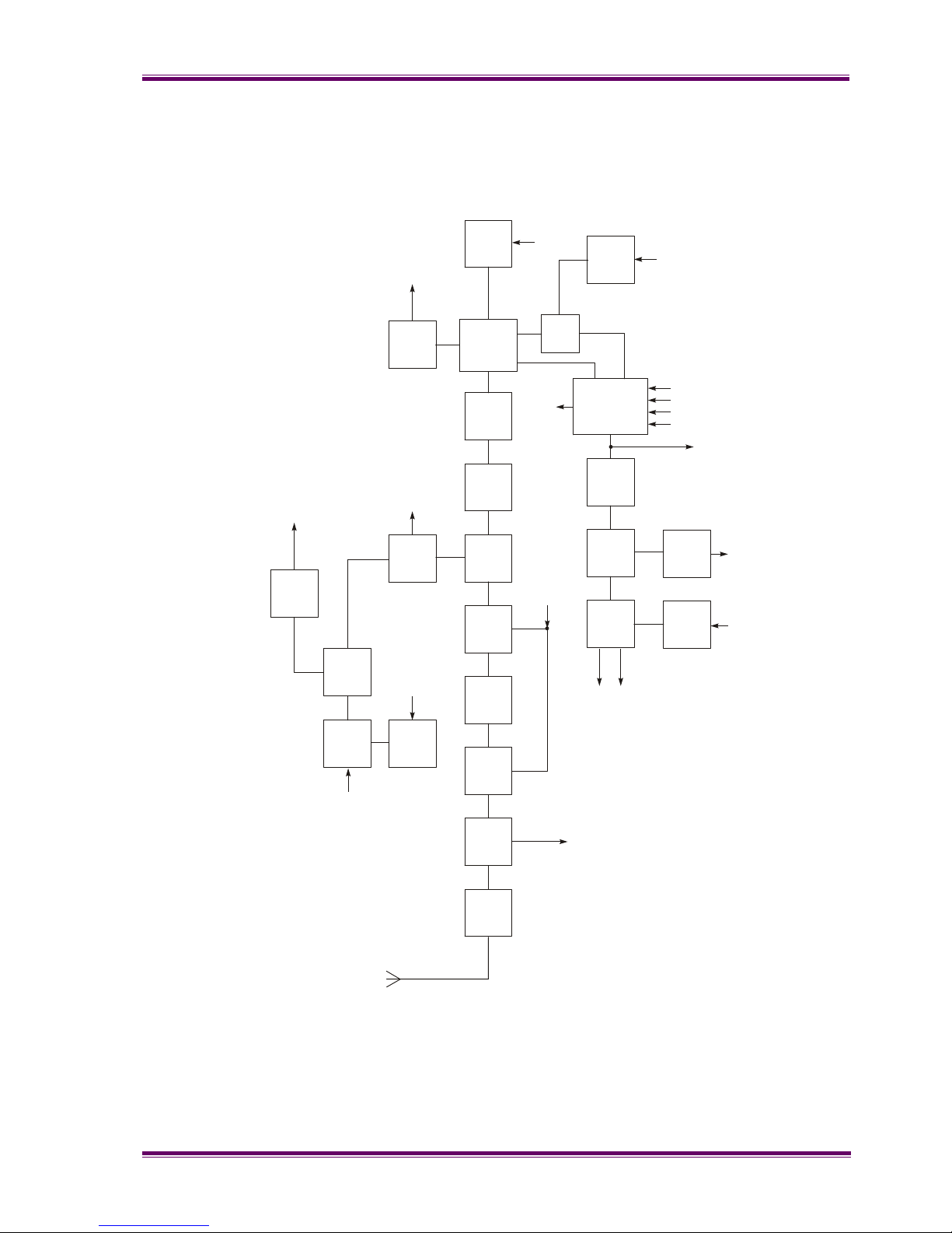
Refer to Figure 3.5.
4.3.2.1 Front-end Filters and Rx Front-end Amplifier
The receiver input signal from the antenna passes through the antenna filter comprising
L10, L11, L12 and associated tuning capacitors. With a transceiver module in receive
mode, diodes D3, D4 and D5 in the antenna switch are reverse biased allowing the
receiver input signal to be coupled through to the front-end with minimal loss. The overall
insertion loss of the antenna filter and switch is approximately 0.8dB.
Front-end selectivity is provided by varactor tuned bandpass filters at the input and output
of the RF amplifier.
Front-end tuning voltages are derived from the alignment data stored in the radio. The
DSP processes this data to optimise front-end tuning relative to the programmed channel
frequencies that may be changed at any time without re-aligning the radio.
To achieve the required varactor tuning range an arrangement of positive and negative
bias power supplies is used to provide a total bias across the varactors of up to 14.0VDC.
A fixed 2.5V positive bias derived from the 5.0V supply and voltage divider R425/426 is
applied to the cathodes of the varactor diodes. The negative bias supply originates at the
DSP/FPGA as a composite digital tuning signal (FE TUNE) containing the data for the four
front-end tuning values TUNE 1 to 4 for the particular channel frequency selected. The
level is dependent on channel frequency and tuning and varies between +0.1 and +3.0V.
This signal then passes through buffer U901A and level translator Q900 to Q903 where it
is converted to a high level (-0.5 to -11.5V) negative equivalent of the original signal.
Page 37
XFIN-BLADE-SM
TECHNICAL DESCRIPTION PAGE 37
The -12.0V rail of the level translator is generated by U300B/C with D304 to D306
providing the required voltage multiplier effect. The high level negative signal is then split
into the four individual front-end negative DC values under software control by multiplexer
U902 and associated storage capacitors C904 to C907 before being applied to the anodes
of the front-end tuning varactors.
Figure 3.5 - VHF/UHF Receiver Block Diagram
9
0
0
0
_
1
6
A
n
t
e
n
n
a
S
w
i
t
c
h
D
3
,
D
4
&
D
5
A
n
t
e
n
n
a
F
i
l
t
e
r
L
1
0
,
L
1
1
&
L
1
2
9
0
M
H
z
L
.
O
.
Q
4
0
2
R
x
V
C
O
Q
6
0
0
R
x
V
C
O
S
w
i
t
c
h
Q
6
0
1
V
C
O
B
u
f
f
e
r
Q
6
0
4
/
6
0
5
S
y
n
t
h
e
s
i
s
e
r
B
u
f
f
e
r
Q
6
0
7
t
o
U
7
0
1
T
o
T
x
B
u
f
f
e
r
t
o
U
7
0
1
T
o
T
x
P
A
C
P
P
V
C
O
C
o
n
t
r
o
l
V
o
l
t
s
R
x
P
S
U
T
x
/
R
x
S
w
i
t
c
h
D
6
1
0
/
6
1
1
R
x
/
T
x
A
F
S
w
i
t
c
h
U
1
0
3
B
M
i
c
A
m
p
Q
8
1
2
B
a
n
d
p
a
s
s
F
i
l
t
e
r
R
F
A
m
p
Q
4
0
0
B
a
n
d
P
a
s
s
F
i
l
t
e
r
M
i
x
e
r
T
4
0
0
I
F
A
m
p
Q
4
0
1
S
p
e
a
k
e
r
A
m
p
U
5
S
p
k
r
S
w
i
t
c
h
Q
8
1
0
/
8
1
1
/
8
1
3
4
-
P
o
l
e
4
5
M
H
z
F
i
l
t
e
r
s
Z
4
0
1
/
4
0
2
A
F
A
m
p
U
8
0
3
A
u
x
A
F
O
/
P
A
m
p
U
8
0
3
I
Q
D
e
m
o
d
u
l
a
t
o
r
U
4
0
1
R
x
A
F
S
w
i
t
c
h
U
1
0
3
C
A
G
C
B
u
f
f
e
r
U
9
0
1
B
A
D
C
/
D
A
C
C
O
D
E
C
U
8
0
0
F
r
o
m
M
u
l
t
i
p
l
e
x
e
r
U
9
0
2
T
u
n
e
1
,
2
,
3
&
4
Q
I
A
F
C
/
R
e
f
O
S
C
/
M
O
D
A
u
d
i
o
I
n
F
r
o
m
M
i
c
A
u
d
i
o
o
r
O
p
t
i
o
n
A
u
d
i
o
F
r
o
m
M
u
l
t
i
p
l
e
x
e
r
U
9
0
2
F
r
o
m
F
P
G
A
/
D
S
P
A
U
D
O
u
t
S
P
K
R
O
N
S
P
K
R
O
U
T
1
S
P
K
R
O
U
T
2
T
X
M
O
D
1
T
o
T
X
V
C
O
S
Y
N
T
H
A
U
X
C
P
Page 38

PAGE 38 TECHNICAL DESCRIPTION
The RF front-end amplifier stage comprises a low-noise transistor amplifier (Q400), which
is compensated to maintain good linearity across the required frequency bands and
temperature range. This provides excellent intermodulation and blocking performance
across the full operating range. The gain of this stage is typically 17dB for both UHF and
VHF versions.
4.3.2.2 First Mixer and IF Section
The output of the last front-end bandpass filter is coupled into single balanced mixer
T400/D413 which converts the RF signal to an IF frequency of 45MHz.
The local oscillator injection level is typically +8dBm at T400 pin 1 with low side injection
used for UHF and high side for VHF. Following the mixer is IF amplifier Q401 which
provides approximately 15dB of gain and in association with its output circuitry presents
the required load conditions to the 4 pole 45MHz crystal filter Z401/402.
4.3.2.3 Quadrature Demodulator
Additional IF gain of approximately 30dB occurs at U401, which is a dedicated IF AGC
amplifier/Quadrature, Demodulator configured for single-ended input and output operation.
The AGC voltage for U401 is derived from the RSSI function of the DSP via AUX CTL and
multiplexer U902. The onset of AGC operation occurs when RF input signal levels at the
antenna exceeds -90dBm. Conversion of the 45MHz IF signal to I and Q baseband signals
is carried out by the demodulator section of U401. The 90MHz local oscillator signal is
generated by VCO Q402 which is phase locked by the auxiliary PLL output of U701 via
feedback signal AUX LO2.
4.3.2.4 Receiver Audio Processing
All receiver audio processing and filtering functions are performed by the CODEC U800
under the control of the DSP.
The receiver I and Q analogue baseband signals are converted to digital signals by the
CODEC ADC before being applied to a series of digital filters which provide the final stage
of adjacent channel filtering, high pass and low pass filtering and mute noise processing
for narrow and wideband operation. The processed signals are then converted to
analogue audio signals by the CODEC DAC and are applied to conventional audio
amplifiers U803A/B and the speaker amplifier U5.
The speaker circuits are not used in the Blade. The carrier and signalling mute functions
are performed by Q810/811/813 under DSP control with additional receiver muting to
U803B being applied by U103C when the mobile is in transmit mode.
Flat audio (20Hz – 5.8kHz) is provided to S1-6 via amplifier U803A. De-emphasis is
performed on the Control Board.
Software functions are used to filter off signals below 300Hz and above 3kHz.
4.3.3 Transmitter
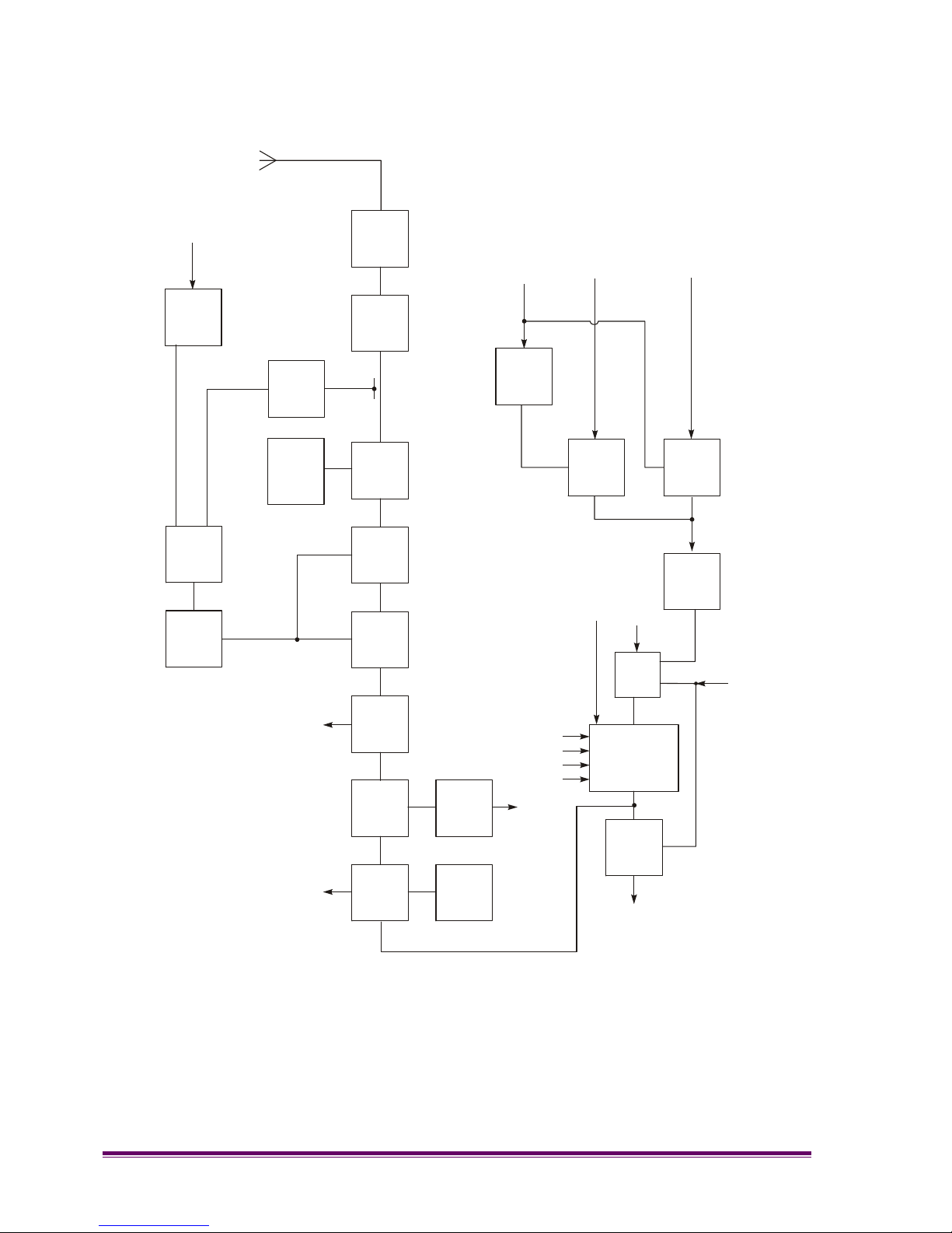
Refer to Figure 3.6.
Page 39

XFIN-BLADE-SM
TECHNICAL DESCRIPTION PAGE 39
4.3.3.1 Drivers and PA Stages
The RF output level from the VCO buffer Q604 is typically +5dBm (UHF) and +8dBm
(VHF). TX buffer Q606 increases this level by approximately 3dB (UHF) and 11dB (VHF)
and also provides additional VCO isolation.
The following section of the TX buffer Q612 is controlled by the transmitter power control
loop and Q609. Q609 is normally saturated in transmit mode so there is no minimum gain
control applied to this stage. The gain of Q612 is typically 10dB (UHF) and 15dB (VHF) but
the output level is reduced by input and output resistive attenuators to limit the PA driver
input level to typically +20dBm. The gain of PA driver Q12 is controlled by the power
control loop to ensure that transmitter output power remains within defined limits. The PA
driver output level is typically +25dBm.
PA module U2 utilises three stages (UHF) and two stages (VHF) to achieve the required
final RF output power level of +44dBm (25 watts). Power output settings are derived from
alignment data stored in flash memory during the initial factory alignment. The DSP
processes this data to optimise the power output level relative to the programmed channel
frequencies which may be changed at any time without retuning the radio.
An active filter comprising Q14, 17,18 and 19 provides isolation to minimise power supply
noise at the PA. This is achieved by maintaining a voltage differential of approximately 1V
across Q14 and indirectly filtering its gate voltage. Q14 is switched on only during transmit
via R523 to minimise receiver power requirements.
Page 40
PAGE 40 TECHNICAL DESCRIPTION
Figure 3.6 - VHF/UHF Transmitter Block Diagram
9
0
0
0
_
1
7
T
x
/
R
x
S
w
i
t
c
h
D
6
1
0
/
6
1
1
T
x
V
C
O
Q
6
0
2
T
x
V
C
O
S
w
i
t
c
h
Q
6
0
3
T
x
B
u
f
f
e
r
/
A
m
p
Q
6
0
6
/
6
0
9
/
6
1
2
P
o
w
e
r
C
o
n
t
r
o
l
Q
3
/
1
0
V
C
O
B
u
f
f
e
r
Q
6
0
4
/
6
0
5
S
y
n
t
h
e
s
i
s
e
r
B
u
f
f
e
r
Q
6
0
7
T
x
P
A
D
r
i
v
e
r
Q
1
2
C
o
m
p
a
r
a
t
o
r
U
3
A
Q
1
5
/
1
6
T
X
P
A
U
2
T
x
P
A
F
i
l
t
e
r
/
S
w
i
t
c
h
Q
1
4
/
1
7
/
1
8
/
1
9
P
o
w
e
r
C
o
n
t
r
o
l
D
e
t
e
c
t
o
r
D
6
B
u
f
f
e
r
U
3
B
A
n
t
e
n
n
a
S
w
i
t
c
h
D
3
/
4
/
5
A
n
t
e
n
n
a
F
i
l
t
e
r
L
1
0
/
1
1
/
1
2
R
x
A
F
S
w
i
t
c
h
U
1
0
3
C
A
D
C
/
D
A
C
C
O
D
E
C
U
8
0
0
F
r
o
m
F
P
G
A
/
D
S
P
R
x
A
F
T
X
M
O
D
1
V
C
O
C
o
n
t
r
o
l
V
o
l
t
s
C
P
P
T
o
R
x
M
i
x
e
r
L
O
1
R
x
t
o
U
7
0
1
R
x
/
T
x
A
F
S
w
i
t
c
h
U
1
0
3
B
M
i
c
A
m
p
Q
8
1
2
F
r
o
m
I
Q
D
e
m
o
d
u
l
a
t
o
r
U
4
0
1
Q
I
M
O
D
1
O
N
(
T
x
/
R
x
A
F
C
o
n
t
r
o
l
)
T
x
P
o
w
e
r
S
e
t
F
r
o
m
M
u
l
t
i
p
l
e
x
e
r
U
9
0
2
G
a
t
e
T
x
M
i
c
A
u
d
i
o
T
x
O
p
t
i
o
n
s
A
u
d
i
o
+
D
a
t
a
A
U
D
I
N
2
A
U
D
I
N
1
F
r
o
m
F
P
G
A
S
Y
N
T
H
G
a
t
e
U
1
0
7
G
a
t
e
U
1
0
8
I
n
v
e
r
t
e
r
Q
2
0
Page 41

XFIN-BLADE-SM
TECHNICAL DESCRIPTION PAGE 41
4.3.3.2 Tx Power Control
Output power is stabilised by a power control feedback loop. L1, R54, a printed circuit
transmission line, D6 and associated components comprise the power detector with
Q3/10, U3 and associated components providing the power setting and control sections.
Forward and reverse power is sampled by the power detector and applied as a DC voltage
to the inverting input of comparator U3A. The TX PWR SET voltage, which is a DC voltage
proportional to the programmed TX power setting, is applied to the non-inverting input of
the comparator. PA module output level changes due to supply voltage, load or
temperature variations are detected and applied to the comparator which proportionally
adjusts the PA driver (Q12) supply, and therefore the PA drive level, via Q10/Q3. High
temperature protection is provided by Thermistor R452 which progressively reduces the
power level if the PA module temperature becomes excessive, approximately 86C case
temperature. Q15 and Q16 provide for dual power control time constants necessary for
good power ramp and decay characteristics.
4.3.3.3 Antenna Changeover and Harmonic Filter
The antenna changeover circuit consisting of pin diodes D3/D4/D5 is switched by
Q4/Q8/Q11 and associated circuitry allowing the transmitter output to be coupled to the
antenna while providing isolation for the receiver input. With the transmitter switched on,
the diodes are forward biased allowing power to be coupled through to the antenna and
isolating the receiver by grounding its input at C28. The short circuit at the receiver input is
transformed to an effective open circuit at D3 by L13, which minimises transmitter loading.
With the transmitter switched off the diodes are reverse biased allowing the receiver input
signal to reach the receiver front-end with minimal loading and loss. The harmonic
rejection low pass filter comprises L10/11/12 and associated capacitors.
4.3.3.4 Transmitter Audio Processing
Microphone audio input signals of 40mV RMS, with a source impedance of 470 ohms, are
provided at the microphone input (AUD IN1) by the Control Board. Pre-emphasised flat-
audio, (300Hz – 3kHz; 20Hz – 3kHz; or 20Hz – 5.8kHz) is provided to the transmitter by
the Control Board via the 26-way ribbon cable. U108 is a control gate for the microphone
audio signals.
AUD IN2 is the external audio options and data input used by the Blade Control Board.
This is controlled by gate U107. Inverter Q20 ensures that the mic. audio is muted when
the data or audio options signals are active. The AUD IN2 input level and source
impedance is the same as the microphone input. Alternatively, the Blade can bypass the
audio input circuits by sending a digital audio stream to the transceiver module.
Q812 is a unity gain amplifier that provides buffering of the audio and data signals. U103B
provides CODEC input switching which selects either the receiver I signal or transmitter
audio/data signals depending on the TX/RX mode. All pre-emphasis, filtering,
compression and limiting processes for narrow and wideband operation are carried out in
the CODEC (U800) under the control of the DSP. The processed transmitter audio/data
from the CODEC output at VOUTL is applied to the VCO as a modulation signal with a
level of approximately 200mV P/P.
Page 42

PAGE 42 TECHNICAL DESCRIPTION
4.3.4 Frequency Synthesis
4.3.4.1 General
Refer to Figure 3.7.
The SRM9000 frequency synthesiser consists of individual transmitter and receiver (local
oscillator) voltage controlled oscillators, loop filter, varactor negative bias generator,
reference oscillator and an integrated, dual phase locked loop device U701.
4.3.4.2 PLL
The PLL device contains two prescalers, programmable dividers and phase comparators
to provide a main and auxiliary PLL. The main PLL of U701 controls the frequency of the
TX/RX VCOs via Control Voltage outputs at pins 2 and 3 and VCO Feedback to pin 6. The
auxiliary PLL is used to control the receiver 90MHz second local oscillator via the Control
Voltage output at pin 17 and VCO Feedback to pin 15.
The PLL operation involves the division of the 14.4MHz reference oscillator frequency by
divider U710 and the internal divider of U701 down to a lower frequency which
corresponds to a sub-multiple of the radio channel spacing i.e. 6.25kHz for 12.5/25kHz
channel spacing or 5kHz for 20kHz channel spacing. The VCO frequency is sampled and
divided down to the same frequency after which it is phase compared to the reference.
Any error produces an offset to the Control Voltage output which is used to correct the
VCO frequency. A valid lock detect output is derived from pin 20 and is sampled by the
FPGA during transmit. If an unlocked signal is detected the radio will switch back to
receive mode.
4.3.4.3 VCO
The transmitter and receiver VCOs use low noise JFET transistors (Q600 RX, Q602 TX)
and inductors L602 (RX), L608 (TX) to generate the signals for the required band
coverage. Electronic tuning is provided by varactor diodes D600 to D608 with their control
voltages derived from the Loop Filter, PLL and Negative Bias Generator. VCO selection
and timing is controlled by the DSP via the RX and TX power supplies and applied through
switches Q601 (RX) and Q603 (TX). VCO buffer Q604/605 isolates the VCO from load
variations and active power supply filter Q615 minimises supply related noise. A PLL
feedback signal is sampled from the VCO buffer output via buffer Q607.
4.3.4.4 Negative Bias Generator and Loop Filter
A positive and negative varactor bias supply similar to the front-end varactor arrangement
has been used to achieve the required broadband tuning range of the VCOs. PLL device
U701 is programmed to deliver a fixed nominal +2.5V output from phase detector/charge
pump CPPF or CPP (selection depends on radio setup) regardless of the channel
frequency selected. This voltage is filtered to remove synthesiser noise and reference
products by loop filter C719/722/734 and R721/724/734. The resulting low noise voltage is
applied to the cathode side of the VCO varactor tuning diodes as a positive bias voltage.
The negative bias supply originates as a positive DC voltage (0.1V to 3.0V) at the DAC
output of U701 (DOUT) with a level relative to the programmed state of the radio (e.g.
channel frequency, TX/RX state). The voltage is converted to a high level negative supply
by VCO Varicap Negative Supply Q700 to Q703. The -17V rail of this supply is generated
Page 43

XFIN-BLADE-SM
TECHNICAL DESCRIPTION PAGE 43
by U300B/C with D304 to D307 providing the voltage multiplying effect needed to achieve
-17V. The output of the negative supply is applied directly to the VCO varactor anodes as
the negative tuning voltage VCAP BIAS.
4.3.4.5 Phase Modulator
The modulation path for audio, data and higher frequency CTCSS signals is via D609 and
its associated components in the TX VCO. The reference input to the PLL (FXTAL)
provides the low frequency modulation path in conjunction with phase modulator Q714 to
Q716. U711A is a low pass filter that provides 6dB per octave attenuation to frequencies
above approximately 180Hz. Modulation balance adjustment is carried out using a
CODEC generated 100Hz square wave applied to TX MOD1. A DAC output from the
Alignment Tool is applied to buffer U711B and ramp generator Q711 to Q713 via the
TUNE BAL line to adjust the low frequency modulation level.
4.3.4.6 Reference Oscillator
TCXO U700 determines the overall frequency stability and frequency setting of the radio.
The frequency setting is achieved by adjusting its ADJ voltage with the Alignment Tool. In
addition, the ADJ input is used in a frequency control loop with the receiver I and Q signals
to provide receiver AFC. U700 operates at 14.4MHz and is specified at ±2.0ppm
frequency stability over the temperature range –25C to +75C.
Page 44
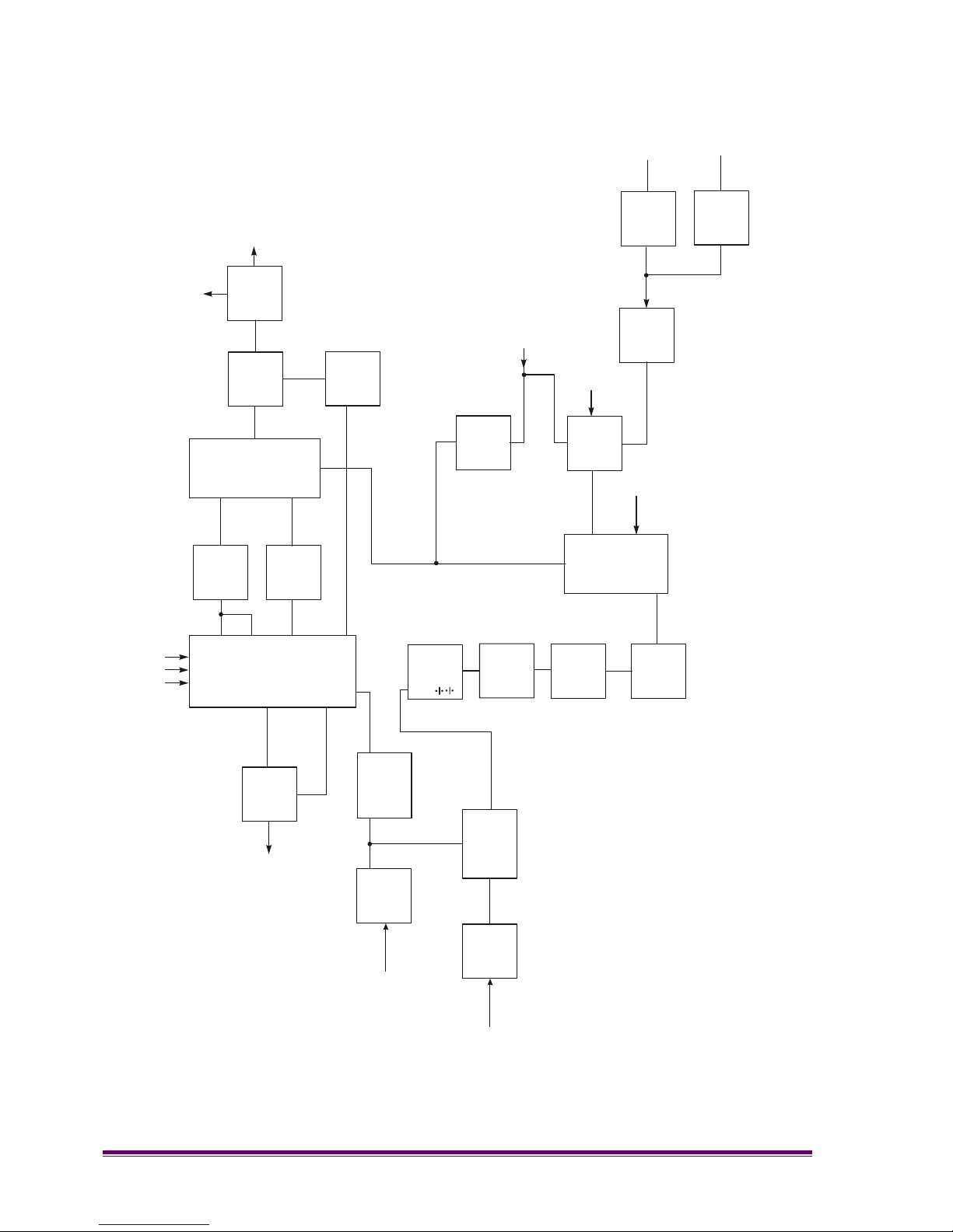
PAGE 44 TECHNICAL DESCRIPTION
Figure 3.7 - VHF/UHF Synthesiser, Block Diagram
L
o
o
p
F
i
l
t
e
r
C
7
3
4
/
7
1
9
/
7
2
2
9
0
M
H
z
L
O
Q
4
0
2
S
y
n
t
h
e
s
i
s
e
r
U
7
0
1
L
O
2
T
o
I
Q
D
e
m
o
d
u
l
a
t
o
r
U
4
0
1
A
U
X
L
O
2
A
U
X
C
P
C
P
P
C
P
P
F
S
Y
N
T
H
D
O
U
T
V
C
A
P
B
I
A
S
V
C
O
N
e
g
B
i
a
s
S
u
p
p
l
y
Q
7
0
0
/
7
0
1
/
7
0
2
/
7
0
3
R
x
/
T
x
V
C
O
Q
6
0
0
/
6
0
2
V
C
O
B
u
f
f
e
r
Q
6
0
4
/
6
0
5
T
x
/
R
x
S
w
i
t
c
h
D
6
0
1
/
6
1
1
T
o
R
x
M
i
x
e
r
L
O
1
R
x
T
o
T
x
B
u
f
f
e
r
S
y
n
t
h
B
u
f
f
e
r
Q
6
0
7
F
r
o
m
F
P
G
A
T
x
M
O
D
S
w
i
t
c
h
U
1
0
3
A
R
x
/
T
x
A
F
S
w
i
t
c
h
U
1
0
3
B
M
i
c
A
m
p
Q
8
1
2
I
A
F
C
I
N
M
O
D
1
O
N
T
x
M
O
D
1
A
D
C
/
D
A
C
C
O
D
E
C
U
8
0
0
Q
R
e
f
O
S
C
U
7
0
0
A
F
C
A
m
p
U
8
0
2
A
A
F
C
9
0
0
0
_
1
4
F
r
o
m
F
P
GA/DS
P
D
i
v
i
d
e
r
U
7
1
0
3
6
(
U
H
F
)
7
2
(
V
H
F
)
B
u
f
f
e
r
Q
7
1
0
F
X
T
A
L
P
h
a
s
e
M
o
d
u
l
a
t
o
r
Q
7
1
4
/
7
1
5
/
7
1
6
R
a
m
p
G
e
n
Q
7
1
1
/
7
1
2
/
7
1
3
B
u
f
f
e
r
U
7
1
1
/
B
L
o
w
P
a
s
s
F
i
l
t
e
r
U
7
1
1
/
A
T
x
M
o
d
1
T
u
n
e
B
a
l
G
a
t
e
U
1
0
7
G
a
t
e
U
1
0
8
A
u
d
i
n
1
M
i
c
A
u
d
i
o
O
p
t
i
o
n
A
u
d
i
o
a
n
d
D
a
t
a
I
n
p
u
t
Page 45
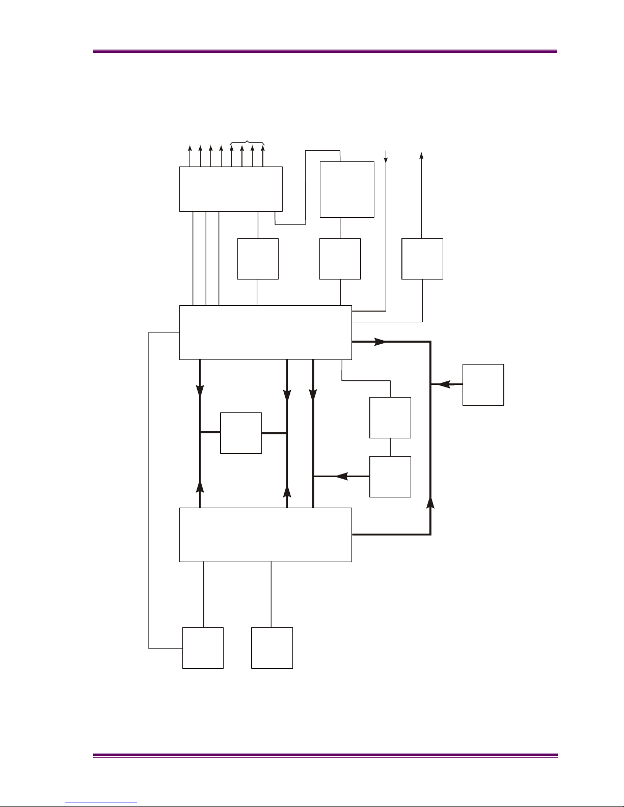
XFIN-BLADE-SM
TECHNICAL DESCRIPTION PAGE 45
4.3.5 RF Sub-Assembly Internal Control Logic
Figure 3.8 - VHF/UHF Control Block Diagram
9
0
0
0
_
1
5
C
l
o
c
k
Q
1
0
0
R
e
s
e
t
U
1
0
1
D
S
P
U
1
0
2
F
P
G
A
U
1
0
6
F
l
a
s
h
M
e
m
o
r
y
U
1
0
4
S
y
n
t
h
e
s
i
s
e
r
U
7
0
1
L
o
o
p
V
o
l
t
s
R
a
m
p
G
e
n
U
1
0
5
C
A
D
C
/
D
A
C
C
O
D
E
C
U
8
0
0
M
u
l
t
i
p
l
e
x
e
r
U
9
0
2
T
x
P
o
w
e
r
C
o
n
t
r
o
l
B
u
f
f
e
r
U
8
0
2
B
M
O
V
E
X
L
o
o
p
V
o
l
t
s
M
U
X
E
N
M
U
X
A
O
M
U
X
A
1
A
U
X
C
T
L
F
E
T
u
n
e
F
r
o
n
t
E
n
d
T
u
n
e
B
u
f
f
e
r
U
9
0
1
A
F
r
o
n
t
E
n
d
V
a
r
i
c
a
p
N
e
g
V
o
l
t
s
L
e
v
e
l
T
r
a
n
s
l
a
t
o
r
Q
9
0
0
/
9
0
1
/
9
0
2
/
9
0
9
R
x
D
a
t
a
T
x
D
a
t
a
S
e
r
i
a
l
P
o
r
t
S
e
r
i
a
l
P
o
r
t
A
G
C
T
x
P
o
w
e
r
S
e
t
A
T
o
n
e
A
D
C
R
e
f
T
u
n
e
1
-
4
T
x
D
a
t
a
B
u
f
f
e
r
Q
1
Page 46

PAGE 46 TECHNICAL DESCRIPTION
4.3.5.1 DSP and FPGA
The Blade RF sub-assemblies operate under the control of a DSP (U102) and FPGA
(U106) combination which together with a number of other dedicated devices perform all
the operational and processing functions required by the radio. The FPGA is configured by
the DSP under software control to provide the following functions:
• Channel set-up for operating frequency
• Modulation processing and filtering
• De-modulation processing and filtering
• TX power output reference
• Receiver front-end tuning
• Serial communications with control board
• Modem functionality for data modulation
• Embedded signalling / CTCSS generation and decoding
• CO control
• Receiver muting control
• TX / RX switching
• PLL detect
4.3.5.2 DSP Clock Oscillator
The DSP is clocked by a 15.360MHz oscillator that consists of crystal X100 and an
internal DSP oscillator. Q100 forms a crystal switching circuit with C117 which when
activated by a command from the FPGA steers the oscillator away from potential
interfering frequencies.
4.3.6 RF Sub-Assembly Internal Memory
Memory consists of the internal DSP memory and an external 4MB non-volatile Flash
Memory U104. When power is off, program and data is retained in Flash Memory. At
power-on, a boot program downloads the DSP’s program from Flash Memory to its
internal RAM for faster program execution and access to data.
4.3.6.1 Multiplexer
U902 contains 2 separate 4-channel multiplexers providing a total of 8 independently
controlled analogue switches. Under software control, the multiplexers produce tuning
voltages from supplied data for the receiver front-end (TUNE 1 to 4), TX power setting (TX
PWR SET), receiver AGC (AGC-1), alert tone (A TONE) and FPGA ramp generator (ADC
REF).
Buffer U802B is fed with a composite digital tuning signal (AUX CTL) from the DSP/FPGA
containing the data for AGC, A TONE, ADC REF and TX PWR SET settings. The level is
dependent on channel frequency and tuning and varies between 0.1 to 3.0V. This signal is
applied to one group of 4 analogue switches in U902 via a common input connected to pin
13. The second group of 4 switches is fed with the receiver front-end tuning signal FE
TUNE (to provide outputs for TUNE 1 to 4) via the second common input at pin 3 as
described in the receiver front-end section.
Page 47

XFIN-BLADE-SM
TECHNICAL DESCRIPTION PAGE 47
The 2 groups of analogue switches are independently controlled by FPGA binary signals
MUX A0 and A1 and enable line MUXEN to output the required tuning voltages as a series
of pulses. These pulses are converted to steady state voltages by integration capacitors
C904 to 911 and C921 to 925.
4.3.7 RF Sub-Assembly Internal Power Supplies
4.3.7.1 Power On Function
This set of functionality is designed for normal use in a vehicle environment; hence much
of it is unused in this product.
The unregulated 13.8V DC input is routed directly to high current devices and is also
switched via FET Q350. The output from Q350 feeds three, low drop out series regulators
and associated switched and auxiliary supplies that along with a negative voltage
generator provide all the switched power requirements of the transceiver.
Q315/316/317 and U313 form a power on/off latch circuit that is activated by a pulse from
the control unit or microphone/handset via PWR ON or PWR OFF and controls the FET
power switch Q350. A PWR OFF operation requires the button to be held down for more
than 2 seconds. This is then sensed by the FPGA via the PWR SENSE line that turns the
radio off by placing a positive pulse on the PWR OFF line thereby resetting U313B.
4.3.7.2 Power Lines
The following is a list of the internal RF Sub-Assembly’s power supplies and some of the
devices and circuits they supply.
+8V Regulator U310
Regulated +8.0V supply (8V0 and +8V)
• TX buffer Q612
• VCOs and VCO buffers via active filter Q615
• RX second local oscillator via Q403
Regulated +8.0V switched supply (RX PSU)
• RX front-end
• IF Amplifier
• Various switching functions
+5V Regulator U311
Regulated +5.0V supply (5V0 and +5V)
• RX front-end varactor positive bias
• Synth. buffer Q607
• VCO varactor negative supply Q700 to Q703
• TCXO U700
• RX audio amplifiers U803A/B
• RX mute switch Q810/813
• Multiplexer U902
• FE TUNE level translator and buffer U901A, Q900/901
Regulated +5.0V switched supply (TX PSU and TX PSU+)
• TX power control U3
Page 48

PAGE 48 TECHNICAL DESCRIPTION
• TX buffer Q606
• Microphone amplifier Q812
• Various switching functions
+3.3V Regulator U312
Regulated +3.3V supply (3N3)
• Digital supply for CODEC U800
• DSP U102
• FPGA U106
Regulated +3.3V supply (3Q3)
• I Q demodulator U401
Regulated +3.3V supply (3C3)
• Analogue supply for CODEC U800
Regulated +3.3V supply (3P3)
• PLL U701
• TCXO divider U702
Unregulated 13.8V (13V8 UNSW)
• TX PA module U2
• TX PA power control circuit Q3
• Active filter Q14/17/18/19
• Antenna changeover switch Q4/8/11
• RX mute switch Q811
• RX speaker amplifier U5
Negative Power Supply U300B/C
Provides -17.0V output (-17V0)
• Negative rail for VCO Varicap Negative Supply Q700, 701, 702 and Q703
-12.0V Output (-12V0)
• Negative rail for FE TUNE level translator Q900, 901, 902, 903 and
multiplexer U902
Page 49

XFIN-BLADE-SM
TECHNICAL DESCRIPTION PAGE 49
4.4 ANTENNA REQUIREMENTS
The antenna connections on the Blade are provided with 50Ω female N-type sockets.
These should be tested, by use of a suitable test set, e.g. Anritsu/Wiltron S331A, for good
VSWR (1.5:1 or better) at the Tx and Rx frequencies prior to use.
Mating connectors should be galvanically compatible with nickel outer and gold centre pin
to minimise passive intermodulation.
A minimum of 85dB transmit-receive isolation should be provided by the antenna system
and associated filters.
4.5 POWER SUPPLIES
For type approval reasons, this product should not be operated with un-approved supplies.
The switch mode supplies used in the wall mount and rack mount ancillaries are able to
accept main AC in the range of 100 to 240 V, 50 or 60Hz. The output from the switched
mode power supply to the Blade is +13.6VDC.
Pin 3 on the D-type Power Connector provides protective earthing on the equipment. This
should be connected using heavy duty Green/Yellow earthing wire, capacity greater than
mains feed to equipment, as few bends as possible and an appropriate eyelet tag.
Mains protective Earth should be checked for low impedance (<0.3Ω).
The equipment must be installed so that the IEC connector for the Wall or Rack Mount can
be easily removed and/or the power socket should be readily accessible.
All mains wiring must comply with local wiring regulations.
4.6 CONFIGURATION
Configuration is provided via file download. This is performed via the XBMT Programmer
using a PC connected to the Xfin Control card via its Ethernet port. Files are then stored in
the product in non-volatile memory.
Editing of parameters on a live base station is also possible with a connected PC.
4.7 ADJUSTMENT AND ALIGNMENT
The two RF modules within this product are based upon the RF card of an SRM9000
mobile. The set up and alignment procedures for SRM9000 should be followed. In the
event of a level-3 repair being required, refer to the SRM9000 Service Manual (TSD-
SRM9000-SM) [1].
There are no user adjustments to be made in normal use.
Page 50

Page 51

5 MAINTENANCE
Although no Routine Maintenance is required on the Blade, it is generally good practice to
clean the inside of the equipment on each occasion that it is necessary to open it.
Dust and or light debris may accumulate in the following areas:
• Fans
• Heatsinks
• Vents
Use a fine bristle brush to remove all dust/debris from these areas, taking care not to
damage the equipment.
5.1 TORQUE SETTINGS
The torque range to be used on tightening Torx screws and self-tapping screws on the
Blade and SRM sub-assemblies is 8-10Lb/in (0.90-1.13 Nm).
For all other small screws (Phillips/pozi head) use a maximum of 8 Lb/in (0.90Nm).
5.2 DISASSEMBLY
When disassembling any part of the Blade take care to note where parts belong.
5.2.1 To Remove the Blade from a Rack
When also fitted with associated PSUTRAY and shelf supports:
1. Switch off at mains.
2. Undo the screws holding the front panel of the PSUTRAY.
3. Disconnect and remove the PSUTRAY.
4. Undo the four screws securing the Blade Ears to the rack.
5. If the Blade is to be removed entirely, then disconnect all cables from the rear of the
equipment.
6. The Blade can now be lifted away from the shelf supports.
Page 52
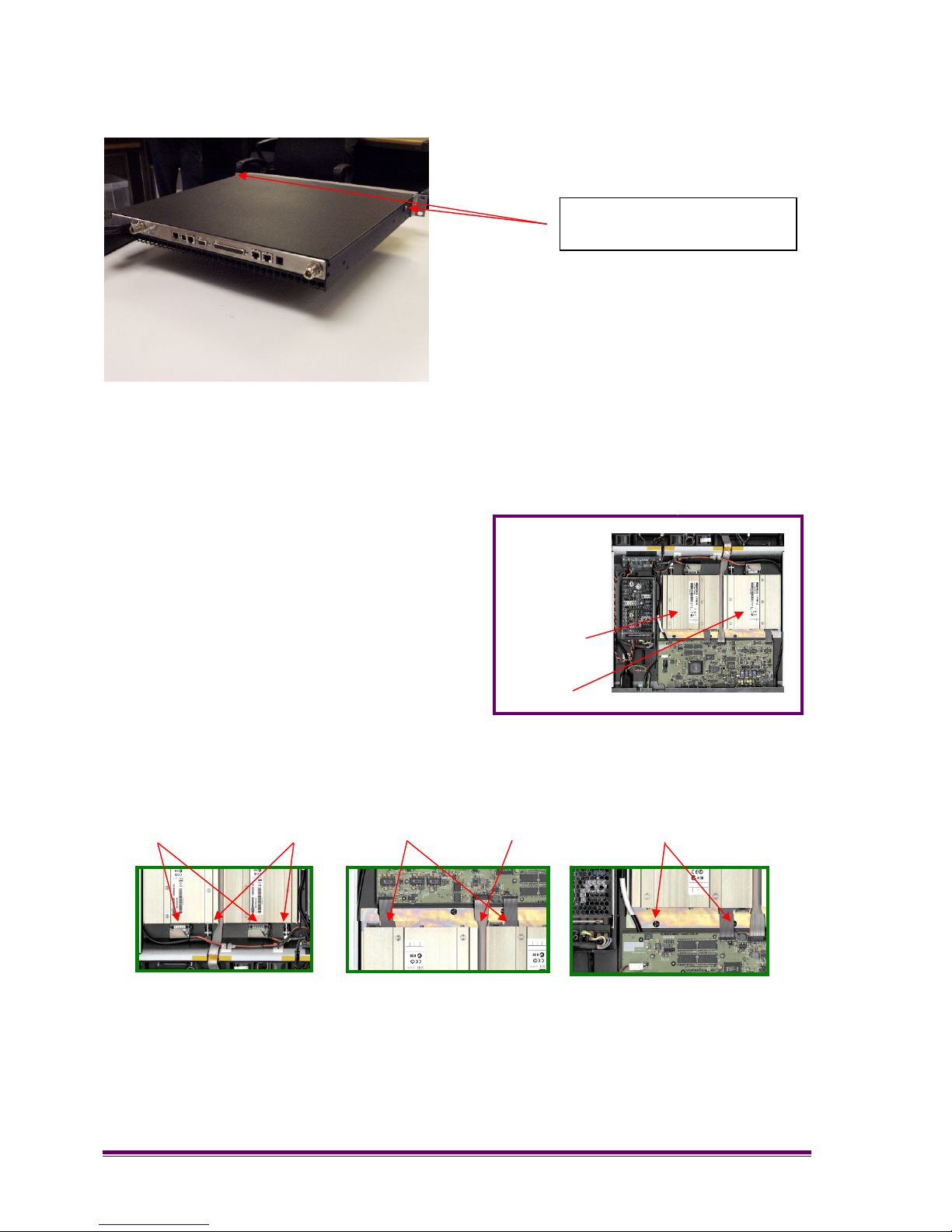
PAGE 52 MAINTENANCE
5.2.2 To Open the Blade
1. Remove the 2 x M3 Pan Head screws
one each side of the lid.
2. Lift and pull the front edge of the lid to
remove the lid.
5.2.3 To Remove a Tx or Rx Assembly
1. Disconnect the BNC connector.
2. Disconnect the DB15 power connector.
3. Disconnect the appropriate miniature 26-
way and the long ribbon cables (when
refitting, take care to align centrally).
4. Undo the two quarter-turn Dzus fasteners.
5. Lift the rear of the sub-assembly then
slide backwards until the Heatsink clears
the front lip of the recess (take care not to
damage any of the components on the
control board).
Receiver
Transmitter
BNC Connectors DB15 Connectors
Miniature Ribbon
Cables
Dzus Fasteners
Long Ribbon
Cable
Qty 2 Fixing Screws M3
Page 53
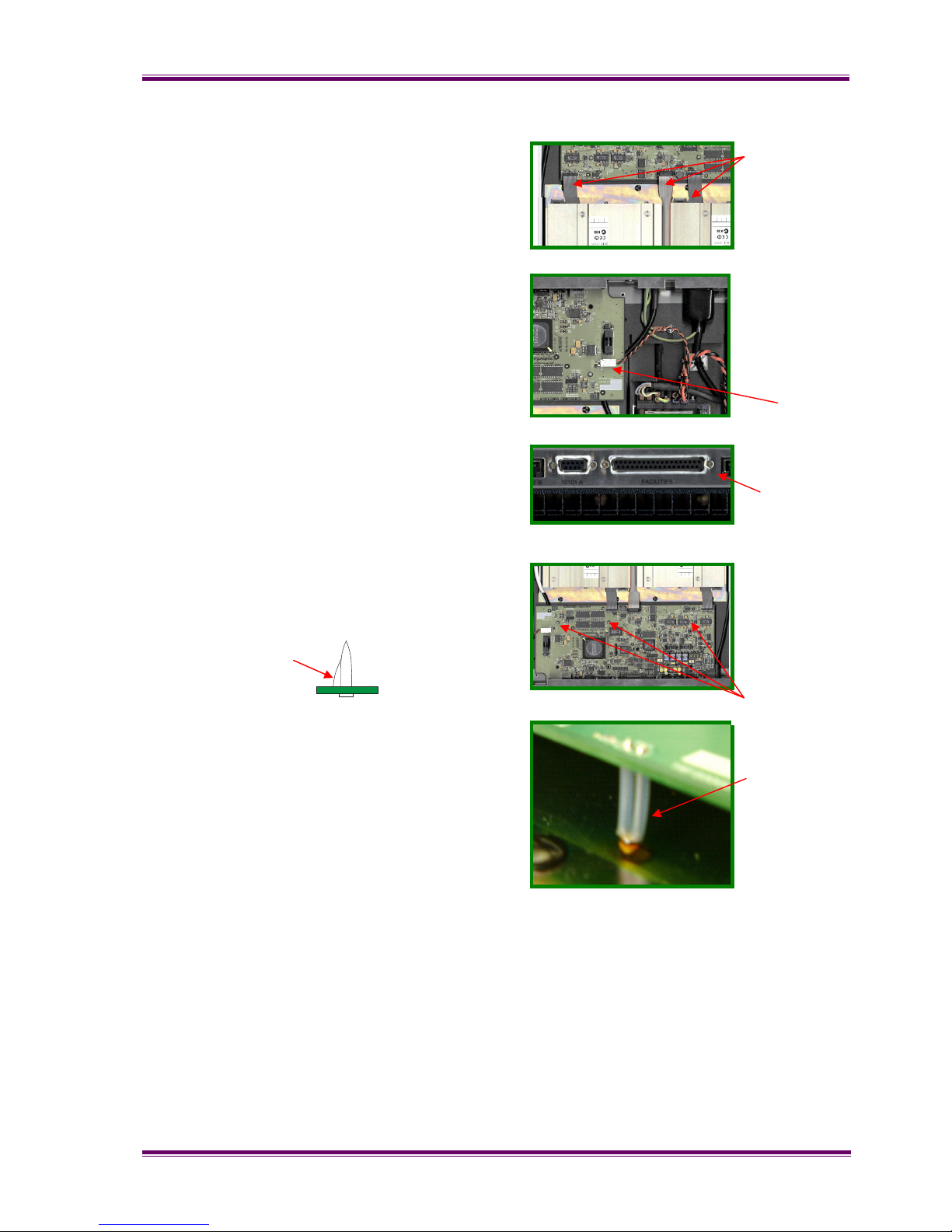
XFIN-BLADE-SM
MAINTENANCE PAGE 53
Ribbon Cables
5.2.4 To Remove the Control Board
1. Remove the top cover as detailed in
Section 4.2.3.
2. Disconnect the three ribbon cables from
the board.
3. Disconnect the Power Connector.
4. Remove the four socket fasteners from
the 9-way and 37-way connectors on the
rear panel.
5. Release the three plastic locking pegs.
6. Carefully lift out the board taking care not
to damage the Thermistor assembly
underneath the board. Ensure that the
Thermistor assembly is protected from
damage when the Control Board is out of
the Base Station chassis.
5.2.5 To Remove the Front Assembly
1. Remove the four, Front Panel securing screws – two per each side of the Front Panel
2. Carefully ease the front panel assembly away from the MMI assembly. Taking care to
prevent damage to the control knob.
3. Carefully separate the cables (power, fans, loudspeaker, control card) taking care not
to damage or unduly tension them.
Power
Connector
Socket
Fasteners
Thermistor
Press in to release
Plastic
Locking Pegs
Page 54

PAGE 54 MAINTENANCE
5.2.6 To Remove the MMI Board
1. Remove the front assembly as described in Section 5.2.5.
2. Remove the six securing screws from the chassis brackets.
3. Detach all of the cables (power, fans, loudspeaker, control card).
4. The MMI Board may now be removed.
5. To Remove the Loudspeaker, remove the front assembly and MMI board as
described above. Remove the four M3 nuts securing the Loudspeaker to the fan
bulkhead.
5.2.7 To Remove a Fan
1. Remove the Front assembly as described in Section 5.2.5 and the MMI board as
described in Section 5.2.6.
2. Remove the two fixing screws securing the appropriate Fan to the fan bulkhead.
3. Remove the Fan from the fan bulkhead.
5.3 RE-ASSEMBLY
In general, the re-assembly procedure is the reverse of disassembly procedure. If there
are any differences or there are any special areas of concern, they are described in this
section.
5.3.1 To Fit an MMI Board
1. Fit the new MMI Board to the three support brackets using six M3 mm Pan-Head
Screws.
2. Offer the front panel into position ensuring the top edge of the front panel clears the
control knob. Ensure that the LCD Display and the control knob are correctly centred.
3. Reverse the procedure described in Section 5.2.6.
5.3.2 To Fit the Front Assembly
1. Reverse the procedure described in Section 5.2.6 taking note of the following:
Notes: 1. Care must be taken to prevent damage to the cables and connectors when re-
locating them through the access slot in the fan bulkhead and reconnecting
them to the MMI board.
2. Care must be taken to prevent trapping the cables when fitting the front cover
back together with the fan bulkhead.
5.3.3 To Fit the Control Board
1. Reverse the procedure described in Section 4.2.5.
Note: When positioning the Control Board, care must be taken to ensure that the
Thermistor is located correctly in the hole in the base plate.
Page 55
XFIN-BLADE-SM
PRODUCT VARIANTS AND ACCESSORIES PAGE 55
6 PRODUCT VARIANTS AND ACCESSORIES
6.1 VARIANTS
Blade - Full-Duplex
Intelligent Base Station
25W Ext. PSU 25W Int. PSU 100W Version
66 - 88 MHz E0 Band XFINBLADE-E0 XFINBLADEI-E0 XFINPWRBLADE-E0
136 - 174 MHz AC Band XFINBLADE-AC XFINBLADEI-AC XFINPWRBLADE-AC
174 - 208 MHz K1 Band XFINBLADE-K1 XFINBLADEI-K1 XFINPWRBLADE-K1
208 - 245 MHz KM Band XFINBLADE-KM XFINBLADEI-KM XFINPWRBLADE-KM
310 - 350 MHz R0 Band XFINBLADE-R0 XFINBLADEI-R0 XFINPWRBLADE-R0
335 - 375 MHz R1 Band XFINBLADE-R1 XFINBLADEI-R1 XFINPWRBLADE-R1
400 - 450 MHz TK Band XFINBLADE-TK XFINBLADEI-TK XFINPWRBLADE-TK
400 - 480 MHz TU Band XFINBLADE-TU XFINBLADEI-TU XFINPWRBLADE-TU
440 - 500 MHz UW Band XFINBLADE-UW XFINBLADEI-UW XFINPWRBLADE-UW
470 - 530 MHz WR Band XFINBLADE-WR XFINBLADEI-WR XFINPWRBLADE-WR
6.2 ACCESSORIES
The full range of accessories for the Blade is shown on the two Blade Accessories
Posters.
Accessories for MIC Connector
TSF Serial Programming Lead with adaptor (DB-
9)
TSFPROGLEAD
Wall Mount Installation Items
Wall Mount Unit with universal PSU (for single BS) TSF-WMPS
Mains Cord for Wall Mount unit (EU/UK/US - select country) TSF-ACCORD-EU
TSF-ACCORD-UK
TSF-ACCORD-US
Duplexer option for wall-mount use TSF-DUPxx (where xx =
freq band)
Page 56

PAGE 56 PRODUCT VARIANTS AND ACCESSORIES
Rack Mount Installation Items
Rack Mount Ears (1U)
TSF-EARS
Rack mount PSU tray (1 base station, 2U) 25 WATT TSF-PSUTRAY
Rack mount PSU tray (1 base station, 2U) 100 WATT TSF-2100PSUTRAY
Duplexer for PSUTRAY (specify frequencies – TSF only) TSF-DUPxx (where xx =
freq band)
Mains Cord for PSUTRAY (EU/UK/US - select country) TSF-ACCORD-EU
TSF-ACCORD-UK
TSF-ACCORD-US
6.2.1 TSF-ACCORD
A 2m long cable used to connect the AC Mains Supply to the Blade, using the Wallmount,
or a PSUtray in the Rackmount. Request the version relevant to the area of use:
• TSF-ACCORD-UK United Kingdom
• TSF-ACCORD-EU Rest of Europe
• TSF-ACCORD-US United States
6.2.2 Duplexers, Combiners, Cavities, RSA Units
Where a duplexer, combiner, cavity or Rx Antenna Amplifier must be re-ordered, an
enquiry should be made to a qualified Project Engineer, who can advise on specific
components.
Page 57

XFIN-BLADE-SM
PRODUCT VARIANTS AND ACCESSORIES PAGE 57
6.2.3 TSF-EARS
A pair of 1U Rack Mounting Ears with screws for the Blade Base Station.
These must be used in conjunction with a rack-support
6.2.4 TSF-PROG
The TSF Serial Programming Lead contains an RS232 level converter. Together with the
adaptor (DB-9) it can be used to connect the Blade, via the front panel RJ45 connector, to
a PC.
6.2.5 Blade Shelves
Where a re-ordering enquiry is made with regard to Blade shelving, a qualified Project
Engineer should be consulted to give advice.
Order code for a PSU tray for Blade systems involving 1-3 basestations:
PSU Trays for Blade Systems with 1-3 Basestations
Rack mount PSU tray (19” 1U for 1x 25W Blade) TSF-1PSU1U
Rack mount PSU tray (19” 1U for 2x 25W Blade) TSF-2PSU1U
Rack mount PSU tray (19” 1U for 3x 25W Blade) TSF-3PSU1U
6.2.6 TSF-1BS PSUTRAY
A 2U-rack tray with front panel is designed for use with a Blade in an enclosed 19” rack where duplexers
must be shelved alongside power supplies. The Blade plus the TSF-PSUTRAY occupies a total of 3U of
rack space.
The tray is supplied complete with a universal power supply (100-240VAC, 50/60Hz, IEC input) suitable for
a single Blade.
TSF-DUPLEXER may be fitted as an option.
An optional PSU may be used with the Power Blade configuration.
6.2.6.1 TSF-1BS PSUTRAY Specifications
• Dimensions: 480mm(W) x 400mm(D) x 90mm(H).
• Weight: 3.95kg.
• Mains Connector: IEC
• Power requirement: 150W
• Fuse Rating: 110V: T250V 4A HB
250V: T250V 2A HB.
• Blade Cable: Approx. 300mm
Page 58

PAGE 58 PRODUCT VARIANTS AND ACCESSORIES
Page 59

7 SPARES
7.1 SERVICE CONCEPT
The Blade series has been designed to provide a low cost trunked and non-trunked,
analogue, base station, using common core electronics, software and interfacing.
It is a requirement that once the customer has purchased equipment, Team Simoco can
follow this by providing ongoing, high level of customer support together with a competitive
and professional servicing activity.
There are three levels of service available:
Level Activity Recommended
Spares
Recommended Test
Equipment and tools
1 This is intended to achieve
rapid turn around by –
• Complete replacement
of transceiver or
ancillaries
• Replacement of subassemblies
• Reprogramming
• Checking/replacement
of fuses
Faulty units are to be
returned to a level-2
service facility with an
attached fault report.
This level of service should
not exceed 20 minutes.
SRM sub-assembly
(by band)
Control board
MMI board
Fan
Spare cable assys.
Replacement fuses
Multimeter
P.C. with Programmer
Engineering handset
Small flat-blade
screwdriver
Small cross-head
screwdriver
Large pozi-drive
screwdriver
2 Level 2 service includes
level 1 with the addition of
fault rectification by:
• Replacement of PCB,
mechanical component,
or cable assembly
Cosmetic repair
Listed in Level 2
Spares Schedule
Spare parts
available to order
from Central Spares
As above + service aids
and test equipment
3 Repair by PCB or
mechanical component
replacement, Cosmetic
repair.
Repair of PCB to
component level in CRU.
Listed in Level 2
Spares Schedule
Radio PCB
components only
available to CRU.
As above + service aids
and test equipment
Page 60
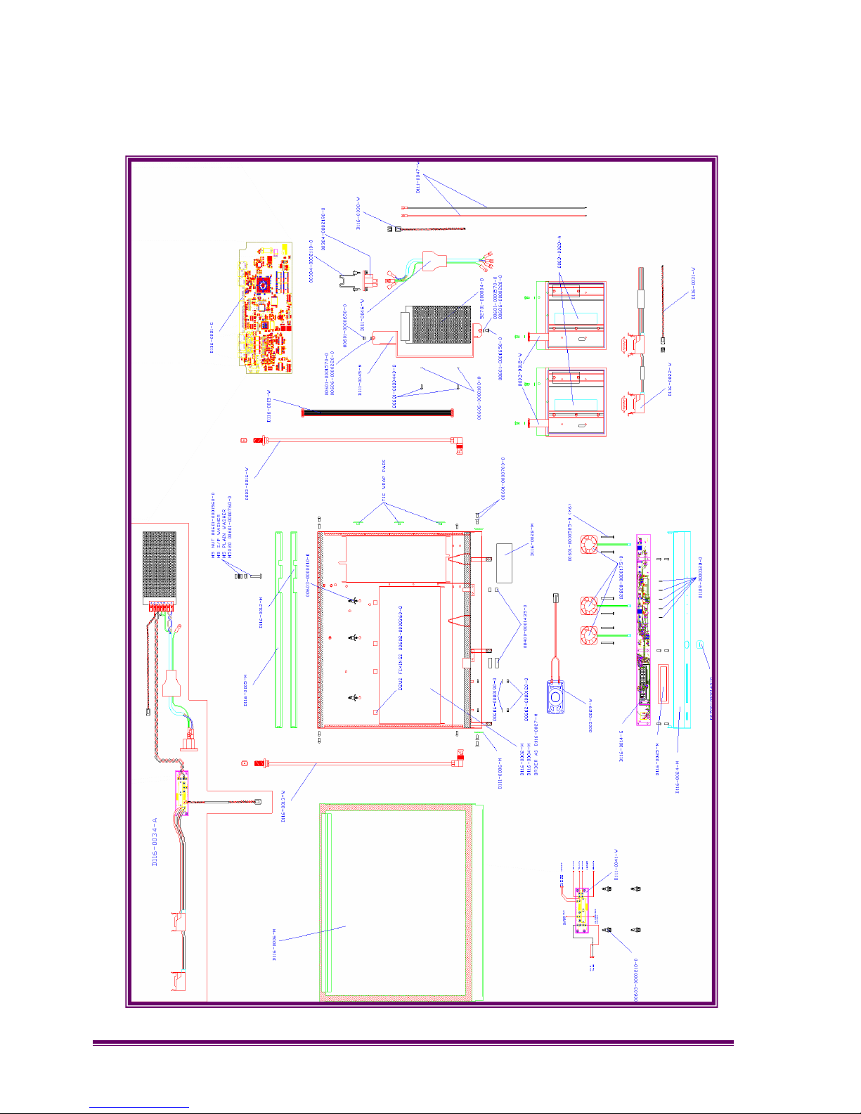
PAGE 60 SPARES
7.2 LEVEL-2 SPARES SCHEDULE
7.2.1 XFIN BLADE (INTERNAL PSU VERSION)
Figure 6.1 Exploded Diagram of the Xfin Blade
Page 61
XFIN-BLADE-SM
SPARES PAGE 61
7.2.2 Assembly Item List
Part Number Part Description Quantity
D116-0027-M-01 CASE BULKHEAD X/FIN 1
D116-0024-M-05 X-FIN FRONT PANEL (SOLID FRONT) 1
D116-0006-M-03 LID ASSY X/FIN 1
00601-0001630-0 M3X8 SCREW PAN HD POZI STL/S 2
00606-000540-0 M3 PLAIN WASHER STAINLESS/STL. 2
D116-0012-M-04 230V REAR PANEL 1
D116-0025-M-01 TSC 2000 WINDOW PROTECTION 1
D116-0028-M-02 INSULATION PAD TSF/XFIN 1
D111-0042-M-02 TSF2025I INT PSU BRKT (LAMBDA) 1
0003-0001-M-07 RACK MNTG EARS TSF2000 2
D111-0006-M-01 TSF WALL MOUNTING EAR 2
0003-0029-W-03 TSF LOUDSPEAKER ASSY 1
02800-0000175-0 FAN TYPE 412J/2H-T224-730Q 3
D111-0041-G-01 TSF2000 FUSE BOARD 1
02700-0000140-0 KNOB CONTROL SILVER 25MM 1
01109-0000120-0 LIGHT GUIDE 14mm ROUNDED 5
00304-0002190-0 CONNECTOR IEC FLANGED 1
00304-0002110-0 CONNECTOR CLIP RETAINING 1
D116-0013-W-02 RF CABLE RX TSC2000 1
D116-0022-W-01 X/FIN DC POWER LOOM INTERNAL 1
D116-0015-W-02 TSC2000 PA TO CTRL PCB CBL FRM 1
0003-0018-W-01 RIBBON CABLE RX/TX SRM 2
D116-0014-G-03 MMI ASSY - X/FIN 1
D116-0001-G-03 CONTROL BOARD ASSY - X/FIN 1
59800-0000034-0 FUSEHOLDER PCB 20X5MM 1
00806-0000130-0 FUSE COVER CLEAR 1
00804-0000002-0 FUSE 10A Q/BLOW GLASS 20MM 2
00804-0000180-0 2A 20MM QB GLASS 1
52701-0000040-0 PSU 12V 150W (TSF2025i) 1
00602-0000360-0 RECEPTACLE DZUS 334-200-190 4
00603-0000210-0 PCB SUPPORT - BLIND HOLE 4.8mm 4
3513 903 67181 LABEL T/A & UNIT SRM9000 3
00601-0001660-0 M3X8 PAN HD POZI-BLACK 4
00601-0000420-0 M3 X8 POZI P/HD BZP 6
00601-0000585-0 M3 X 30 POZI P/HEAD 6
00601-0000700-0 M4 X10 CSNK POZI 4
00601-0000760-0 M5 X20 POZI P/HD BZP 1
Page 62

PAGE 62 SPARES
00602-0000120-0 M3 NUT BZP 8
00601-0001560-0 NUT M5 HEX STEEL ZINC PLATE 3
00606-0000220-0 M4 PLAIN WASHER BZP 2
00601-0001570-0 S/P WASHER STEEL ZINC/P M4 2
00601-0000440-0 M3 X10 POZI P/HD BZP 2
00606-0000180-0 M3 PLAIN WASHER BZP 2
00601-0000650-0 M4 X 6 P/HD POZI 2
D111-0046-W-03 IEC CONN TO LAMBDA PSU CBL 1
00606-0000190-0 M3 S/P WASHER BZP 4
0003-0016-W-01 TSF2000 RX TX CABLEFORM 1
00601-0001570-0 S/P WASHER STEEL ZINC/P M4 2
00601-0001580-0 WASHER PLAIN M5 ZINC PLATE 2
D116-0031-W-01 XFIN MMI TO FUSE PCB CBL FORM 1
01202-0000150-0 XFIN PACKING BOX 1
01202-0000160-0 XFIN PACKING BAG 1
01202-0000170-0 XFIN ETHER FOAM PACKING 1
PA-ACCORD-UK CORD AC POWER UK 1
D116-0030-W-01 XFIN CTRL PCB TO PSU CBL FRM 1
02313-0000010-0 ENCODER 15mm KNURLED SHAFT 1
01108-0000010-0 DISPLAY LCD WHITE/BLUE 1
7.3 WARRANTY
Unless superseded by specific contractual/supply agreements, the normal statutory 24 month warranty will apply to all base stations and ancillaries.
7.3.1 Service Within and Out Of Warranty
Please contact our Central Repair facility regarding support of either type.
Tel: +44 (0)1332 375620
In some countries a local Simoco agent may be responsible for providing this service.
7.3.2 Ancillary Items
Please contact our Central Repair facility regarding service, for replacement of these
parts.
Tel: +44 (0)1332 375620
7.3.3 Unpacking Equipment
Any damaged or missing parts must be notified to Team Simoco or their agent in writing
within 10 days of receipt.
Page 63

XFIN-BLADE-SM
SPARES PAGE 63
7.4 SOFTWARE POLICY
Software provided by Team Simoco shall remain the Company's property, or that of its
licensors and the customer recognises the confidential nature of the rights owned by the
Company.
The customer is granted a personal, non-exclusive, non-transferable limited right of use of
such software in machine-readable form in direct connection with the equipment for which
it was supplied only.
In certain circumstances the customer may be required to enter into a separate licence
agreement and pay a licence fee, which will be negotiated at the time of the contract.
The customer undertakes not to disclose any part of the software to third parties without
the Company's written consent, nor to copy or modify any software. The Company may, at
its discretion, carry out minor modifications to software. Major modifications may be
undertaken under a separate agreement, and will be charged separately.
All software is covered by a warranty of 3 months from delivery, and within this warranty
period the Company will correct errors or defects, or at its option, arrange free-of-charge
replacement against return of defective material.
Other than in the clause above, the Company makes no representations or warranties,
expressed or implied such, by way of example, but not of limitation regarding
merchantable quality or fitness for any particular purpose, or that the software is error free,
the Company does not accept liability with respect to any claims for loss of profits or of
contracts, or of any other loss of any kind whatsoever on account of use of software and
copies thereof.
Page 64

PAGE 64 SPARES
Page 65

XFIN-BLADE-SM
LCD MENU OPERATION PAGE 65
8 LCD MENU OPERATION
8.1 DEFAULT DISPLAY
The LCD Display is a back-lit alphanumeric 2-line visual output which shows status, menu
options and call activity.
Immediately following power-up, the LCD indicates its progress through the boot-up
procedure. A typical sequence is:
BLADE Xfin Loading…
Init
Available
Additional status changes include adoption of Control status, ‘*’ marker indicating
assumption of site master status and the ‘#’ marker which indicates assumption of system
master status (in a multi-site configuration).
8.2 MENU STRUCTURE
The Xfin Blade menu is manipulated via the control knob. Rotating the knob while in
default state will alter the loudspeaker volume setting.
Pressing the knob once from the default display opens the main menu, with the current
option displayed on the screen. Rotating the control knob cycles through the available
options, which are:
1. Alarms
2. Set IP Address
3. Set Position in Site
4. Set Site ID
5. Set System ID
6. Enable Screen Saver
7. Test Menu
8. Exit
Where a menu selection gives the option of altering parameters (e.g. entering a series of
digits), this may be carried out by:
• moving the underline cursor to the variable in question by rotating the knob
• pressing the button to select the digit
• rotating the knob to alter the value
• pressing the knob to set the digit
Page 66

PAGE 66 LCD MENU OPERATION
• moving the cursor to the tick mark at the side of the screen when all
variables are altered and pressing to confirm (an ‘x’ on the other side of the
screen can be selected to cancel the alteration).
Where a variable can only be increased or decreased, no cursor, tick or ‘x’ symbols are
present.
8.2.1 Alarms Menu
If the ‘Alarm’ LED is lit (red LED on the far right hand side of the Blade front-panel), the
Alarms menu will display the details of each alarm – for example “Tx Fan Too Slow”, “No
DSP”, “No Rx Module” etc. Each alarm message is displayed by rotating the control knob.
8.2.2 Set IP Address
Accessing this menu displays the current IP address as four 3-digit sections. This address
may be altered from this section.
8.2.3 Set Position in Site
Accessing this menu displays the current position in site as a 2-digit decimal number. This
number may be altered from this section.
8.2.4 Set Site ID
Accessing this menu displays the current site ID as a 2-digit decimal number. This number
may be altered from this section.
8.2.5 Set System ID
Accessing this menu displays the current system ID as a 2-digit decimal number. This
number may be altered from this section.
8.2.6 Enable Screen Saver
This section allows the user to enable the screen saver. The screen saver activates after
the LCD menu has not been accessed for a set period.
8.2.7 Test Menu
This menu is for engineering use only and should only be access by qualified personnel. It
can be used to assist with the configuration of audio levels and the testing of
communication paths.
8.2.8 Exit
Select this option to exit the menu and revert to the display of current status..
Page 67

XFIN-BLADE-SM
PROGRAMMER GUIDE PAGE 67
9 PROGRAMMER GUIDE
9.1 GETTING STARTED
Ensure that the PC is connected to the Xfin Blade Management Terminal via a CAT 5
Ethernet cable or a RS232 Serial cable. This provides the communications link between
the Xfin Blade Management Terminal and the Xfin Blade.
9.1.1 Main Screen
The main menu by default displays clickable buttons of several configurable areas. Some
areas will be hidden depending on whether the Xfin Blade Management Terminal is in
Single Site or Multi Site. The areas are:
• Switch
• Site Configuration
• Xfin Blades
• Channels
• Channel Lists
• PABX/PSTN
• Operating Parameters
• Fleets
• Subscribers
• Access Levels
• Diversions
• White List
• Timers
• Time Schedule
• External Alarms
• Queue Depths
• VOX
9.2 DATABASE
The Xfin Blade Management Terminal requires a database to be created to store raw
data. This data can then used to configure an Xfin Blade. When configuring the Xfin Blade
data is taken from the database and sent to the Xfin Blade. Data that the Xfin Blade
Management Terminal receives from the Xfin Blade is also stored within the database.
9.2.1 Creating a New Database
Located across the top of the Main Menu form there is a menu bar. To create the new
database click on Database tab, then select New from the drop down. A window will
Page 68

PAGE 68 PROGRAMMER GUIDE
appear allowing a new database to be created in a location of choice. Use the save in drop
down box to navigate to the area where the database is to be stored. Give the database a
name using the File Name box and then click on save. Clicking on cancel instead would
bring back the main menu form.
9.2.2 Opening a Database
Multiple databases can be created however the Xfin Blade Management Terminal will only
use one database at a time. Xfin Blade Management Terminal offers the ability to switch
between the databases by selecting Database from the menu bar at the top of the form,
and clicking Open in the drop down. Using the Look in drop down box navigate the
database to be opened. Select the database by clicking on the database to highlight it.
Now select the button Open which will load in that database. Clicking cancel instead will
bring back the main menu.
9.3 COMMUNICATIONS SETTINGS
To connect to the Xfin Blade the communications settings will first need to be altered. This
is located in the menu bar running across the top of the form, under Communications. On
this form there are options for Ethernet and Serial.
9.3.1 Connection Type
There are two options Ethernet via CAT 5 cable, or Serial via RS232. Select the type of
connection by left clicking on one of the radio buttons in the Ethernet Communications
box.
9.3.2 Serial Communications
The Serial Communications needs to be configured when Serial is selected in the
Connection Type box. There are five setting in the Serial Communications:
• Com Port – This is the serial communication port being used to connect to the Xfin
Blade. To select a Com Port click on the arrow in the box to the right of Com Port
and select a Com Port from the drop down list.
• Baud Rate – This is the speed at which the data is passed through the serial
connection. To Select a Baud Rate click on the arrow in the box to the right of Baud
Rate and select a Baud Rate from the drop down list.
• Parity – This is a type of error detection using bit checking. To select a Parity click
on the arrow in the box to the right of Parity and select a Parity from the drop down
list.
• Stop Bits – This is the bit that signals the end of a transmission on the serial line.
To select a Stop Bit click on the arrow in the box to the right of Stop Bit and select a
Stop Bit from the drop down list.
• Flow Control – This is used to regulate the rate at which information is transferred
from one device to another. To select a Flow Rate click on the arrow in the box to
the right of Flow Rate and select a Flow Rate from the drop down list.
Now that the Serial Communications setting have been configured click on Save & Exit to
menu to the main menu. Alternatively click on refresh to set the setting back to what they
were when the Communications Settings form was first opened.
Page 69

XFIN-BLADE-SM
PROGRAMMER GUIDE PAGE 69
9.3.3 Ethernet Communications
The Ethernet Communications options needs to be configured when Ethernet is selected
in the Connection Type box. There are four settings in the Ethernet Communications:
• Connect to Site Master/Connect to System Master – This option allows you to
choose whether to connect to the Site master or if you want to connect to the
System master.
• Site ID – This is the ID of the site that you want to connect to. The Site ID is set
from a Xfin Blades front panel.
• System ID – This is the ID of the system that you want to connect to. The System
ID is set from a Xfin Blades front panel.
• UDP Listening Port – This is the port that the Xfin Blade Management Terminal
listens for a connection on. To set this port, click on the box to the right of UDP
Listening Port and enter a port number. The default value for this port is 4950.
Now that the Ethernet Communications setting have been configured click on Save & Exit
to menu to the main menu. Alternatively click on refresh to set the setting back to what
they were when the Communications Settings form was first opened.
9.3.4 Open Comms
To be able to send messages to the Xfin Blade, communications firstly has to be
established between the Xfin Blade Management Terminal and Xfin Blade. Ensure that the
Communication settings are correct.
From the main menu window select Communications from the menu bar that is located
across the top of the form. Left click on Open Comms from the drop down list. The Xfin
Blade Management Terminal will now attempt to connect to the Xfin Blade. If the Xfin
Blade Management Terminal was successful then Established will be displayed in the
button left hand corner of the main menu.
If the Xfin Blade Management Terminal does not go in to Established then make sure that
the Communication Settings are correct and then retry connecting.
9.4 STATE
There are two states that the Xfin Blade Management Terminal can be in. The state will
determine how the Xfin Blade Management Terminal configures the Xfin Blade.
• Offline – When in offline mode any changes that are made to the data contained in
the Xfin Blade Management Terminal will not be sent to the Xfin Blade. To place the
Xfin Blade Management Terminal in to offline mode click on the small box in the
status bar of the main menu until it says offline.
• Live – When in live mode any changes that are made to the data contained in the
Xfin Blade Management Terminal will also be sent to the Xfin Blade. To place the
Xfin Blade Management Terminal in to Live mode make sure that the Live mode
click on the small box in the status bar of the main menu until it says live.
Page 70

PAGE 70 PROGRAMMER GUIDE
9.5 AREA CONFIGURATION
Choose an area from the main menu to configure by left clicking on one of the large
buttons, which are located in the middle on the main menu form.
The area form will now be shown with the configurable fields. The majority of the forms all
follow this same format and allow you to edit, add, delete, get, get configuration,
accept/send, send configuration and reset configuration. The mode effects differ if the Xfin
Blade Management Terminal is in Live or Offline state. When the Xfin Blade Management
Terminal is in Live mode the changes happen to the Xfin Blade Management Terminal and
the Xfin Blade. When the Xfin Blade Management Terminal is in Offline mode the changes
are only stored in the Xfin Blade Management Terminal.
9.5.1 Edit
To alter any of the fields shown on the form the form needs to be in edit mode. Once the
form is set to edit mode the boxes that were blanked out are now available for altering.
Edit mode will allow you to only alter an existing record.
To set the form in to edit mode left click on the Edit button located on the right hand side of
the screen. To get out of edit mode, click on accept or cancel. Accept will store the
changes, if any that have been made. Cancel will ignore any changes that have been
made and return back to its previous state.
9.5.2 Add
Add mode allows a new record to be added to the Xfin Blade Management Terminal. Left
click on the add button which is locate to the right of the form and an empty form will be
shown. Enter the required data in to all of the boxes.
To accept the record click on the accept button. To cancel the record, click on the cancel
button.
9.5.3 Delete
Delete will remove the current selected record that is being shown from the Xfin Blade
Management Terminal and the Xfin Blade depending on the state of the programmer. Left
click on the delete button located on the right hand side of the form to delete the record.
9.5.4 Accept/Send
Accept/Send will accept the record that is currently being show on the form. Accept/Send
will also send the record to the Xfin Blade as long as comms are established. Left click on
the Accept/Send button located on the right hand side of the form to Accept/Send a
record.
9.5.5 Get Record
As long as the Xfin Blade Management Terminal has established a connection to an Xfin
Blade Get Record will retrieve an update on the current selected record. To do a Get
Record left click on the Get Record button located on the right hand side of the form.
9.5.6 Send Configuration
As long as the Xfin Blade Management Terminal has established a connection to an Xfin
Blade Send Configuration will send every record for the current area to an Xfin Blade. To
Page 71

XFIN-BLADE-SM
PROGRAMMER GUIDE PAGE 71
Send Configuration left click on the Send Configuration button located on the right hand
side of the form.
9.5.7 Get Configuration
As long as the Xfin Blade Management Terminal has established a connection to an Xfin
Blade Get Configuration will retrieve every record that is store in the Xfin Blade for that
area. To Get Configuration left click on the Get Configuration button located on the right
hand side of the form.
9.5.8 Reset Configuration
Reset Configuration offers the user the choice to delete everything that is in the Xfin Blade
Management Terminal’s current database for that area or to delete everything in the
database for that area for the Xfin Blade and the Xfin Blade Management Terminal.
9.5.9 Navigation Buttons
One area can store multiple records and the form can only show one record at a time. The
navigation buttons located below the forms data boxes.
• The double arrow that points to the left displays the first record.
• The double arrow that points to the right displays the last record.
• The single arrow that points to the left displays the previous record.
• The single arrow that points to the right displays the next record.
Page 72

PAGE 72 PROGRAMMER GUIDE
Page 73

Team Simoco Ltd, Field House, Uttoxeter Old Road, Derby DE1 1NH
Tel: +44 (0) 1332 375500
FAX: +44 (0) 1332375501
www.teamsimoco.com
Page 74

A. GLOSSARY AND ABBREVIATIONS
TX Transmit
RX Receive
DSP Digital Signal Processor
USB Universal Serial Bus
MII Media-Independent Interface
JTAG Joint Test Action Group
EMI Electro-Magnetic Interference
GPIO General Purpose Input/Output
PCB Printed Circuit Board
PHY PHYsical layer interface
SDRAM Synchronous Dynamic Random Access Memory
UART Universal Asynchronous Receiver-Transmitter
MMI Man-Machine Interface
RTC Real Time Clock
PA Power Amplifier
CoDec Coder/Decoder
TSC Trunked Site Controller
RTS Request To Send (RS232 flow control signal)
CTS Clear To Send (RS232 flow control signal)
PSTN Public Switched Telephone Network
TBR Technical Basis for Regulation
LVD Low Voltage Directorate
NIC Network Interface Controller
LCD Liquid Crystal Display
SPORT Serial PORT of the digital signal processor
ROM Read Only Memory
NC Not Connected
E&M Ear and Mouth
DAA Data Access Arrangement
Page 75
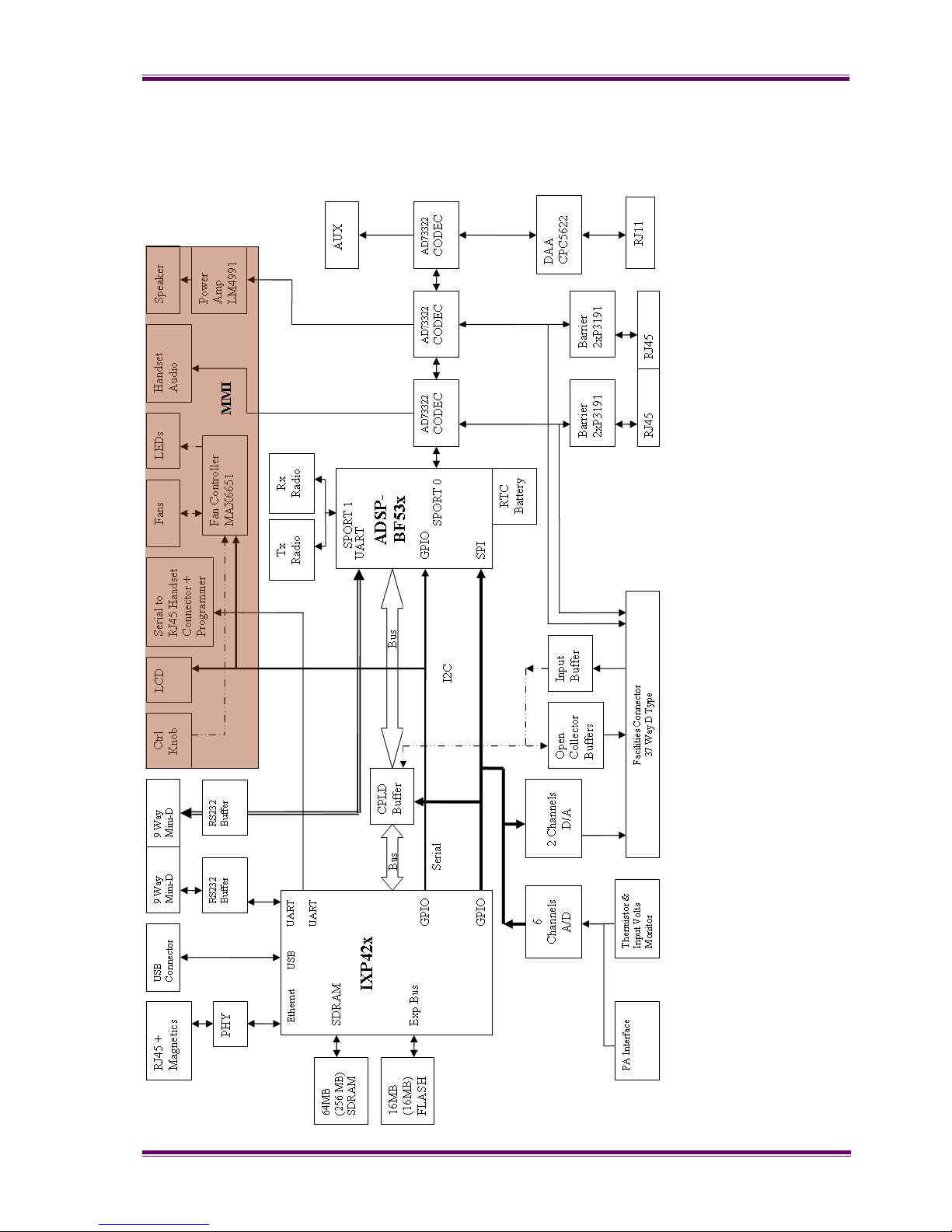
XFIN-BLADE-SM
CONTROL CARD BLOCK DIAGRAM PAGE 75
B. CONTROL CARD BLOCK DIAGRAM
Page 76

 Loading...