

Page 1
SIM8905A_User Manual_
V1.00
Page 2

Smart Machine Smart Decision
2
Compliance Information:
FCC Compliance Statement: This device complies with Part 15 of the FCC Rules . Operation is
subject to the following two conditions: 1. This device may not cause harmful interference, and 2.
This device must accept any interference received, including interference that may cause undesired
operation. This device must accept any interference received, including interference that may cause
undesired operation. Product that is a radio transmitter is labeled with FCC ID.
FCC Caution:
(1)Exposure to Radio Frequency Radiation. This equipment must be installed and operated in
accordance with provided instructions and the antenna(s) used for this transmitter must be installed
to provide a separation distance of at least 20 cm from all persons and must not be collocated or
operating in conjunction with any other antenna or transmitter. End-users and installers must be
provided with antenna installation instructions and transmitter operating conditions for satisfying RF
exposure compliance.
(2)Any changes or modifications not expressly approved by the grantee of this device could void the
user's authority to operate the equipment.
(3)This Transmitter must not be co-located or operating in conjunction with any other antenna or
transmitter.
(4)Changes or modifications to this unit not expressly approved by the party responsible for
compliance could void the user authority to operate the equipment.
(5) the modules FCC ID is not visible when installed in the host, if the host is marketed so that
end users do not have straight forward commonly used methods for access to remove the module so
that the FCC ID of the module is visible; then an additional permanent label referring to the enclosed
module: Contains Transmitter Module FCC ID: 2AJYU-8PSA301 or Contains FCC ID: 2AJYU-8PSA301.
The following statement must be included with all versions of this document supplied to an
OEM or integrator, but should not be distributed to the end user.
This device is intended for OEM integrators only.
Please See the full Grant of Equipment document for other restrictions.
Page 3
Smart Machine Smart Decision
3
1. SIM8905A Description
1.1. Summarize
SIM8905A is a smart module, which is based on Qualcomm MSM8909 platform. It includes baseband, memory,
RF front end and required circuitry to support LTE-FDD.
1.2. Feature
Feature Implementation
Application Processor
Quad ARM Cortex-A7 cores up to 1.1 GHz
32 kB L1, 512 kB L2 cache
ARMv7 32-bit architecture
Memory
8Gb LPDDR3 up to 533Mhz; (SIM8905AH:16Gb LPDDR3 RAM)
8GB eMMC NAND flash
External memory via SD
SD3.0; Support SD flash devices up to 32GB
Operating System
Android OS 5.1/7.1/8
Power supply
3.4V ~4.4V
Charge management
Integrated 1.44 A linear charger for single-cell lithium-ion batteries
Display
4-lane MIPI_DSI, 1.5Gbps each
HD(720P), 60fps
Camera
Primary camera: 2-lane MIPI_CSI, 8MP
Secondary camera: 1-lane MIPI_CSI, 5MP
Video performance
Encode:
H.264 BP/MP –720p, 30fps
MPEG-4 SP / H.263 P0 –WVGA, 30fps
VP8 –WVGA, 30fps
Decode:
H.264 BP/MP/HP–1080p, 30 fps
MPEG-4 SP/ASP–1080p, 30 fps
DivX 4x/5x/6x–1080p, 30 fps
H.263 P0–WVGA, 30 fps
VP8 –1080p, 30 fps
(HEVC) H.265 MP 8 bit –1080p, 30 fps
Audio
Two inputs that support single-ended configurations
Three outputs: earpiece, stereo headphones, and mono class-D speaker driver
Page 4
Smart Machine Smart Decision
4
Voice codec support:
G711; Raw PCM ; QC ELP; EVRC, -B, -WB; AMR-NB, -WB; GSM-EFR, -FR,
-HR;
Audio codec support:
MP3; AAC+, eAAC; AMR-NB, -WB, G.711, WMA 9/10 Pro
USIM card
Dual cards dual standby
Transmission rate
LTE Category 4 - 150 Mbps (DL)
LTE Category 4 - 50 Mbps (UL)
Temperature range
Operating temperature: -25℃ ~ +75℃
Storage temperature: -40℃ ~ +90℃
Physical dimension
Dimension: 40.5*40.5*2.8mm
Weight: 10.6g
Page 5
Smart Machine Smart Decision
5
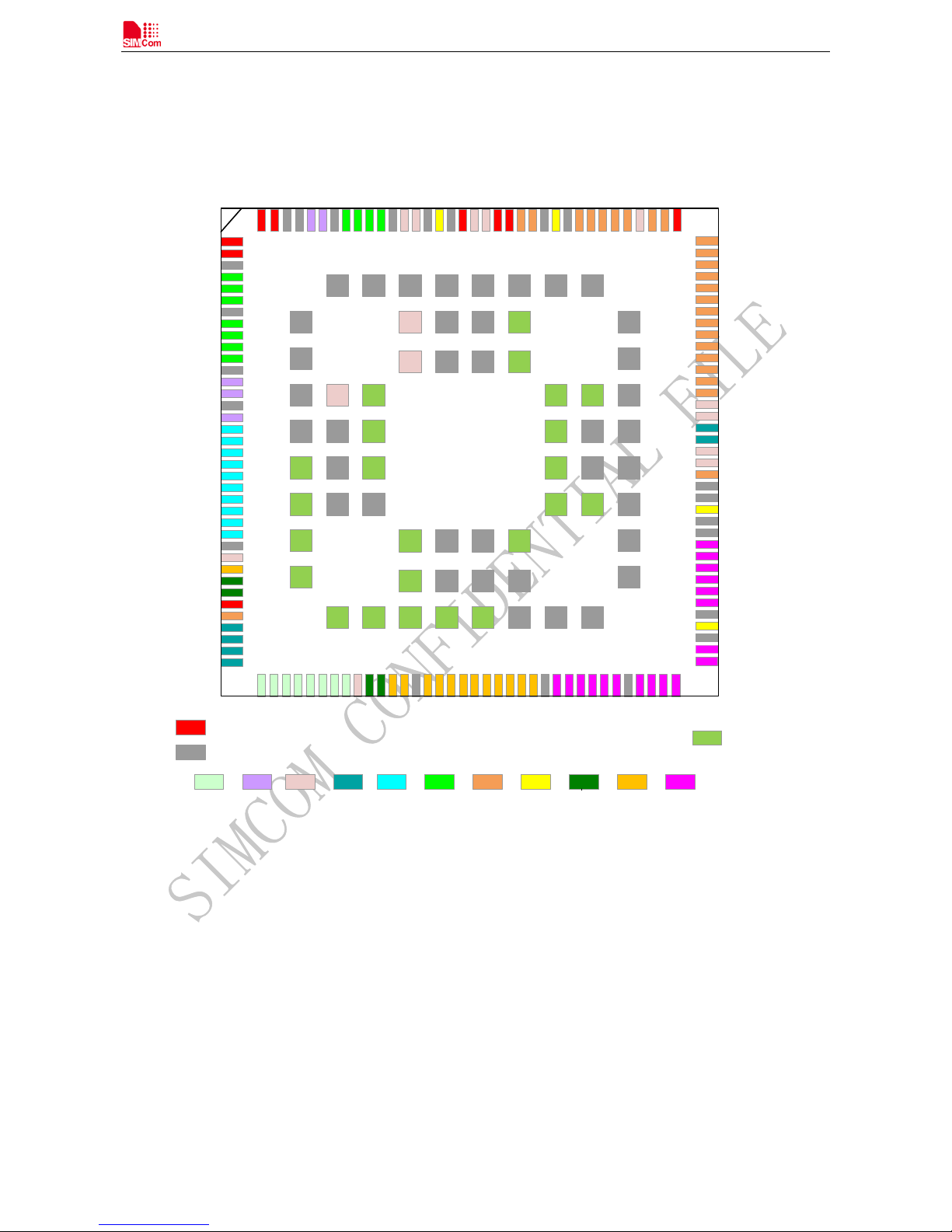
1.3. Pin
99
98
97
96
95
94
93
92
91
90
89
88
87
86
85
84
83
82
81
80
79
78
77
76
75
110
109
108
107
106
105
104
103
102
101
100
111
38
39
40
41
42
43
44
45
46
47
48
49
50
51
52
53
54
55
56
57
58
59
60
61
62
63
64
65
66
67
68
69
70
71
72
73
74
1
2
3
4
5
6
7
8
9
10
11
12
13
14
15
16
17
18
19
20
21
22
23
24
25
26
27
28
29
30
31
32
33
34
35
36
37
115
114
113
112
130
129
128
127
126
125
124
123
122
121
120
119
118
117
116
146
145
144
143
142
141
140
139
138
137
136
135
134
133
132
131
VBAT
_BB
VBAT
_BB
GND
MIC
1P
GND
_
MIC
MIC2P
GND
EAR_
P
SPK_M
SPK_
P
USIM
1
_
RST
USIM1_
CLK
SD
_LDO12
GPIO_23
TP_
RST_N
USB_
DP
GND
USB
_
DM
GND
USIM
1_VDD
GND
USIM1_
DET
PWM
TP_
INT_N
USIM1
_DATA
USB_
ID
USIM
2
_DET
USIM
2
_
RST
USIM
2
_CLK
VIB
_
DRV
_
N
USIM2_DATA
USIM
2_
VDD
ALSP
_INT
_
N/
GPIO
_94
GPIO
_98
GPIO_0
GPIO_
110
GPIO
_
97
GPIO_68
GPIO
_69
GPIO_
89
GPIO
_
88
GPIO
_92
GPIO
_31
KEY
_VOL
_DOWN
_
N
CAM0_RST
_N
UART
2
_
TXD
SENSOR
_
I2
C_
SDA
SENSOR_I
2C
_
SCL
GND
ANT_
MAIN
GPIO
_32
UART2
_
RXD
KEY_
VOL
_UP
_N
CAM0_
PWDN
GND
GND
ANT-BT
GND
CAM
1_
MCLK
HPH_GND
HPH
_R
HS_DET
HPH_L
USB_VBUS
GND
GND
VBAT_
THERM
VBAT_
SNS
GND
ANT_
DRX
GND
LDO17_
2V85
ADC
CHARGE_SEL
VRTC
ANT_GNSS
GND
GPIO
_8
GND
LDO6_1
V8
GPIO_17
GPIO_16
GPIO_
95
SD
_DATA1
SD_
DATA2
SD_
DATA3
SD_CLK
SD_CMD
SD_DATA0
SD_DET
/GPIO_38
TP_
I2C_SCL
TP_I2
C_SDA
SD
_LDO11
LCD_
RST_N
LCD_TE
GND
MIPI_DSI
_CLK_
M
MIPI_DSI_
CLK_P
MIPI_DSI_
LANE0M
MIPI_DSI
_LANE0
P
GND
MIPI_CSI
0_CLK_M
USB
_BOOT
SIM8905
UART1
_CTS
UART
1_RTS
UART
1_
RXD
UART1
_
TXD
MIPI
_DSI_LANE3
P
MIPI_
DSI_LANE3M
MIPI_DSI_
LANE2P
MIPI
_DSI_LANE
2M
MIPI_
DSI_LANE
1P
MIPI
_DSI_
LANE1M
MIPI
_CSI0_
LN1_
P
MIPI_
CSI0_
LN1_
M
MIPI
_CSI0
_LN0_
P
MIPI_CSI
0_LN
0_M
MIPI_CSI
0_CLK
_P
MIPI
_CSI
1_CLK
_M
MIPI_CSI
1_CLK
_P
MIPI
_CSI1
_LN0
_M
MIPI_CSI1
_LN0
_P
GND
CAM0
_MCLK
GND
CAM_
I
2
C
_SDA
CAM
_I2
C_SCL
CAM
1
_
PWDN
CAM1_
RST_N
ACCL
_
INT2
_
N/
GPIO_
65
MAG
_INT
_
N/
GPIO_36
LDO
5
_1V8
ACCL
_
INT1
_
N/
GPIO_
96
PWRKEY
GPIO_
99
GPIO_58
GPIO_
9
GPIO_10
GPIO_
11
VBAT_RF
VBAT_RF
GND
GND
USB
_VBUS
147
EAR_
M
GND
148
149
150
151
152
153
154
179
180
181
182
195
196
197
198
163
164
165
166
167
168
169
170
187
188
189
190
203
204
205
206
171
172
173
174
175
176
177
178
191
192
193
194
207
208
209
210
155
156
157
158
159
160
161
162
183
184
185
186
199
200
201
202
RESERVED
POWER
SDC2
USB
Others
UART
USIM
AUDIO
GND
GPIO
Antenna
TP
LCM
Camera
RESET
MIC
_
BIAS
1
MIC_BIAS2
Page 6
Smart Machine Smart Decision
6
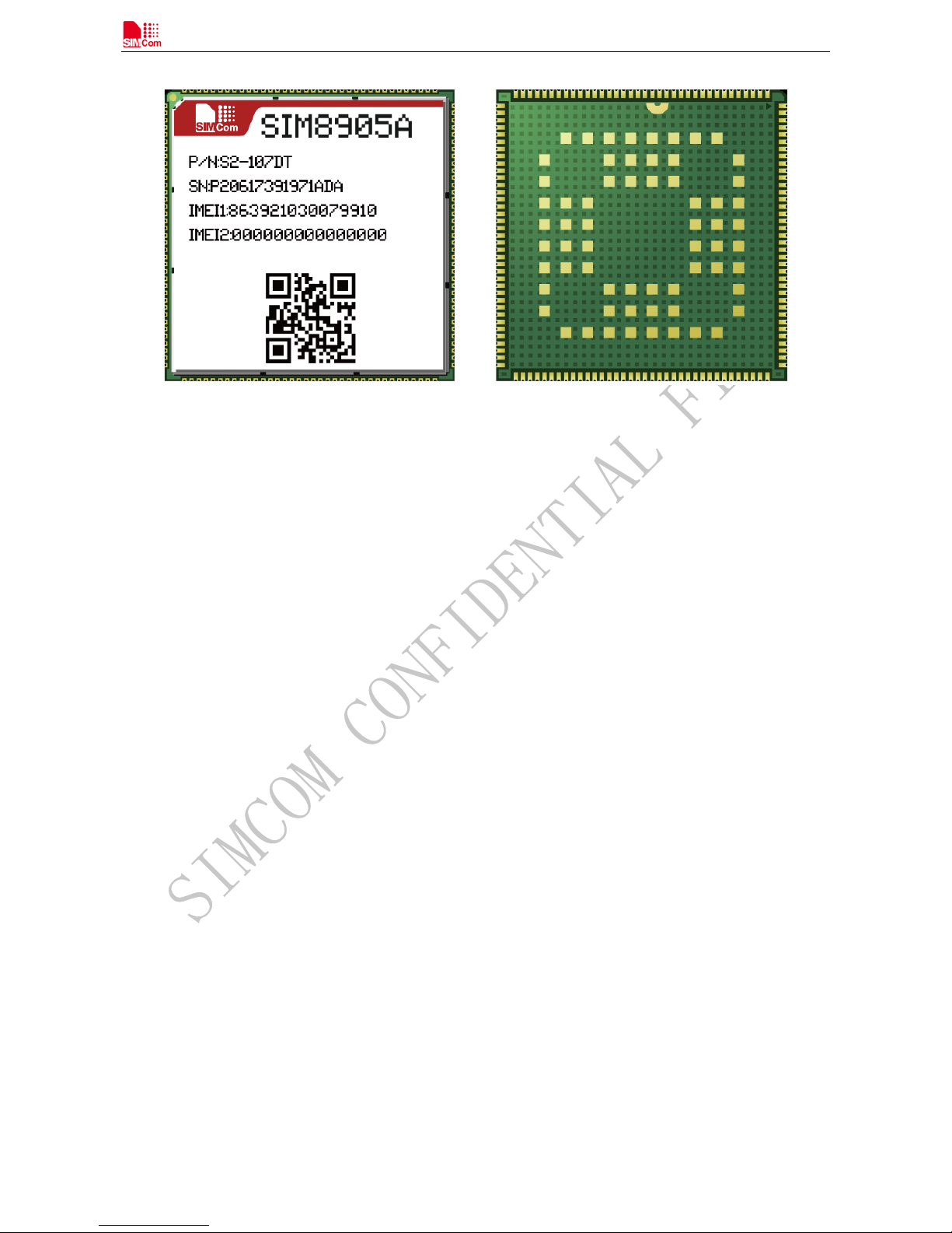
1.4. Picture
Figure 1: T op and Bottom view of SIM8905A
Page 7
Smart Machine Smart Decision
7
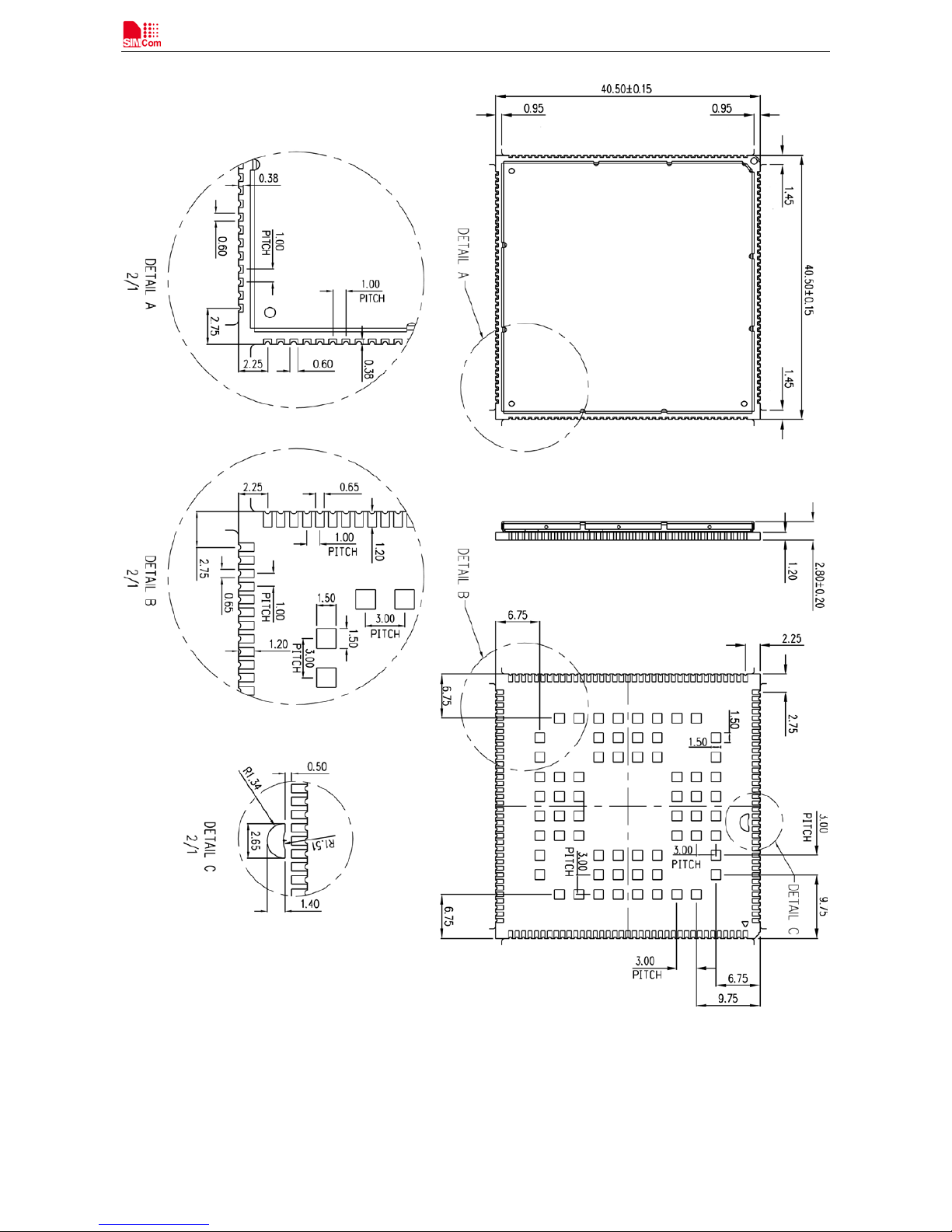
1.5. Dimension
Figure 2: Dimention
Page 8
Smart Machine Smart Decision
8
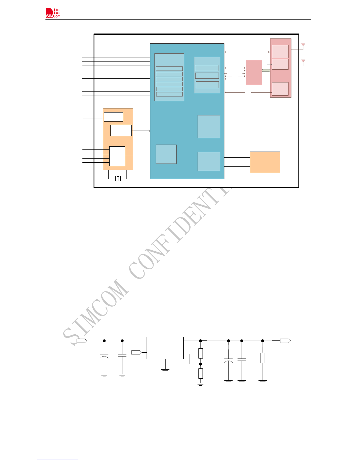
2. Detail Block Diagram
MSM8909
eMMC flash +
LPDDR3
EBI1
SDC1
GPIO
Keypad Buttons
I2C
SPI
UART * 2
4 Lanes DSI
2 Lanes CSI
1 Lanes CSI
USB
UIM1
UIM2
SDC2
Earpiece
Microphone
Headset
TP/Sensor/Cam/others
Vibrator
Keypad Buttons
CODEC
Linear
Charger
Output Power
Management
PM8909
19.2M XO
PDM BUS
Primary Camera (8MP)
720P LCD
Secondary Camera (5MP)
USB HS (Support OTG)
UIM Card2
SD Card
UIM Card1
VBUS_5V
VBAT
ADC
Speaker
4G/3G/2G MODEM
Core
MODEM/Voice
Processor
GNSS
Baseband
Modem
Jolokia
WWAN RX I/Q
GSM Phase
WWAN TX I/Q
RFFE
GNSS I/Q
WTR4905
Front End
MMMB
Power
Amplifier
Modele
RFFE
RFFE
3rd party
PA+SW
DIVERSITY
SWITCH
MODULE
MAIN
DRX
BT/WIFI
Baseband
Codec Digital
AP
Quad A7 w/ 512K L2
Camera ISP/VFE/Jpeg HW
Display Processor
Video
Graphics
Peripherals
SPMI BUS
Memory Support
Note2
Figure 3: Block diagram of SIM8905A
3. Interface Application
Power Supply
The power supply pins of SIM8905A include VBAT_RF and VBAT_BB. VBAT_RF directly supplies the power
t o R F PA ; VBAT_BB supplies the power to the baseband system. The power supply of SIM8905A ranges from
3.4V to 4.4V, and 3.9V is recommended. It must be able to provide sufficient current up to 3A for the high-power
transmitting.
If the DC input voltage is +5V and customers do not care about the power efficiency, a high-current low-dropout
regulator is recommended. Figure 4 is the reference design.
Vin
Vout
GND
FB
3
+
PWR_CTRL
R102
R101
VBAT
100K
47K
+
C103
330uF
C104
100nF
U101
MIC29302
5
4
1
2
C101 C102
100uF
1uF
DC INPUT
R103
470R
On/Off
Figure 4: LDO power supply reference circuit
Note: To ensure a proper behavior of the regulator under light load, an extra minimum load (R103 in Figure 4)
is required, because the current SIM8905A consumed is very small in sleep mode and power off mode. For
more details about minimum load, please refer to specification of MIC29302.
Page 9
Smart Machine Smart Decision
9
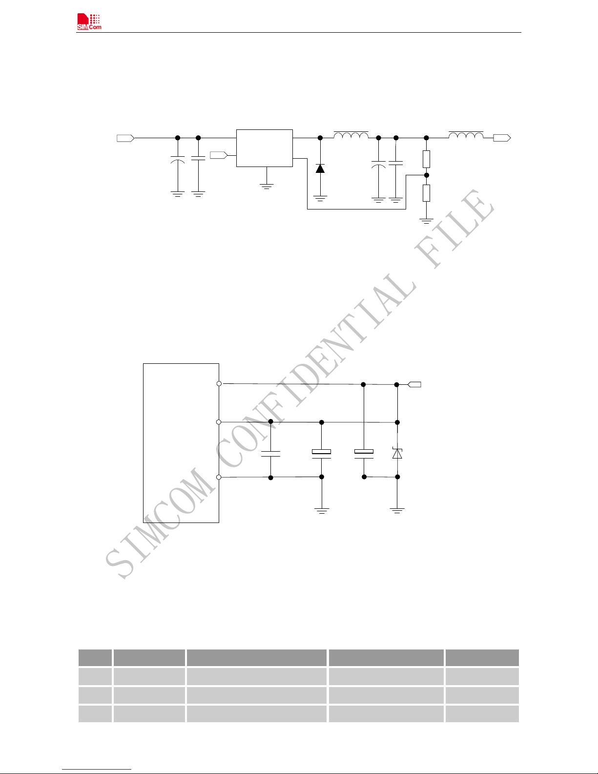
To increase power efficiency, the switching mode DC-DC converter is preferable, especially when DC input
voltage is quite high. The following figure is the reference design, and it is recommended to reserve a proper
ferrite bead (FB101 in Figure 5) in series for EMI suppression.
Vin
Vout
FB
U101
1
2
3
4
5
LM2596-ADJ
+
100uH
MBR360
L101
C101
+
C102
D102 C103
R102
R101
FB101
330uF
VBAT
2.2K
1K
100uF
1uF
C104
100nF
270R@100MHz
DC INPUT
PWR_CTRL
GND
On/Off
Figure 5: DC-DC power supply reference circuit
For battery-powered application, the 3.7V lithium battery can be connected to SIM8905A VBAT pins directly, but
other types of battery must be used carefully, since their maximum voltage may rise over the absolute maximu m
voltage of the module. When battery is used, the total impedance between battery and VBAT pins should be less
than 150mΩ.
In any case mentioned above, at the VBAT input pins side, please take Figure 6 as a reference:
5.1V
500mW
33pF
VBAT
VBAT_BB
GND
C101
C103
100uF
Module
D101
C105
220uF
VBAT_RF
Figure 6: VBAT input reference circuit
Where C101 is a 100uF tantalum capacito r with low ESR; C105 is a 220uF tantalum capacitor with lo w ESR;
33pF and 10pF capacitors are used for eliminating the high frequency interference; 5.1V/500mW zener diode can
protect the module against voltage surge.
All of these components should be placed as close to VBAT pins as possible.
Table 1: Recommended zener diode
Vendor
Part number
Power(watts)
Packages
1
On semi
MMSZ5231BT1G
500mW
SOD123
2
Prisemi
PZ3D4V2H
500mW
SOD323
3
Vishay
MMSZ4689-V
500mW
SOD123
Page 10
Smart Machine Smart Decision
10
4
Crownpo
CDZ55C5V1SM
500mW
0805
Power on/off
Power on
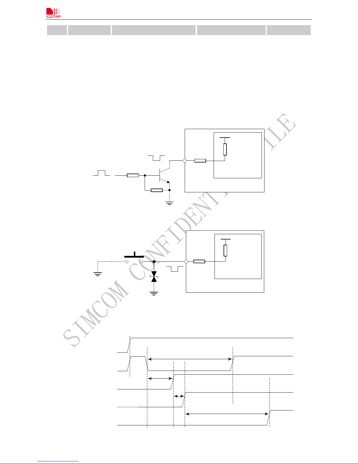
Users can power on SIM8905A by pulling down the PWRKEY pin for more than 2 second then release. This pin
is already pulled up to 1.8V internally, so external pull up is not necessary. Reference circuits are shown as below:
4.7K
47K
PWRKEY
R
1.8V
1K
PMU
Module
Figure 7: Powered on/down module using transistor
PWRKEY
1
K
Module
R
1.8V
PMU
Figure 8: Powered on/down module using button
The power on sequence is illustrated in Figure9
Software Controlled
VBAT
PWRKEY
Others
t>2s
LDO5_1V8
LDO6_1V8
250us
175ms
Page 11
Smart Machine Smart Decision
11
Figure9: Timing of power on module
Power off
Users can power off SIM8905A by pulling down the PWRKEY pin for more than 8 seconds.
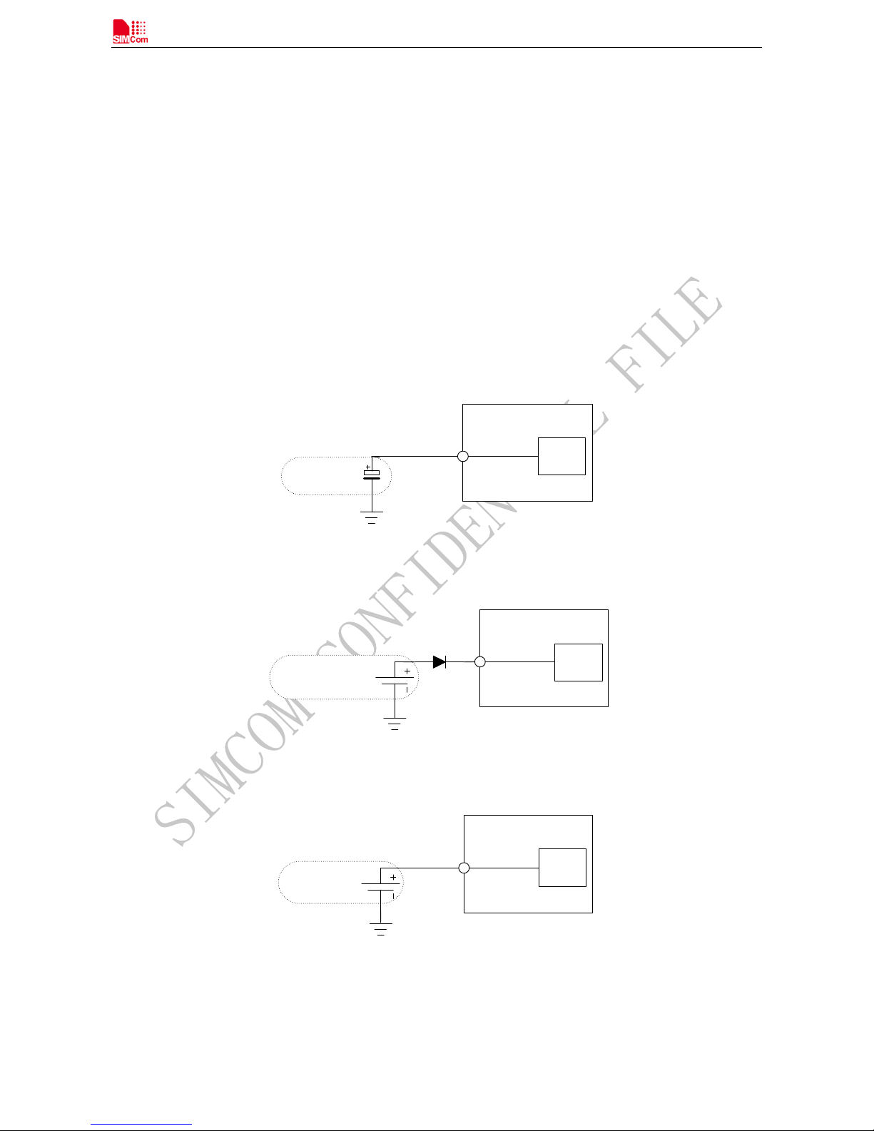
VRTC
VRTC is the power supply for RTC circuit and charger output for coin cell or backup battery. If RTC support is
needed when the battery is removed, a qualified coin cell or keep-alive capacitor is required on the VRTC pin.
When VBAT is present and valid, coin cell charging is enabled through software control and powered from VBAT.
Reference circuits are shown as below:
Keep-alive capacitor:
RTC
Module
VRTC
Capacitor
Figure 10: Keep-alive capacitor
Non-rechargeable battery:
RTC
Module
VRTC
Non-rechargeable
battery
Figure 11: Non-rechargeable battery
Rechargeable battery:
RTC
Module
VRTC
Rechargeable
battery
Figure 12: Rechargeable battery
VRTC typical voltage is 3.0V, and the current consumption is about 5uA when VBAT is absence. For electrical
characteristics, please refer to Table 23: VRTC characteristic.
Page 12
Smart Machine Smart Decision
12
Output Power Management
Table 2: Output power management summary
Pin Name Pin# Specified range (V) Rated current (mA) Expected use
LDO5_1V8
111
1.8 50 Force USB boot
LDO6_1V8
125
1.8
200
Display, camera, sensors
SD_LDO11
38
2.95
600
SD/MMC card
SD_LDO12
32
1.8/2.95
50
For SD signals pull-up
USIM1_VDD
26
1.8/2.95
50
USIM 1
USIM2_VDD
21
1.8/2.95
50
USIM 2
LDO17_2V85
129
2.85
420
Display, camera, sensors
USB Interface
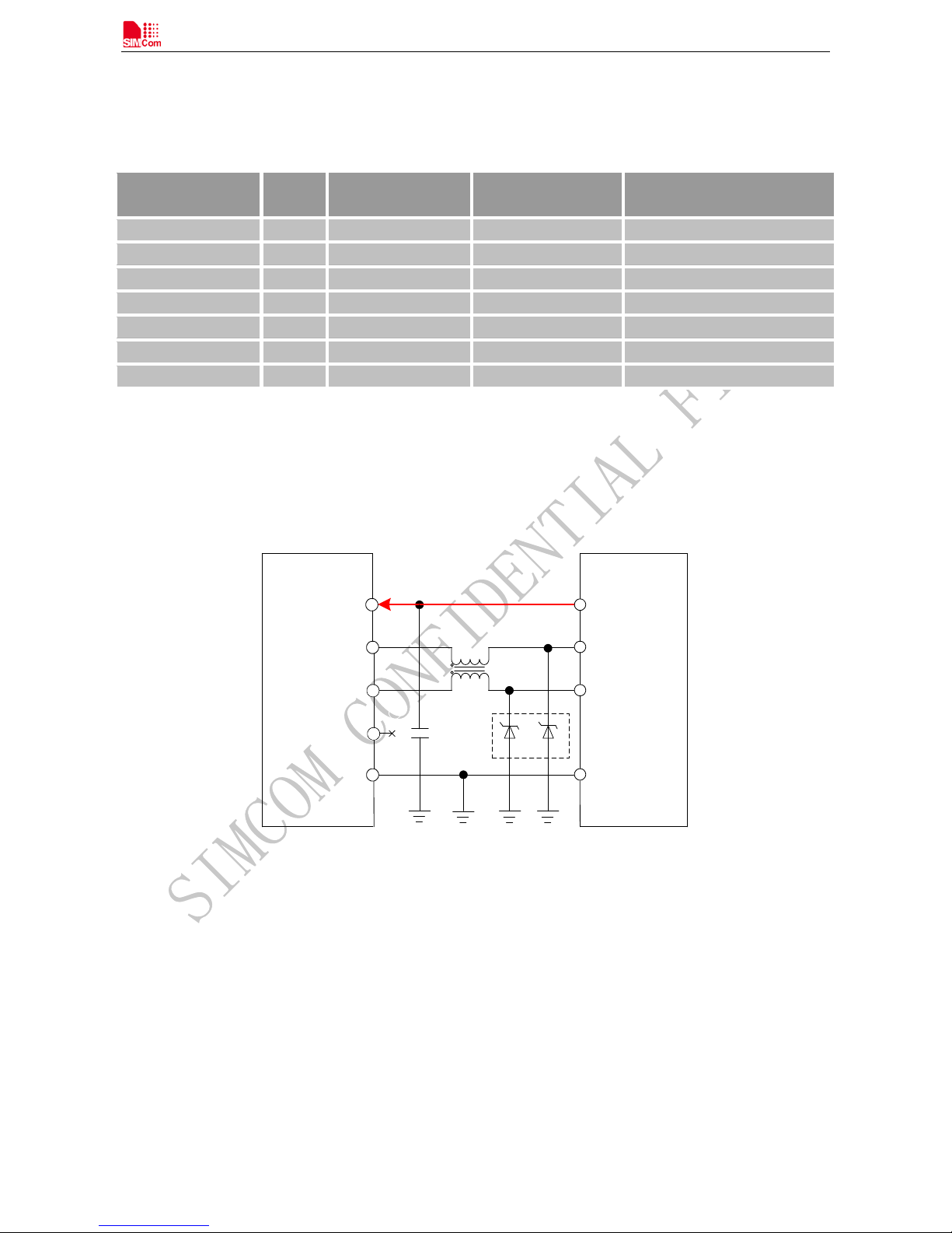
SIM8905A provides one High-speed USB 2.0 interface, used for software upgrading, debugging, charging, etc.
Module
Connector
USB_DM
GND
GND
USB_VBUS
VBUS
1uF
<1pF
USB_DP
USB_DM
USB_DP
USB_ID
Figure 13: USB reference circuit
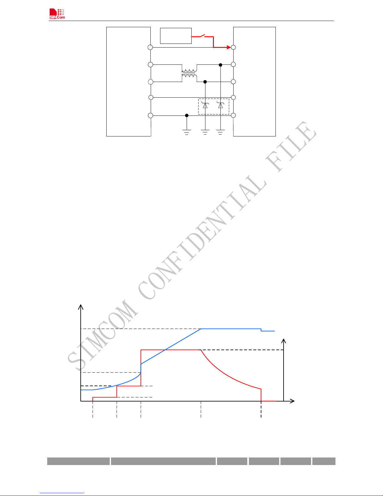
In addition, SIM8905A supports OTG function, but external 5V power supply is required.
Page 13
Smart Machine Smart Decision
13
Module
Connector
USB
_
DM
GND
GND
USB
_
VBUS
VBUS
<1pF
USB_DP
USB_
DM
USB
_ID
USB
_
ID
USB
_
DP
External 5
V
Figure14: USB_OTG reference circuit
Linear Battery Charger
SIM8905A module integrates a 1.44A linear battery charger for single-cell lithium-ion batteries.
Charging Control
Battery charging is controlled by a PMIC state-machine. The first step in the automated charging process
determines if trickle charging is needed. Charging of a severely depleted battery must begin with trickle charging
to limit the current, avoid pulling VDD down, and protect the battery from more charging current than it can
handle. Once a minimum battery voltage is established using trickle charging, constant-current charging is enabled
to charge the battery quickly – this mode is sometimes called fast charging. Once the battery approaches its target
voltage, the charge is completed using constant-voltage charging.
V
WEAK
V
TRKL
3
.2V
2.8V
V
BAT
V
BAT-MAX
4.2V
450mA
/1440mA
I
BAT
I
BAT-MAX
Time
TRKL-A T
RKL-B CC CV
I
TRKL-A
90mA
I
TRKL-B
450
mA
Figure15: Charging control diagram
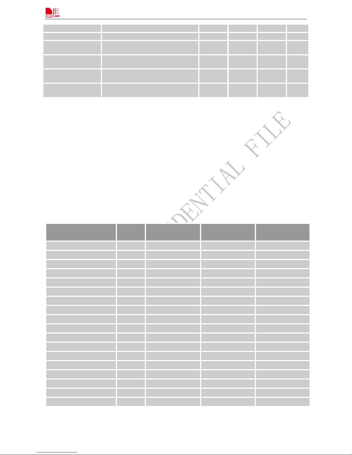
Table 3: Linear battery charger performance specifications
Parameter
Comments
Min
Typ
Max
Units
Page 14
Smart Machine Smart Decision
14
I
TRKL-A
Trickle-A Charging current
81
90
99
mA
I
TRKL-B
Trickle-B Charging current
405
450
495
mA
V
TRKL
Trickle-B threshold voltage range
Programmable, 15.62 mV steps
2.5 2.796 2.984 V
V
WEAK
Weak battery threshold range
Programmable, 18.75 mV steps
3.0 3.206 3.581 V
V
BAT_M A X
Maximum battery voltage
Programmable, 25 mV steps
4 4.2 4.775 V
I
BAT_M AX
Fast charging current range
Programmable, 90mA steps
90 1440 mA
VBAT_SNS
VBAT_SNS is used for battery voltage sensing, the typical input range is 2.5V~4.5V.
UART/SPI/I2C
SIM8905A provides several sets of GPIOs which are available as BLSP (BAM-enabled low-speed peripheral)
interfaces that can be configured to support various interface combinations, as shown in the following table. T he
operation voltage is 1.8V
Table 4: UART/SPI/I2C functional assignments
Pin Name Pin#
Expected or Default
Function
Alternative
Function 1
Alternative
Function 2
UART2_TXD
94
BLSP1_UART_TX
BLSP1_SPI_MOSI
UART2_RXD
93
BLSP1_UART_RX
BLSP1_SPI_MISO
SENSOR_I2C_SDA
92
BLSP1_I2C_SDA
BLSP1_SPI_CS_N
BLSP1_UART_CTS
SENSOR_I2C_SCL
91
BLSP1_I2C_SCL
BLSP1_SPI_CLK
BLSP1_UART_RTS
GPIO_8
119
GPIO
BLSP6_SPI_MOSI
GPIO_9
118
GPIO
BLSP6_SPI_MISO
GPIO_10
117
GPIO
BLSP6_SPI_CS_N
BLSP6_I2C_SDA
GPIO_11
116
GPIO
BLSP6_SPI_CLK
BLSP6_I2C_SCL
GPIO_16
123
GPIO
BLSP5_SPI_MOSI
GPIO_17
124
GPIO
BLSP5_SPI_MISO
TP_I2C_SDA
48
BLSP5_I2C_SDA
BLSP5_SPI_CS_N
TP_I2C_SCL
47
BLSP5_I2C_SCL
BLSP5_SPI_CLK
UART1_TXD
34
BLSP2_UART_TX
BLSP2_SPI_MOSI
UART1_RXD
35
BLSP2_UART_RX
BLSP2_SPI_MISO
UART1_CTS
36
BLSP2_UART_CTS
BLSP2_SPI_CS_N
BLSP2_I2C_SDA
UART1_RTS
37
BLSP2_UART_RTS
BLSP2_SPI_CLK
BLSP2_I2C_SCL
CAM_I2C_SDA
84
BLSP3_I2C_SDA
CAM_I2C_SCL
83
BLSP3_I2C_SCL
Note:
1. UART: can be used as a diagnostic port, up to 4 Mbps;
2. I2C: supports master-only mode; up to 3.4 MHz, 2.2Kohm pull -up resistors are needed externally;
Page 15
Smart Machine Smart Decision
15
3. SPI: supports master-only mode; up to 52 MHz.
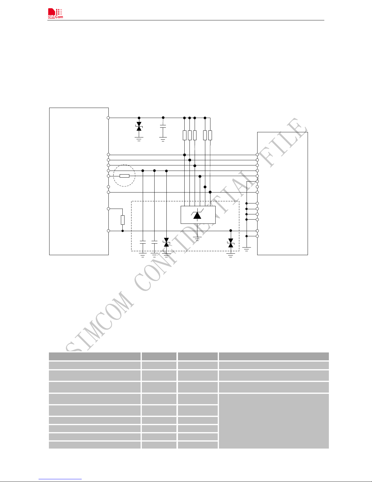
Secure Digital Interface
SIM8905A provides one 4-bit secure digital interface, which supports the following standards:
SD Specifications Part 1 Physical Layer Specification Version 3.00
Part A2 SD Host Controller Standard Specification Version 3.00
Part E1 SDIO Specification Version 3.00
1 DAT2
2 DAT3
3 CMD
4 VDD
5 CLK
6 VSS
7 DAT0
8 DAT1
11 GND
12 GND
13 GND
14 GND
9 DET_SW
10 COMMON
SD Card
SD_DATA2
SD_DATA3
SD_CMD
SD_LDO11
SD_CLK
SD_DATA0
SD_DATA1
1M
SD_DET
LDO5_1V8
Module
1uF
33pF
TVS
C<15pF
Placed close to SD card
33R
33R is required for high-speed operation;
placed close to the module
NMNMNMNMNM
1uF
SD_LDO12
NM:Not Mounting
Reserved
Figure17: SD card reference circuit
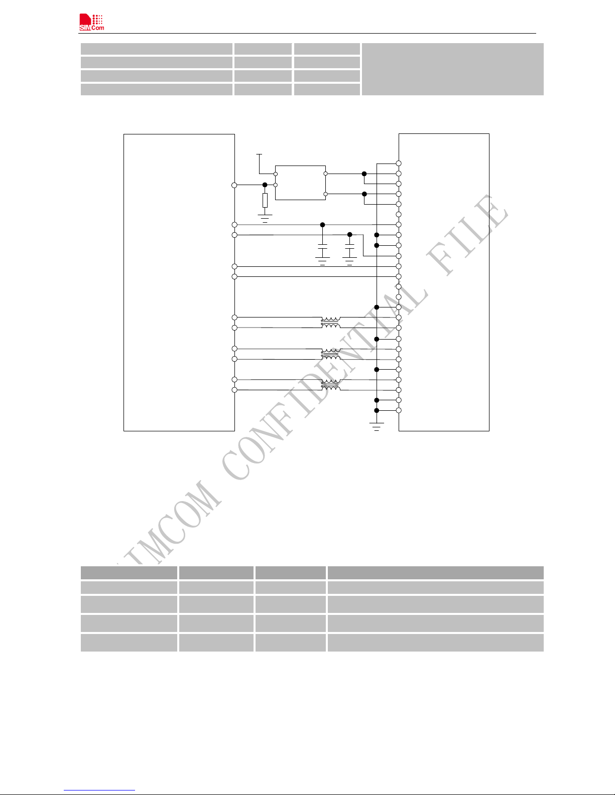
Display Interface
SIM8905A provides a 4-lane MIPI_DS I, with 1.5 G bps per lane high-speed mode bandwidth, to support 720p HD
display.
PWM is used as PWM control for external WLED driver.
Table 5: Display interface pin definitions
Pin Name
Pin#
Type
Description
PWM
29
O
PWM control for external WLED driver
LCD_RST_N
49
O
LCD reset
LCD_TE
50
I
LCD tear effect
MIPI_DSI_CLK_M
52
O
MIPI display serial interface
MIPI_DSI_CLK_P
53
O
MIPI_DSI_LANE0M
54
O
MIPI_DSI_LANE0P
55
O
MIPI_DSI_LANE1M
56
O
MIPI_DSI_LANE1P
57
O
Page 16
Smart Machine Smart Decision
16
If only 2-lane MIPI_DSI is needed, just leave LANE2 and LANE3 floating.
1
GND
2 LED
+
3 LED+
4 LED5 LED6 LCD_ID
7
VCC(2.8V)
8 GND
9 GND
10 VCC_IO
11 RESET
12 TE
13 NC
14 NC
15 GND
16 DSI_D117 DSI_D1+
18 GND
19 DSI_CLK20 DSI_CLK+
21 GND
22 DSI
_D0
23 DSI_D0+
24 GND
25 GND
LCM
LED+
LED-
LCD_RST_N
LCD_TE
MIPI_DSI_LANE1_M
MIPI_DSI_LANE1_P
MIPI_
DSI_CLK_M
MIPI_DSI_CLK_P
MIPI_DSI_
LANE0_M
MIPI_DSI_LANE0_P
LDO17_2V85
1uF
1uF
LDO6_1V8
PWM
WLED
driver
VBAT
Module
1
M
Figure 18: Display reference circuit
Touch Screen Interface
Table 6: Touch screen interface pin definitions
Note:
1. TP_I2C: supports master-only mode; 2.2Kohm pull-up resistors are needed externally;
MIPI_DSI_LANE2M
58
O
MIPI_DSI_LANE2P
59
O
MIPI_DSI_LANE3M
60
O
MIPI_DSI_LANE3P
61
O
Pin Name
Pin#
Type
Description
TP_I2C_SDA
48
I/O
Touch screen I2C data
TP_I2C_SCL
47
O
Touch screen I2C clock
TP_INT_N
30
I
Touch screen interrupt
TP_RST_N
31
O
Touch screen reset
Page 17
Smart Machine Smart Decision
17
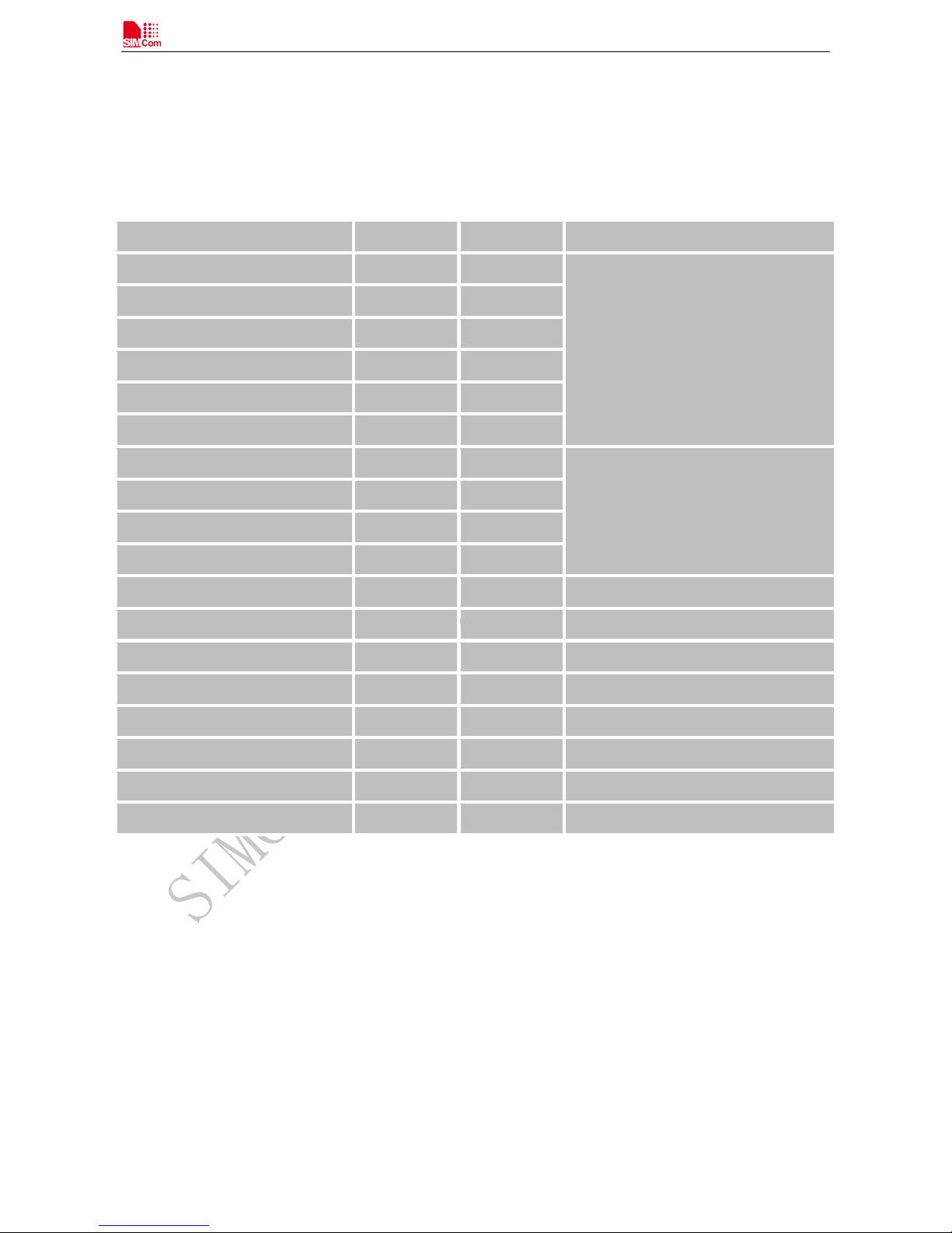
Camera Interface
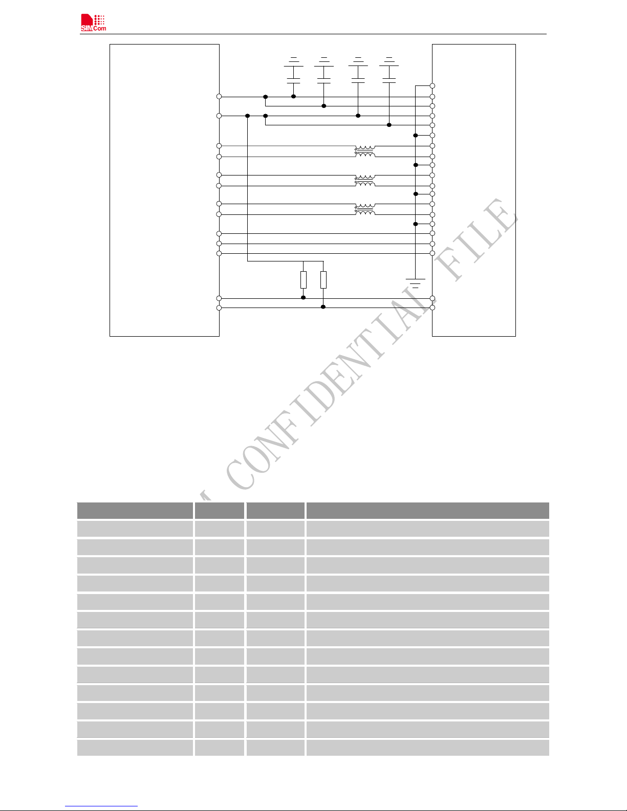
SIM8905A supports two cameras: 2-lane MIPI_ CSI primary camera up to 8MP resolution and 1-lane MIPI_C SI
secondary camera up to 5MP resolution.
Table 7: Camera interface pin definitions
Pin Name Pin# Type Description
MIPI_CSI0_CLK_M
63
I
Primary camera serial interface
MIPI_CSI0_CLK_P
64
I
MIPI_CSI0_LN0_M
65
I
MIPI_CSI0_LN0_P
66
I
MIPI_CSI0_LN1_M
67
I
MIPI_CSI0_LN1_P
68
I
MIPI_CSI1_CLK_M
70
I
Secondary camera serial interface
MIPI_CSI1_CLK_P
71
I
MIPI_CSI1_LN0_M
72
I
MIPI_CSI1_LN0_P
73
I
CAM0_MCLK
74
O
Primary Camera master clock
CAM1_MCLK
75
O
Secondary Camera master clock
CAM0_RST_N
79
O
Primary Camera reset
CAM0_PWDN
80
O
Primary Camera power down
CAM1_RST_N
81
O
Secondary Camera reset
CAM1_PWDN
82
O
Secondary Camera power down
CAM_I2C_SCL
83
O
Camera I2C clock
CAM_I2C_SDA
84
I/O
Camera I2C data
Page 18
Smart Machine Smart Decision
18
LDO17_2V85
LDO6_1V8
AGND
VCM
AVDD
DVDD
VDD_IO
GND
MCP
MCN
GND
MDP0
MDN0
GND
MDP1
MDN1
GND
MCLK
RESET
PWDN
MIPI_CSI
0_CLK_P
MIPI_CSI0_CLK_M
MIPI_CSI0_LN0_P
MIPI_CSI0_LN0_M
MIPI_CSI0_LN1_P
MIPI_CSI0_LN1_M
CAM0_MCLK
CAM0_RST_N
CAM0_PWDN
100nF 100nF2.2uF
Primary
Camera
Module
2.2uF
2.2K
2.2K
CAM_I2C_SCL
CAM_I2C_SDA
SCL
SDA
Figure 19: Primary camera reference circuit
Audio
SIM8905A provides two microphone inputs and three outputs including earpiece, stereo headphones, and mono
class-D speaker driver.
Table 8: Audio interface pin definitions
Pin Name Pin# Type Description
EAR_P 8 O
Earpiece output, positive
EAR_M 9 O
Earpiece output, negative
HPH_R
136
O
Headphone output, right channel
HPH_GND
137
I
Headphone ground reference
HPH_L
138
O
Headphone output, left channel
HS_DET
139
I
Headset detection
GND_MIC
5
P
Microphone input 2 ground reference
MIC2P 6 I
Microphone input 2, positive
MIC1P 4 I
Microphone input 1, positive
SPK_M
11
O
Speaker driver output, negative
SPK_P
10
O
Speaker driver output, positive
MIC_BIAS1
194
O
Microphone bias 1
MIC_BIAS2
210
O
Microphone bias 2
Page 19
Smart Machine Smart Decision
19
Microphone
Electret
Microphone
route as differential pair
& shielded by GND
Close to microphone
MIC1P
Module
GND_MIC
ESD
ESD
10pF
33pF
33pF
33pF
10pF
10pF
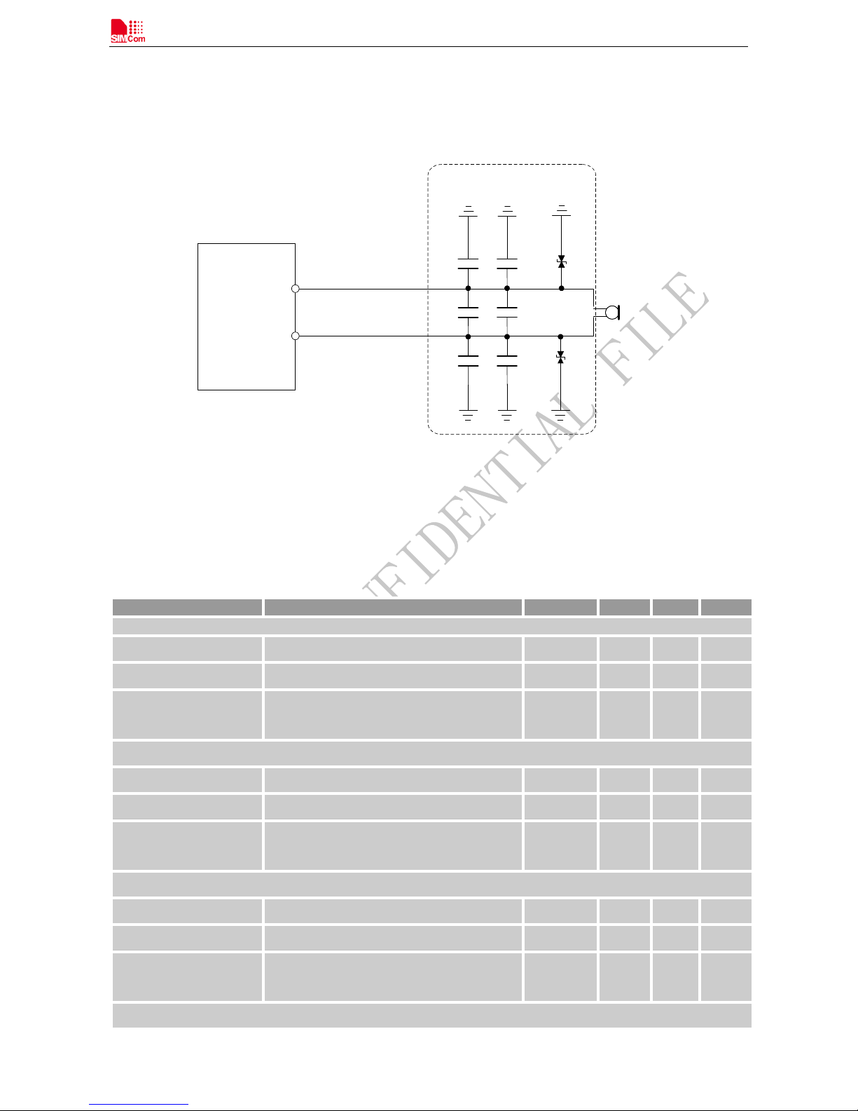
Figure 20: Microphone reference circuit
Note:
1. Internal MIC_BIAS pull-up is used to reduce BOM cost and PCB routing.
2. Single-ended capless input is the only supported configuration, but differential routing is recommended.
Table 9: Analog microphone input performance
Parameter
Test conditions
Min
Typ
Max
Units
Microphone amplifier gain = 0 dB (minimum gain)
Input referred noise
Single-ended, A-weighted, capless
-
19.3
25.1
µVrms
Signal-to-noise ratio
Single-ended, A-weighted, capless
92.0
94.0 - dB
THD+N ratio
Analog input = -1 dBV
f = 1.02 kHz; single-ended input; 200 Hz to
20 kHz bandwidth; capless
-
-86.0
-70.0
dB
Microphone amplifier gain = 6 dB
Input referred noise
Single-ended, A-weighted, capless
-
5.9
7.1
µVrms
Signal-to-noise ratio
Single-ended, A-weighted, capless
91.0
92.5 - dB
THD+N ratio
Analog input = -1 dBV
f = 1.02 kHz; single-ended input;
200 Hz to 20 kHz bandwidth; capless
-
-85.0
-70
dB
Microphone amplifier gain = 24 dB (maximum gain)
Input referred noise
Single-ended, A-weighted, capless
-
3.4
4.2
µVrms
Signal-to-noise ratio
Single-ended, A-weighted, capless
84.2
85.4 - dB
THD+N ratio
Analog input = -1 dBV
f = 1.02 kHz; single-ended input;
200 Hz to 20 kHz bandwidth; capless
-
-82.4
-76.0
dB
General requirements
Page 20
Smart Machine Smart Decision
20
Full-scale input voltage
Single-ended 1 kHz input. Input signal
level required to get 0 dBFS digital output
-0.5
0
0.5
dBV
Input impedance
Capless input
Input disabled
1.0
3.0
-
-
-
-
MΩ
MΩ
Input capacitance
Capless input
- - 15
pF
Headset
Stereo class-AB headphone supports 16 Ω, 32 Ω, and up to 50 KΩ loads. Its typical output power at 1.02 KHz and
THD + N ≤ 1% is:
21.5 mW with 16 Ω loads, 0 dBFS and -4.5 dB gain
30.8 mW with 32 Ω loads, 0 dBFS and 0 dB gain
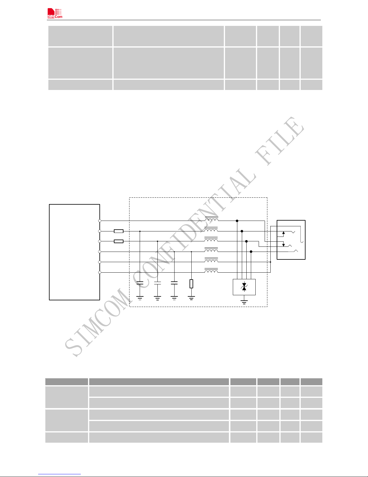
A 100KΩ pull-down resistor is integrated at HPH_L pin, which could be used for mechanical insertion or removal
detection through HS_DET pin. Figure 22 shows the reference circuit for normally-closed (NC) type headset jack.
HPH_R
Module
HPH_L
0R
0R
HS_DET
MIC2P
GND_MIC
HPH_GND
100K
33pF 33pF
33pF
Headset Jack
TVS
Close to headset jack
1000 OHM@100MHZ
1000 OHM@100MHZ
1000 OHM@100MHZ
1000 OHM@100MHZ
1000 OHM@100MHZ
1000 OHM@100MHZ
Figure 21:
Headset reference circuit
Note:
1. SIM8905A also supports NO/NC type headset jack with detect pin on HPH_L or GND.
2. HPH has a negative swing and requires a bi-dir ectional TVS diode.
Table 10: Headphone output performance specifications
Parameter
Test conditions
Min
Typ
Max
Units
Output power
16 Ω load f = 1.02 kHz, 0 dB FS; VDD_CP* = 1.95 V
15.6
21.5
25.5
mW
32 Ω load f = 1.02 kHz, 0 dB FS; VDD_CP* = 1.95 V
27.0
30.8
32.0
mW
Full-scale
output Voltage
16 Ω load f = 1.02 kHz, 0 dB FS; VDD_CP* = 1.95 V
0.50
0.59
0.64
Vrms
32 Ω load f = 1.02 kHz, 0 dB FS; VDD_CP* = 1.95 V
0.96
0.99
1.00
Vrms
Output load
13.0
16/32 - Ω
Page 21
Smart Machine Smart Decision
21
Disabled output
impedance
Measured externally, with amplifier disabled
1.0 - -
MΩ
Note: The VDD_CP is internal Voltage of module.
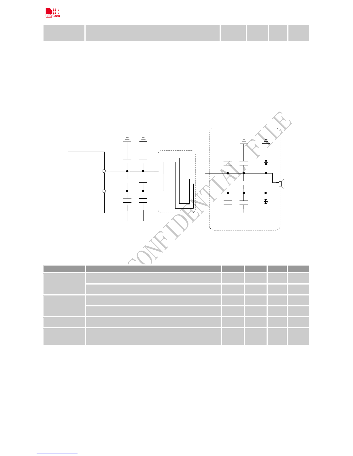
Earpiece
Class AB earpiece driver supports 10.67 Ω, 16 Ω, 32 Ω, and up to 50 KΩ loads. It s typical output power at 1.02
KHz, 6 dB gain, and THD + N ≤ 1% is:
119 mW with 32 Ω loads
243 mW with 16 Ω loads
320 mW with 10.67 Ω loads
EAR_P
Close to earpiece
ESD
ESD
10pF
33pF
33pF
33pF
Module
EAR_M
10pF
10pF
10pF
33pF
33pF
33pF
10pF
10pF
Route as differential pair
& shielded by GND
Figure 22: Earpiece reference circuit
Table 11: Earpiece output performance specifications
Parameter
Test conditions
Min
Typ
Max
Units
Output power
32 Ω load f = 1.02 kHz, 6 dB gain THD+N < 1%
120.0
124.5
-
mW
16 Ω load f = 1.02 kHz, 6 dB gain THD+N < 1%
235.0
243.0
-
mW
Full-scale
output Voltage
6 dB gain mode f = 1.02 kHz
1.8
2.0
2.1
Vrms
1.5 dB gain mode f = 1.02 kHz
1.0
1.2
1.3
Vrms
Output load
10.7
32 - Ω
Disabled output
impedance
Measured externally, amplifier disabled
1.0 - -
MΩ
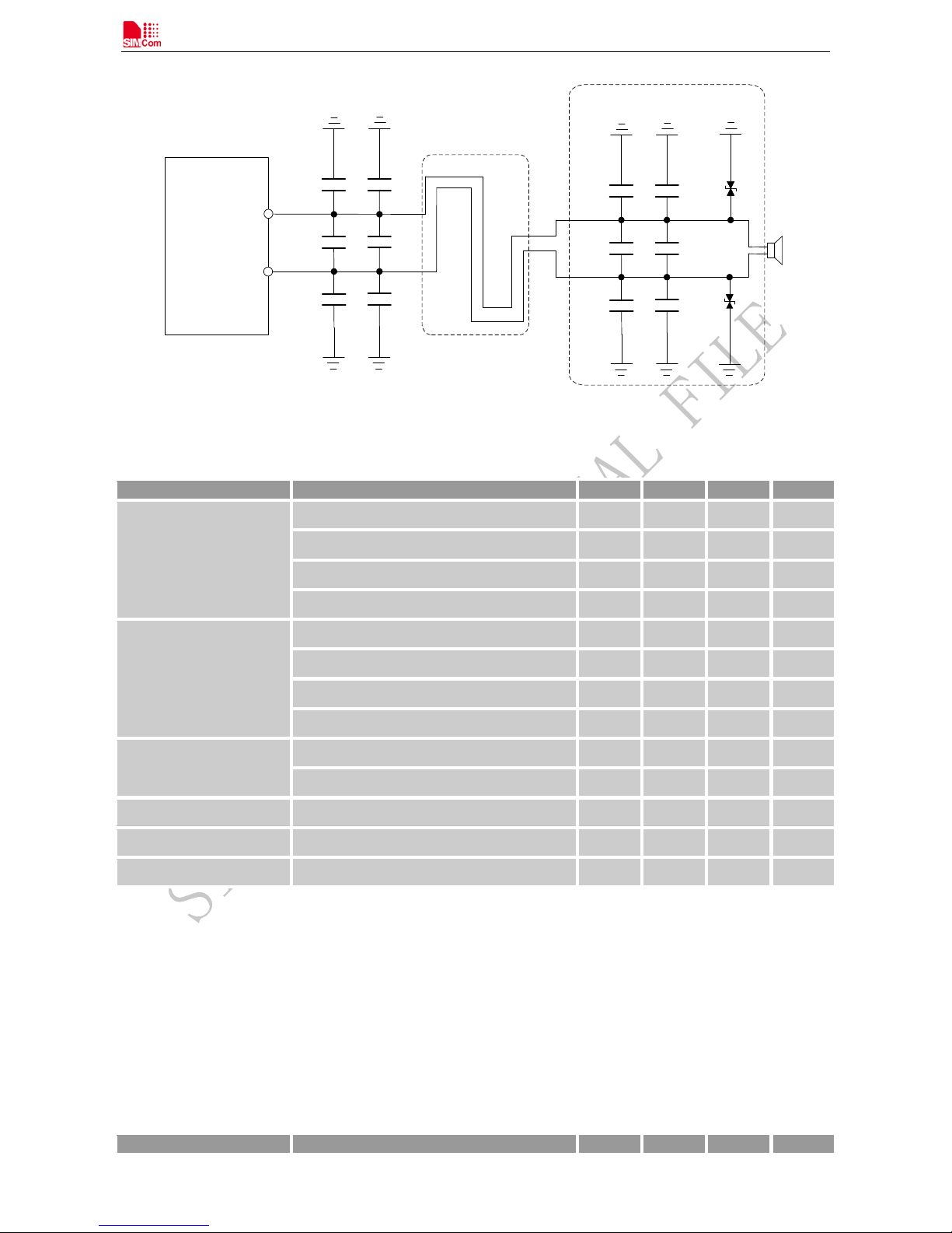
Speaker
Class-D mono differential loud speaker driver supports 4 Ω and 8 Ω loads. The driver is powered from VBAT, and
does not support external 5 V Boost Option. Its typical output power at 1.02 KHz, 12 dB gain, and THD + N ≤
1% is:
950 mW with 8 Ω loads, VDD_SPKR=VBAT= 4.2 V
692 mW with 8 Ω loads, VDD_SPKR= VBAT= 3.6 V
1063 mW with 4 Ω loads, VDD_SPKR=VBAT= 3.6 V
Page 22
Smart Machine Smart Decision
22
SPK1P
Close to speaker
ESD
ESD
10pF
33pF
33pF
33pF
Module
SPK1N
10pF
10pF
10pF
33pF
33pF
33pF
10pF
10pF
Route as differential pair
& shielded by GND
Figure 23: Speaker reference circuit
Table 12: speaker driver output performance specifications
Parameter
Test conditions
Min
Typ
Max
Units
Output power (Pout)
(f = 1 kHz, gain = 12 dB,
THD+N ≤ 1%)
15 μH + 8 Ω + 15 μH, Vdd = 3.6 V
584
631 - mW
15 μH + 4 Ω + 15 μH, Vdd = 3.6 V
862
953 - mW
15 μH + 8 Ω + 15 μH, Vdd = 3.8 V
662
710 - mW
15 μH + 8 Ω + 15 μH, Vdd = 4.2 V
819
879 - mW
THD+N
(1 kHz)
1 W Pout, VDD_SPKR = 4.2 V
-
-85.0
-75.0
dB
800 mW Pout, VDD_SPKR = 4.2 V
-
-75.0
-45.0
dB
600 mW Pout, VDD_SPKR = 3.8 V
-
-75.0
-70.0
dB
500 mW Pout, VDD_SPKR = 3.6 V
-
-76.0
-71.0
dB
Efficiency
(Vdd = 3.7 V)
500 mW Pout, 15 μH + 8 Ω + 15 μH
82.0
84.0 - %
1 W Pout, 15 μH + 4 Ω + 15 μH
73.0
78.0 - %
output impedance
Disabled
25 - -
kΩ
Shutdown
current
-
0.1
1.0
µA
Turn on time
- 0.2
10.0
ms
Microphone bias
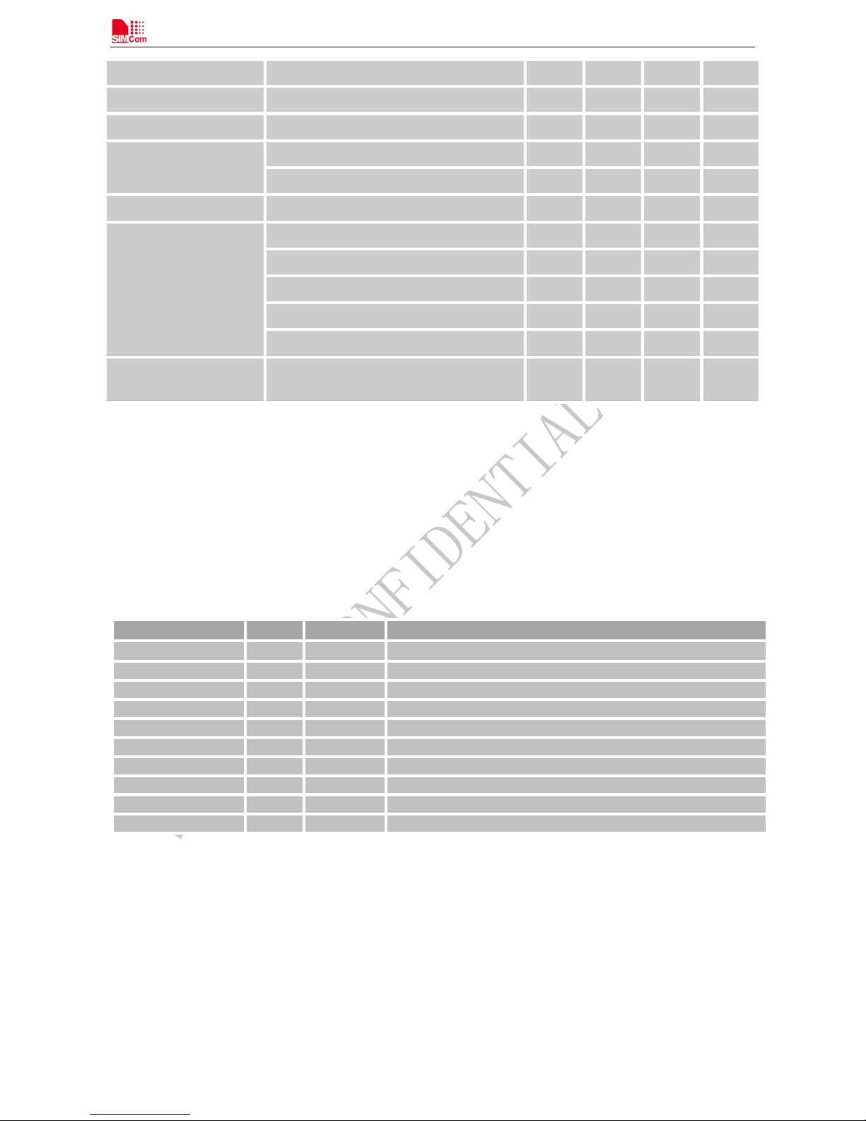
SIM8905A provides two microphone bias outputs: MIC_BIAS1and MIC_BIAS2.
The microphone bias cannot be used for ECM-type microphone. MIC_BIAS1and MIC_BIAS2 could be used
for External MEMS microphone as power supply.
The microphone bias output performance specific ati ons are shown in the following table:
Table 13: Microphone bias output performance specifications
Parameter
Test conditions
Min
Typ
Max
Units
Page 23
Smart Machine Smart Decision
23
Output voltage
No load
1.60 - 2.85
V
Output voltage error
No load
-3.00
0.00
3.00
%
Output current
2 microphone loads of 1.0 to 1.5 mA each
2.0
3.0 - mA
Output switch to ground
On resistance
- - 20
Ω
Sink current
2.0 - -
mA
Output noise
0.1 µF bypass
0.0
2.0
4.0
µVrms
PSRR- Power supply
rejection ratio
at 20 Hz
80 - -
dB
at 200 Hz to 1 kHz
80 - -
dB
at 5 kHz
80 - -
dB
at 10 kHz
80 - -
dB
at 20 kHz
75 - -
dB
Output capacitor value
[2]
External bypass mode[1]
0.1
0.1
0.5
µF
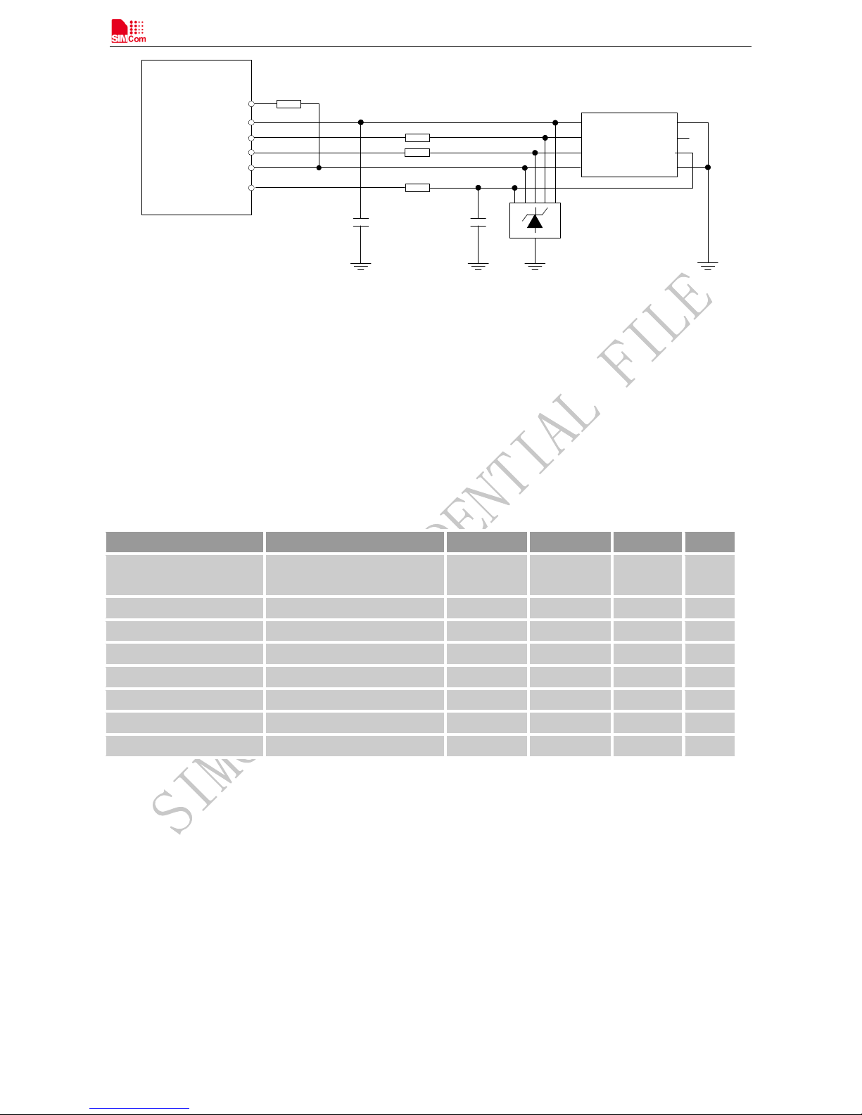
USIM Interface
SIM8905A supports dual cards dual standby, and card presence detection.
Note: The standard software provided by SIMCom only supports single USIM1 card configuration.
Table 14: USIM interface pin definitions
Pin Name
Pin#
Type
Description
USIM2_DET
17
I
USIM2 presence detection
USIM2_RST
18
O
USIM2 reset
USIM2_CLK
19
O
USIM2 clock
USIM2_DAT
20
I/O
USIM2 data
USIM2_VDD
21
P
LDO 15 output for USIM2, 1.8V/2.95V
USIM1_DET
22
I
USIM1 presence detection
USIM1_RST
23
O
USIM1 reset
USIM1_CLK
24
O
USIM1 clock
USIM1_DAT
25
I/O
USIM1 data
USIM1_VDD
26
P
LDO 14 output for USIM1, 1.8V/2.95V
Page 24
Smart Machine Smart Decision
24
Module
DET
22R
220nF
USIM Card
22pF
VCC
GND
RST
VPP
CLK I/O
COM
LDO5_1V8
USIM_VDD
USIM_RST
SUIM_CLK
USIM_DAT
100K
22R
22R
USIM_DET
TVS
C<30pF
Figure 1: USIM card reference circuit
Note:
USIM_DAT has been pulled up with a 10kohm resistor to USIM_VDD in module.
A 220nF shut capacitor on USIM_VDD is used to reduce interference.
ADC
SIM8905A provides one 16bits ADC. Its performance parameters are shown as the following table.
Table 15: ADC performance parameters
Parameter
Comments
Min
Typ
Max
Unit
Input voltage range
Programmable
0.1
0.3
- - 1.7
4.5
V
Resolution
- 16
-
bits
Analog input bandwidth
- 100
-
kHz
Sample rate
XO/8 - 2.4
-
MHz
INL
15-bit output
- - ±8
LSB
DNL
15-bit output
- - ±4
LSB
Offset error
Relative to full-scale
- - ±1
%
Gain error
Relative to full-scale
- - ±1
%
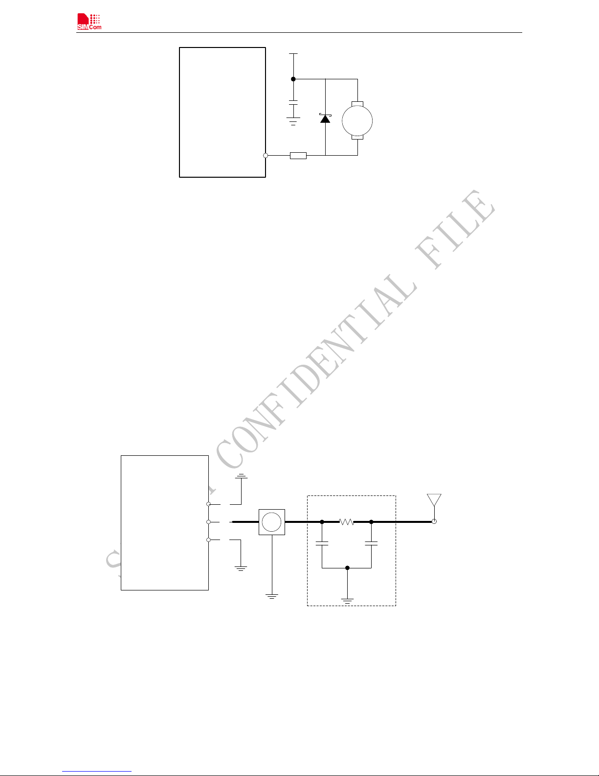
Vibrator
SIM8905A supports silent incoming-call alarms with its vibration motor driver. The vibration driver is a
programmable voltage output that is referenced to VBAT; when off, its output voltage is VBAT. The motor is
connected between VBAT and the VIB_DRV_N pin. The programmable motor voltage ranges from 1.2 to 3.1 V in
100 mV steps.
Page 25
Smart Machine Smart Decision
25
1uF
VBAT
VIB_DRV
Module
Vibrator
0R
Figure 25: Vibrator reference circuit
Antenna Interface
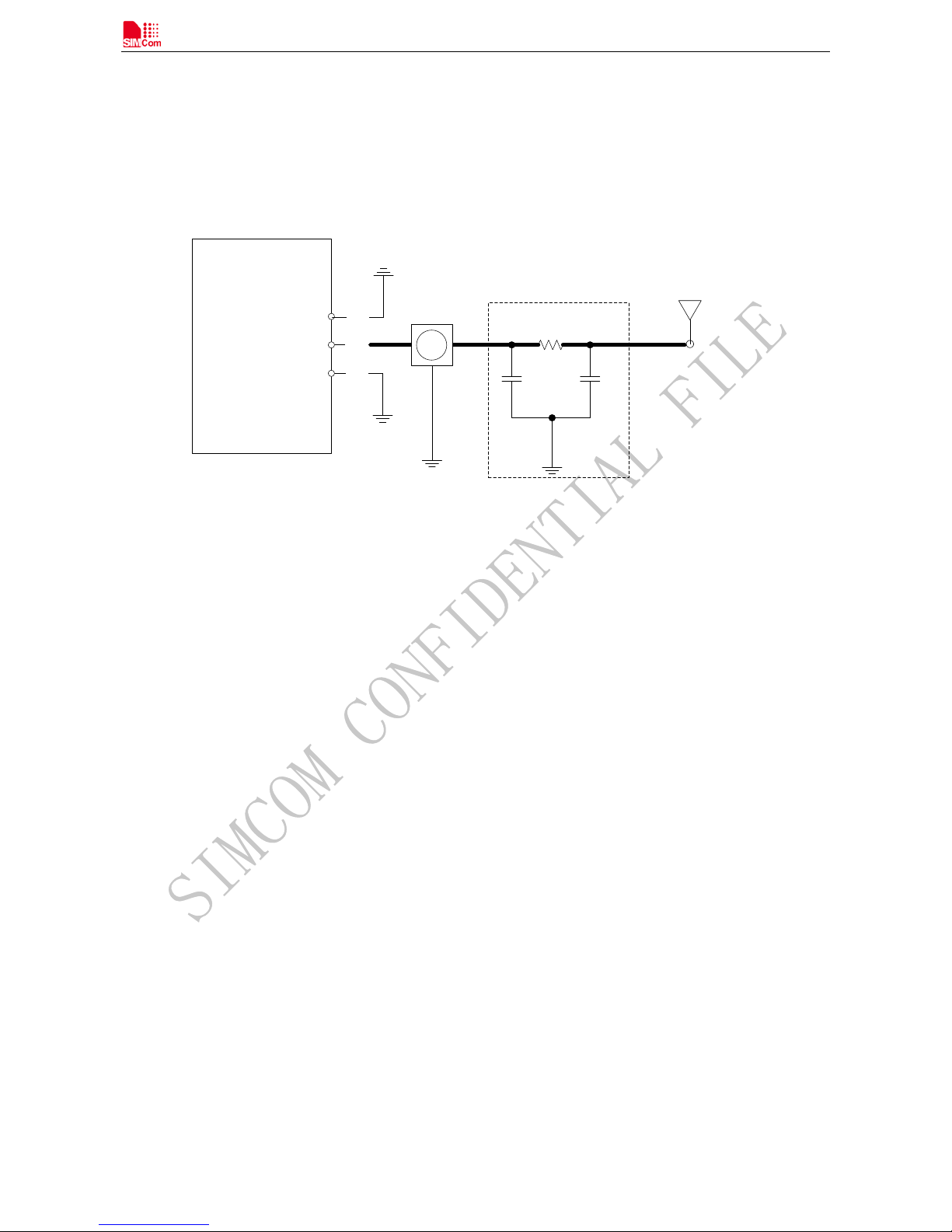
SIM8905A provides two antenna interfaces including MAIN antenna and DRX antenna. To ensure good RF
performance, users should meet the following requirements:
● Keep the RF traces at 50Ω.
● Maintain a complete and continuous reference ground plane from antenna pin to the RF connector.
● The RF traces should be away from any other noisy traces.
● Keep the RF traces as short as possible.
MAIN Antenna reference circuit
The recommended circuit is shown as below:
RF connector
(optional)
C1
Module
87
ANT_MAIN
GND
C2
88
R1
Matching circuit
MAIN ANT
86
GND
Figure 26: MAIN antenna recommended circuit
R1, C1 and C2 are antenna matching components in Figure 27, the value of these components are determined
according to the antenna tuning results. By default, R1 is 0Ω, C1 and C2 are reserved. The RF connector in Figure
27 is used to ensure the accuracy and convenience of the conduction testing, so SIMCOM suggest keeping it. If
considering Low-Cost BOM, user can cancel the connector.
Page 26
Smart Machine Smart Decision
26
DRX Antenna reference circuit
The recommended circuit is shown as below:
RF connector
(optional)
C1
Module
131
ANT_DRX
GND
C2
132
R1
Matching circuit
Diversity ANT
130
GND
Figure 27: DRX antenna recommended circuit
R1, C1 and C2 are antenna matching components in Figure 28, the value of these components are determined
according to the antenna tuning results. By default, R1 is 0Ω, C1 and C2 are reserved. The RF connector in Figure
28 is used to ensure the accuracy and convenience of the conduction testing, so SIMCOM suggest keeping it. If
considering Low-Cost BOM, user can cancel the connector.
Page 27

Smart Machine Smart Decision
27
PCB Layout
This section provides PCB layout guidelines for SIM8905A users to ensure their production against lots of issues,
and achieve the optimum performance.
Stack-up Options
At least, 4-layer through-hole PCB should be chosen for good impedance control and signal shielding.
General Placement Guidelines
Locate SIM8905A module in the center of PCB, rather than in the corner.
Digital devices and traces should not be placed near sensitive signals like RF and clock.
Keep SPKR and MIC away from sensitive RF lines.
PCB Layout Guideline Details
RF Trace
RF connector should be placed close to the module’s antenna pin.
Antenna matching circuit should be placed close to the antenna.
Keep the RF traces at 50Ω.
Maintain a complete and continuous reference ground plane from antenna pin to the RF connector.
The RF traces should be far away from any other noisy traces.
Keep the RF traces as short as possible.
If using a coaxial RF cable to connect the antenna, please avoid spanning on USIM cards, power circuits and
high-speed digital circuits to minimize the impact of each other.
Power/GND
Both VBAT and return path should be as short and wide as possible to minimize the IR drop
The VBAT current should go through Zener diode, capacitors, then VBAT pins
Must have a solid ground plane throughout the board as the primary reference plane for most signals
USIM Card
Ensure USIM card holder is far way from antenna or RF signal
Page 28
Smart Machine Smart Decision
28
ESD component and bypass c aps should be placed closed to USIM Card
USIM card signals should be far away from other high-speed signal
MIPI_DSI/CSI
Protect MIPI_DSI/CSI signals from noisy signals (clocks, SMPS, etc.)
Differential pairs, 100 Ω nominal, ±10%
Total routing length < 305 mm
Intra-pair length matching < 5 ps (0.67 mm)
Inter-pair length matching < 10 ps (1.3 mm)
Lane-to-lane trace spacing = 3x line width
Spacing to all other signals = 4x line width
Maintain a solid ground reference for clocks to provide a low-impedance path for return currents
Each trace needs to be next to a ground plane
Minimize the number of via on the trace
Refer to the following table for the length of MIPI traces inside the module.
Table 16: Length of MIPI traces inside the module
Pin#
Net Name
Length(mm)
52
MIPI_DSI_CLK_M
8.08
53
MIPI_DSI_CLK_P
9.03
54
MIPI_DSI_LANE0M
9.04
55
MIPI_DSI_LANE0P
8.73
56
MIPI_DSI_LANE1M
9.29
57
MIPI_DSI_LANE1P
9.10
58
MIPI_DSI_LANE2M
8.69
59
MIPI_DSI_LANE2P
8.95
60
MIPI_DSI_LANE3M
9.10
61
MIPI_DSI_LANE3P
9.85
63
MIPI_CSI0_CLK_M
14.04
64
MIPI_CSI0_CLK_P
13.79
65
MIPI_CSI0_LN0_M
13.27
66
MIPI_CSI0_LN0_P
13.23
67
MIPI_CSI0_LN1_M
13.96
68
MIPI_CSI0_LN1_P
14.49
70
MIPI_CSI1_CLK_M
17.21
71
MIPI_CSI1_CLK_P
17.69
72
MIPI_CSI1_LN0_M
16.34
73
MIPI_CSI1_LN0_P
17.25
USB
90 Ω differential, ± 10% trace impedance
Differential data pair matching < 6.6 mm (50 ps)
Page 29
Smart Machine Smart Decision
29
External components should be located near the USB connector.
Should be routed away from sensitive circuits and signals.
If there are test points, place them on the trace to keep branches as short as possible
If USB connector is used as the charger input, USB_VBUS node must be routed to the module using
extremely wide traces or sub planes.
Refer to the following table for the length of USB traces inside the module.
Table 17: Length of USB traces inside the module
Pin#
Net Name
Length(mm)
13
USB_DM
30.58
14
USB_DP
30.22
SDC Signal
Protect other sensitive signals/circuits from SDC corruption.
Protect SDC signals from noisy signals (clocks, SMPS, etc.).
Up to 200 MHz clock rate
50 Ω nominal, ±10% trace impedance
CLK to DATA/CMD length matching < 1 mm
30–35 Ω termination resistor on clock lines near the module
Total routing length < 50 mm recommended
Spacing to all other signals = 2x line width
Bus capacitance < 15 pF
Refer to the following table for the length of SD traces inside the module.
Table 18: Length of SD traces inside the module
Pin#
Net Name
Length(mm)
39
SD_CLK
14.24
40
SD_CMD
15.19
41
SD_DATA0
14.87
42
SD_DATA1
13.63
43
SD_DATA2
12.90
44
SD_DATA3
13.05
Audio
Analog input
4 to 5 mil trace widths; 4 to 5 mil spacing between traces
Differential route for MIC1P with GND_MIC and MIC2P with GND_MIC;
Isolate from noise sources, such as antenna, RF signals, SMPS, clocks, and other digital signals with fast
Page 30

Smart Machine Smart Decision
30
transients
Analog output
Coplanar ground fill on both sides (of traces or pair as appropriate); in between ground planes – grounds
above and below
Isolate from noise sources such as antenna, RF signals, SMPS, clocks, and other digital signals with fast
transients.
EAR output signal – route as differential pair with 10 mil trace widths.
SPK output signals – route as differential pair with 20 mil trace widths with 8 Ω load and 25 mil trace widths
with 4 Ω load
HPH output signals – not a differential pair; 10 mil trace widths for HPH_L and HPH_R; 15 mil trace widths
for HPH_GND
Connect HPH_GND to the ground pin of the jack connector and route HPH_GND in between HPH_L and
HPH_R for best crosstalk minimization
Page 31
SIM8905E Document
- 31 -
Electrical and Reliability
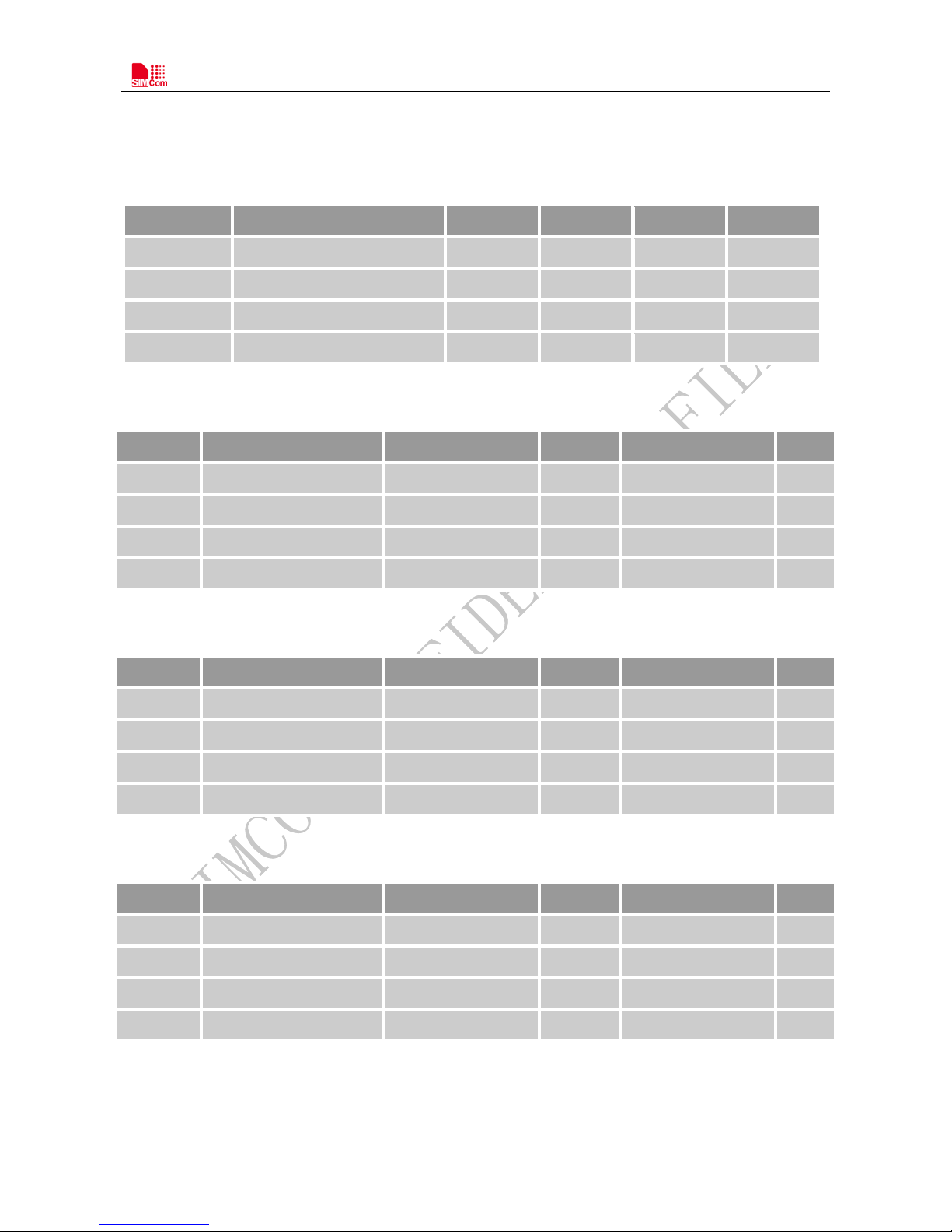
Absolute Maximum Ratings
Absolute maximum ratings reflect the stress levels that, if exceeded, may cause permanent damage to the device.
Functionality and reliability are only guaranteed within the operating conditions.
Table 19: Absolute maximum ratings
Parameter Min Max Unit
VBAT -0.3 5 V
VBUS -0.3 7 V
VRTC - 3.5 V
Temperature Range
Table 20: Temperature range
Parameter Min Typ Max Unit
Operating temperature -25 +75
℃
Storage temperature -40 +90
℃
Operating Voltage
Table 21: Operating voltage
Parameter Min Typ Max Unit
VBAT 3.4
3.9
4.4 V
VBUS 4.35
5
5.5 V
VRTC
2.0
3.0
3.25
V
Page 32
Smart Machine Smart D ecision
- 32 -
Digital-logic Characteristics
Table 22: 1.8 V digital I/O characteristics
Parameter Description Min Typ Max Unit
VIH
High-level input voltage 1.17 - - V
VIL
Low-level input voltage - - 0.63 V
VOH
High-level output voltage 1.35 - - V
VOL
Low-level output voltage - - 0.45 V
Table 23: USIM interface characteristics (USIM_VDD=1.8V/2.95V)
Parameter Description Min Typ Max Unit
VIH
High-level input voltage 0.7* USIM_VDD
-
USIM_VDD+0.3 V
VIL
Low-level input voltage
-0.3
-
0.2* USIM_VDD V
VOH
High-level output voltage 0.8*USIM_VDD
-
USIM_VDD V
VOL
Low-level output voltage 0
-
0.4 V
Table 24: SD interface characteristics (SD_LDO11 =1.8V)
Parameter Description Min Typ Max Unit
VIH
High-level input voltage 1.27
-
2 V
VIL
Low-level input voltage -0.3
-
0.58 V
VOH
High-level output voltage 1.4
-
- V
VOL
Low-level output voltage
0
-
0.45 V
Table 25: SD interface characteristics (SD_LDO11 =2.95V)
Parameter Description Min Typ Max Unit
VIH
High-level input voltage 0.625* SD_LDO11
-
SD_LDO11+0.3 V
VIL
Low-level input voltage
-0.3
-
0.25* SD_LDO11 V
VOH
High-level output voltage 0.75* SD_LDO11
-
SD_LDO11 V
VOL
Low-level output voltage 0
-
0.125* SD_LDO11 V
Page 33
Smart Machine Smart D ecision
- 33 -
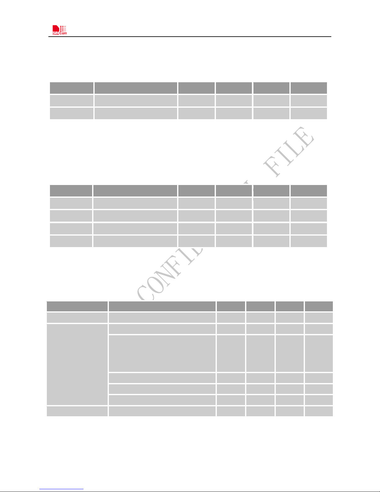
PWRKEY Characteristics
Table 26: PWRKEY characteristics
Parameters Description Min Typ Max Unit
VIH
High-level input voltage 1.4 - - V
VIL
Low-level input voltage - - 0.6 V
VRTC Characteristics
Table 27: VRTC characteristic
Parameter Description Min Typ Max Unit
VRTC
-IN
VRTC input voltage 2.0
3.0
3.25 V
I
RTC-IN
VRTC current consumption -
5
10 uA
VRTC
-OUT
VRTC output voltage
2.5
3.1
3.2
V
I
RTC-OUT
VRTC output current -
2 mA
Current Consumption (VBAT=3.9V)
Table 28: Current consumption
Parameter Conditions Min Typ Max Unit
Leakage current Off mode 20 uA
Standby current
Flight mode 1.22 mA
GSM:
BS-PA-MFRMS=9
BS-PA-MFRMS=5
BS-PA-MFRMS=2
1.65
1.85
3.00
mA
mA
mA
WCDMA, DRX=8 2.48 mA
LTE-FDD, standby 1.28s 2.11 mA
LTE-TDD, standby 1.28s 2.56 mA
Peak current 3.0 A
Electro-Static Discharge
Electrostatic discharge (ESD) occurs naturally in laboratory and factory environments. An established
Page 34
Smart Machine Smart D ecision
- 34 -
high-voltage potential is always at risk of disc harging to a lower potential. If this dis charge path is through a
semiconductor device, it may result in destructive damage.
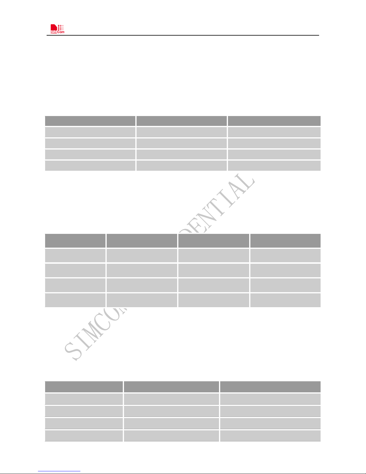
SIM8905A must be handled according to the ESD Association standard: ANSI/ESD S20.20-1999, Protection of
Electrical and Electronic Parts, Assemblies, and Equipment.
Table 29: ESD performance parameters(Temperature: 25℃, Humidity: 45%)
Pin
Contact discharge
Air discharge
VBAT
±5KV ±10 KV
GND
±5KV ±12KV
Antenna
±5KV ±10KV
PWRKEY
±4KV ±6KV
Module Operating Frequencies
Table 30: Module operating frequencies
Frequency Receive Transmit Physical channel
LTE B2 1930-1990 MHz 1850-1910 MHz
TX: 18600-19199
RX: 600-1199
LTE B4 2110-2155 MHz 1710-1755 MHz
TX: 19950-20399
RX: 1950-2399
LTE B5 869-894 MHz 824-849MHz
TX: 20400-20649
RX: 2400-2649
LTE B12 729-746MHz 699-716MHz
TX: 23010-23179
RX: 5010-5179
Module Output power
Table 31: Conducted transmission power
Frequency Power Min.
LTE-FDD B2 23dBm +/-2.7dB <-40dBm
LTE-FDD B4 23dBm +/-2.7dB <-40dBm
LTE-FDD B5 23dBm +/-2.7dB <-40dBm
LTE-FDD B12 23dBm +/-2.7dB <-40dBm
Page 35
Smart Machine Smart D ecision
- 35 -
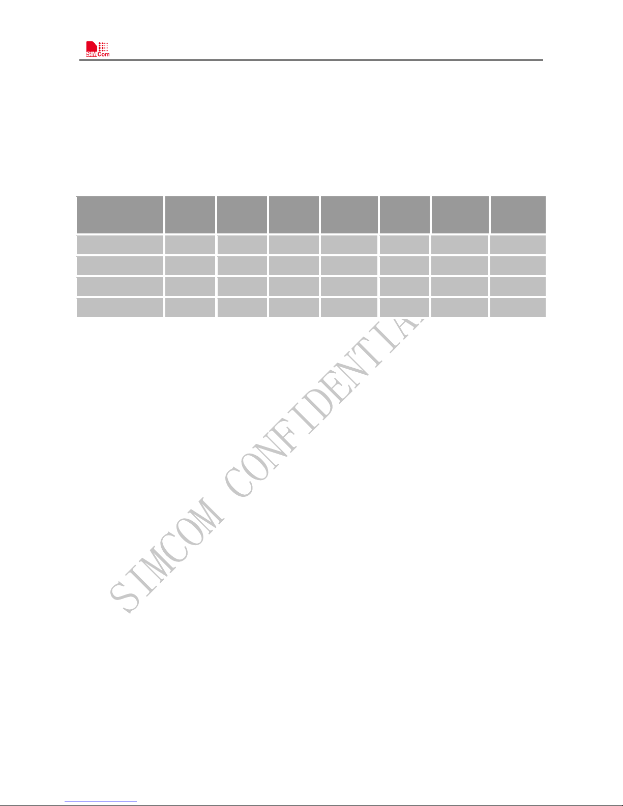
Module Receiving Sensitivity
Table 32: Reference sensitivity QPSk P
REFSENS
(LTE)
E-UTRA
Band number
1.4 MHz 3 MHz 5 MHz 10 MHz 15 MHz 20 MHz
Duplex
mode
2 -102.7 -99.7 -98 -95 -93.2 -92 FDD
4 -104.7 -101.7 -100 -97 -95.2 -94 FDD
5 -103.2 -100.2 -98 -95 FDD
12 -101.7 -98.7 -97 -94 FDD
Page 36

Smart Machine Smart D ecision
- 36 -
Contact us:
Shanghai SIMCom Wireless Solutions Co.,Ltd.
Address: Building B, SIM Technology Building, No. 633, Jinzhong Road, Shanghai, P. R. China
200335
Tel: + 86 21 3157 5100
Fax: +86 21 3157 5200
URL: http://simcomm2m.com/
 Loading...