

Page 1

SIM7600G-H,SIM7600G-H
SIMCom Wireless Solutions Limited
Building B, SIM Technology Building, No.633, Jinzhong Road
Changning District, Shanghai P.R. China
Tel: 86-21-31575100
support@simcom.com
www.simcom.com
LTE/HSPA/GSM/GNSS MODULE
miniPCIE
User manual
Page 2

SIM7600G-H User manual
Document Title:
SIM7600G-H User manual
Version:
V1.03
Date:
2020-05-09
Status:
Released
Document Control ID:
SIM7600G-H User manual
GENERAL NOTES
SIMCOM OFFERS THIS INFORMATION AS A SERVICE TO ITS CUSTOMERS, TO SUPPORT
APPLICATION AND ENGINEERING EFFORTS THAT USE THE PRODUCTS DESIGNED BY SIMCOM.
THE INFORMATION PROVIDED IS BASED UPON REQUIREMENTS SPECIFICALLY PROVIDED TO
SIMCOM BY THE CUSTOMERS. SIMCOM HAS NOT UNDERTAKEN ANY INDEPENDENT SEARCH
FOR ADDITIONAL RELEVANT INFORMATION, INCLUDING ANY INFORMATION THAT MAY BE IN THE
CUSTOMER’S POSSESSION. FURTHERMORE, SYSTEM VALIDATION OF THIS PRODUCT
DESIGNED BY SIMCOM WITHIN A LARGER ELECTRONIC SYSTEM REMAINS THE RESPONSIBILITY
OF THE CUSTOMER OR THE CUSTOMER’S SYSTEM INTEGRATOR. ALL SPECIFICATIONS
SUPPLIED HEREIN ARE SUBJECT TO CHANGE.
IC Caution:
This device complies with Industry Canada licence-exempt RSS standard(s). Operation is subject to the
following two conditions:
This device may not cause interference, and
(1)
This device must accept any interference, including interference that may cause undesired operation of
(2)
the device.
Le présent appareil est conforme aux CNR d'Industrie Canada applicables aux appareils radio exempts
de licence. L'exploitation est autorisée aux deux conditions suivantes:
l'appareil ne doit pas produire de brouillage, et
(1)
(2) l'utilisateur de l'appareil doit accepter tout brouillage radioélectrique subi, même si le brouillage est
susceptible d'en compromettre le fonctionnement
This equipment complies with ISED radiation exposure limits set forth for an uncontrolled environment.
This equipment should be installed and operated with minimum distance 20cm between the radiator &
your body.
Ce matériel est complété par une exposition de rayonnements IC pour un environnement naturel. Ce
matériel doit être installé et se faire avec une distance minimale de 20cm entre les radiateurs et les
autresYour body shop.
www.simcom.com
2/75
Page 3

SIM7600G-H User manual
For a host manufacture’s using a certified modular, if (1) the module’s IC number is not visible when
installed in the host, or (2) if the host is marketed so that end users do not have straightforward
commonly used methods for access to remove the module so that the IC number of the module is
visible; then an additional permanent label referring to the enclosed module: “Contains Transmitter
Module IC: 23761-8PYA008” or “Contains IC: 23761-8PYA008” must be used.
This radio transmitter IC: 23761-8PYA008 has been approved by Imovation,Science and Economic
Development Canada to operate with the antenna types listed below,with the maximm permissible gain
indicated.Antenna types not included in this list that have gain greater than the maximm gain indicated for
any type listed are strictly prohibilted for use with this device.
Antenna List:
Type: Dipole antenna with non-standard SMA connector(50ohm);
Model: MF25D
Antenna Gain:
Band 2:1.87dBi, Band 4:3.12dBi, Band 5:0.91dBi, Band 12:0.95dBi,
Band13:2.23dBi, Band 25:1.87dBi, Band 26:0.91dBi, Band 41:2.9dBi,
Band 66:3.12dBi
Single Module
Declaration of Conformity
SIMCom Wireless Solutions Limited, hereby declares that this LTE /HSPA/GSM/GNSS MODULE in
compliance with the essential requirements and other relevant provisions of Directive 2014/53/EU.
In accordance with Article 10(2) and Article 10(10),This product is allowed to be used in all EU member
states.
FCC Statement
This device complies with part 15 of the FCC Rules. Operation is subject to the following two
conditions:
(1) This device may not cause harmful interference, and
(2) this device must accept
any interference received, including interference that may cause undesired operation.
Any Changes or modifications not expressly approved by the party responsible for compliance
could void the user's authority to operate the equipment.
The modular can be installed or integrated in mobile or fix devices only. This modular cannot be
installed in any portable device.
FCC Radiation Exposure Statement
This modular complies with FCC RF radiation exposure limits set forth for an uncontrolled
www.simcom.com
3/75
Page 4

SIM7600G-H User manual
environment. This transmitter must not be co-located or operating in conjunction with any other
antenna or transmitter. This modular must be installed and operated with a minimum distance of 20 cm
between the radiator and user body.
If the FCC identification number is not visible when the module is installed inside another device,
then the outside of the device into which the module is installed must also display a label
referring to the enclosed module. This exterior label can use wording such as the following:
“Contains Transmitter Module FCC ID: 2AJYU-8PYA007 Or Contains FCC ID: 2AJYU-8PYA007”
When the module is installed inside another device, the user manual of the host must contain
below warning statements;
1. This device complies with Part 15 of the FCC Rules. Operation is subject to the following two
conditions:
(1) This device may not cause harmful interference.
(2) This device must accept any interference received, including interference that may cause
undesired operation.
2. Changes or modifications not expressly approved by the party responsible for compliance
could void the user's authority to operate the equipment.
The devices must be installed and used in strict accordance with the manufacturer's instructions
as described in the user documentation that comes with the product.
Any company of the host device which install this modular with Single modular approval should
perform the test of radiated emissionand spurious emission according to FCC part 15C : 15.247
and 15.209 requirement,Only if the test result comply with FCC part 15C : 15.247 and 15.209
requirement,then the host can be sold legally.
COPYRIGHT
THIS DOCUMENT CONTAINS PROPRIETARY TECHNICAL INFORMATION WHICH IS THE PROPERTY
OF SIMCOM WIRELESS SOLUTIONS LIMITED COPYING, TO OTHERS AND USING THIS DOCUMENT,
ARE FORBIDDEN WITHOUT EXPRESS AUTHORITY BY SIMCOM. OFFENDERS ARE LIABLE TO THE
PAYMENT OF INDEMNIFICATIONS. ALL RIGHTS RESERVED BY SIMCOM IN THE PROPRIETARY
TECHNICAL INFORMATION ,INCLUDING BUT NOT LIMITED TO REGISTRATION GRANTING OF A
PATENT , A UTILITY MODEL OR DESIGN. ALL SPECIFICATION SUPPLIED HEREIN ARE SUBJECT TO
CHANGE WITHOUT NOTICE AT ANY TIME.
manufacturer information:
SIMCom Wireless Solutions Limited
No.633, Jinzhong Rd,Changning Dist., Shanghai, P.R.China
Tel: +86 21 31575100
Email: simcom@simcom.com
www.simcom.com
4/75
Page 5

SIM7600G-H User manual
For more information, please visit:
https://www.simcom.com/download/list-863-en.html
For technical support, or to report documentation errors, please visit:
https://www.simcom.com/ask/ or email to: support@simcom.com
importer information:
importer Name:XXXX
importer Address:XXXX
Copyright © 2020 SIMCom Wireless Solutions Limited All Rights Reserved.
www.simcom.com
5/75
Page 6

Version History
Date
Version
Description of change
Author
2019-3-29
1.00
Original
Xutao.Jiang
2019-10-21
1.01
Update current consumption
Xutao.Jiang
2020-04-22
1.02
Modify the Format
Xiong Yuqing
2020-05-09
1.03
Add Sim7600NA/NA-H frequency band
Change Table 2
Xutao.Jiang
Qiang.Zhang
SIM7600G-H User manual
www.simcom.com
6/75
Page 7

Contents
SIM7600G-H User manual
Version History
Contents
................................................................................................................................................................
Table Index
Figure Index
1 Introduction
1.1 Product Outline............................................................................................................................................... 13
1.2 Hardware Interface Overview.......................................................................................................................14
1.3 Functional Overview...................................................................................................................................... 15
2 Package Information
2.1 Pin Assignment Overview............................................................................................................................. 17
2.2 Pin Description................................................................................................................................................20
2.3 Mechanical Information................................................................................................................................. 24
2.4 Footprint Recommendation.......................................................................................................................... 25
3 Interface Application
3.1 Power Supply..................................................................................................................................................26
3.1.1 Power Supply Design Guide.............................................................................................................27
3.1.2 Recommended Power Supply Circuit..............................................................................................28
3.1.3 Voltage Monitor....................................................................................................................................29
3.2 Power on/Power off/Reset Function............................................................................................................30
3.2.1 Power on...............................................................................................................................................30
3.2.2 Power off...............................................................................................................................................31
3.2.3 Reset Function.................................................................................................................................... 33
3.3 UART Interface............................................................................................................................................... 34
3.3.1 UART Design Guide...........................................................................................................................34
3.3.2 RI and DTR Behavior......................................................................................................................... 36
3.4 USB Interface..................................................................................................................................................37
3.5 HSIC interface.................................................................................................................................................38
3.6 SGMII Interface...............................................................................................................................................39
3.6.1 Reference schematic with AR8033..................................................................................................39
3.6.2 Reference schematic with BCM89820............................................................................................ 40
3.7 USIM Interface................................................................................................................................................40
3.7.1 USIM Application Guide..................................................................................................................... 41
3.8 PCM Interface................................................................................................................................................. 43
3.8.1 PCM timing...........................................................................................................................................43
3.8.2 PCM Application Guide...................................................................................................................... 45
3.9 SD Interface.....................................................................................................................................................45
3.10 I2C Interface..................................................................................................................................................47
3.11 SDIO Interface.............................................................................................................................................. 48
....................................................................................................................................................
............................................................................................................................................................
........................................................................................................................................................
.....................................................................................................................................................
.....................................................................................................................................
..................................................................................................................................
6
7
9
11
13
17
26
www.simcom.com
7/75
Page 8

SIM7600G-H User manual
3.12 SPI Interface................................................................................................................................................. 48
3.13 Network status..............................................................................................................................................49
3.14 Flight Mode Control......................................................................................................................................50
3.15 Other interface..............................................................................................................................................51
3.15.1 Sink Current Source.........................................................................................................................51
3.15.2 ADC..................................................................................................................................................... 52
3.15.3 LDO.....................................................................................................................................................52
4 RF Specifications
4.1. GSM/UMTS/LTE RF Specifications........................................................................................................... 53
4.2. LTE Antenna Design Guide......................................................................................................................... 54
4.3. GNSS.............................................................................................................................................................. 56
4.3.1 GNSS Technical specification...........................................................................................................56
4.3.2 GNSS Application Guide....................................................................................................................57
5 Electrical Specification
5.1 Absolute maximum ratings............................................................................................................................59
5.2 Operating conditions......................................................................................................................................59
5.3 Operating Mode..............................................................................................................................................60
5.3.1. Operating Mode Definition................................................................................................................60
5.3.2. Sleep mode.........................................................................................................................................61
5.3.3. Minimum functionality mode and Flight mode.............................................................................. 62
5.4 Current Consumption.....................................................................................................................................62
5.5 ESD Notes.......................................................................................................................................................63
6 SMT Production Guide
6.1 Top and Bottom View of MODULE.............................................................................................................. 64
6.2 Label Information............................................................................................................................................65
6.3 Typical SMT Reflow Profile...........................................................................................................................65
6.4 Moisture Sensitivity Level (MSL)................................................................................................................. 66
6.5 Stencil Foil Design Recommendation.........................................................................................................67
........................................................................................................................................
.............................................................................................................................
..............................................................................................................................
53
59
64
7 Packaging
8 Appendix
8.1 Coding Schemes and Maximum Net Data Rates over Air Interface..................................................... 71
8.2 Related Documents........................................................................................................................................71
8.3 Terms and Abbreviations...............................................................................................................................73
8.4 Safety Caution.................................................................................................................................................75
www.simcom.com
.....................................................................................................................................................
.......................................................................................................................................................
68
71
8/75
Page 9

SIM7600G-H User manual
Table Index
TABLE1 : MODULE FREQUENCY BANDS.............................................................................................................13
TABLE2 : GENERAL FEATURES.............................................................................................................................. 15
TABLE3 : PIN DEFINITION.........................................................................................................................................18
TABLE 4 : IO PARAMETERS DEFINITION..............................................................................................................20
TABLE 5 : PIN DESCRIPTION...................................................................................................................................20
TABLE 6 : VBAT PINS ELECTRONIC CHARACTERISTIC.................................................................................. 26
TABLE 7 : RECOMMENDED TVS LIST....................................................................................................................28
TABLE 8 : POWER ON TIMING AND ELECTRONIC CHARACTERISTIC........................................................31
TABLE 9 : POWER OFF TIMING AND ELECTRONIC CHARACTERISTIC......................................................32
TABLE 10 : RESET PIN ELECTRONIC CHARACTERISTIC............................................................................... 33
TABLE 11 : KEY DIFFERENCES BETWEEN HSIC AND HS-USB.....................................................................38
TABLE 12 : USIM ELECTRONIC CHARACTERISTIC IN 1.8V MODE (USIM_VDD=1.8V)........................... 40
TABLE 13 : USIM ELECTRONIC CHARACTERISTIC 3.0V MODE (USIM_VDD=2.95V).............................. 41
TABLE 14 : AMPHENOL USIM SOCKET PIN DESCRIPTION.............................................................................43
TABLE 15 : PCM FORMAT..........................................................................................................................................43
TABLE 16 : PCM TIMING PARAMETERS................................................................................................................44
TABLE 17 : SD/MMC ELECTRONIC CHARACTERISTIC AS 2.85V (SD_DATA0-3,SD_CLK AND SD_CMD)
..................................................................................................................................................................................45
TABLE 18 : SD/MMC/EMMC ELECTRONIC CHARACTERISTIC AS 1.8V (SD_DATA0-3,SD_CLK AND
SD_CMD) ............................................................................................................................................................. 46
TABLE 19 : NETLIGHT PIN STATUS........................................................................................................................ 49
TABLE 20 : FLIGHTMODE PIN STATUS..................................................................................................................50
TABLE 21 : SINK CURRENT ELECTRONIC CHARACTERISTIC...................................................................... 51
TABLE 22 : ADC1 AND ADC2 ELECTRONIC CHARACTERISTICS..................................................................52
TABLE 23 : ELECTRONIC CHARACTERISTIC......................................................................................................52
TABLE 24 : CONDUCTED TRANSMISSION POWER.......................................................................................... 53
TABLE 25 : OPERATING FREQUENCIES...............................................................................................................53
TABLE 26 : E-UTRA OPERATING BANDS..............................................................................................................53
TABLE 27 : CONDUCTED RECEIVE SENSITIVITY..............................................................................................54
TABLE 28 : REFERENCE SENSITIVITY (QPSK)...................................................................................................54
TABLE 29 : TRACE LOSS...........................................................................................................................................54
TABLE 30 : RECOMMENDED TVS...........................................................................................................................56
TABLE 31 : ABSOLUTE MAXIMUM RATINGS........................................................................................................59
TABLE 32 : RECOMMENDED OPERATING RATINGS........................................................................................ 59
TABLE 33 : 1.8V DIGITAL I/O CHARACTERISTICS*............................................................................................ 59
TABLE 34 : OPERATING TEMPERATURE..............................................................................................................60
TABLE 35 : OPERATING MODE DEFINITION........................................................................................................61
TABLE 36 : CURRENT CONSUMPTION ON VBAT PINS (VBAT=3.8V)............................................................62
TABLE 37 : THE ESD PERFORMANCE MEASUREMENT TABLE (TEMPERATURE: 25℃, HUMIDITY:
45%)........................................................................................................................................................................ 63
TABLE 38 : THE DESCRIPTION OF LABEL INFORMATION.............................................................................. 65
www.simcom.com
9/75
Page 10

SIM7600G-H User manual
TABLE 39 : MOISTURE SENSITIVITY LEVEL AND FLOOR LIFE..................................................................... 66
TABLE 40 : TRAY SIZE................................................................................................................................................68
TABLE 41 : SMALL CARTON SIZE........................................................................................................................... 69
TABLE 42 : BIG CARTON SIZE................................................................................................................................. 70
TABLE 43 : CODING SCHEMES AND MAXIMUM NET DATA RATES OVER AIR INTERFACE.................. 71
TABLE 44 : RELATED DOCUMENTS.......................................................................................................................71
TABLE 45 : TERMS AND ABBREVIATIONS............................................................................................................73
TABLE 46 : SAFETY CAUTION................................................................................................................................. 75
www.simcom.com
10/75
Page 11

SIM7600G-H User manual
Figure Index
FIGURE 2 : PIN ASSIGNMENT OVERVIEW...........................................................................................................17
FIGURE 3 : DIMENSIONS (UNIT: MM).....................................................................................................................24
FIGURE 4 : FOOTPRINT RECOMMENDATION (UNIT: MM)...............................................................................25
FIGURE 5 : VBAT VOLTAGE DROP DURING BURST EMISSION (GSM/GPRS)...........................................26
FIGURE 6 : POWER SUPPLY APPLICATION CIRCUIT.......................................................................................27
FIGURE 7 : LINEAR REGULATOR REFERENCE CIRCUIT................................................................................28
FIGURE 8 : SWITCHING MODE POWER SUPPLY REFERENCE CIRCUIT...................................................29
FIGURE 9 : REFERENCE POWER ON/OFF CIRCUIT.........................................................................................30
FIGURE 10 : POWER ON TIMING SEQUENCE.................................................................................................... 31
FIGURE 11 : POWER OFF TIMING SEQUENCE...................................................................................................32
FIGURE 12 : REFERENCE RESET CIRCUIT.........................................................................................................33
FIGURE 13 : UART FULL MODEM........................................................................................................................... 34
FIGURE 14 : UART NULL MODEM...........................................................................................................................34
FIGURE 15 : REFERENCE CIRCUIT OF LEVEL SHIFT...................................................................................... 35
FIGURE 16 : LEVEL MATCHING CIRCUIT............................................................................................................. 35
FIGURE 17 : RI BEHAVIOUR(SMS AND URC REPORT)...............................................................................36
FIGURE 18 : RI BEHAVIOUR(VOICE CALL).................................................................................................. 36
FIGURE 19 : USB REFERENCE CIRCUIT..............................................................................................................37
FIGURE 20 : REFERENCE SGMII CIRCUIT WITH AR8033................................................................................39
FIGURE 21 : REFERENCE SGMII CIRCUIT WITH BCM89820..........................................................................40
FIGURE 22 : USIM INTERFACE REFERENCE CIRCUIT.................................................................................... 41
FIGURE 23 : USIM INTERFACE REFERENCE CIRCUIT WITH USIM_DET................................................... 42
FIGURE 24 : AMPHENOL SIM CARD SOCKET.....................................................................................................43
FIGURE 25 : PCM_SYNC TIMING............................................................................................................................44
FIGURE 26 : EXT CODEC TO MODULE TIMING..................................................................................................44
FIGURE 27 : MODULE TO EXT CODEC TIMING..................................................................................................44
FIGURE 28 : AUDIO CODEC REFERENCE CIRCUIT..........................................................................................45
FIGURE 29 : SD REFERENCE CIRCUIT................................................................................................................ 46
FIGURE 30 : EMMC REFERENCE CIRCUIT..........................................................................................................47
FIGURE 31 : I2C REFERENCE CIRCUIT................................................................................................................48
FIGURE 32 : NETLIGHT REFERENCE CIRCUIT.................................................................................................. 49
FIGURE 33 : FLIGHT MODE SWITCH REFERENCE CIRCUIT..........................................................................50
FIGURE 34 : ISINK REFERENCE CIRCUIT............................................................................................................51
FIGURE 35 : ANTENNA MATCHING CIRCUIT (MAIN_ANT)...............................................................................55
FIGURE 36 : ANTENNA MATCHING CIRCUIT (AUX_ANT).................................................................................55
FIGURE 37 : ACTIVE ANTENNA CIRCUIT..............................................................................................................57
FIGURE 38 : PASSIVE ANTENNA CIRCUIT (DEFAULT)..................................................................................... 57
FIGURE 39 : TOP AND BOTTOM VIEW OF MODULE.........................................................................................64
FIGURE 40 : LABEL INFORMATION........................................................................................................................ 65
FIGURE 41 : THE RAMP-SOAK-SPIKE REFLOW PROFILE OF MODULE.....................................................66
FIGURE 42 : STENCIL FOIL....................................................................................................................................68
www.simcom.com
11/75
Page 12

SIM7600G-H User manual
FIGURE 43 : PACKAGING DIAGRAM......................................................................................................................68
FIGURE 44 : TRAY DRAWING...................................................................................................................................68
FIGURE 45 : SMALL CARTON DRAWING.............................................................................................................. 69
FIGURE 46 : BIG CARTON DRAWING.................................................................................................................... 70
www.simcom.com
12/75
Page 13

SIM7600G-H User manual
Standard
Frequency
SIM7600G
SIM7600G-H
SIM7600NA
SIM7600NA-H
GSM
850MHz
900MHz
1800M Hz
1900M Hz
WCDMA
B1
B2
B4
B5
B6
B8
B19
LTE
FDD B1
FDD B2
√
√
√
√
FDD B3
FDD B4
√
√
√
√
FDD B5
√
√
√
√
FDD B7
FDD B8
FDD B12
√
√
√
√
FDD B13
√
√
√
√
1 Introduction
This document describes the electronic specifications, RF specifications, interfaces, mechanical
characteristics and testing results of the SIMCom module. With the help of this document and other
software application notes/user guides, users can understand and use module to design and develop
applications quickly.
1.1 Product Outline
Aimed at the global market, the module support GSM, WCDMA, LTE-TDD and LTE-FDD. Users can choose
the module according to the wireless network configuration. The supported radio frequency bands are
described in the following table.
Table1: Module frequency bands
www.simcom.com
13/75
Page 14

SIM7600G-H User manual
FDD B14
√
√
FDD B18
FDD B19
FDD B20
FDD B25
√
√
√
√
FDD B26
√
√
√
√
FDD B28
FDD B66
√
√
√
√
FDD B71
√
√
TDD B34
TDD B38
TDD B39
TDD B40
TDD B41
√
√
√
√
Category
CAT1
CAT4
CAT1
CAT4
With a small physical dimension of 30*30*2.9 mm and with the functions integrated, the module can meet
almost any space requirement in users’ applications, such as smart phone, PDA, industrial handhold,
machine-to-machine and vehicle application, etc.
1.2 Hardware Interface Overview
The interfaces are described in detail in the next chapters include:
● Power Supply
● USB2.0 Interface
● UART Interface
● MMC/SD Interface
● SDIO Interface
● USIM Interface
● SPI Interface
● GPIO
● ADC
● LDO Power Output
● Current Sink Source
● PCM Interface
● SPI Interface
● I2C Interface
● HSIC Interface
● SGMII Interface
www.simcom.com
14/75
Page 15
1.3 Functional Overview
Feature
Implementation
Power supply
Single supply voltage 3.4~4.2V, Recommend supply voltage 3.8V
Power saving
Current in sleep mode : <5mA
Radio frequency bands
Please refer to the table 1
Transmitting power
LTE power class: 3 (24+1/-2dBm)
Data Transmission
Throughput
LTE CAT 4 :150 Mbps (DL)
50 Mbps (UL)
Antenna
LTE main antenna.
LTE auxiliary antenna
GNSS antenna
GNSS
GNSS engine (GPS,GLONASS,BD,QZSS and GALILEO)
Protocol: NMEA 0183
SMS
MT, MO, CB, Text and PDU mode
SMS storage: USIM card or ME(default)
Transmission of SMS alternatively over CS or PS.
USIM interface
Support identity card: 1.8V/ 3V
USIM application toolkit
Support SAT class 3, GSM 11.14 Release 98
Support USAT
Phonebook management
Support phonebook types: DC,MC,RC,SM,ME,FD,ON,LD,EN
Audio feature
Support PCM interface
Only support PCM master mode and short frame sync, 16-bit linear data
formats
UART interface
A full modem serial port by default
Baud rate: 300bps to 4Mbps(default:115200bps)
Autobauding baud rate: 9600,19200,38400,57600,115200bps
Can be used as the AT commands or data stream channel
Support RTS/CTS hardware handshake
Multiplex ability according to GSM 07.10 Multiplexer Protocol
MMC/SD
Support MMC and SD cards with 2.85 V on SD port
SDIO
Support SDIO with 1.8 V only on SDIO port
USB
USB 2.0 high speed interface, Can used be send AT command, Software
update, GNSS NMEA,USB voice function etc.
Firmware upgrade
Firmware upgrade over USB interface or FOTA
Physical characteristics
Size:30*30*2.9m
Weight:5.7 g
Temperature range
Normal operation temperature: -30°C to +80°C
Extended operation temperature: -40°C to +85°C*
Storage temperature -45°C to +90°C
antenna type
Dipole(SMA connector)
Table2: General features
SIM7600G-H User manual
www.simcom.com
15/75
Page 16
SIM7600G-H User manual
max. output power
LTE Band 2: 23.20 dBm
LTE Band 4: 23.67 dBm
LTE Band 5: 25.30 dBm
LTE Band 12: 24.35 dBm
LTE Band 13: 22.06 dBm
LTE Band 25: 23.46 dBm
LTE Band 26: 24.16 dBm
LTE Band 41: 23.16 dBm
LTE Band 66: 23.08 dBm
frequency range
Tx:
LTE Band2:1850~1910MHz,LTE Band4:1710MHz~1755MHz
LTE Band5:824~849MHz,LTE Band12:699~716MHz
LTE Band13:777~787MHz,LTE Band25:1850~1915MHz
LTE Band26:814~849MHz,LTE Band41:2496MHz~2690MHz
LTE Band66:1710MHz~1780MHz
Rx:
LTE Band2:1930~1990MHz,LTE Band4:2110MHz~2155MHz
LTE Band5:869~894MHz,LTE Band12:729~746MHz
LTE Band13:746~756MHz,LTE Band25:1930~1995MHz
LTE Band26:859~894MHz,LTE Band41:2496MHz~2690MHz
LTE Band66:2110MHz~2200MHz
GPS: 1575.42MHz; BDS: 1559MHz~1563MHz
Module is able to make and receive voice calls, data calls, SMS and make LTE traffic in -40℃ ~ +85℃.
The performance will be reduced slightly from the 3GPP specifications if the temperature is outside the
normal operating temperature range and still within the extreme operating temperature range.
NOTE
www.simcom.com
16/75
Page 17
SIM7600G-H User manual
2 Package Information
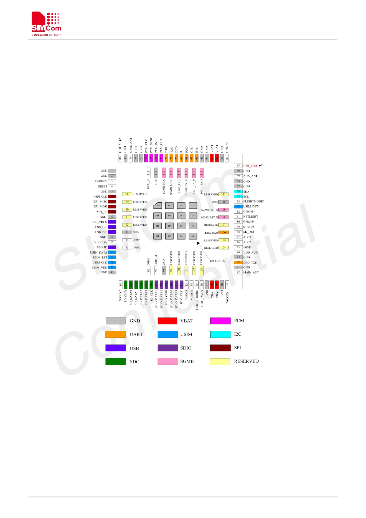
2.1 Pin Assignment Overview
All functions of the MODULE will be provided through 135 pads that will be connected to the users’ platform.
The following Figure is a high-level view of the pin assignment of the MODULE.
www.simcom.com
Figure 2: Pin assignment overview
17/75
Page 18
Table3: Pin definition
Pin No.
Pin name
Pin No.
Pin name
1
GND
2
GND
3
PWRKEY
4
RESET
5
GND
6
SPI_CLK*
7
SPI_MISO*
8
SPI_MOSI*
9
SPI_CS*
10
GND
11
USB_VBUS
12
USB_DN
13
USB_DP
14
GND
15
VDD_1V8
16
USB_ID
17
USIM_DATA
18
USIM_RST
19
USIM_CLK
20
USIM_VDD
21
SD_CMD
22
SD_DATA0
23
SD_DATA1
24
SD_DATA2
25
SD_DATA3
26
SD_CLK
27
SDIO_DATA1
28
SDIO_DATA2
29
SDIO_CMD
30
SDIO_DATA0
31
SDIO_DATA3
32
SDIO_CLK
33
GPIO3*
34
GPIO6*
35
HSIC_STROBE
36
HSIC_DATA
37
GND
38
VBAT
39
VBAT
40
GND
41
GND
42
DBG_TXD
43
GND
44
VDD_AUX
45
ISINK
46
ADC2
47
ADC1
48
SD_DET
49
STATUS
50
GPIO43*
51
NETLIGHT
52
GPIO41*
53
USIM_DET*
54
FLIGHTMODE*
55
SCL
56
SDA
57
GND
58
GND
59
AUX_ANT
60
GND
61
GND
62
VBAT
63
VBAT
64
GND
65
GND
66
RTS
67
CTS
68
RXD
69RI70
DCD
71
TXD
72
DTR
73
PCM_OUT
74
PCM_IN
75
PCM_SYNC
76
PCM_CLK
SIM7600G-H User manual
www.simcom.com
18/75
Page 19

SIM7600G-H User manual
77
GND
78
GND
79
GNSS_ANT
80
GND
81
GND
82
MAIN_ANT
83
COEX1●*
84
COEX2*
85
BOOT_CFG0●*
86
COEX3●*
87
GPIO77
88
RESERVED
89
RESERVED
90
RESERVED
91
RESERVED
92
RESERVED
93
GND
94
GPIO4
95
GPIO2
96
GPIO1
97
GPIO_54
98
GND
99
RESERVED
100
RESERVED
101
RESERVED
102
RESERVED
103
RESERVED
104
RESERVED
105
RESERVED
106
DBG_ RXD
107
RESERVED
108
SGMII_RST_N
109
SGMII_INT_N
110
GND
111
RESERVED
112
SGMII_RX_P
113
SGMII_RX_M
114
SGMII_TX_M
115
SGMII_TX_P
116
SGMII_MDIO
117
SGMII_MDC
118
GND
119
GPIO_19
120
GND
121
GND
122
GND
123
GND
124
GND
125
GND
126
GND
127
GND
128
GND
129
GND
130
GND
131
GND
132
GND
133
GND
134
GND
135
GND
● Means Before the normal power up, COEX1, COEX3 or BOOT_CFG0 cannot be pulled up,
otherwise module will not be powered up normally.
* Means that pins has MUX function.
NOTE
www.simcom.com
19/75
Page 20
2.2 Pin Description
Pin type
Description
PI
Power input
PO
Power output
AI
Analog input
AIO
Analog input/output
I/O
Bidirectional input /output
DI
Digital input
DO
Digital output
DOH
Digital output with high level
DOL
Digital output with low level
PU
Pull up
PD
Pull down
Pin name
Pin No.
Default
status
Description
Comment
Power supply
VBAT
38,39,
62,63
PI
Power supply, voltage range:
3.4~4.2V.
VDD_AUX
44
PO
LDO power output for other
external circuits with Max 150mA
current output. Its output voltage
is 2.85V by default.(The voltage
can be configured from 1.7V to
3.05V by AT command).
If used SGMII
function ,this pin
used for SGMII
function.
If unused, keep it
open.
VDD_1V8
15
PO
1.8 output with Max 50mA current
output for external circuit, such as
level shift circuit.
If unused, keep it
open.
GND
1,2,5,
10,14,37,
40,41,43,
57,58,60,
61,64,65,
77,78,80,
81,93,96,
110,118,1
20,121,1
22,123,1
24,125,1
26,127,1
28,129,1
30,131,1
32,133,1
Ground
Table 4: IO parameters definition
SIM7600G-H User manual
Table 5: Pin description
www.simcom.com
20/75
Page 21
SIM7600G-H User manual
34135
System Control
PWRKEY
3
DI,PU
System power on/off control input,
active low.
The high voltage is
0.8V;
RESET
4
DI, PU
System reset control input, active
low.
RESET has been
pulled up to 1.8V via
40Kohm resistor
internally.
SD interface
SD_CMD
21
I/O,PD
SDIO command
If unused, keep them
open.
SD_DATA0
22
I/O,PD
SDIO data
SD_DATA1
23
I/O,PD
SD_DATA2
24
I/O,PD
SD_DATA3
25
I/O,PD
SD_CLK
26DOSDIO clock
SD_DET
48
DI,PU
SD card insertion detect
H: SD card is removed
L: SD card is inserted
USIM interface
USIM_DATA
17
I/O,PU
USIM Card data I/O, which has
been pulled up via a 10KR
resistor to USIM_VDD internally.
Do not pull it up or down
externally.
All lines of USIM
interface should be
protected against
ESD.
USIM_RST
18
DO,PD
USIM Reset
USIM_CLK
19
DO,PD
USIM clock
USIM_VDD
20
PO,PD
Power output for USIM card, its
output Voltage depends on USIM
card type automatically. Its output
current is up to 50mA.
SPI interface
SPI_CLK*
6DOSPI clock output
Default SPI
Optional: BT uart
function
SPI_MISO*
7
DI
SPI master in/slave out data
SPI_MOSI*
8
DO
SPI master out/slave in data
SPI_CS*
9DOSPI chip-select output
USB
USB_VBUS
11
AI
Valid USB detection input with
3.0~5.25V detection voltage
USB_DN
12
AI, AO
Negative line of the differential,
bi-directional USB signal.
USB_DP
13
AI, AO
Positive line of the differential,
bi-directional USB signal.
USB_ID
16AIHigh-speed USB ID input
Keep it open.
SGMII interface
SGMII_RX_P
112AISGMII receive – positive
If unused, keep them
open.
SGMII_RX_M
113AISGMII receive - negative
SGMII_TX_M
114AOSGMII transmit - negative
www.simcom.com
21/75
Page 22

SIM7600G-H User manual
SGMII_TX_P
115AOSGMII transmit– positive
SGMII_RST_N
108DOEthernet PHY reset
External 1.5K pull-up
resistor from
3.3V/2.5V to
MDIO_DATA and
10K pull-up resistor
from VDD_1V8 to
ETH_INT_N are
needed when the
Ethernet PHY is
connected.
If unused, please
keep them open.
SGMII_INT_N
109
DI,PU
Ethernet PHY interrupt
SGMII_MDIO
116
DIO
Management data
input/output-data
SGMII_MDC
117
DO
Management data
input/output-clock
UART interface
RTS
66
DOH
Request to send
If unused, keep them
open.
CTS
67DIClear to Send
RXD
68DIReceive Data
RI69DOH
Ring Indicator
DCD
70
DOH
Carrier detects
TXD
71
DOH
Transmit Data
DTR
72
DI,PU
DTE get ready
DBG_UART
DBG_TXD
42DOLog output
If unused, keep them
open.
DBG_RXD
106DILog input
I2C interface
SCL
55ODI2C clock output
If unused, keep
open, or else pull
them up via 2.2KΩ
resistors to 1.8V.
SDA
56ODI2C data input/output
SDIO interface
SDIO_DATA1
27
I/O
SDIO data1
It can be used for
WLAN function.
If unused, please
keep them open.
SDIO_DATA2
28
I/O
SDIO data2
SDIO_CMD
29
I/O
SDIO command
SDIO_DATA0
30
I/O
SDIO data0
SDIO_DATA3
31
I/O
SDIO data3
SDIO_CLK
32
DO
SDIO clock
HSIC interface
HSIC_STROBE
35
I/O
HSIC strobe wakeup
If use, please refer
to document [27]
Otherwise please
keep them open.
HSIC_DATA
36
I/O
HSIC data
PCM interface
PCM_OUT
73
DO,PD
PCM data output.
If unused, please
keep them open.
PCM_IN
74
DI,PD
PCM data input.
PCM_SYNC
75
I/O,PD
PCM data frame sync signal.
www.simcom.com
22/75
Page 23

SIM7600G-H User manual
PCM_CLK
76
I/O,PU
PCM data bit clock.
GPIO
NETLIGHT
51
DO,PU
LED control output as network
status indication.
If unused, keep them
open.
STATUS
49
DO,PU
Operating status output.
High level: Power on and firmware
ready
Low level: Power off
GPIO4
94
IO,PD
Default: GPIO
GPIO2
95
IO,PD
Default: GPIO
GPIO1
96
IO,PD
Default: GPIO
GPIO_54
97
IO,PD
Default: GPIO
GPIO_19
119
IO,PD
Default: GPIO
RF interface
MAIN _ANT
82
AIO
MAIN antenna soldering pad
GNSS_ANT
79AIGNSS antenna soldering pad
AUX_ANT
59AIAuxiliary antenna soldering pad
Other interface
ISINK
45PIGround-referenced current sink.
If unused, please
keep them open.
ADC1
47AIAnalog-digital converter input 1
ADC2
46AIAnalog-digital converter input 2
RESERVED
88,89,90,
91,92,99,
100,101,
102,103,
104,105,
107,111
Reserved for future use
Please keep them
open.
Mux function interface
COEX1●*
83
I/O
RF synchronizing between Wi-Fi
and LTE.
Default:COEX1●*
Option:WLAN_EN●
COEX2*
84
I/O
RFsynchronizing between Wi-Fi
and LTE.
Default:COEX2*
Option: WoWWAN●
COEX3●*
86
I/O
RF synchronizing between Wi-Fi
and LTE.
Default:COEX3*
Option:BT_PCM_CL
K●
BOOT_CFG0●*
85
DI,PD
Boot configuration input.
Module will be forced into USB
download mode by connect 85 pin
to VDD_1V8 during power up.
Default:
BOOT_CFG0●*
Option:COEX_RXD●
Do place 2 test
points for debug.
DO NOT PULL UP
BOOT_CFG0
DURING NORMAL
POWER UP!
FLIGHTMODE*
54
DI,PU
Flight Mode control input.
High level(or open): Normal Mode
Low level: Flight Mode
Default:
FLIGHTMODE*
Option:BT_PCM_IN●
GPIO3*
33IOGPIO
Default:GPIO3*
Option:WL_PWR_E
N●
www.simcom.com
23/75
Page 24

SIM7600G-H User manual
GPIO6*
34IOGPIO
Default:GPIO6*
Option:WL_SLP_CL
K●
USIM_DET*
53
IO
Default: GPIO
Optional: USIM card detecting
input.
H: USIM is removed
L: USIM is inserted
Default:USIM_DET*
Option:BT_EN●
GPIO77*
87IOGPIO
Default:GPIO77*
Option:BT_PCM_OU
T●
GPIO43*
50
I/O,PD
GPIO
Default:GPIO43*
Option:COEX_TXD●
GPIO41*
52
I/O,PD
GPIO
Default:GPIO41*
Option:BT_PCM_SY
NC●
2.3 Mechanical Information
The following figure shows the package outline drawing of MODULE.
www.simcom.com
Figure 3: Dimensions (Unit: mm)
24/75
Page 25

2.4 Footprint Recommendation
SIM7600G-H User manual
www.simcom.com
Figure 4: Footprint recommendation (Unit: mm)
25/75
Page 26
SIM7600G-H User manual
The test condition: The voltage of power supply for VBAT is 3.8V, Cd=100 µF tantalum capacitor
(ESR=0.7Ω) and Cf=100nF (Please refer to Figure 6—Application circuit).
Symbol
Description
Min.
Typ.
Max.
Unit
VBAT
Module power voltage
3.4
3.8
4.2
V
I
VBAT(peak)
Module power peak current in normal mode.
-2-
A
I
VBAT(average)
Module power average current in normal mode
Please refer to the table 34
I
VBAT(sleep)
Power supply current in sleep mode
I
VBAT(power-off)
Module power current in power off mode.
--20
uA
NOTE
3 Interface Application
3.1Power Supply
The power supply pins of MODULE include 4 pins (pin 62&63, pin 38&39) named VBAT.
The 4 VBAT pads supply the power to RF and baseband circuits directly. On VBAT pads, the ripple current
up to 2A typically, due to GSM/GPRS emission burst (every 4.615ms), may cause voltage drop. So the
power supply for these pads must be able to provide sufficient current up to more than 2A in order to avoid
the voltage drop is more than 300mV.
The following figure shows the VBAT voltage ripple wave at the maximum power transmit phase.
Figure 5: VBAT voltage drop during burst emission (GSM/GPRS)
Table 6: VBAT pins electronic characteristic
www.simcom.com
26/75
Page 27
SIM7600G-H User manual
If the power supply for VBAT pins can support up to 2A, more than 300uF capacitors are
recommended .Otherwise users must use a total of 1000uF capacitors typically, in order to avoid of the
voltage drop more than 300mV.
user could only power pin 62, 63 or only power pin 38, 39, for these pins are connected inside the
MODULE.
NOTE
NOTE
3.1.1 Power Supply Design Guide
Make sure that the voltage on the VBAT pins will never drop below 3.4V, even during a transmit burst, when
current consumption may rise up to 2A. If the voltage drops below 3.4V, the RF performance may be
affected.
Some multi-layer ceramic chip (MLCC) capacitors (0.1/1uF) with low ESR in high frequency band can be
used for EMC.
These capacitors should be put as close as possible to VBAT pads. Also, users should keep VBAT trace on
circuit board wider than 2 mm to minimize PCB trace impedance. The following figure shows the
recommended circuit.
Recommend Bead for vbat filter are BLM21PG300SN1D and MPZ2012S221A。
Figure 6: Power supply application circuit
In addition, in order to guard for over voltage protection, it is suggested to use TVS.
www.simcom.com
27/75
Page 28

Table 7: Recommended TVS list
No.
Manufacturer
Part Number
Power dissipation
Package
1
JCET
ESDBW5V0A1
5V
DFN1006-2L
2
WAYON
WS05DPF-B
5V
DFN1006-2L
3
WILLSEMI
ESD5611N
5V
DFN1006-2L
4
WILLSEMI
ESD56151W05
5V
SOD-323
5*
PRISEMI
PESDHC2FD4V5BH
4.5V
DFN1006-2L
6*
WAYON
WS4.5DPV
4.5V
DFN1610-2L
If user chooses TVS, please pay attention to Clamping Voltage in your datasheet . For example when
the surge input is 100V,the Clamping Voltage is less than 10V.
*If vbat is higher than 3.8V, do not choose NO. 5 and NO. 6.
NOTE
SIM7600G-H User manual
3.1.2 Recommended Power Supply Circuit
It is recommended that a switching mode power supply or a linear regulator power supply is used. It is
important to make sure that all the components used in the power supply circuit can resist a peak current up
to 2A.
The following figure shows the linear regulator reference circuit with 5V input and 3.8V output.
Figure 7: Linear regulator reference circuit
If there is a big voltage difference between input and output for VBAT power supply, or the efficiency is
www.simcom.com
28/75
Page 29
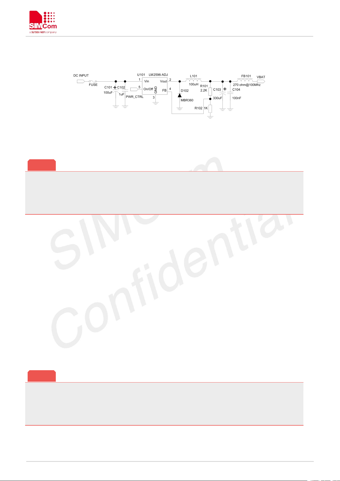
SIM7600G-H User manual
The Switching Mode power supply solution for VBAT must be chosen carefully against Electro Magnetic
Interference and ripple current from depraving RF performance.
Under-voltage warning function and under-voltage power-off function are disabled by default. For more
information about these AT commands, please refer to Document [1].
NOTE
NOTE
extremely important, then a switching mode power supply will be preferable. The following figure shows the
switching mode power supply reference circuit.
Figure 8: Switching mode power supply reference circuit
3.1.3 Voltage Monitor
To monitor the VBAT voltage, the AT command “AT+CBC” can be used.
For monitoring the VBAT voltage outside or within a special range, the AT command “AT+CVALARM” can
be used to enable the under-voltage warning function.
If users need to power off MODULE, when the VBAT voltage is out of a range, the AT command
“AT+CPMVT” can be used to enable under-voltage power-off function.
Note: Under-voltage warning function and under-voltage power-off function are disabled by default. For
more information about these AT commands, please refer to Document [1].
www.simcom.com
29/75
Page 30
SIM7600G-H User manual
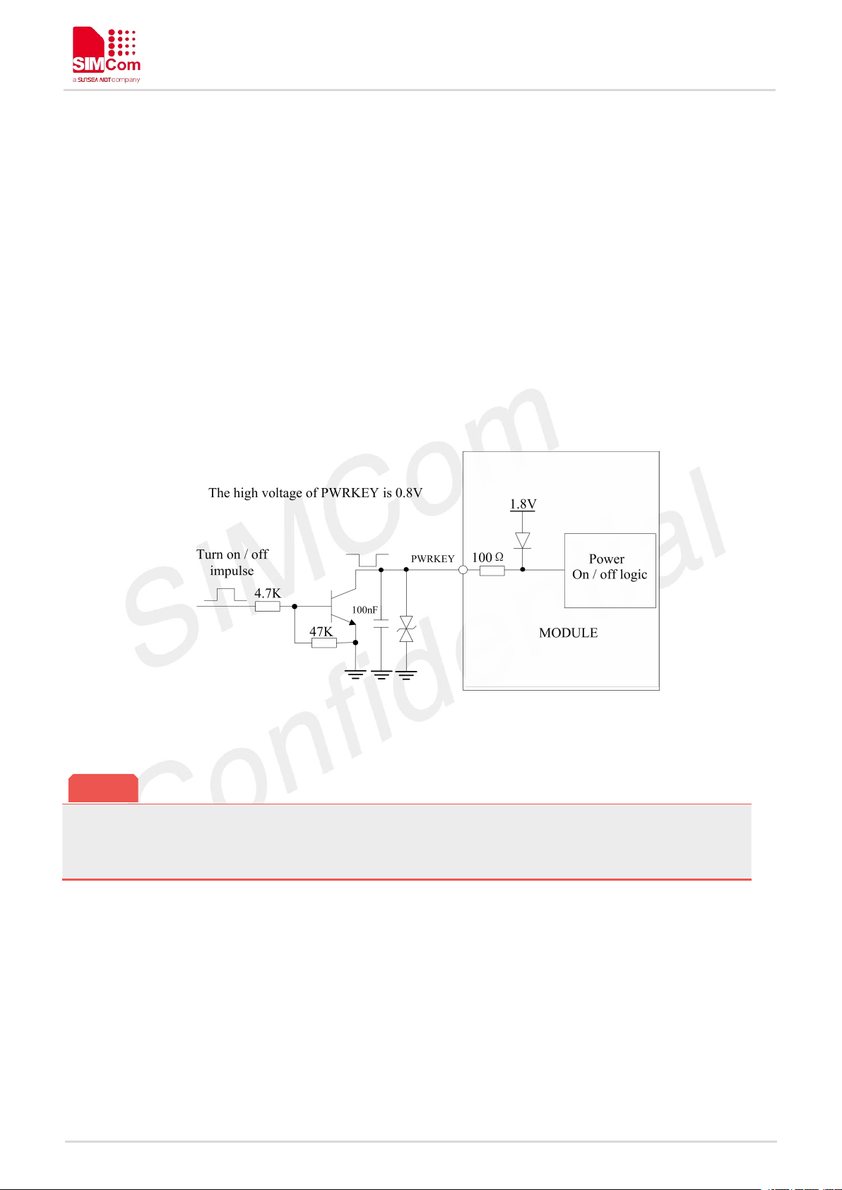
Module could be automatically power on by connecting PWRKEY pin to ground via 0R resistor directly.
NOTE
3.2Power on/Power off/Reset Function
3.2.1 Power on
MODULE can be powered on by pulling the PWRKEY pin down to ground.
The PWRKEY pin has been pulled up with a diode to 1.8V internally, so it does not need to be pulled up
externally. It is strongly recommended to put a100nF capacitor, an ESD protection diode, close to the
PWRKEY pin as it would strongly enhance the ESD performance of PWRKEY pin. Please refer to the
following figure for the recommended reference circuit.
Figure 9: Reference power on/off circuit
The power-on scenarios are illustrated in the following figure.
www.simcom.com
30/75
Page 31
Figure 10: Power on timing sequence
Symbol
Parameter
Min.
Typ.
Max.
Unit
T
on
The time of active low level impulse of PWRKEY pin to
power on MODULE
100
500-ms
T
on(status)
The time from power-on issue to STATUS pin output
high level(indicating power up ready )
1516-
s
T
on(uart)
The time from power-on issue to UART port ready
1314-
s
T
on(vdd_aux)
The time from power-on issue to VDD_AUX ready
2.5-s
T
on(usb)
The time from power-on issue to USB port ready
1112-
s
VIHInput high level voltage on PWRKEY pin
0.6
0.8
1.8
V
VILInput low level voltage on PWRKEY pin
-0.300.5
V
NOTE
SIM7600G-H User manual
Table 8: Power on timing and electronic characteristic
3.2.2 Power off
The following methods can be used to power off MODULE.
● Method 1: Power off MODULE by pulling the PWRKEY pin down to ground.
● Method 2: Power off MODULE by AT command “AT+CPOF”.
● Method 3: over-voltage or under-voltage automatic power off. The voltage range can be set by AT
command “AT+CPMVT”.
● Method 4: over-temperature or under-temperature automatic power off.
www.simcom.com
31/75
Page 32
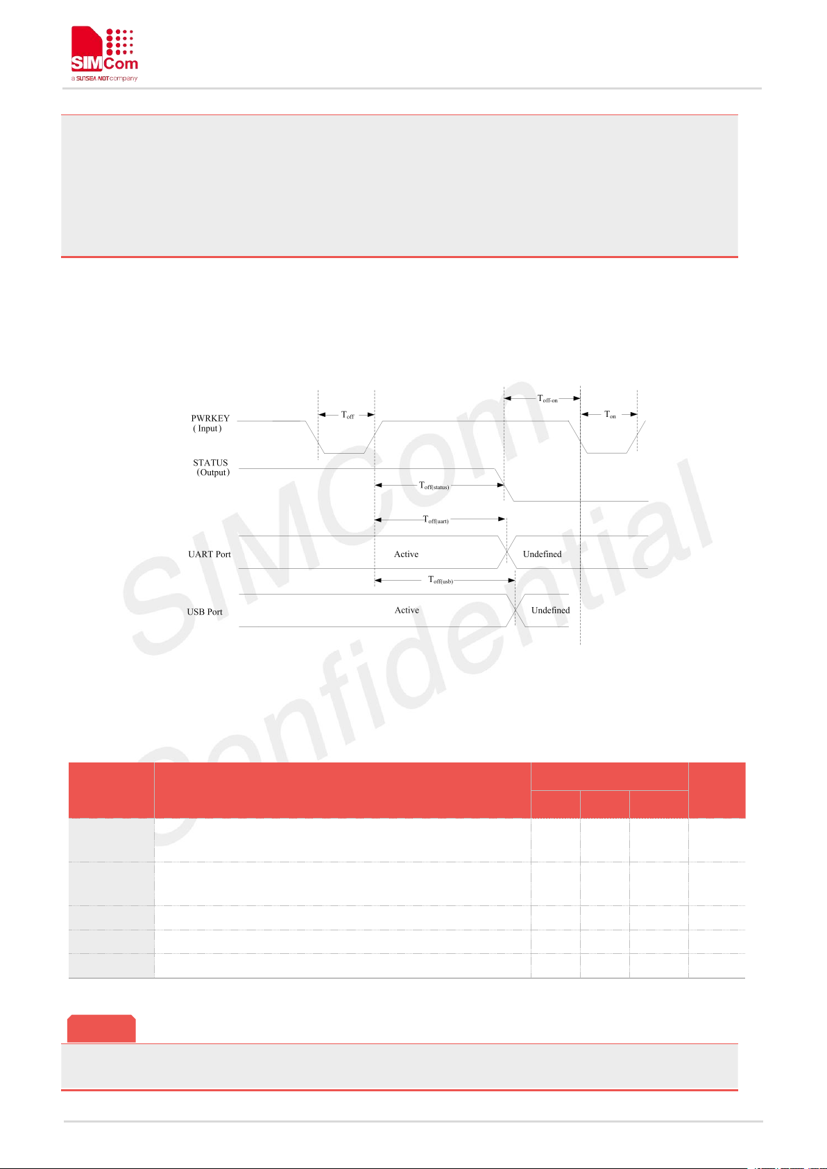
SIM7600G-H User manual
If the temperature is outside the range of -30~+80℃, some warning will be reported via AT port. If the
temperature is outside the range of -40~+85℃, MODULE will be powered off automatically.
For details about “AT+CPOF” and “AT+CPMVT”, please refer to Document [1].
Symbol
Parameter
Time value
Unit
Min.
Typ.
Max.
T
off
The active low level time pulse on PWRKEY pin to
power off MODULE
--
2.5--s
T
off(status)
The time from power-off issue to STATUS pin output low
level(indicating power off )*
2526-
s
T
off(uart)
The time from power-off issue to UART port off
1415-
s
T
off(usb)
The time from power-off issue to USB port off
2728-
s
T
off-on
The buffer time from power-off issue to power-on issue
0--
s
The STATUS pin can be used to detect whether MODULE is powered on or not. When MODULE has
NOTE
These procedures will make MODULE disconnect from the network and allow the software to enter a safe
state, and save data before MODULE be powered off completely.
The power off scenario by pulling down the PWRKEY pin is illustrated in the following figure.
Figure 11: Power off timing sequence
Table 9: Power off timing and electronic characteristic
www.simcom.com
32/75
Page 33
been powered on and firmware goes ready, STATUS will be high level, or else STATUS will still low
level.
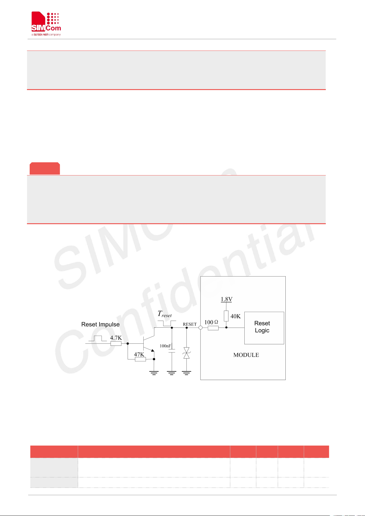
3.2.3 Reset Function
This function is only used as an emergency reset, when AT command “AT+CPOF” and the PWRKEY
pin all have lost efficacy.
Symbol
Description
Min.
Typ.
Max.
Unit
T
reset
The active low level time impulse on RESET pin to
reset MODULE
100
200
500
ms
VIHInput high level voltage
1.17
1.8
2.1
V
NOTE
MODULE can be reset by pulling the RESET pin down to ground.
SIM7600G-H User manual
The RESET pin has been pulled up with a 40KΩ resistor to 1.8V internally, so it does not need to be pulled
up externally. It is strongly recommended to put a100nF capacitor and an ESD protection diode close to the
RESET pin. Please refer to the following figure for the recommended reference circuit.
Figure 12: Reference reset circuit
Table 10: RESET pin electronic characteristic
www.simcom.com
33/75
Page 34
SIM7600G-H User manual
VILInput low level voltage
-0.300.8
V
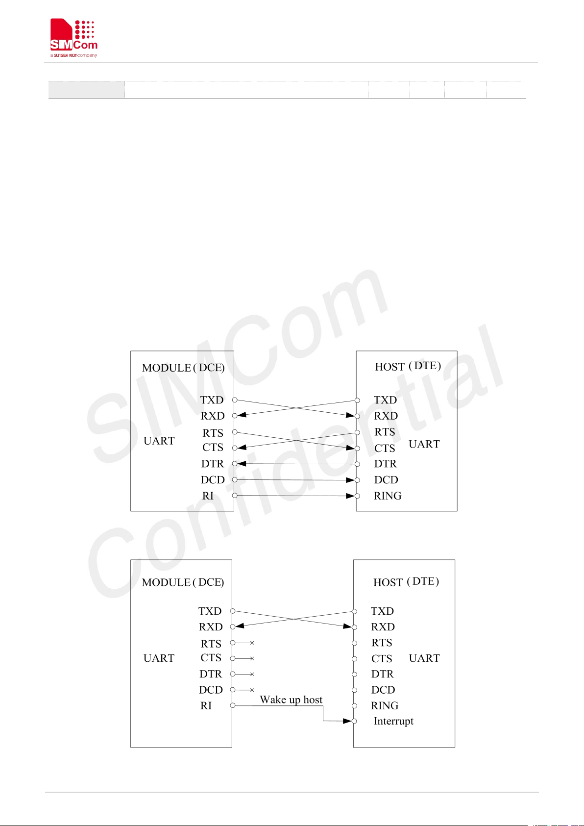
3.3UART Interface
MODULE provides a 7-wire UART (universal asynchronous serial transmission) interface as DCE (Data
Communication Equipment). AT commands and data transmission can be performed through UART
interface.
3.3.1 UART Design Guide
The following figures show the reference design.
www.simcom.com
Figure 13: UART full modem
Figure 14: UART null modem
34/75
Page 35
SIM7600G-H User manual
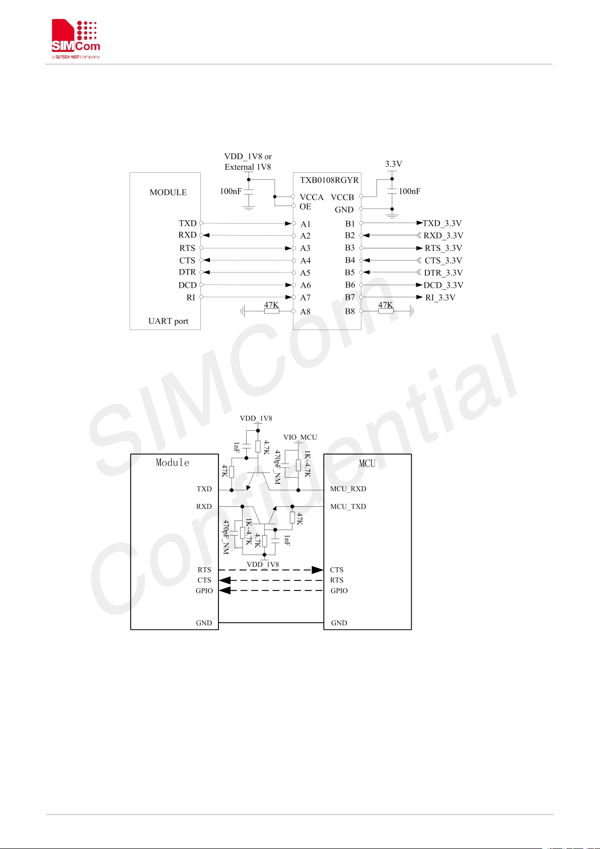
The MODULE UART is 1.8V voltage interface. If user’s UART application circuit is 3.3V voltage interface,
the level shifter circuits should be used for voltage matching. The TXB0108RGYR provided by Texas
Instruments is recommended. The following figure shows the voltage matching reference design.
Figure 15: Reference circuit of level shift
User can use another level shifter circuits as follow
Figure 16: level matching circuit
To comply with RS-232-C protocol, the RS-232-C level shifter chip should be used to connect MODULE to
the RS-232-C interface, for example SP3238ECA, etc.
www.simcom.com
35/75
Page 36

SIM7600G-H User manual
User needs to use high speed transistors such as MMBT3904.
MODULE supports the following baud rates: 300, 600, 1200, 2400, 4800, 9600, 19200, 38400, 57600,
115200, 230400, 460800, 921600, 3200000, 3686400, 4000000bps. The default band rate is
115200bps.
NOTE
NOTE
3.3.2 RI and DTR Behavior
The RI pin can be used to interrupt output signal to inform the host controller such as application CPU.
Normally RI will keep high level until certain conditions such as receiving SMS, or a URC report coming,
and then it will change to low level.
Figure 17: RI behaviour(SMS and URC report)
Normally RI will be kept at a high level until a voice call, then it will output periodic rectangular wave with
5900ms low level and 100ms high level. It will output this kind of periodic rectangular wave until the call is
answered or hung up.
Figure 18 : RI behaviour(voice call)
www.simcom.com
36/75
Page 37

SIM7600G-H User manual
For more details of AT commands about UART, please refer to document [1] and [22].
NOTE
DTR pin can be used to wake MODULE from sleep. When MODULE enters sleep mode, pulling down DTR
can wake MODULE.
3.4USB Interface
The MODULE contains a USB interface compliant with the USB2.0 specification as a peripheral, but the
USB charging function is not supported.
MODULE can be used as a USB device. MODULE supports the USB suspend and resume mechanism
which can reduce power consumption. If there is no data transmission on the USB bus, MODULE will enter
suspend mode automatically, and will be resumed by some events such as voice call, receiving SMS, etc.
Figure 19: USB reference circuit
Because of the high bit rate on USB bus, more attention should be paid to the influence of the junction
capacitance of the ESD component on USB data lines. Typically, the capacitance should be less than 1pF. It
is recommended to use an ESD protection component such as ESD9L5.0ST5G provided by On
Semiconductor (www.onsemi.com ).
D3 is suggested to select the diode with anti-ESD and voltage surge function, or user could add a TVS for
surge clamping. The recommend TVS please refer to table 7.
www.simcom.com
37/75
Page 38

SIM7600G-H User manual
The USB_DN and USB_DP nets must be traced by 90Ohm+/-10% differential impedance.
SIMcom recommend add USB test pads on customer’s EVB board for Product Debug.
HSIC
USB2.0
Signal-ended signaling at 1.2 V
Differential signaling
Two signals – STROBE, DATA
Four wires – Ground, D+, D-, VBUS
Double data rate signaling
Data inferred from differential signaling
HS-USB 480 Mbps only
HS/FS/LS support
Maximum trace length of 10 cm
Maximum cable length of 5 m
No HS chirp protocol
HS chirp protocol
Lower power consumption (digital)
Higher power consumption (analog)
No concept of disconnect
Hot plug/play support
The module HSIC default work as HSIC to LAN function, if user have any other questions ,please
contact simcom for more details.
NOTE
NOTE
3.5HSIC interface
HSIC is a 2-signal source synchronous serial interface which uses 240MHz DDR signaling to provide
High-Speed 480Mbps USB transfers which are 100% host driver compatible with traditional USB
cable-connected topologies. Full-Speed (FS) and Low-Speed (LS) USB transfers are not directly supported
by the HSIC interface (a HSIC enabled hub can provide FS and LS support, as well as IC_USB support)
The differences between HSIC and USB2.0 are listed below:
Table 11: Key differences between HSIC and HS-USB
module implements a HSIC interface compliant with the HSIC1.0 specification which can be used to
connect to the external IC.
www.simcom.com
38/75
Page 39
SIM7600G-H User manual
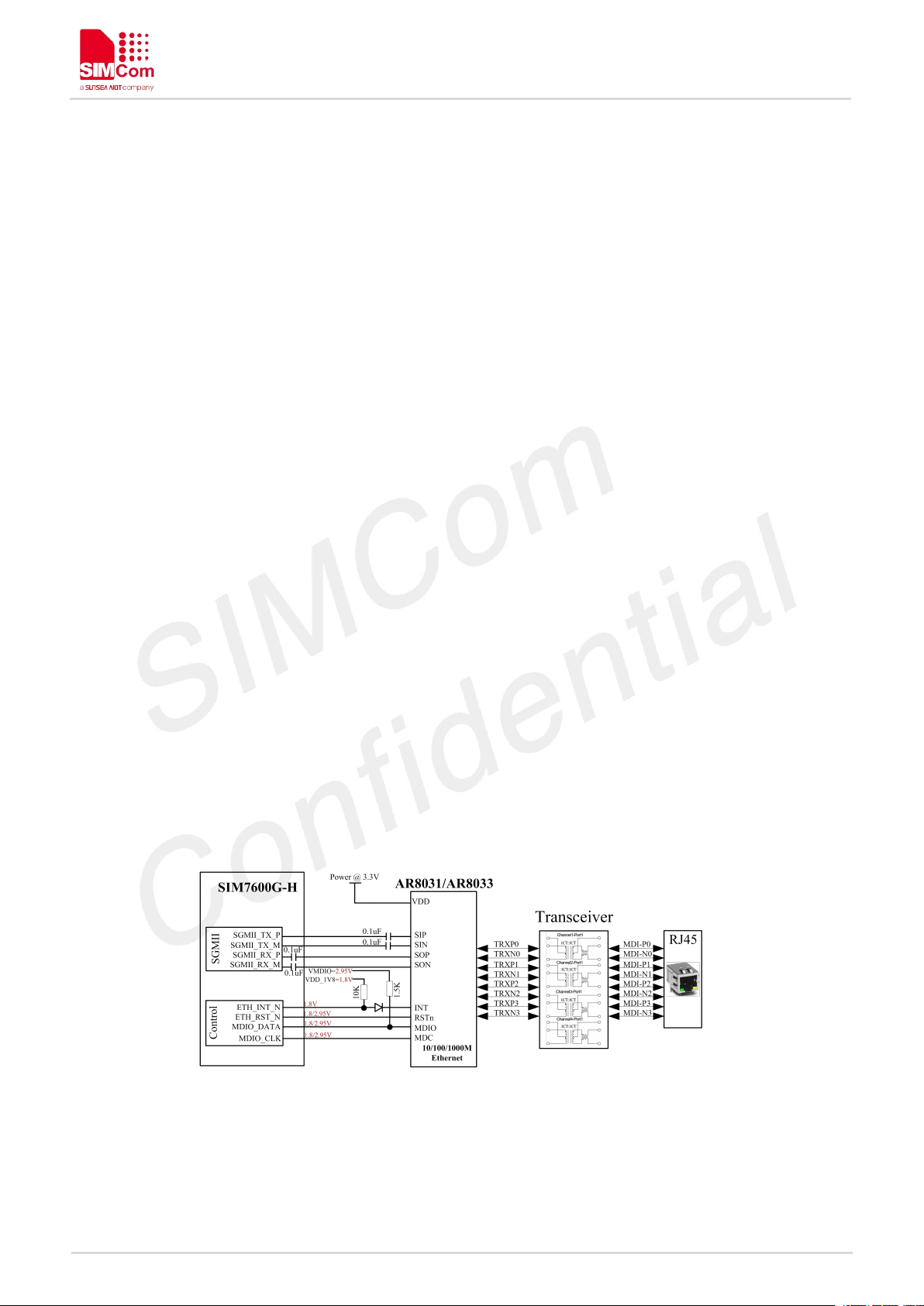
3.6SGMII Interface
MODULE provides a SGMII interface with an Ethernet MAC embedded, users could add a PHY to connect
to the Ethernet, and the PHY device could be controlled by the MDIO interface and other dedicated signals.
Two Ethernet PHY are supported: AR8031/AR8033 (Qualcomm) and BCM89820 (Broadcom). The
AR8031/AR8033 is used for the industrial field and the BCM89820 is dedicated for the automotive field.
Main features of SGMII:
Ethernet Mac integrated in the module
IEEE 802.3 Ethernet 10/100/1000Mbps, SGMII IF
Supports IEEE 1588, Precision Time Protocol (PTP)
Full duplex rated to 1 Gbps
Half/full duplex for 10/100 Mbps
Can be connected to external Ethernet PHY like AR8031/AR8033(industrial 10/100/1000Mbps),
BCM89820(automotive 10/100Mbps)
Uses 8B10B encoding of data with effective baud data rate of 1 Gbps, data rate is always 1.25 Gbps
(or DDR clock is always at 625 MHz)
Main features of MDIO:
Host mode only
Dual voltage: 1.8 V or 2.85 V operation
Default signal frequency: 6.25MHz
MDIO_DATA is OD-gate, and requires an external 1.5 kΩ pull-up resistor to VMDIO.
For the AR8031/AR8033, User should provide 3.3V to power the external Ethernet PHY system and the
current should be more than 200mA.
3.6.1 Reference schematic with AR8033
Figure 20: Reference SGMII circuit with AR8033
For the BCM89820, Users should provide 3.3V and 1.2V to power the external Ethernet PHY system and
the data interface of PHY. The current of 3.3V and 1.2V should be more than 100mA and 150mA.
www.simcom.com
39/75
Page 40
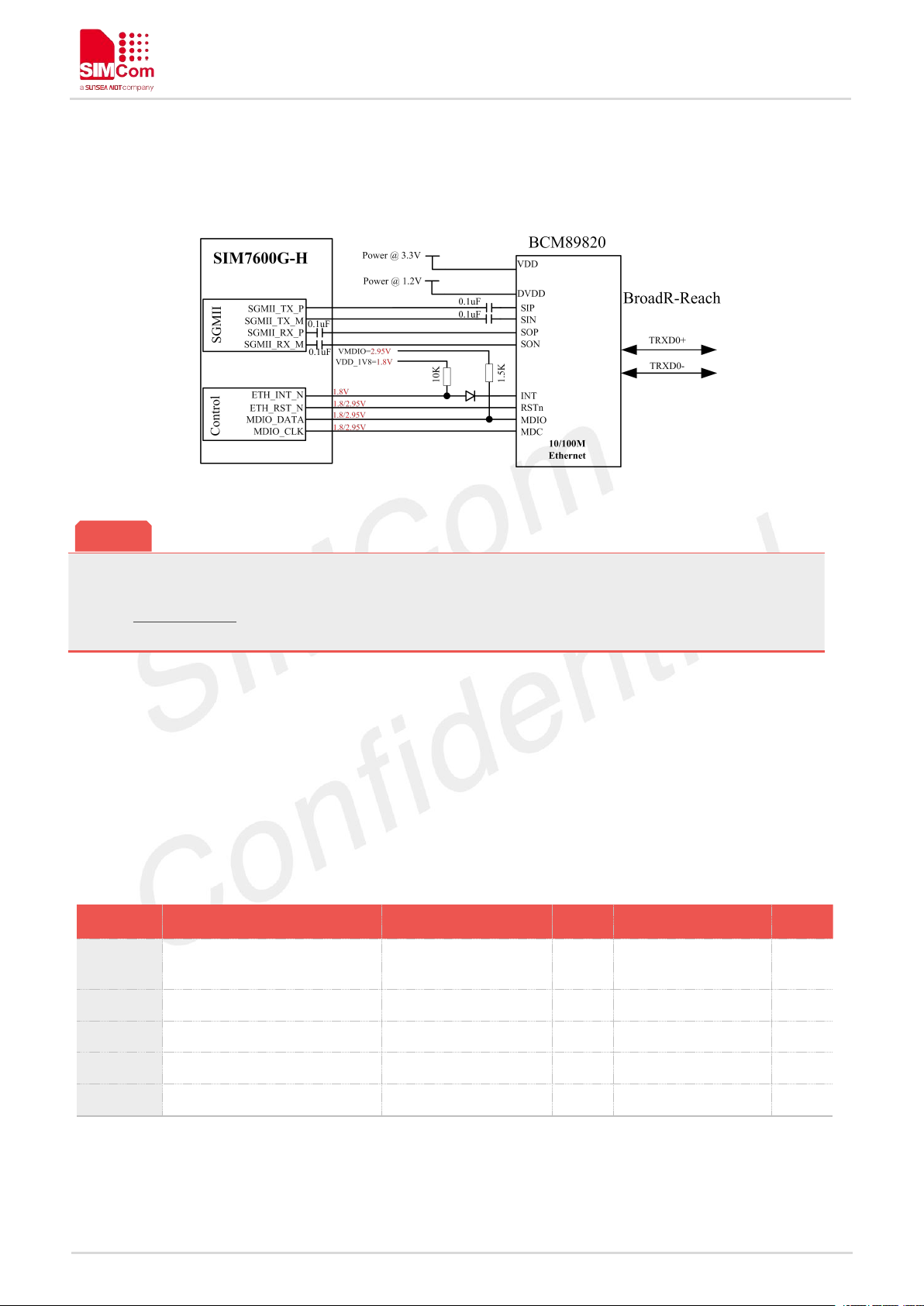
3.6.2 Reference schematic with BCM89820
The module SGMII function default closed. If user need, please contact SIMCom for more details or
refer to document [28]
Symbol
Parameter
Min.
Typ.
Max.
Unit
USIM_V
DD
LDO power output voltage
1.75
1.8
1.95
V
VIHHigh-level input voltage
0.65*USIM_VDD
-
USIM_VDD +0.3
V
VILLow-level input voltage
-0.300.35*USIM_VDD
V
VOHHigh-level output voltage
USIM_VDD -0.45
-
USIM_VDD
V
VOLLow-level output voltage
000.45
V
NOTE
Figure 21: Reference SGMII circuit with BCM89820
SIM7600G-H User manual
3.7USIM Interface
MODULE supports both 1.8V and 3.0V USIM Cards.
Table 12: USIM electronic characteristic in 1.8V mode (USIM_VDD=1.8V)
www.simcom.com
40/75
Page 41
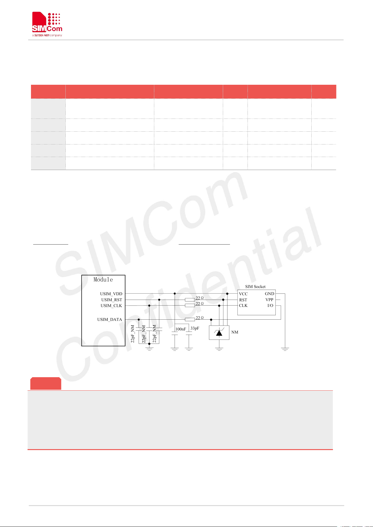
Table 13: USIM electronic characteristic 3.0V mode (USIM_VDD=2.95V)
Symbol
Parameter
Min.
Typ.
Max.
Unit
USIM_V
DD
LDO power output voltage
2.75
2.95
3.05
V
VIHHigh-level input voltage
0.65*USIM_VDD
-
USIM_VDD +0.3
V
VILLow-level input voltage
-0.300.25*USIM_VDD
V
VOHHigh-level output voltage
USIM_VDD -0.45
-
USIM_VDD
V
VOLLow-level output voltage
000.45
V
USIM_DATA has been pulled up with a 10KΩ resistor to USIM_VDD in MODULE. A 100nF capacitor on
USIM_VDD is used to reduce interference. For more details of AT commands about USIM, please refer
to document [1].USIM_CLK is very important signal, the rise time and fall time of USIM_CLK should be
less than 40ns, otherwise the USIM card might not be initialized correctly.
NOTE
3.7.1 USIM Application Guide
SIM7600G-H User manual
It is recommended to use an ESD protection component such as ESDA6V1W5 produced by ST
(www.st.com ) or SMF15C produced by ON SEMI (www.onsemi.com ). Note that the USIM peripheral circuit
should be close to the USIM card socket. The following figure shows the 6-pin SIM card holder reference
circuit.
Figure 22: USIM interface reference circuit
The USIM_DET pin is used for detection of the USIM card hot plug in. User can select the 8-pin USIM card
holder to implement USIM card detection function.
The following figure shows the 8-pin SIM card holder reference circuit.
www.simcom.com
41/75
Page 42

SIM7600G-H User manual
Figure 23: USIM interface reference circuit with USIM_DET
If the USIM card detection function is not used, user can keep the USIM_DET pin open.
SIM card circuit is susceptible, the interference may cause the SIM card failures or some other situations,
so it is strongly recommended to follow these guidelines while designing:
Make sure that the SIM card holder should be far away from the antenna while in PCB layout.
SIM traces should keep away from RF lines, VBAT and high-speed signal lines.
The traces should be as short as possible.
Keep SIM holder’s GND connect to main ground directly.
Shielding the SIM card signal by ground.
Recommended to place a 0.1~1uF capacitor on USIM_VDD line and keep close to the holder.
The rise/fall time of USIM_CLK should not be more than 40ns.
Add some TVS and the parasitic capacitance should not exceed 60pF.
Recommended USIM Card Holder
It is recommended to use the 6-pin USIM socket such as C707 10M006 512 produced by Amphenol. User
can visit http://www.amphenol.com for more information about the holder.
www.simcom.com
42/75
Page 43
Figure 24: Amphenol SIM card socket
Pin
Signal
Description
C1
USIM_VDD
USIM Card Power supply.
C2
USIM_RST
USIM Card Reset.
C3
USIM_CLK
USIM Card Clock.
C5
GND
Connect to GND.
C6
VPP
NC
C7
USIM_DATA
USIM Card data I/O.
For more details about PCM AT commands, please refer to document [1].
Characteristics
Specification
Line Interface Format
Linear(Fixed)
Data length
16bits(Fixed)
PCM Clock/Sync Source
Master Mode(Fixed)
PCM Clock Rate
2048 KHz (Fixed)
PCM Sync Format
Short sync(Fixed)
Data Ordering
MSB
NOTE
Table 14: Amphenol USIM socket pin description
3.8PCM Interface
SIM7600G-H User manual
MODULE provides a PCM interface for external codec, which can be used in master mode with short sync
and 16 bits linear format.
Table 15: PCM format
3.8.1 PCM timing
MODULE supports 2.048 MHz PCM data and sync timing for 16 bits linear format codec.
www.simcom.com
43/75
Page 44

Figure 25: PCM_SYNC timing
Parameter
Description
Min.
Typ.
Max.
Unit
T(sync)
PCM_SYNC cycle time
–
125–μs
T(synch)
PCM_SYNC high level time
–
488–ns
T(syncl)
PCM_SYNC low level time
–
124.5
–
μs
T(clk)
PCM_CLK cycle time
–
488–ns
T(clkh)
PCM_CLK high level time
–
244–ns
T(clkl)
PCM_CLK low level time
–
244–ns
T(susync)
PCM_SYNC setup time high before falling edge of
PCM_CLK
–
244–ns
T(hsync)
PCM_SYNC hold time after falling edge of
PCM_CLK
–
244–ns
T(sudin)
PCM_IN setup time before falling edge of
PCM_CLK
60––
ns
T(hdin)
PCM_IN hold time after falling edge of PCM_CLK
10––
ns
T(pdout)
Delay from PCM_CLK rising to PCM_OUT valid
––60
ns
Figure 26: EXT codec to MODULE timing
SIM7600G-H User manual
Table 16: PCM timing parameters
Figure 27: Module to EXT codec timing
www.simcom.com
44/75
Page 45

T(zdout)
Delay from PCM_CLK falling to PCM_OUT
HIGH-Z
–
160-ns
3.8.2 PCM Application Guide
Symbol
Parameter
Min.
Typ.
Max.
Unit
VIHHigh-level input voltage
0.65*2.85
-
2.85+0.3
V
VILLow-level input voltage
-0.300.25*2.85
V
VOHHigh-level output voltage
0.75*2.85
2.85
2.85
V
VOLLow-level output voltage
000.15*2.85
V
The following figure shows the external codec reference design.
SIM7600G-H User manual
Figure 28: Audio codec reference circuit
3.9SD Interface
MODULE provides a 4-bit SD/MMC/eMMC interface with clock rate up to 200 MHz.
When connected to a SD or MMC card, the voltage of SD interface is 1.8/2.85V, which is compatible with
Secure Digital Physical Layer Specification version 3.0 and SDIO Card Specification version 3.0.It supports
up to 128GB SD cards.
When connected to a eMMC card, the interface voltage will be a sigle 1.8V, which is compatible with eMMC
Specification, version 4.5. It supports up to 128GB eMMC cards.
Table 17: SD/MMC electronic characteristic as 2.85V (SD_DATA0-3,SD_CLK and SD_CMD)
www.simcom.com
45/75
Page 46

SIM7600G-H User manual
Symbol
Parameter
Min.
Typ.
Max.
Unit
VIHHigh-level input voltage
0.7*1.8
-
1.8+0.2
V
VILLow-level input voltage
-0.300.3*1.8
V
VOHHigh-level output voltage
1.8-0.4
1.8
1.8
V
VOLLow-level output voltage
000.45
V
Table 18: SD/MMC/eMMC electronic characteristic as 1.8V (SD_DATA0-3,SD_CLK and SD_CMD)
Users should provide 2.85V to power SD card system and the current should more than 350mA, which is
showed below as VCC_SD. ESD/EMI components should be arranged beside SD card socket. Refer to the
following application circuit.
Figure 29: SD reference circuit
Users should provide 2.85V to power eMMC card system and 1.8V to power the SDIO_DATA/CMD/CLK
signals. The source of 2.85V should be able to provide more than 500mA* which showed below as
VCC_eMMC, as the source of 1.8V should be able to provide more than 300mA* which showed below as
VCCQ_1V8. ESD/EMI components should be arranged close to the eMMC card. Refer to the following
application circuit.
www.simcom.com
46/75
Page 47

Figure 30: eMMC reference circuit
For the current of VCC_eMMC and VCCQ_1V8, users should better refer to the related datasheet of
eMMC which is used. The listed current of 500mA and 300mA are just for your reference.
NOTE
SIM7600G-H User manual
SD/MMC/eMMC card layout guide lines:
● Protect SD card signals from noisy signals (clocks, SMPS, etc.).
● Up to 200 MHz clock rate, 50 Ω nominal, ±10% trace impedance
● CLK to DATA/CMD length matching < 1 mm
● Total routing length < 50 mm
● Spacing to all other signals = 2x line width
● Bus capacitance < 10 pF
3.10 I2C Interface
MODULE provides a I2C interface compatible with I2C specification, version 5.0, with clock rate up to 400
kbps. Its operation voltage is 1.8V.
The following figure shows the I2C bus reference design.
www.simcom.com
47/75
Page 48
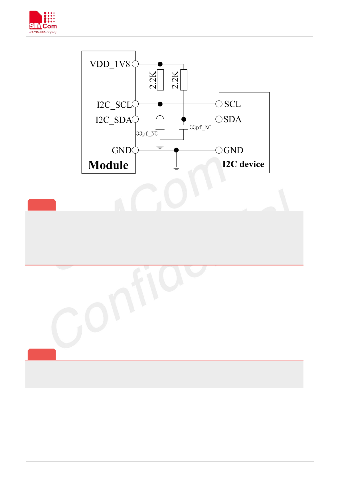
Figure 31: I2C reference circuit
SDA and SCL do not have pull-up resistors in MODULE. So, 2 external pull up resistors are needed in
application circuit.
“AT+CRIIC and AT+CWIIC” AT commands could be used to read/write register values of the I2C
peripheral devices. For more details about AT commands please refer to document [1].
Special software version for CAT4 MODULEs supports this function.
NOTE
NOTE
SIM7600G-H User manual
3.11 SDIO Interface
MODULE provides a 4 bit 1.8V SDIO interface for WLAN solution with W58 module.
The SDIO interface can be used for WLAN solution.
3.12 SPI Interface
Module provides a SPI interface as a master only. It provides a duplex, synchronous, serial communication
www.simcom.com
48/75
Page 49

SIM7600G-H User manual
For more details of the AT commands about the SPI, please refer to document [1].
The value of the resistor named “R” depends on the LED characteristic.
NETLIGHT pin status
Module status
Always On
Searching Network; Call Connect(include VOLTE,SRLTE)
NOTE
NOTE
link with peripheral devices. Its operation voltage is 1.8V, with clock rates up to 50 MHz
3.13 Network status
The NETLIGHT pin is used to control Network Status LED, its reference circuit is shown in the following
figure.
Figure 32: NETLIGHT reference circuit
Table 19: NETLIGHT pin status
www.simcom.com
49/75
Page 50
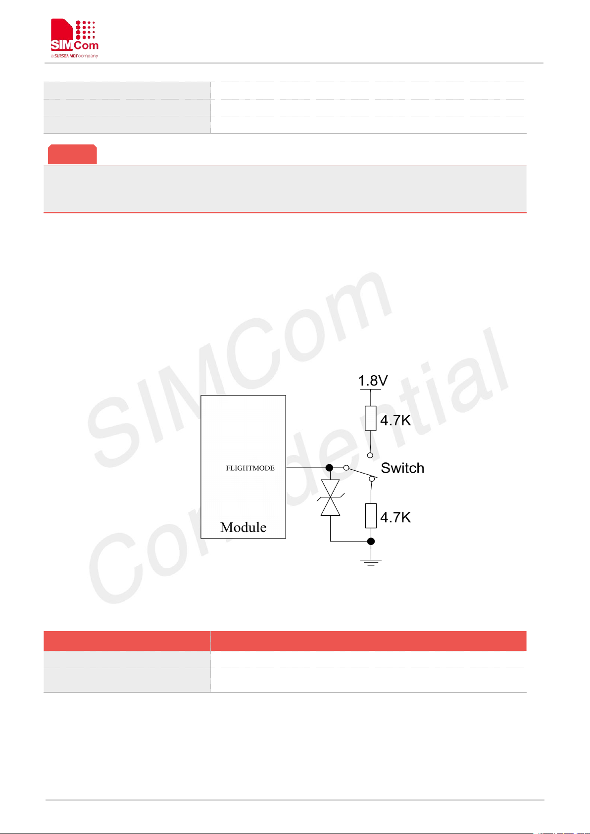
SIM7600G-H User manual
200ms ON, 200ms OFF
Data Transmit; 4G registered;
800ms ON, 800ms OFF
2G/3G registered network
OFF
Power off ;Sleep
NETLIGHT output low level as “OFF”, and high level as “ON”.
FLIGHTMODE pin status
Module operation
Input Low Level
Flight Mode: RF is closed
Input High Level
AT+CFUN=0: RF is closed
AT+CFUN=1:RF is working
NOTE
3.14 Flight Mode Control
The FLIGHTMODE pin can be used to control MODULE to enter or exit the Flight mode. In Flight mode, the
RF circuit is closed to prevent interference with other equipments and minimize current consumption.
Bidirectional ESD protection component is suggested to add on FLIGHTMODE pin, its reference circuit is
shown in the following figure.
Figure 33: Flight mode switch reference circuit
Table 20: FLIGHTMODE pin status
www.simcom.com
50/75
Page 51

SIM7600G-H User manual
Symbol
Description
Min.
Typ.
Max.
Unit
V
ISINK
Voltage tolerant
0.5-VBAT
V
I
ISINK
Current tolerant
0-40
mA
The sinking current can be adjusted to meet the design requirement through the AT command “AT+
CLEDITST =<0>, <value>”.The “value” ranges from 0 to 8, on behalf of the current from 0mA to 40mA
by 5mA step.
NOTE
3.15 Other interface
3.15.1 Sink Current Source
The ISINK pin is VBAT tolerant and intended to drive some passive devices, such as LCD backlight and
white LED, etc. Its output current can be up to 40mA and be set by the AT command “AT+ CLEDITST”.
Table 21: Sink current electronic characteristic
ISINK is a ground-referenced current sink. The following figure shows its reference circuit.
Figure 34: ISINK reference circuit
www.simcom.com
51/75
Page 52
SIM7600G-H User manual
Characteristics
Min.
Typ.
Max.
Unit
Resolution
–15–
Bits
Conversion time
–
442–ms
Input Range
0.1
1.7
V
Input serial resistance
1––
MΩ
“AT+CADC” and “AT+CADC2” can be used to read the voltage of the ADC1 and ADC2 pins, for more
details, please refer to document [1].
Symbol
Description
Min.
Typ.
Max.
Unit
V
VDD_AUX
Output voltage
1.7
2.85
3.05
V
IOOutput current
--150
mA
For more details of AT commands about VDD_AUX, please refer to document [1].
NOTE
NOTE
3.15.2 ADC
MODULE has 2 dedicated ADC pins named ADC1 and ADC2.They are available for digitizing analog
signals such as battery voltage and so on. These electronic specifications are shown in the following table.
Table 22: ADC1 and ADC2 electronic characteristics
3.15.3 LDO
MODULE has a LDO power output, named VDD_AUX. its output voltage is 2.85V by default, Users can
switch the LDO on or off by the AT command “AT+CVAUXS” and configure its output voltage by the AT
command “AT+CVAUXV”.
Table 23: Electronic characteristic
www.simcom.com
52/75
Page 53

4 RF Specifications
Frequency
Power
Min.
LTE-FDD B2
23dBm +/-2.7dB
<-40dBm
LTE-FDD B4
23dBm +/-2.7dB
<-40dBm
LTE-FDD B5
23dBm +/-2.7dB
<-40dBm
LTE-FDD B12
23dBm +/-2.7dB
<-40dBm
LTE-FDD B13
23dBm +/-2.7dB
<-40dBm
LTE-FDD B25
23dBm +/-2.7dB
<-40dBm
LTE-FDD B26
23dBm +/-2.7dB
<-40dBm
LTE-FDD B66
23dBm +/-2.7dB
<-40dBm
LTE-TDD B41
23dBm +/-2.7dB
<-40dBm
Frequency
Receiving
Transmission
The LTE Operating frequencies are shown in the following table 24.
Note: Operating frequencies of LTE TDD B41 for the MODULE is 200MHz BW, 2496~
2690 MHz
GPS
1574.4 ~1576.44 MHz
-
GLONASS
1598 ~1606 MHz
-
BD
1559 ~1563 MHz
E-UTRA
Operating
Band
Uplink (UL) operating
band
Downlink (DL) operating
band
Duplex
Mode
4.1. GSM/UMTS/LTE RF Specifications
Table 24: Conducted transmission power
SIM7600G-H User manual
Table 25: Operating frequencies
Table 26: E-UTRA operating bands
www.simcom.com
53/75
Page 54

2
1850~1910 MHz
1930~1990 MHz
FDD
4
1710~1755MHz
2110~2155MHz
FDD
5
824~849 MHz
869~894MHz
FDD
12
699~716MHz
728~746MHz
FDD
13
777~787MHz
746~757MHz
FDD
25
1850~1915MHz
1930~1995MHz
FDD
26
814~849MHz
859~894MHz
FDD
66
1710~1780MHz
2110~2200MHz
FDD
41
2496~2696 MHz
2496~2696 MHz
TDD
Table 27: Conducted receive sensitivity
Frequency
Receive sensitivity(Typical)
Receive sensitivity(MAX)
LTE FDD/TDD
See table 26.
3GPP
E-UTR
A band
1.4 MHz
Standar
d
3 MHz
Standar
d
5 MHz
Standar
d
10 MHz
Standar
d
15 MHz
Standard
20 MHz
Standar
d
Duplex
Mode
2
-102.7
-99.7
-98
-95
-93.2
-92
FDD
4
-104.7
-101.7
-100
-97
-95.2
-94
FDD
5
-103.2
-100.2
-98
-95
FDD
12
-101.7
-98.7
-97
-94
FDD
13
-97
-94
FDD
25
-101.2
-98.2
-96.5
-93.5
-91.7
-90.5
FDD
26
-102.7
-99.7
-97.5
-94.5
-92.7
FDD
66
-104.7
-101.7
-100
-97
-95.2
-94
FDD
41--
-99
-96
-94.2
-93
TDD
Frequency
Loss
SIM7600G-H User manual
Table 28: Reference sensitivity (QPSK)
4.2. LTE Antenna Design Guide
Users should connect antennas to MODULE’s antenna pads through micro-strip line or other types of RF
trace and the trace impedance must be controlled in 50Ω. SIMCom recommends that the total insertion loss
between the antenna pads and antennas should meet the following requirements:
Table 29: Trace loss
www.simcom.com
54/75
Page 55

SIM7600G-H User manual
700MHz-960MHz
<0.5dB
1710MHz-2170MHz
<0.9dB
2300MHz-2650MHz
<1.2dB
To facilitate the antenna tuning and certification test, a RF connector and an antenna matching circuit
should be added. The following figure is the recommended circuit.
Figure 35: Antenna matching circuit (MAIN_ANT)
In above figure, the components R1, C1, C2 and R2 are used for antenna matching, the values of
components can only be achieved after the antenna tuning and usually provided by antenna vendor. By
default, the R1, R2 are 0Ω resistors, and the C1, C2 are reserved for tuning. The component D1 is a TVS
for ESD protection, and it is optional for users according to application environment.
The RF test connector is used for the conducted RF performance test, and should be placed as close as to
the MODULE’s MAIN_ANT pin. The traces impedance between MODULE and antenna must be controlled
in 50Ω.
In above figure, R3, C3, C4 and R4 are used for auxiliary antenna matching. By default, the R3, R4 are
0Ωresistors, and the C3, C4 are reserved for tuning. D2 is a TVS for ESD protection, and it is optional for
users according to application environment.
www.simcom.com
Figure 36: Antenna matching circuit (AUX_ANT)
55/75
Page 56
Two TVS are recommended in the table below.
Package
Part Number
Vender
0201
LXES03AAA1-154
Murata
0402
LXES15AAA1-153
Murata
SIMCom suggests the LTE auxiliary antenna to be kept on, since there are many high bands in the
designing of LTE-TDD, such as band41. Because of the high insert loss of the RF cable and layout
lines, the receiver sensitivity of these bands above will have risk to meet the authentication without the
diversity antenna. For more details about auxiliary antenna design notice, please refer to document
[25].
NOTE
NOTE
Table 30: Recommended TVS
SIM7600G-H User manual
4.3. GNSS
MODULE merges GNSS (GPS/GLONASS/BD) satellite and network information to provide a
high-availability solution that offers industry-leading accuracy and performance. This solution performs well,
even in very challenging environmental conditions where conventional GNSS receivers fail, and provides a
platform to enable wireless operators to address both location-based services and emergency mandates.
4.3.1 GNSS Technical specification
Tracking sensitivity: -159 dBm(GPS)/-158 dBm(GLONASS)/-159 dBm(BD)
Cold-start sensitivity: -148 dBm
Accuracy (Open Sky): 2.5m (CEP50)
TTFF (Open Sky) : Hot start <1s, Cold start<35s
Receiver Type: 16-channel, C/A Code
GPS L1 Frequency: 1575.42±1.023MHz
GLONASS: 1597.5~1605.8 MHz
BD: 1559.05~1563.14 MHz
Update rate: Default 1 Hz
GNSS data format: NMEA-0183
GNSS Current consumption : 100mA (GSM/UMTS/LTE Sleep ,in total on VBAT pins)
GNSS antenna: Passive/Active antenna
www.simcom.com
56/75
Page 57

SIM7600G-H User manual
If the antenna is active type, the power should be given by main board because there is no power
supply on the GPS antenna pad. If the antenna is passive, it is suggested that the external LNA should
be used.
4.3.2 GNSS Application Guide
Users can adopt an active antenna or a passive antenna to MODULE. If using a passive antenna, an
external LNA is a must to get better performance.
The following figures are the reference circuits.
Figure 37: Active antenna circuit
Figure 38: Passive antenna circuit (Default)
In above figures, the components C1, L1 and L2 are used for antenna matching. Usually, the values of the
components can only be achieved after antenna tuning and usually provided by antenna vendor. C2 is used
for DC blocking. L3 is the matching component of the external LNA, and the value of L3 is determined by
the LNA characteristic and PCB layout. Both VDD of active antenna and V_LNA need external power
supplies which should be considered according to active antenna and LNA characteristic. LDO/DCDC is
recommended to get lower current consuming by shutting down active antennas and LNA when GNSS is
www.simcom.com
57/75
Page 58

SIM7600G-H User manual
GNSS is closed by default and can be started by AT+CGPS. The AT command has two parameters, the
first is on/off, and the second is GNSS mode. Default mode is standalone mode.
AGPS mode needs more support from the mobile telecommunication network. Please refer to
document [24] for more details.
NOTE
not working.
GNSS can be tested by NMEA port. NMEA sentences can be obtained through UART or USB automatically.
NMEA sentences include GSV, GGA, RMC, GSA, and VTG. Before using GNSS, user should configure
MODULE in proper operating mode by AT command. Please refer to related documents for details.
MODULE can also get position location information through AT directly.
Note: GNSS is closed by default and can be started by AT+CGPS. The AT command has two parameters,
the first is on/off, and the second is GNSS mode. Default mode is standalone mode.
AGPS mode needs more support from the mobile telecommunication network. Please refer to document
[24] for more details.
www.simcom.com
58/75
Page 59
SIM7600G-H User manual
Parameter
Min.
Typ.
Max.
Unit
Voltage at VBAT
-0.5-6.0
V
Voltage at USB_VBUS
-0.5-5.85
V
Voltage at digital pins
(RESET,SPI,Keypad,GPIO,I2C,UART,PCM)
-0.3-2.1
V
Voltage at digital pins (SD,USIM)
-0.3-3.05
V
Voltage at PWRKEY
-0.3-1.8
Parameter
Min.
Typ.
Max.
Unit
Voltage at VBAT
3.4
3.8
4.2
V
Voltage at USB_VBUS
3.0
5.0
5.25
V
Parameter
Description
Min.
Typ.
Max.
Unit
VIHHigh-level input voltage
1.17
1.8
2.1
V
VILLow-level input voltage
-0.300.63
V
VOHHigh-level output voltage
1.35
-
1.8VVOLLow-level output voltage
0-0.45
V
5 Electrical Specification
5.1 Absolute maximum ratings
Absolute maximum rating for digital and analog pins of MODULE are listed in the following table:
Table 31: Absolute maximum ratings
5.2 Operating conditions
Table 32: Recommended operating ratings
Table 33: 1.8V Digital I/O characteristics*
www.simcom.com
59/75
Page 60

I
OH
High-level output current(no pull
down resistor)
-2-
mA
I
OL
Low-level output current(no pull
up resistor)
--2-
mA
I
IH
Input high leakage current (no
pull down resistor)
--1
uA
I
IL
Input low leakage current(no pull
up resistor)
-1--
uA
These parameters are for digital interface pins, such as SPI, GPIOs (NETLIGHT, FLIGHTMODE,
STATUS, USIM_DET, SD_DET), SDIO, I2C, UART, PCM, COEXn, and BOOT_CFG0.
The operating temperature of MODULE is listed in the following table.
Parameter
Min.
Typ.
Max.
Unit
Normal operation temperature
-302580
℃
Extended operation temperature*
-402585
℃
Storage temperature
-4525+90
℃
Module is able to make and receive voice calls, data calls, SMS and make GSM/ UMTX/LTE traffic in
-40 ℃ ~ +85 ℃ . The performance will be reduced slightly from the 3GPP specifications if the
temperature is outside the normal operating temperature range and still within the extreme operating
temperature range.
NOTE
NOTE
SIM7600G-H User manual
Table 34: Operating temperature
5.3 Operating Mode
5.3.1. Operating Mode Definition
The table below summarizes the various operating modes of MODULE product.
www.simcom.com
60/75
Page 61

Table 35: Operating mode Definition
Mode
Function
Normal operation
LTE Sleep
In this case, the current consumption of MODULE will be reduced to
the minimal level and the MODULE can still receive paging message
and SMS.
LTE Idle
Software is active. Module is registered to the network, and the
MODULE is ready to communicate.
LTE Talk
Connection between two subscribers is in progress. In this case, the
power consumption depends on network settings such as DTX off/on,
FR/EFR/HR, hopping sequences, and antenna.
LTE Standby
Module is ready for data transmission, but no data is currently sent or
received. In this case, power consumption depends on network
settings.
LTE Data
transmission
There is data transmission in progress. In this case, power
consumption is related to network settings (e.g. power control level);
uplink/downlink data rates, etc.
Minimum functionality mode
AT command “AT+CFUN=0” AT+CSCLK=1 can be used to set the
MODULE to a minimum functionality mode without removing the power
supply. In this mode, the RF part of the MODULE will not work and the
USIM card will not be accessible, but the serial port and USB port are
still accessible. The power consumption in this mode is lower than
normal mode.
Flight mode
AT command “AT+CFUN=4” or pulling down the FLIGHTMODE pin
can be used to set the MODULE to flight mode without removing the
power supply. In this mode, the RF part of the MODULE will not work,
but the serial port and USB port are still accessible. The power
consumption in this mode is lower than normal mode.
Power off
Module will go into power off mode by sending the AT command
“AT+CPOF” or pull down the PWRKEY pin, normally. In this mode the
power management unit shuts down the power supply, and software is
not active. The serial port and USB are is not accessible.
SIM7600G-H User manual
5.3.2. Sleep mode
In sleep mode, the current consumption of MODULE will be reduced to the minimal level, and MODULE can
still receive paging message and SMS.
Several hardware and software conditions must be satisfied together in order to let MODULE enter into
sleep mode:
1. UART condition
2. USB condition
www.simcom.com
61/75
Page 62

SIM7600G-H User manual
Before designing, pay attention to how to realize sleeping/waking function and refer to Document [26]
for more details.
GNSS
GNSS supply current
(AT+CFUN=0,with USB connection)
@ -140dBm,Tracking Typical:38ma
LTE sleep/idle mode
LTE supply current
(GNSS off,without USB connection)
Sleep mode Typical: 2.04ma
Idle mode Typical: 17.3ma
NOTE
3. Software condition
5.3.3. Minimum functionality mode and Flight mode
Minimum functionality mode ceases a majority function of MODULE, thus minimizing the power
consumption. This mode is set by the AT command which provides a choice of the functionality levels.
● AT+CFUN=0: Minimum functionality
● AT+CFUN=1: Full functionality (Default)
● AT+CFUN=4: Flight mode
If MODULE has been set to minimum functionality mode, the RF function and USIM card function will be
closed. In this case, the serial port and USB are still accessible, but RF function and USIM card will be
unavailable.
If MODULE has been set to flight mode, the RF function will be closed. In this case, the serial port and USB
are still accessible, but RF function will be unavailable.
When MODULE is in minimum functionality or flight mode, it can return to full functionality by the AT
command “AT+CFUN=1”.
5.4 Current Consumption
The current consumption is listed in the table below.
Table 36: Current consumption on VBAT Pins (VBAT=3.8V)
www.simcom.com
62/75
Page 63
SIM7600G-H User manual
LTE data
LTE-FDD B2
@5MHz 22.1dBm Typical: 676 ma
@10MHz 22.4dBm Typical: 723 ma
@20MHz 22.3dBm Typical: 759 ma
LTE-FDD B4
@5MHz 22.0dBm Typical: 709 ma
@10MHz 22.1dBm Typical:769 ma
@20MHz 22.6dBm Typical: 896 ma
LTE-FDD B5
@5MHz 22.2dBm Typical: 619 ma
@10MHz 22.1dBm Typical: 628 ma
LTE-FDD B12
@5MHz 22.7dBm Typical: 600 ma
@10MHz 22.7dBm Typical: 607 ma
LTE-FDD B13
@5MHz 21.9dBm Typical: 685 ma
@10MHz 22.0dBm Typical: 653 ma
LTE-FDD B25
@5MHz 22dBm Typical: 634 ma
@10MHz 22dBm Typical: 702 ma
@20MHz 22dBm Typical: 781 ma
LTE-FDD B26
@5MHz 22.4dBm Typical: 615 ma
@10MHz 22.7dBm Typical:664 ma
@15MHz 22.3dBm Typical:713 ma
LTE-FDD B66
@5MHz 22dBm Typical: 707ma
@10MHz 22dBm Typical: 728ma
@20MHz 22dBm Typical: 795 ma
LTE-TDD B41
@5MHz 21.6dBm Typical:803 ma
@10MHz 21.7dBm Typical: 771 ma
@20MHz 21.7dBm Typical: 793 ma
Part
Contact discharge
Air discharge
VBAT,GND
+/-5K
+/-10K
Antenna port
+/-4K
+/-8K
Other PADs
+/-0.5K
+/-1K
5.5 ESD Notes
MODULE is sensitive to ESD in the process of storage, transporting, and assembling. When MODULE is
mounted on the users’ mother board, the ESD components should be placed beside the connectors which
human body may touch, such as USIM card holder, audio jacks, switches, keys, etc. The following table
shows the MODULE ESD measurement performance without any external ESD component.
Table 37: The ESD performance measurement table (Temperature: 25℃, Humidity: 45%)
www.simcom.com
63/75
Page 64
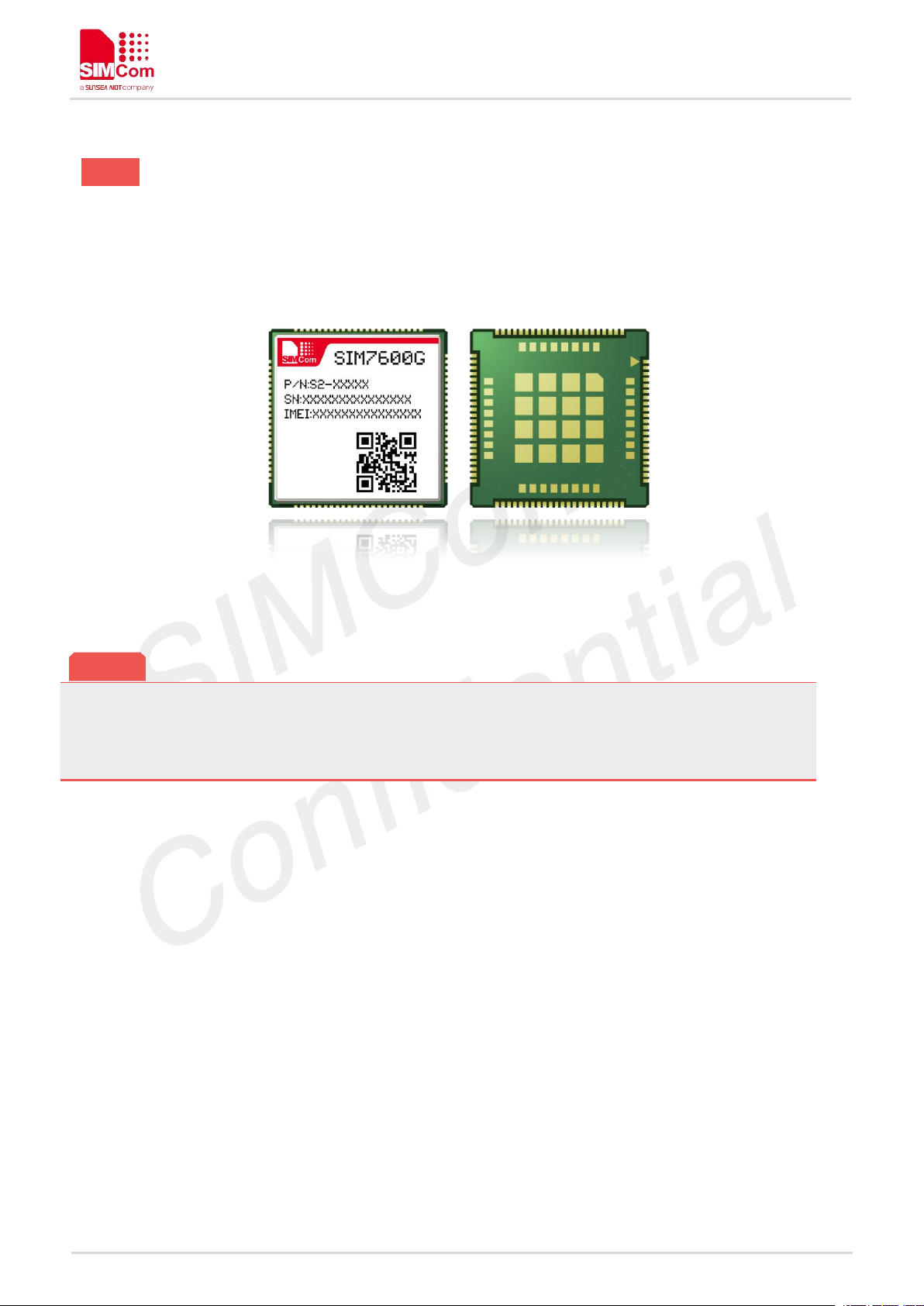
6 SMT Production Guide
The above is the design effect diagram of the module for reference. The actual appearance is subject to
the actual product.
NOTE
6.1 Top and Bottom View of MODULE
SIM7600G-H User manual
Figure 39: Top and bottom view of MODULE
www.simcom.com
64/75
Page 65

6.2 Label Information
No.
Description
A
LOGO
B
Module part number
C
Project name
D
Serial number
E
International mobile equipment identity
SIM7600G-H User manual
Figure 40: Label information
Table 38: The description of label information
6.3 Typical SMT Reflow Profile
SIMCom provides a typical soldering profile. Therefore the soldering profile shown below is only a generic
recommendation and should be adjusted to the specific application and manufacturing constraints.
www.simcom.com
65/75
Page 66
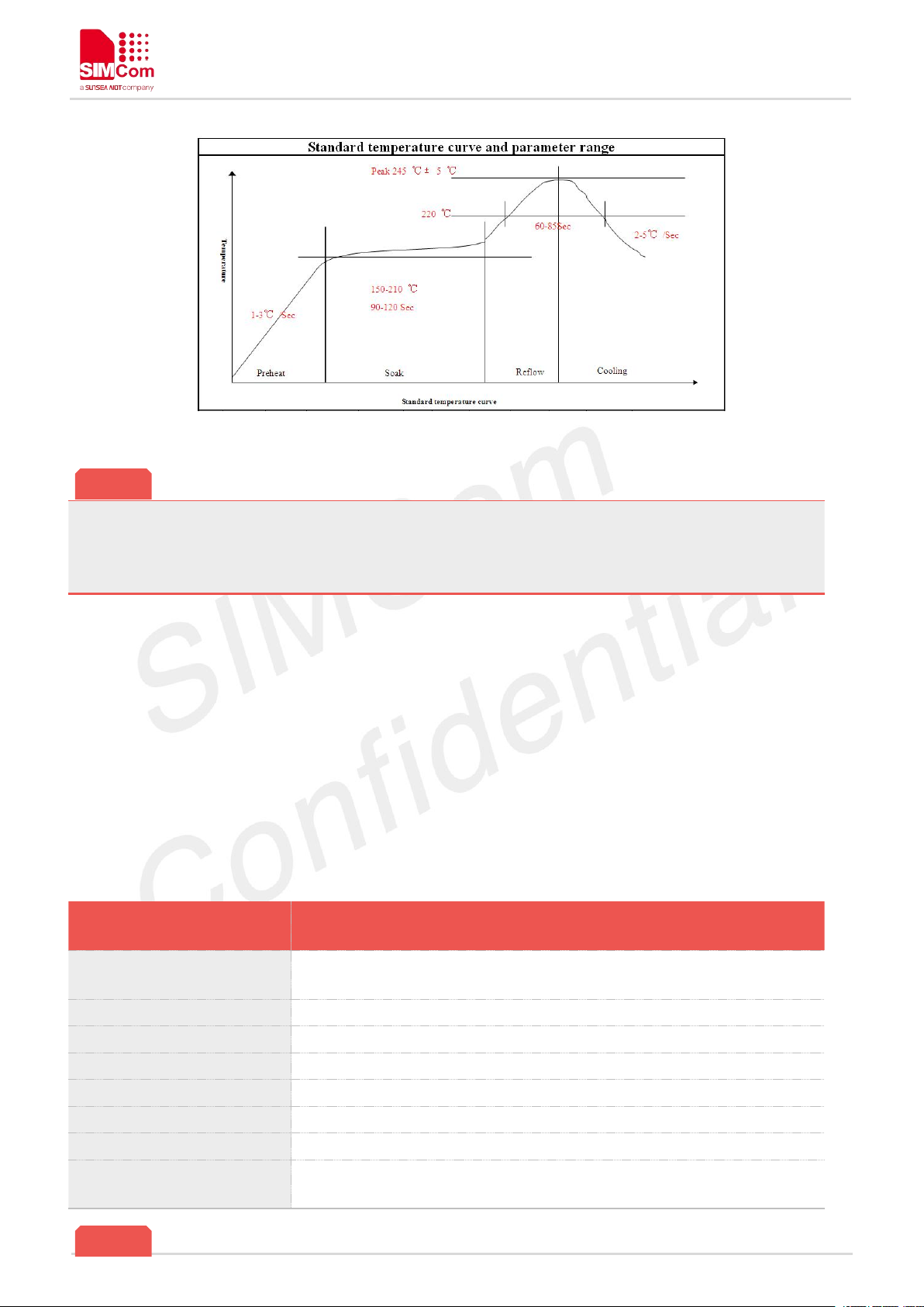
SIM7600G-H User manual
For more details about secondary SMT, please refer to the document [21].
Moisture Sensitivity
Level (MSL)
Floor Life (out of bag) at factory ambient≤30°C/60% RH or
as stated
1
Unlimited at ≦30℃/85% RH
2
1 year
2a
4 weeks
3
168 hours
4
72 hours
5
48 hours
5a
24 hours
6
Mandatory bake before use. After bake, it must be reflowed within the
time limit specified on the label.
NOTE
NOTE
Figure 41: The ramp-soak-spike reflow profile of MODULE
6.4 Moisture Sensitivity Level (MSL)
MODULE is qualified to Moisture Sensitivity Level (MSL) 3 in accordance with JEDEC J-STD-033. If the
prescribed time limit is exceeded, users should bake MODULE for 192 hours in drying equipment (<5% RH)
at 40+5/-0°C, or 72 hours at 85+5/-5°C. Note that plastic tray is not heat-resistant, and only can be baked at
45° C.
Table 39: Moisture Sensitivity Level and Floor Life
www.simcom.com
66/75
Page 67
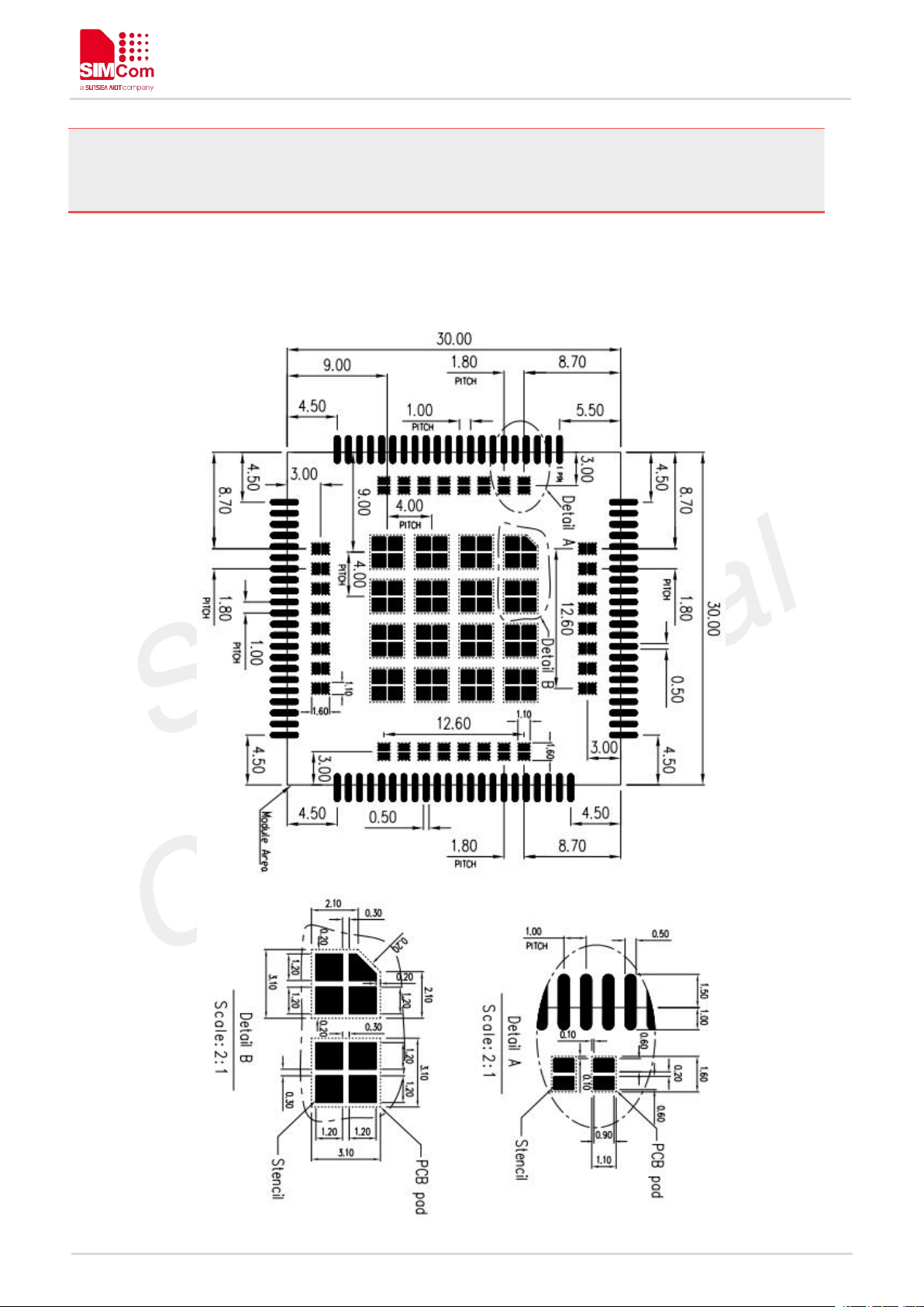
IPC / JEDEC J-STD-033 standard must be followed for production and storage.
6.5 Stencil Foil Design Recommendation
The recommended thickness of stencil foil is more than 0.15mm.
SIM7600G-H User manual
www.simcom.com
67/75
Page 68
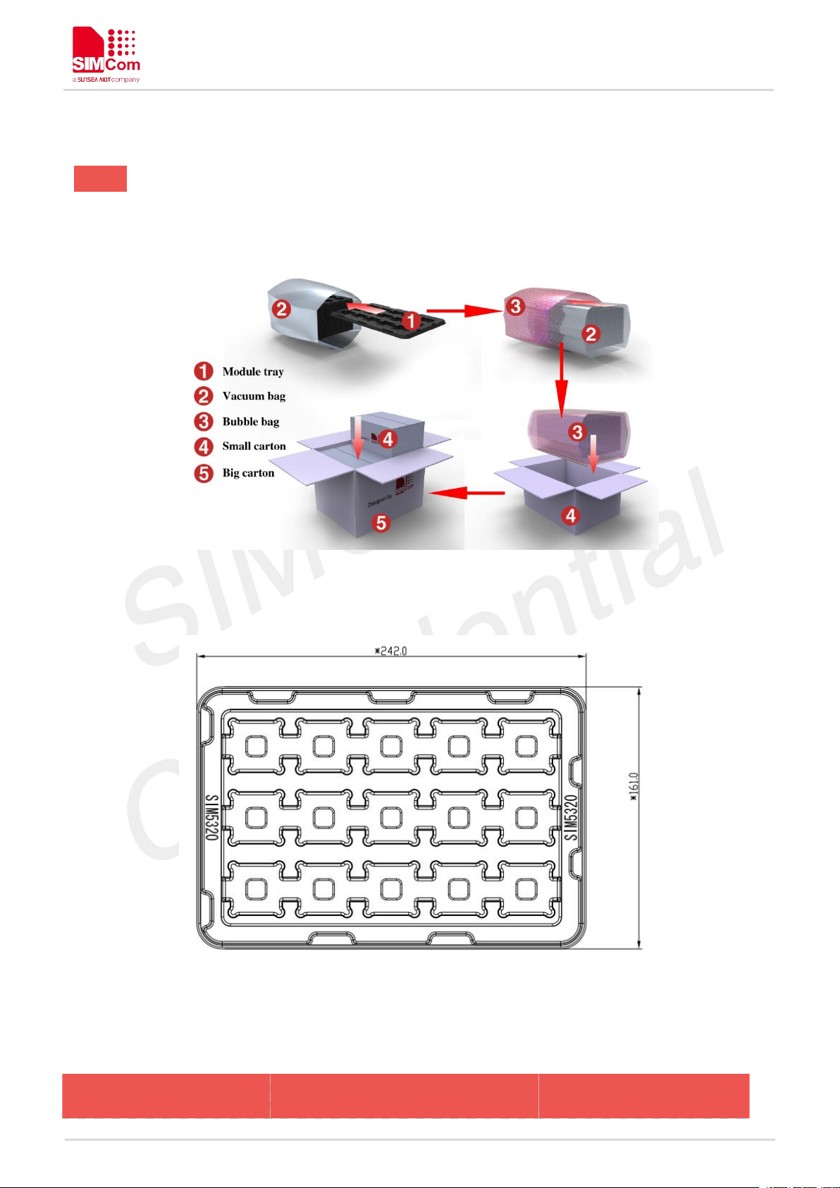
7 Packaging
Length(±3mm
)
Width(±3mm
)
Number
MODULE support tray packaging.
SIM7600G-H User manual
Figure 42 : Stencil Foil
Module tray drawing:
Figure 43: packaging diagram
Table 40: Tray size
www.simcom.com
Figure 44: Tray drawing
68/75
Page 69

242.0
161.0
15
Small carton drawing:
Length(±10mm
)
Width(±10mm
)
Height(±10mm
)
Number
270
180
120
15*20=300
SIM7600G-H User manual
Table 41: Small Carton size
Big carton drawing:
Figure 45: Small carton drawing
www.simcom.com
69/75
Page 70
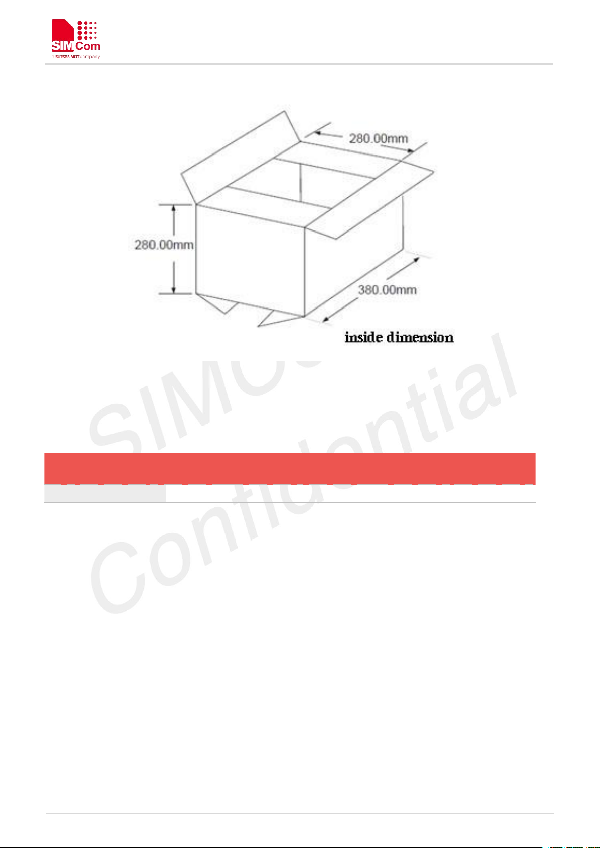
SIM7600G-H User manual
Length(±10mm
)
Width(±10mm
)
Height(±10mm
)
Number
380
280
280
300*4=1200
Table 42: Big Carton size
Figure 46: Big carton drawing
www.simcom.com
70/75
Page 71
SIM7600G-H User manual
LTE-FDD device category
(Downlink)
Max data rate(peak
)
Modulation type
Category 1
10Mbps
QPSK/16QAM/64QAM
Category 2
50Mbps
QPSK/16QAM/64QAM
Category 3
100Mbps
QPSK/16QAM/64QAM
Category 4
150Mbps
QPSK/16QAM/64QAM
LTE-FDD device category
(Uplink)
Max data rate(peak
)
Modulation type
Category 1
5Mbps
QPSK/16QAM
Category 2
25Mbps
QPSK/16QAM
Category 3
50Mbps
QPSK/16QAM
Category 4
50Mbps
QPSK/16QAM
NO.
Title
Description
[1]
SIM7500_SIM7600 Series_AT
Command Manual_V1.xx
AT Command Manual
[2]
ITU-T Draft new
recommendationV.25ter
Serial asynchronous automatic dialing and control
[3]
GSM 07.07
Digital cellular telecommunications (Phase 2+); AT command
set for GSM Mobile Equipment (ME)
[4]
GSM 07.10
Support GSM 07.10 multiplexing protocol
[5]
GSM 07.05
Digital cellular telecommunications (Phase 2+); Use of Data
Terminal Equipment – Data Circuit terminating Equipment
(DTE – DCE) interface for Short Message Service (SMS) and
Cell Broadcast Service (CBS)
8 Appendix
8.1 Coding Schemes and Maximum Net Data Rates over Air Interface
Table 43: Coding Schemes and Maximum Net Data Rates over Air Interface
8.2 Related Documents
Table 44: Related Documents
www.simcom.com
71/75
Page 72
SIM7600G-H User manual
[6]
GSM 11.14
Digital cellular telecommunications system (Phase 2+);
Specification of the SIM Application Toolkit for the Subscriber
Identity Module – Mobile Equipment (SIM – ME) interface
[7]
GSM 11.11
Digital cellular telecommunications system (Phase 2+);
Specification of the Subscriber Identity Module – Mobile
Equipment (SIM – ME) interface
[8]
GSM 03.38
Digital cellular telecommunications system (Phase 2+);
Alphabets and language-specific information
[9]
GSM 11.10
Digital cellular telecommunications system (Phase 2) ;
Mobile Station (MS) conformance specification ; Part 1:
Conformance specification
[10]
3GPP TS 51.010-1
Digital cellular telecommunications system (Release 5);
Mobile Station (MS) conformance specification
[11]
3GPP TS 34.124
Electromagnetic Compatibility (EMC) for mobile terminals and
ancillary equipment.
[12]
3GPP TS 34.121
Electromagnetic Compatibility (EMC) for mobile terminals and
ancillary equipment.
[13]
3GPP TS 34.123-1
Technical Specification Group Radio Access Network;
Terminal conformance specification; Radio transmission and
reception (FDD)
[14]
3GPP TS 34.123-3
User Equipment (UE) conformance specification; Part 3:
Abstract Test Suites.
[15]
Radio
ETSI EN 301 908-1 V13.1.1 (2019); ETSI EN 301 908-2
V13.1.1(2020);ETSI EN 301 908-13 V13.1.1(2019); ETSI EN303
413V1.1.1(2017)
[16]
EMC
ETSI EN 301 489-1 V2.2.3 (2019);EN 301 489-52 V1.1.0
(2016); ETSI EN301 489-19V2.1.1(2019)
[17]
Safety
EN 60950-1:2006+A11:2009+A1:2010+A12:2011+A2:2013
[18]
Health
EN 62311:2008
[19]
3GPP TS 51.010-1
Digital cellular telecommunications system (Release 5);
Mobile Station (MS) conformance specification
[20]
GCF-CC V3.23.1
Global Certification Forum - Certification Criteria
[21]
2002/95/EC
Directive of the European Parliament and of the Council of 27
January 2003 on the restriction of the use of certain
hazardous substances in electrical and electronic equipment
(RoHS)
[22]
Module
secondary-SMT-UGD-V1.xx
Module secondary SMT Guidelines
[23]
SIM7X00
Series_UART_Application
Note_V1.xx
This document describes how to use UART interface of
SIMCom modules.
[24]
SIM7100_SIM7500_SIM7600
Series_USB
AUDIO_Application
Note_V1.xx
USB AUDIO Application Note
[25]
SIM7X00
Series_GPS_Application
Note_V1.xx
GPS Application Note
[26]
Antenna design guidelines for
diversity receiver system
Antenna design guidelines for diversity receiver system
[27]
SIM7100_SIM7500_SIM7600_
Sleep Mode_Application
Note_V1.xx
Sleep Mode Application Note
[28]
7600CE-LAN-Reference
HSIC Application Note
www.simcom.com
72/75
Page 73

Design V1.0
[29]
SIM7600_Series_SGMII-Refer
ence_Design_V1.00
SGMII Reference Design
8.3 Terms and Abbreviations
Abbreviation
Description
ADC
Analog-to-Digital Converter
ARP
Antenna Reference Point
BER
Bit Error Rate
BTS
Base Transceiver Station
CS
Coding Scheme
CSD
Circuit Switched Data
CTS
Clear to Send
DAC
Digital-to-Analog Converter
DRX
Discontinuous Reception
DSP
Digital Signal Processor
DTE
Data Terminal Equipment (typically computer, terminal, printer)
DTR
Data Terminal Ready
DTX
Discontinuous Transmission
EFR
Enhanced Full Rate
EGSM
Enhanced GSM
EMC
Electromagnetic Compatibility
ESD
Electrostatic Discharge
ETS
European Telecommunication Standard
EVDO
Evolution Data Only
FCC
Federal Communications Commission (U.S.)
FD
SIM fix dialing phonebook
FDMA
Frequency Division Multiple Access
FR
Full Rate
GMSK
Gaussian Minimum Shift Keying
GNSS
Global Navigation Satellite System
GPRS
General Packet Radio Service
GPS
Global Positioning System
GSM
Global Standard for Mobile Communications
HR
Half Rate
HSPA
High Speed Packet Access
I2C
Inter-Integrated Circuit
IMEI
International Mobile Equipment Identity
Table 45: Terms and Abbreviations
SIM7600G-H User manual
www.simcom.com
73/75
Page 74
SIM7600G-H User manual
LTE
Long Term Evolution
MO
Mobile Originated
MS
Mobile Station (GSM engine), also referred to as TE
MT
Mobile Terminated
NMEA
National Marine Electronics Association
PAP
Password Authentication Protocol
PBCCH
Packet Switched Broadcast Control Channel
PCB
Printed Circuit Board
PCS
Personal Communication System, also referred to as GSM 1900
RF
Radio Frequency
RMS
Root Mean Square (value)
RTC
Real Time Clock
SIM
Subscriber Identification Module
SMS
Short Message Service
SPI
serial peripheral interface
SMPS
Switched-mode power supply
TDMA
Time Division Multiple Access
TE
Terminal Equipment, also referred to as DTE
TX
Transmit Direction
UART
Universal Asynchronous Receiver & Transmitter
VSWR
Voltage Standing Wave Ratio
SM
SIM phonebook
NC
Not connect
EDGE
Enhanced data rates for GSM evolution
HSDPA
High Speed Downlink Packet Access
HSUPA
High Speed Uplink Packet Access
ZIF
Zero intermediate frequency
WCDMA
Wideband Code Division Multiple Access
VCTCXO
Voltage control temperature-compensated crystal oscillator
USIM
Universal subscriber identity module
UMTS
Universal mobile telecommunications system
UART
Universal asynchronous receiver transmitter
www.simcom.com
74/75
Page 75
8.4 Safety Caution
Marks
Requirements
When in a hospital or other health care facility, observe the restrictions about the use
of mobiles. Switch the cellular terminal or mobile off, medical equipment may be
sensitive and not operate normally due to RF energy interference.
Switch off the cellular terminal or mobile before boarding an aircraft. Make sure it is
switched off. The operation of wireless appliances in an aircraft is forbidden to prevent
interference with communication systems. Forgetting to think much of these
instructions may impact the flight safety, or offend local legal action, or both.
Do not operate the cellular terminal or mobile in the presence of flammable gases or
fumes. Switch off the cellular terminal when you are near petrol stations, fuel depots,
chemical plants or where blasting operations are in progress. Operation of any
electrical equipment in potentially explosive atmospheres can constitute a safety
hazard.
Your cellular terminal or mobile receives and transmits radio frequency energy while
switched on. RF interference can occur if it is used close to TV sets, radios,
computers or other electric equipment.
Road safety comes first! Do not use a hand-held cellular terminal or mobile when
driving a vehicle, unless it is securely mounted in a holder for hands free operation.
Before making a call with a hand-held terminal or mobile, park the vehicle.
GSM cellular terminals or mobiles operate over radio frequency signals and cellular
networks and cannot be guaranteed to connect in all conditions, especially with a
mobile fee or an invalid SIM card. While you are in this condition and need emergent
help, please remember to use emergency calls. In order to make or receive calls, the
cellular terminal or mobile must be switched on and in a service area with adequate
cellular signal strength.
Some networks do not allow for emergency call if certain network services or phone
features are in use (e.g. lock functions, fixed dialing etc.). You may have to deactivate
those features before you can make an emergency call.
Also, some networks require that a valid SIM card be properly inserted in the cellular
terminal or mobile.
Table 46: Safety Caution
SIM7600G-H User manual
www.simcom.com
75/75
Page 76

Antenna requirements
1.
Antenna List:
Type: Dipole antenna with non-standard SMA connector(50ohm);
Model: MF25D
Antenna Gain:
Band 2:1.87dBi, Band 4:3.12dBi, Band 5:0.91dBi, Band 12:0.95dBi,
Band13:2.23dBi, Band 25:1.87dBi, Band 26:0.91dBi, Band 41:2.9dBi,
Band 66:3.12dBi
2.
The user must match the MF25D antenna with the non-standard SMA
connector and cannot change the antenna.
This device is intended only for OEM integrators under the following
conditions: (For module device use)
1)
The antenna must be installed such that 20 cm is maintained between the
antenna and users, and
2)
The transmitter module may not be co-located with any other transmitter or
antenna.
As long as 2 conditions above are met, further transmitter test will not be
required. However, the OEM integrator is still responsible for testing their endproduct for any additional compliance requirements required with this module
installed.
Radiation Exposure Statement
This equipment complies with IC radiation exposure limits set forth for an
uncontrolled environment. This equipment should be installed and operated with
minimum distance 20 cm between the radiator & your body.
Cet appareil est conçu uniquement pour les intégrateurs OEM dans les conditions
suivantes:
(Pour utilisation de dispositif module)
1) L'antenne doit être installée de telle sorte qu'une distance de 20 cm est respectée entre
l'antenne et les utilisateurs, et
2) Le module émetteur peut ne pas être coïmplanté avec un autre émetteur ou antenne.
Tant que les 2 conditions ci-dessus sont remplies, des essais supplémentaires sur l'émetteur
ne seront pas nécessaires. Toutefois, l'intégrateur OEM est toujours responsable des essais
sur son produit final pour toutes exigences de conformité supplémentaires requis pour ce
module installé.
Déclaration d'exposition aux radiations:
Cet équipement est conforme aux limites d'exposition aux rayonnements ISED établies pour un
environnement non contrôlé. Cet équipement doit être installé et utilisé avec un minimum de 20
cm de distance entre la source de rayonnement et votre corps.
Page 77

FCC Statement
This device complies with part 15 of the FCC Rules. Operation is subject to the
following two conditions:
(1)
This device may not cause harmful interference, and
(2)
this device must accept any interference received, including interference that
may cause undesired operation.
Any Changes or modifications not expressly approved by the party responsible for
compliance could void the user's authority to operate the equipment.
The modular can be installed or integrated in mobile or fix devices only. This
modular cannot be installed in any portable device.
FCC Radiation Exposure Statement
This modular complies with FCC RF radiation exposure limits set forth for an
uncontrolled environment. This transmitter must not be co-located or operating in
conjunction with any other antenna or transmitter. This modular must be installed and
operated with a minimum distance of 20 cm between the radiator and user body.
If the FCC identification number is not visible when the module is installed inside
another device, then the outside of the device into which the module is installed
must also display a label referring to the enclosed module. This
exterior label can use wording such as the following: “Contains Transmitter
Module FCC ID: 2AJYU-8PYA007 Or Contains FCC ID: 2AJYU-8PYA007”
When the module is installed inside another device, the user manual of the host
must contain below warning statements;
1.
This device complies with Part 15 of the FCC Rules. Operation is subject to the
following two conditions:
(1)
This device may not cause harmful interference.
(2)
This device must accept any interference received, including interference that
may cause undesired operation.
2.
Changes or modifications not expressly approved by the party responsible
for compliance could void the user's authority to operate the equipment.
The devices must be installed and used in strict accordance with the manufacturer's
instructions as described in the user documentation that comes with the product.
Any company of the host device which install this modular with limit modular
approval should perform the test of radiated emissionand spurious emission
according to FCC Part 22H and 24E, 47 CFR Part 2, 22H, 24(E), 27 and 47 CFR
Part 2, 22H, 24(E), 27, 90 requirement,Only if the test result comply with FCC Part
22H and 24E, 47 CFR Part 2, 22H, 24(E), 27 and 47 CFR Part 2,22H, 24(E), 27, 90
requirement, then the host can be sold legally.
Page 78

IC Warning
This device complies with Industry Canada licence-exempt RSS standard(s).
Operation is subject to the following two conditions:
(1)
This device may not cause interference, and
(2)
This device must accept any interference, including interference that may cause
undesired operation of the device.
The modular can be installed or integrated in mobile or fix devices only. This
modular cannot be installed in any portable device.
IC Radiation Exposure Statement
This modular complies with IC RF radiation exposure limits set forth for an
uncontrolled environment. This transmitter must not be co-located or operating in
conjunction with any other antenna or transmitter. This modular must be installed and
operated with a minimum distance of 20 cm between the radiator and user body.
For a host manufacture's using a certified modular, if (1) the module's IC
number is not visible
when installed in the host, or (2) if the host is marketed so that end users do not
have straightforward commonly used methods for access to remove the module so
that the IC number of the module is visible; then an additional permanent label
referring to the enclosed module: "Contains Transmitter Module IC: " 237618PYA008" or "Contains IC: 23761-8PYA008" must be used.
Le présent appareil est conforme aux CNR d'Industrie Canada applicables aux
appareils radio exempts de licence. L'exploitation est autorisée aux deux conditions
suivantes:
(1) l'appareil ne doit pas produire de brouillage, et
(2) l'utilisateur de l'appareil doit accepter tout brouillage radioélectrique subi, même si
le brouillage est susceptible d'en compromettre le fonctionnement
Le modular peut être installé ou intégré dans un mobile ou réparer une seule chose
Installation dans n’importe quel appareil portable.
Déclaration de rayonnement IC
Ce modular complies avec des radiations émettrices de rayonnement Environnement.
Ceci ne doit pas être co-localisé ou opérer avec des autres Ce modular doit être
installé et obtenu avec une distance minimale de 20 cm entre les radiateurs et le
corps de l’utilisateur.
Pour un hôte, on utilise un modular, si (1) le numéro de module est non visible
Quand on est installé dans le serveur, or (2) si le propriétaire est commercialisé
Straightforward commonly used for the access to remove travail so that the number
IC en vue Le module est visible; Ensuite, le label permanent a été attribué au module:
"Contient le Module IC:" 23761-8PYA008" ou "contenu IC: 23761-8PYA008" doit" be
use
 Loading...