

Page 1

SIM300
HARDWARE
SPECIFICATION
SIMCOM Ltd,.
th
Jul 2006
27
Page 2

SIM300 Hardware Interface Description
Confidential
SIMCOM
Document Name:
Version:
Date:
Doc Id:
Status:
General Notes
Simcom offers this information as a service to its customers, to support application and
engineering efforts that use the products designed by Simcom. The information provided is based
upon requirements specifically provided to Simcom by the customers. Simcom has not undertaken
any independent search for additional relevant information, including any information that may be
in the customer’s possession. Furthermore, system validation of this designed by Simcom within a
larger electronic system remains the responsibility of the customer or the customer’s system
integrator. All specifications supplied herein are subject to change.
Copyright
This document contains proprietary technical information which is the property of SIMCOM
Limited., copying of this document and giving it to others and the using or communication of the
contents thereof, are forbidden without express authority. Offenders are liable to the payment of
damages. All rights reserved in the event of grant of a patent or the registration of a utility model
or design. All specification supplied herein are subject to change without notice at any time.
SIM300 Hardware Interface Description
03.02
2006-06-27
SIM300_HD_V3.02
Release
Copyright © SIMCOM Limited. 2006
SIM300_HD_V3.02 Page 2 of 56
Page 3

SIM300 Hardware Interface Description
Confidential
SIMCOM
Contents
Contents ............................................................................................................................................3
Version History ................................................................................................................................. 6
1 Introduction.................................................................................................................................... 7
1.1 Related documents .............................................................................................................. 7
1.2 Terms and abbreviations......................................................................................................8
2 Product concept............................................................................................................................ 11
2.1 SIM300 key features at a glance .......................................................................................12
3 Application Interface....................................................................................................................14
3.1 SIM300 Pin description.....................................................................................................14
3.2 Operating modes ...............................................................................................................16
3.3 Power supply.....................................................................................................................17
3.3.1 Power supply pins on the board-to-board connector.............................................. 18
3.3.2 Minimizing power losses .......................................................................................18
3.3.3 Monitoring power supply.......................................................................................19
3.4 Power up and power down scenarios ................................................................................ 19
3.4.1 Turn on SIM300 .....................................................................................................19
3.4.2 Turn off SIM300 ....................................................................................................21
3.4.3 Restart SIM300 using the PWRKEY pin ............................................................... 23
3.5 Power saving .....................................................................................................................23
3.5.1 Minimum functionality mode.................................................................................24
3.5.2 Sleep mode (Slow Clocking mode)........................................................................24
3.5.3 Wake up SIM300 from SLEEP mode .................................................................... 24
3.6 Summary of state transitions (except SLEEP mode) ........................................................25
3.7 RTC backup.......................................................................................................................25
3.8 Serial interfaces................................................................................................................. 28
3.8.1 Function of Serial Port 1 & 2 supporting...............................................................29
3.8.2 Software upgrade and Software debug...................................................................31
3.9 Audio interfaces ................................................................................................................ 32
3.9.1 Speaker interface configuration .............................................................................33
3.9.2 Microphone interfaces configuration .....................................................................34
3.9.3 Earphone interface configuration...........................................................................34
3.9.4 Referenced Electronic Characteristic.....................................................................35
3.10 Buzzer .............................................................................................................................35
3.11 SIM card interface...........................................................................................................36
3.11.1 SIM card application............................................................................................36
3.11.2 Design considerations for SIM card holder..........................................................38
3.12 LCD interface..................................................................................................................40
3.13 ADC ................................................................................................................................40
3.14 Behaviors of the /RING line (Serial port1 interface only) ..............................................41
3.15 Network status indication LED lamp .............................................................................. 42
3.16 General Purpose Input Output (GPIO)............................................................................43
SIM300_HD_V3.02 Page 3 of 56
Page 4

SIM300 Hardware Interface Description
Confidential
SIMCOM
4 Antenna interface .........................................................................................................................44
4.1 Antenna installation...........................................................................................................44
4.1.1 Antenna connector .................................................................................................44
4.1.2 Antenna pad ...........................................................................................................44
4.2 Module RF output power .................................................................................................. 44
4.3 Module RF receive sensitivity...........................................................................................45
4.4 Module receive/transmit frequency...................................................................................45
4.5 Antenna gain .....................................................................................................................45
5 Electrical, reliability and radio characteristics .............................................................................46
5.1 Absolute maximum ratings ...............................................................................................46
5.2 Operating temperatures ..................................................................................................... 46
5.3 Power supply ratings .........................................................................................................47
5.4 Current Consumption........................................................................................................48
5.5 Electro-Static discharge.....................................................................................................49
6 Mechanics ....................................................................................................................................50
6.1 Mechanical dimensions of SIM300...................................................................................50
6.2 Mounting SIM300 onto the application platform..............................................................51
6.3 Board-to-board connector .................................................................................................51
6.3.1 Mechanical dimensions of the ENTERY 1008-G60N-01R ...................................51
6.4 RF Adapter cabling ...........................................................................................................53
6.5 Top view of the SIM300....................................................................................................55
6.6 PIN assignment of board-to-board connector of SIM300.................................................56
Table index:
TABLE 1: RELATED DOCUMENTS .....................................................................................................7
TABLE 2: TERMS AND ABBREVIATIONS .........................................................................................8
TABLE 3: SIM300 KEY FEATURES.................................................................................................... 12
TABLE 4: CODING SCHEMES AND MAXIMUM NET DATA RATES OVER AIR INTERFACE .. 13
TABLE 5: BOARD-TO-BOARD CONNECTOR PIN DESCRIPTION ...............................................14
TABLE 6: OVERVIEW OF OPERATING MODES..............................................................................16
TABLE 7: AT COMMANDS USED IN ALARM MODE ..................................................................... 20
TABLE 8: SUMMARY OF STATE TRANSITIONS............................................................................. 25
TABLE 9: LOGIC LEVELS OF SERIAL PORTS PINS ....................................................................... 29
TABLE 10: AUDIO INTERFACE SIGNAL.......................................................................................... 32
TABLE 11: MIC INPUT DC CHARACTERISTICS.............................................................................35
TABLE 12: AUDIO OUTPUT CHARACTERISTICS.......................................................................... 35
TABLE 13: BUZZER OUTPUT DC CHARACTERISTICS.................................................................35
TABLE 14: SIGNAL OF SIM INTERFACE (BOARD-TO-BOARD CONNECTOR)......................... 37
TABLE 15: PIN DESCRIPTION (AMPHENOL SIM CARD HOLDER) ............................................39
TABLE 16: PIN DESCRIPTION (MOLEX SIM CARD HOLDER) ....................................................40
TABLE 17: PIN DEFINE OF LCD INTERFACE .................................................................................40
TABLE 18: ADC PIN OF SIM300......................................................................................................... 41
TABLE 19: BEHAVIOURS OF THE /RING LINE...............................................................................41
TABLE 20: WORKING STATE OF NETWORK STATUS INDICATION LED PIN...........................42
SIM300_HD_V3.02 Page 4 of 56
Page 5

SIM300 Hardware Interface Description
Confidential
TABLE 21: GPIO PINS OF SIM300 ..................................................................................................... 43
TABLE 22: SIM300 RF OUTPUT POWER .......................................................................................... 44
TABLE 23: SIM300 RF RECEIVE SENSITIVITY ..............................................................................45
TABLE 24: SIM300 RECEIVE/TRANSMIT FREQUENCY ...............................................................45
TABLE 25: ANTENNA GAIN............................................................................................................... 45
TABLE 26: ABSOLUTE MAXIMUM RATINGS................................................................................. 46
TABLE 27: SIM300 OPERATING TEMPERATURE ...........................................................................46
TABLE 28: SIM300 POWER SUPPLY RATINGS ............................................................................... 47
TABLE 29: SIM300 CURRENT CONSUMPTION ..............................................................................48
TABLE 30: THE ESD ENDURE STATUE MEASURED TABLE (TEMPERATURE: 25℃,
HUMIDITY:45% ) .........................................................................................................................49
TABLE 31: CONNECTION DIAGRAMS ............................................................................................56
SIMCOM
Figure Index
FIGURE 1: VBAT INPUT......................................................................................................................18
FIGURE 2: VBAT RIPPLE WAVE AT THE MAXIMUM POWER TRANSMIT PHASE................... 18
FIGURE 3: TIMING OF TURN ON SYSTEM .....................................................................................19
FIGURE 4: TIMING OF TURN OFF SYSTEM ...................................................................................21
FIGURE 5: TIMING OF RESTART SYSTEM .....................................................................................23
FIGURE 6: RTC SUPPLY FROM NON-CHARGEABLE BATTERY .................................................25
FIGURE 7: RTC SUPPLY FROM RECHARGEABLE BATTERY ......................................................26
FIGURE 8: RTC SUPPLY FROM CAPACITOR ..................................................................................26
FIGURE 9: PANASONIC EECEMOE204A CHARGE CHARACTERISTIC......................................27
FIGURE 10: MAXELL TC614 CHARGE CHARACTERISTIC..........................................................27
FIGURE 11: SEIKO TS621 CHARGE CHARACTERISTIC ............................................................... 28
FIGURE 12: INTERFACE OF SERIAL PORTS................................................................................... 29
FIGURE 13: INTERFACE OF SOFTWARE UPGRADE .....................................................................31
FIGURE 14: INTERFACE OF SOFTWARE DEBUG ..........................................................................31
FIGURE 15: SPEAKER INTERFACE CONFIGURATION ................................................................. 33
FIGURE 16: SPEAKER INTERFACE WITH AMPLIFIER CONFIGURATION ................................33
FIGURE 17: MICROPHONE INTERFACE CONFIGURATION......................................................... 34
FIGURE 18: EARPHONE INTERFACE CONFIGURATION.............................................................. 34
FIGURE 19: REFERENCE CIRCUIT FOR BUZZER.......................................................................... 36
FIGURE 20: SIM INTERFACE REFERENCE CIRCUIT WITH 8 PINS SIM CARD ........................37
FIGURE 21: SIM INTERFACE REFERENCE CIRCUIT WITH 6 PINS SIM CARD ........................38
FIGURE 22: AMPHENOL C707 10M006 512 2 SIM CARD HOLDER.............................................. 38
FIGURE 23: MOLEX 91228 SIM CARD HOLDER ............................................................................39
FIGURE 24: SIM300 SERVICES AS RECEIVER................................................................................ 41
FIGURE 25: SIM300 SERVICES AS CALLER.................................................................................... 42
FIGURE 26: REFERENCE CIRCUIT FOR NETWORK STATUS LED..............................................42
FIGURE 27: MECHANICAL DIMENSIONS OF SIM300(UNIT: MM) ........................................50
FIGURE 28: ENTERY 1008-G60N-01R BOARD-TO-BOARD CONNECTOR PIN SIDE ................51
FIGURE 29: ENTERY BOARD TO BOARD CONNECTOR PHYSICAL PHOTO............................ 52
FIGURE 30: MM9329-2700B................................................................................................................ 53
FIGURE 31: RF CONNECTOR MXTK................................................................................................ 54
SIM300_HD_V3.02 Page 5 of 56
Page 6

SIM300 Hardware Interface Description
Confidential
SIMCOM
Version History
Data Version Description of change Author
2005-04-13 01.00 Origin anthony
2005-06-29 01.01 Modify the RESET pin DC characteristics etc. anthony
2005-08-02 01.02 Modify the ESD characteristics etc. anthony
2005-08-23 01.03 Delete reset part, update Mechanical dimensions sleep
mode and board-to-board connector description
2005-11-02 01.04 Add the SIM300 current consumption, modify the Buzzer
pin
2005-11-22 01.05 Add the restart timing figure anthony
2005-12-27 01.06 Add the Software upgrade, the auto-baud and the over
temperature power off.
Modify the sleep mode control and the SIM card detection.
2006-02-22 01.07 Modify the figure 3,4,5,20,28 and add the figure 14 anthony
2006-03-16 02.01 Modify for SIM300_V7.02
Add support GPRS class 8, Modify the VDD_EXT level,
“RDY” out by set fixed baudrate, timing of the turn on
system
2006-04-04 02.02 Modify the function of GPIO5 and BUZZER pins, the 10K
resistance integrated in the VRTC pin. Add the description
of the Autobauding function.
2006-05-09 02.03 Update Temperature range.
Modify the mechanical dimensions of SIM300.
Delete the description of MOLEX connector.
Modify the figure of the SIM reference circuit.
anthony
anthony
anthony
anthony
anthony
anthony
2006-6-10 03.01 Update the figure of SIM card holder anthony
2006-7-27 03.02 Add the note about the VRTC pin.
Add the note about the configuration be set and saved as
the fix baud rate.
SIM300_HD_V3.02 Page 6 of 56
anthony
Page 7
SIM300 Hardware Interface Description
Confidential
SIMCOM
1 Introduction
This document describes the hardware interface of the SIMCOM SIM300 module that connects to
the specific application and the air interface. As SIM300 can be integrated with a wide range of
applications, all functional components of SIM300 are described in great detail.
This document can help you quickly understand SIM300 interface specifications, electrical and
mechanical details. With the help of this document and other SIM300 application notes, user guide,
you can use SIM300 module to design and set-up mobile applications quickly.
1.1 Related documents
Table 1: Related documents
SN Document name Remark
[1] SIM300_ATC_V01.05 SIM300_ATC_V01.05
[2] ITU-T Draft new
recommendation
V.25ter:
[3] GSM 07.07: Digital cellular telecommunications (Phase 2+); AT command
[4] GSM 07.10:
[5] GSM 07.05: Digital cellular telecommunications (Phase 2+); Use of Data
[6] GSM 11.14: Digital cellular telecommunications system (Phase 2+);
[7] GSM 11.11: Digital cellular telecommunications system (Phase 2+);
Serial asynchronous automatic dialing and control
set for GSM Mobile Equipment (ME)
Support GSM 07.10 multiplexing protocol
Terminal Equipment – Data Circuit terminating Equipment
(DTE – DCE) interface for Short Message Service (SMS) and
Cell Broadcast Service (CBS)
Specification of the SIM Application Toolkit for the Subscriber
Identity Module – Mobile Equipment (SIM – ME) interface
Specification of the Subscriber Identity Module – Mobile
Equipment (SIM – ME) interface
[8] GSM 03.38: Digital cellular telecommunications system (Phase 2+);
Alphabets and language-specific information
[9] GSM 11.10 Digital cellular telecommunications system (Phase 2) ;
Mobile Station (MS) conformance specification; Part 1:
Conformance specification
SIM300_HD_V3.02 Page 7 of 56
Page 8

SIM300 Hardware Interface Description
Confidential
SIMCOM
1.2 Terms and abbreviations
Table 2: Terms and abbreviations
Abbreviation Description
ADC Analog-to-Digital Converter
ARP Antenna Reference Point
ASIC Application Specific Integrated Circuit
BER Bit Error Rate
BTS Base Transceiver Station
CHAP Challenge Handshake Authentication Protocol
CS Coding Scheme
CSD Circuit Switched Data
CTS Clear to Send
DAC Digital-to-Analog Converter
DRX Discontinuous Reception
DSP Digital Signal Processor
DTE Data Terminal Equipment (typically computer, terminal, printer)
DTR Data Terminal Ready
DTX Discontinuous Transmission
EFR Enhanced Full Rate
EGSM Enhanced GSM
EMC Electromagnetic Compatibility
ESD Electrostatic Discharge
ETS European Telecommunication Standard
FCC Federal Communications Commission (U.S.)
FDMA Frequency Division Multiple Access
FR Full Rate
GMSK Gaussian Minimum Shift Keying
GPRS General Packet Radio Service
GSM Global Standard for Mobile Communications
HR Half Rate
I/O Input/Output
IC Integrated Circuit
IMEI International Mobile Equipment Identity
Inorm Normal Current
Imax Maximum Load Current
kbps Kilo bits per second
LED Light Emitting Diode
SIM300_HD_V3.02 Page 8 of 56
Page 9

SIM300 Hardware Interface Description
Confidential
SIMCOM
Abbreviation Description
Li-Ion Lithium-Ion
MO Mobile Originated
MS Mobile Station (GSM engine), also referred to as TE
MT Mobile Terminated
PAP Password Authentication Protocol
PBCCH Packet Switched Broadcast Control Channel
PCB Printed Circuit Board
PCS Personal Communication System, also referred to as GSM 1900
PDU Protocol Data Unit
PPP Point-to-point protocol
RF Radio Frequency
RMS Root Mean Square (value)
RTC Real Time Clock
Rx Receive Direction
SIM Subscriber Identification Module
SMS Short Message Service
TDMA Time Division Multiple Access
TE Terminal Equipment, also referred to as DTE
TX Transmit Direction
UART Universal Asynchronous Receiver & Transmitter
URC Unsolicited Result Code
USSD Unstructured Supplementary Service Data
VSWR Voltage Standing Wave Ratio
Vmax Maximum Voltage Value
Vnorm Normal Voltage Value
Vmin Minimum Voltage Value
VIHmax Maximum Input High Level Voltage Value
VIHmin Minimum Input High Level Voltage Value
VILmax Maximum Input Low Level Voltage Value
VILmin Minimum Input Low Level Voltage Value
VImax Absolute Maximum Input Voltage Value
VImin Absolute Minimum Input Voltage Value
VOHmax Maximum Output High Level Voltage Value
VOHmin Minimum Output High Level Voltage Value
VOLmax Maximum Output Low Level Voltage Value
VOLmin Minimum Output Low Level Voltage Value
Phonebook abbreviations
SIM300_HD_V3.02 Page 9 of 56
Page 10

SIM300 Hardware Interface Description
Confidential
SIMCOM
Abbreviation Description
FD SIM fix dialing phonebook
LD SIM last dialing phonebook (list of numbers most recently dialed)
MC Mobile Equipment list of unanswered MT calls (missed calls)
ON
SIM (or ME) own numbers (MSISDNs) list
RC Mobile Equipment list of received calls
SM SIM phonebook
NC Not connect
SIM300_HD_V3.02 Page 10 of 56
Page 11

SIM300 Hardware Interface Description
Confidential
SIMCOM
2 Product concept
Designed for global market, SIM300 is a Tri-band GSM/GPRS engine that works on frequencies
EGSM 900 MHz, DCS 1800 MHz and PCS1900 MHz. SIM300 provides GPRS multi-slot class
10/ class 8 (optional) capability and support the GPRS coding schemes CS-1, CS-2, CS-3 and
CS-4.
With a tiny configuration of 40mm x 33mm x 2.85 mm , SIM300 can fit almost all the space
requirement in your application, such as Smart phone, PDA phone and other mobile device.
The physical interface to the mobile application is made through a 60 pins board-to-board
connector, which provides all hardware interfaces between the module and customers’ boards
except the RF antenna interface.
z The keypad and SPI LCD interface will give you the flexibility to develop customized
applications.
z Two serial ports can help you easily develop your applications.
z Two audio channels include two microphones inputs and two speaker outputs. This can
be easily configured by AT command.
SIM300 provide RF antenna interface with two alternatives: antenna connector and antenna pad.
The antenna connector is MURATA MM9329-2700. And customer’s antenna can be soldered to
the antenna pad.
The SIM300 is designed with power saving technique, the current consumption to as low as
2.5mA in SLEEP mode.
The SIM300 is integrated with the TCP/IP protocol,Extended TCP/IP AT commands are
developed for customers to use the TCP/IP protocol easily, which is very useful for those data
transfer applications.
SIM300_HD_V3.02 Page 11 of 56
Page 12

SIM300 Hardware Interface Description
Confidential
SIMCOM
2.1 SIM300 key features at a glance
Table 3: SIM300 key features
Feature Implementation
Power supply Single supply voltage 3.4V – 4.5V
Power saving Typical power consumption in SLEEP mode to 2.5mA
Frequency bands
GSM class Small MS
Transmit power z Class 4 (2W) at EGSM900
GPRS connectivity
Temperature range
DATA GPRS:
CSD:
z SIM300 Tri-band: EGSM 900, DCS 1800, PCS 1900. The band
can be set by AT COMMAND, and default band is EGSM 900
and DCS 1800.
z Compliant to GSM Phase 2/2+
z Class 1 (1W) at DCS1800 and PCS 1900
z GPRS multi-slot class 10 (default)
z GPRS multi-slot class 8 (option)
z GPRS mobile station class B
z Normal operation: -20°C to +55°C
z Restricted operation: -30°C to -20°C and +55°C to +80°C
z Storage temperature -40°C to +85°C
z GPRS data downlink transfer: max. 85.6 kbps
z GPRS data uplink transfer: max. 42.8 kbps
z Coding scheme: CS-1, CS-2, CS-3 and CS-4
z SIM300 supports the protocols PAP (Password Authentication
Protocol) usually used for PPP connections.
z The SIM300 integrates the TCP/IP protocol.
z Support Packet Switched Broadcast Control Channel (PBCCH)
z CSD transmission rates: 2.4, 4.8, 9.6, 14.4 kbps, non-transparent
z Unstructured Supplementary Services Data (USSD) support
SMS z MT, MO, CB, Text and PDU mode
z SMS storage: SIM card
z Support transmission of SMS alternatively over CSD or GPRS.
User can choose preferred mode.
FAX Group 3 Class 1
SIM interface Supported SIM card: 1.8V ,3V
External antenna Connected via 50 Ohm antenna connector or antenna pad
Audio features Speech codec modes:
z Half Rate (ETS 06.20)
z Full Rate (ETS 06.10)
z Enhanced Full Rate (ETS 06.50 / 06.60 / 06.80)
z Echo suppression
Two serial interfaces z Serial Port 1 Seven lines on Serial Port Interface
SIM300_HD_V3.02 Page 12 of 56
Page 13
SIM300 Hardware Interface Description
Confidential
SIMCOM
z Serial Port 1 can be used for CSD FAX, GPRS service and send
AT command of controlling module.
z Serial Port 1 can use multiplexing function, but you can not use
the Serial Port 2 at the same time;
z Autobauding supports baud rate from 1200 bps to 115200bps.
z Serial port 2 Two lines on Serial Port Interface /TXD and /RXD
z Serial Port 2 only used for transmitting AT command.
Phonebook management Supported phonebook types: SM, FD, LD, RC, ON, MC.
SIM Application Toolkit Supports SAT class 3, GSM 11.14 Release 98
Real time clock Implemented
Timer function Programmable via AT command
Physical characteristics Size: 40±0.15 x 33±0.15 x 3.3±0.3 mm (including application
connector)
40±0.15 x 33±0.15 x 2.85±0.3 mm (excluding application connector)
Weight: 8g
Firmware upgrade Firmware upgradeable over serial interface
Table 4: Coding schemes and maximum net data rates over air interface
Coding scheme 1 Timeslot 2 Timeslot 4 Timeslot
CS-1: 9.05kbps 18.1kbps 36.2kbps
CS-2: 13.4kbps 26.8kbps 53.6kbps
CS-3: 15.6kbps 31.2kbps 62.4kbps
CS-4: 21.4kbps 42.8kbps 85.6kbps
SIM300_HD_V3.02 Page 13 of 56
Page 14

SIM300 Hardware Interface Description
Confidential
SIMCOM
3 Application Interface
All hardware interfaces except RF interface that connects SIM300 to the customers’ cellular
application platform is through a 60-pin 0.5mm pitch board-to-board connector. Sub-interfaces
included in this board-to-board connector are described in detail in following chapters:
z Power supply (see Chapters 3.3)
z Dual serial interface (
z Two analog audio interfaces (
z SIM interface (
Electrical and mechanical characteristics of the board-to-board connector are specified in Chapter
6. There we also order information for mating connectors.
see Chapter 3.8)
see Chapter 3.9)
see Chapter 3.11)
3.1 SIM300 Pin description
Table 5: Board-to-Board Connector pin description
Power Supply
PIN NAME I/O DESCRIPTION DC CHARACTERISTICS
VBAT Eight BAT pins of the board-to-board
connector are dedicated to connect
the supply voltage. The power supply
of SIM300 has to be a single voltage
source of VBAT= 3.4V...4.5V. It must
be able to provide sufficient current
in a transmit burst which typically
rises to 2A.mostly, these 8 pins are
voltage input
VRTC I/O Current input for RTC when the
battery is not supplied for the system.
Current output for backup battery
when the main battery is present and
the backup battery in low voltage
state.
Vmax= 4.5V
Vmin=3.4V
Vnorm=4.0V
Vmax=2.0V
Vmin=1.2V
Vnorm=1.8V
Inorm= 20uA
VDD_EXT O Supply 2.93V voltage for external
circuit. By measure this pin, user
can judge the system is on or off.
When the voltage is low, the system
is off. Otherwise, the system is on.
GND Digital ground
SIM300_HD_V3.02 Page 14 of 56
Vmax=3.0V
Vmin=2.75V
Vnorm=2.93V
Imax=60mA
Page 15

SIM300 Hardware Interface Description
Confidential
SIMCOM
Power on or power off
PIN NAME I/O DESCRIPTION DC CHARACTERISTICS
PWRKEY I Voltage input for power on key.
PWRKEY get a low level Voltage for
user to power on or power off the
VILmax=0.3*VBAT
VIHmin=0.7*VBAT
VImax=VBAT
system, The user should keep
pressing the key for a moment when
power on or power off the system.
Because the system need margin time
assert the software.
Audio interfaces
PIN NAME I/O DESCRIPTION DC CHARACTERISTICS
MIC1P
MIC1N
MIC2P
MIC2N
SPK1P
SPK1N
SPK2P
SPK2N
I Positive and negative voice-band
input
I Auxiliary positive and negative
voice-band input
O Positive and negative voice-band
output
O Auxiliary positive and negative
voice-band output
Audio DC Characteristics
refer to chapter 3.9.4
Buzzer/GPIO8 O Buzzer Output
AGND Analog ground
General purpose input/output
PIN NAME I/O DESCRIPTION DC CHARACTERISTICS
KBC0~KBC4 O
KBR0~KBR4 I
SPI_DATA I/O
SPI_CLK O
SPI_CS O
SPI_D/C O
SPI_RST O
Network LED
O
The GPO can be configured by AT
command for outputting high or low
level voltage. All of the GPOs are
initial low without any setting from
AT command.
VILmin=0V
VILmax=0.3 *VDD_EXT
VIHmin=0.7*VDD_EXT
VIHmax= VDD_EXT+0.3
VOLmin=GND
VOLmax=0.2V
VOHmin= VDD_EXT-0.2
VOHmax= VDD_EXT
GPIO5 I/O Normal Input/Output Port
Serial 1 interface
PIN NAME I/O DESCRIPTION DC CHARACTERISTICS
DTR I Data Terminal Ready
RXD I Receive Data
TXD O Transmit Data
RTS I Request to Send
VILmin=0V
VILmax=0.3*VDD_EXT
VIHmin=0.7*VDD_EXT
VIHmax= VDD_EXT+0.3
VOLmin=GND
CTS O Clear to Send
SIM300_HD_V3.02 Page 15 of 56
Page 16

SIM300 Hardware Interface Description
Confidential
SIMCOM
RI O Ring Indicator
DCD
O Data Carrier detection
Serial 2 interface
DBGTX O
Serial interface for debugging and
VOLmax=0.2V
VOHmin= VDD_EXT-0.2
VOHmax= VDD_EXT
communication
DBGRX I
SIM interface
PIN NAME I/O DESCRIPTION DC CHARACTERISTICS
SIM_VDD O Voltage Supply for SIM card The voltage can be select
by software either 1.8v or
3V
SIM_I/O I/O SIM Data Output
SIM_CLK O SIM Clock
SIM_PRESENCE I SIM Card Detection
SIM_RST O SIM Reset
VILmin=0V
VILmax=0.3*SIM_VDD
VIHmin=0.7*SIM_VDD
VIHmax= SIM_VDD+0.3
VOLmin=GND
VOLmax=0.2V
VOHmin= SIM_VDD-0.2
VOHmax= SIM_VDD
AUXADC
PIN NAME I/O DESCRIPTION DC CHARACTERISTICS
ADC0 I General purpose analog to digital
converter.
Input voltage value scope
0V to 2.4V
3.2 Operating modes
The following table summarizes the various operating modes, each operating modes is referred to
in the following chapters.
Table 6: Overview of operating modes
Mode Function
Normal operation GSM/GPRS
SLEEP
Module will automatically go into SLEEP mode if DTR is set
to high level and there is no on air or audio activity is required
and no hardware interrupt (such as GPIO interrupt or data on
serial port).
In this case, the current consumption of module will reduce to
the minimal level.
During sleep mode, the module can still receive paging
message and SMS from the system normally.
SIM300_HD_V3.02 Page 16 of 56
Page 17

SIM300 Hardware Interface Description
Confidential
SIMCOM
GSM IDLE Software is active. Module has registered to the GSM network,
and the module is ready to send and receive.
GSM TALK CSD connection is going on between two subscribers. In this
case, the power consumption depends on network settings such
as DTX off/on, FR/EFR/HR, hopping sequences, antenna.
GPRS IDLE Module is ready for GPRS data transfer, but no data is
currently sent or received. In this case, power consumption
depends on network settings and GPRS configuration (e.g.
multi-slot settings).
GPRS DATA There is GPRS data in transfer (PPP or TCP or UDP). In this
case, power consumption is related with network settings (e.g.
power control level), uplink / downlink data rates and GPRS
configuration (e.g. used multi-slot settings).
POWER DOWN Normal shutdown by sending the “AT+CPOWD=1” command or using the
PERKEY. The power management ASIC disconnects the power supply from the
base band part of the module, only the power supply for the RTC is remained.
Software is not active. The serial interfaces are not accessible. Operating voltage
(connected to VBAT) remains applied.
Minimum
functionality
mode (without
remove power
supply)
Use the “AT+CFUN” command can set the module to a minimum functionality
mode without remove the power supply. In this case, the RF part of the module
will not work or the SIM card is not accessible, or RF part and SIM card be
closed all, the serial interfaces is still accessible. The power consumption in this
case is very low.
Alarm mode RTC alert function launches this restricted operation while the module is in
POWER DOWN mode. SIM300 will not be registered to GSM network and
only parts of AT commands can be available.
3.3 Power supply
The power supply of SIM300 is from a single voltage source of VBAT= 3.4V...4.5V. In some
case, the ripple in a transmit burst may cause voltage drops when current consumption rises to
typical peaks of 2A, So the power supply must be able to provide sufficient current up to 2A.
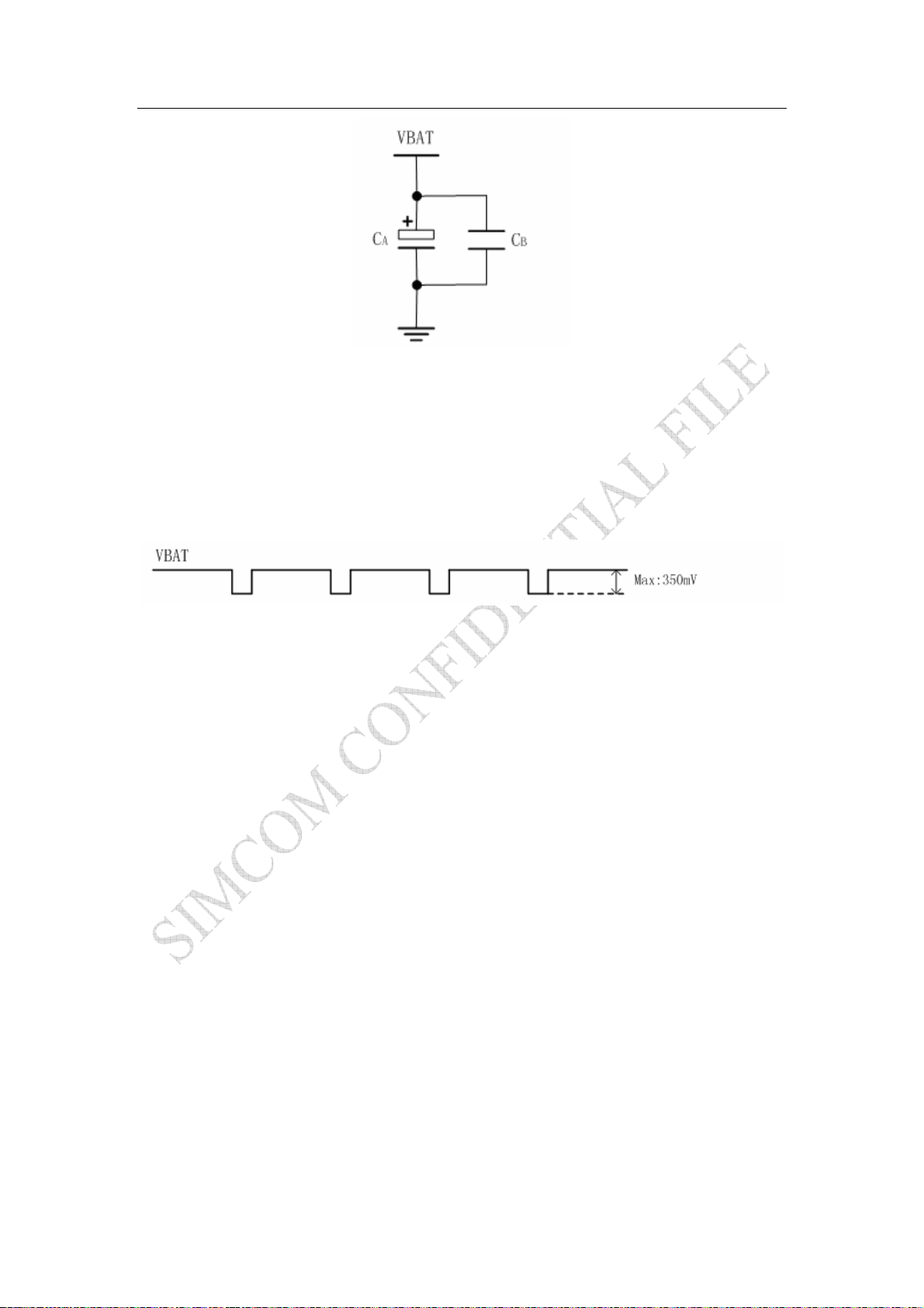
For the VBAT input, a local bypass capacitor is recommended. A capacitor (about 100µF, low
ESR) is recommended. Multi-layer ceramic chip (MLCC) capacitors can provide the best
combination of low ESR and small size but may not be cost effective. A lower cost choice may be
a 100 µF tantalum capacitor (low ESR) with a small (1 µF to 10µF) ceramic in parallel, which is
illustrated as following figure. And the capacitors should put as closer as possible to the SIM300
VBAT pins. The following figure is the recommended circuit.
SIM300_HD_V3.02 Page 17 of 56
Page 18
SIM300 Hardware Interface Description
Confidential
SIMCOM
Figure 1: VBAT input
The following figure is the VBAT voltage ripple wave at the maximum power transmit phase,
the test condition is VBAT=4.0V, VBAT maximum output current =2A, C
capacitor (ESR=0.7Ω) and C
=4.7µF. B
B
=100 µF tantalum
A
Figure2: VBAT ripple wave at the maximum power transmit phase
3.3.1 Power supply pins on the board-to-board connector
Eight VBAT pins of the board-to-board connector are dedicated to connect the supply voltage;
four GND pins are recommended for grounding. BACKUP can be used to back up the RTC.
3.3.2 Minimizing power losses
Please pay special attention to the supply power when you are designing your applications. Please
make sure that the input voltage will never drops below 3.4V even in a transmit burst during
which the current consumption may rise up to 2A. If the power voltage drops below 3.4V, the
module may be switched off. Using the board-to-board connector will be the best way to reduce
the voltage drops. You should also take the resistance of the power supply lines on the host board
or of battery pack into account.
SIM300_HD_V3.02 Page 18 of 56
Page 19

SIM300 Hardware Interface Description
Confidential
3.3.3 Monitoring power supply
To monitor the supply voltage, you can use the “AT+CBC” command which include three
parameters: voltage percent and voltage value (in mV). It returns the battery voltage 1-100 percent
of capacity and actual value measured at VBAT and GND.
The voltage is continuously measured at intervals depending on the operating mode. The
displayed voltage (in mV) is averaged over the last measuring period before the AT+CBC
command was executed.
For details please refer to document [1]
SIMCOM
3.4 Power up and power down scenarios
3.4.1 Turn on SIM300
SIM300 can be turned on by various ways, which are described in following chapters:
z Via PWRKEY pin: starts normal operating mode (see chapter 3.4.1.1);
z Via RTC interrupt: starts ALARM modes (see chapter 3.4.1.2)
Note: The AT command must be set after the SIM300 is power on and Unsolicited Result
Code “RDY” is received from the serial port. But if the SIM300 was set autobauding, the
serial port received nothing, the AT command can be set after 2-3S from the SIM300 is
power on. You can use AT+IPR=x;&W to set a fix baud rate and save the configuration to
non-volatile flash memory. After the configuration was saved as fix baud rate, the Code
“RDY” should be received from the serial port all the time when the SIM300 was power on.
See Chapter AT+IPR in document [1].
3.4.1.1 Turn on SIM300 using the PWRKEY pin (Power on)
You can turn on the SIM300 by driving the PWRKEY to a low level voltage for period time. The
power on scenarios illustrate as following figure.
Figure 3: Timing of turn on system
SIM300_HD_V3.02 Page 19 of 56
Page 20

SIM300 Hardware Interface Description
Confidential
When power on procedure complete, the SIM300 will send out following result code to indicate
the module is ready to operate when set fixed baud rate.
RDY
Note that if SIM300 was set as autobauding, the serial port sends nothing.
3.4.1.2 Turn on SIM300 using the RTC (Alarm mode)。
Alarm mode is a power-on approach by using the RTC. The alert function of RTC makes the
SIM300 wake up while the module is power off. In alarm mode, SIM300 will not register to GSM
network and the software protocol stack is close. Thus the parts of AT commands related with
SIM card and Protocol stack will not accessible, and the others can be used as well as in normal
mode.
Use the AT+CALARM command to set the alarm time. The RTC remains the alarm time if
SIM300 was power down by “AT+CPOWD=1” or by PWRKEY pin. Once the alarm time expires
and executed, SIM300 goes into the Alarm mode. In this case, SIM300 will send out an
Unsolicited Result Code (URC) when set fixed baud rate:
SIMCOM
RDY
ALARMMODE
During Alarm mode, using AT+CFUN command to query the status of software protocol stack; it
will return 0 which indicates that the protocol stack is closed. Then after 90S, SIM300 will power
down automatically. However, during Alarm mode, if the software protocol is started by
AT+CFUN=1, 1 command, the process of automatic power down will not available. In ALARM
mode, driving the PWRKEY to a low level voltage for a period will cause SIM300 to power down
(Please refer to the power down scenarios in 3.3.2.1).
The table follow briefly summarizes the AT commands that are used usually during alarm mode,
for details of the instructions refer to document [1]:
Table 7: AT commands used in Alarm mode
AT command USE
AT+CALARM Set alarm time
AT+CCLK Set data and time of RTC
AT + CP O W D Power down
AT+CFUN Start or close the protocol stack
SIM300_HD_V3.02 Page 20 of 56
Page 21

SIM300 Hardware Interface Description
Confidential
SIMCOM
3.4.2 Turn off SIM300
Following procedure can be used to turn off the SIM300:
z Normal power down procedure: Turn off SIM300 using the PWRKEY pin
z Normal power down procedure: Turn off SIM300 using AT command
z Under-voltage automatic shutdown: Takes effect if Under-voltage is detected
z Over-temperature automatic shutdown: Takes effect if Over-temperature is detected
3.4.2.1 Turn off SIM300 using the PWRKEY pin (Power down)
You can turn off the SIM300 by driving the PWRKEY to a low level voltage for period time. The
power down scenarios illustrate as following Figure.
This procedure will let the module to log off from the network and allow the software to enter into
a secure state and save data before completely disconnect the power supply.
Before the completion of the switching off procedure the module will send out result code:
NORMAL POWER DOWN
After this moment, no any AT commands can be executed. Module enters the POWER DOWN
mode, only the RTC is still active. POWER DOWN can also be indicated by VDD_EXT pin,
which is a low level voltage in this mode.
Figure 4: Timing of turn off system
SIM300_HD_V3.02 Page 21 of 56
Page 22

SIM300 Hardware Interface Description
Confidential
SIMCOM
3.4.2.2 Turn off SIM300 using AT command
You can use an AT command “AT+CPOWD=1” to turn off the module. This command will let
the module to log off from the network and allow the software to enter into a secure state and safe
data before completely disconnect the power supply.
Before switching off the module will send out result code:
NORMAL POWER DOWN
After this moment, no any AT commands can be executed. Module enters the POWER DOWN
mode, only the RTC is still active. POWER DOWN can also be indicated by VDD_EXT pin,
which is a low level voltage in this mode.
Please refer to document [1] for detail about the AT command of “AT+CPOWD”.
3.4.2.3 Under-voltage automatic shutdown
Software will constantly monitors the voltage applied on the VBAT, if the measured battery
voltage is no more than 3.5V, the following URC will be presented:
POWER LOW WARNNING
If the measured battery voltage is no more than 3.4V, the following URC will be presented:
POWER LOW DOWN
After this moment, no further more AT commands can be executed. The module will log off from
network and enters POWER DOWN mode, only the RTC is still active. POWER DOWN can also
be indicated by VDD_EXT pin, which is a low level voltage in this mode.
3.4.2.4 Over-temperature automatic shutdown
Software will constantly monitors the temperature of the module, if the measured temperature is
equal or higher than 80℃, the following URC will be presented:
+CMTE: 1
If the measured temperature is equal or lower than -30℃, the following URC will be presented:
+CMTE: -1
The uncritical temperature range is -35℃ to 85℃. If the measured temperature is equal or beyond
this range, the module will be automatic shutdown soon.
If the measured temperature is equal or higher than 85℃, the following URC will be presented:
+CMTE: 2
SIM300_HD_V3.02 Page 22 of 56
Page 23

SIM300 Hardware Interface Description
Confidential
If the measured temperature is equal or lower than -35℃, the following URC will be presented:
+CMTE:-2
After this moment, no further more AT commands can be executed. The module will log off from
network and enters POWER DOWN mode, only the RTC is still active. POWER DOWN can also
be indicated by VDD_EXT pin, which is a low level voltage in this mode.
To monitor the temperature, you can use the “AT+CMTE” command to measure the temperature
when the module power on.
For details please refer to document [1]
3.4.3 Restart SIM300 using the PWRKEY pin
You can restart SIM300 by driving the PWRKEY to a low level voltage for period time, same as
turn on SIM300 using the PWRKEY pin. Before restart the SIM300, you need delay at least
500mS from detecting the VDD_EXT low level on. The restart scenarios illustrate as the
following figure.
SIMCOM
Figure 5: Timing of restart system
3.5 Power saving
There are two methods to achieve SIM300 module extreme low power. “AT+CFUN” is used to
set module into minimum functionality mode and /DTR hardware interface signal can be used to
set system to be SLEEP mode (or Slow clocking mode).
SIM300_HD_V3.02 Page 23 of 56
Page 24

SIM300 Hardware Interface Description
Confidential
SIMCOM
3.5.1 Minimum functionality mode
Minimum functionality
mode reduces the functionality of the module to a minimum and, thus,
minimizes the current consumption to the lowest level. This mode is set with the “AT+CFUN”
command which provides the choice of the functionality levels <fun>=0,
1,4
z 0: minimum functionality;
z 1: full functionality (Default);
z 4: disable phone both transmit and receive RF circuits;
If SIM300 has been set to minimum functionality by “AT+CFUN=0”, then the RF function and
SIM card function will be closed, in this case, the serial ports is still accessible, but all AT
commands need RF function or SIM card function will not accessible.
If SIM300 has disable all RF function by “AT+CFUN=4”, then RF function will be closed, the
serial ports is still active in this case but all AT commands need RF function will not accessible.
When SIM300 is in minimum functionality or has been disable all RF functionality by
“AT+CFUN=4”, it can return to full functionality by “AT+CFUN=1”.
For Detailed info about “AT+CFUN”, please refer to [1].
3.5.2 Sleep mode (Slow Clocking mode)
Through DTR signal control SIM300 module to enter or exit the SLEEP mode in customer
applications.
When DTR is in high level, at the same time there is no on air or audio activity is required and no
hardware interrupt (such as GPIO interrupt or data on serial port), SIM300 will enter SLEEP mode
automatically. In this mode, SIM300 can still receive paging or SMS from network.
In SLEEP mode, the serial port is not accessible.
Note: For SIM300, it requests to set AT command “AT+CSCLK=1” to enable the sleep
mode; the default value is 0, that can’t make the module enter sleep mode, for more details
please refer to our AT command list.
3.5.3 Wake up SIM300 from SLEEP mode
When SIM300 is SLEEP mode, the following method can wake up the module.
z Enable DTR pin to wake up SIM300;
If DTR Pin is pull down to a low level,this signal will wake up SIM300 from power saving
mode. The serial port will be active after DTR change to low level about 20ms.
SIM300_HD_V3.02 Page 24 of 56
Page 25

SIM300 Hardware Interface Description
Confidential
SIMCOM
z Receive a voice or data call from network to wake up SIM300;
z Receive a SMS from network to wake up SIM300
z RTC alarm expired to wake up SIM300;
3.6 Summary of state transitions (except SLEEP mode)
Table 8: Summary of state transitions
Further mode
Current mode
POWER
DOWN
Normal mode AT+CPOWD or use
Alarm mode Use PWRKEY pin or wait
POWER DOWN Normal mode Alarm mode
Use PWRKEY Switch on from POWER DOWN mode bye
RTC
Set alarm by “AT+CALARM”, and then
PWRKEY pin
Use AT+CFUN
module switch off
automatically
switch off the module. When the timer
expire, the module turn on and enter Alarm
mode
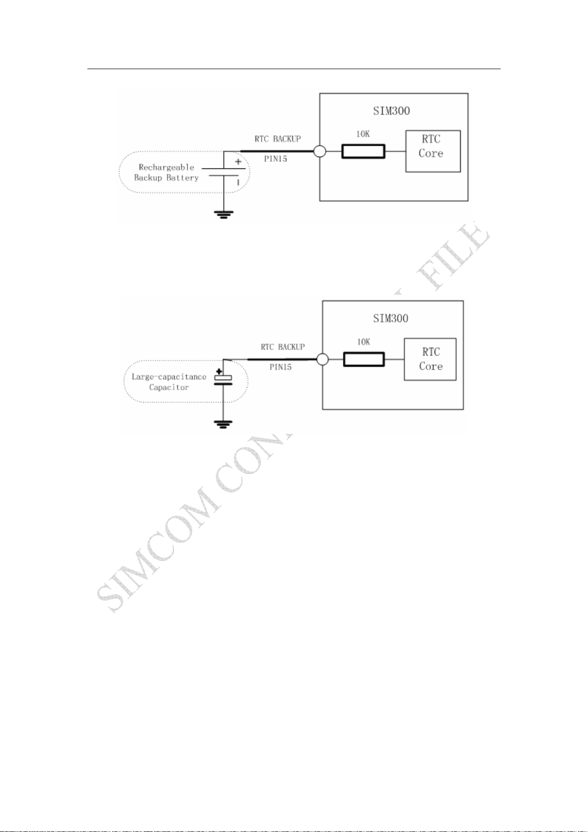
3.7 RTC backup
The RTC (Real Time Clock) power supply of module can be provided by an external battery or a
battery (rechargeable or non-chargeable) through the PIN15 on the board-to-board connector.
There is a 10K resistance has been integrated in SIM300 module used for restricting current. You
need only a coin-cell battery or a super-cap to PIN15 to backup power supply for RTC.
Note: The VRTC couldn’t be designed to a NC pin in your circuit. You should connect the
VRTC pin to a battery or a capacitor.
The following figures show various sample circuits for RTC backup.
6: RTC supply from non-chargeable battery
Figure
SIM300_HD_V3.02 Page 25 of 56
Page 26
SIM300 Hardware Interface Description
Confidential
SIMCOM
7: RTC supply from rechargeable battery
Figure
8: RTC supply from capacitor
Figure
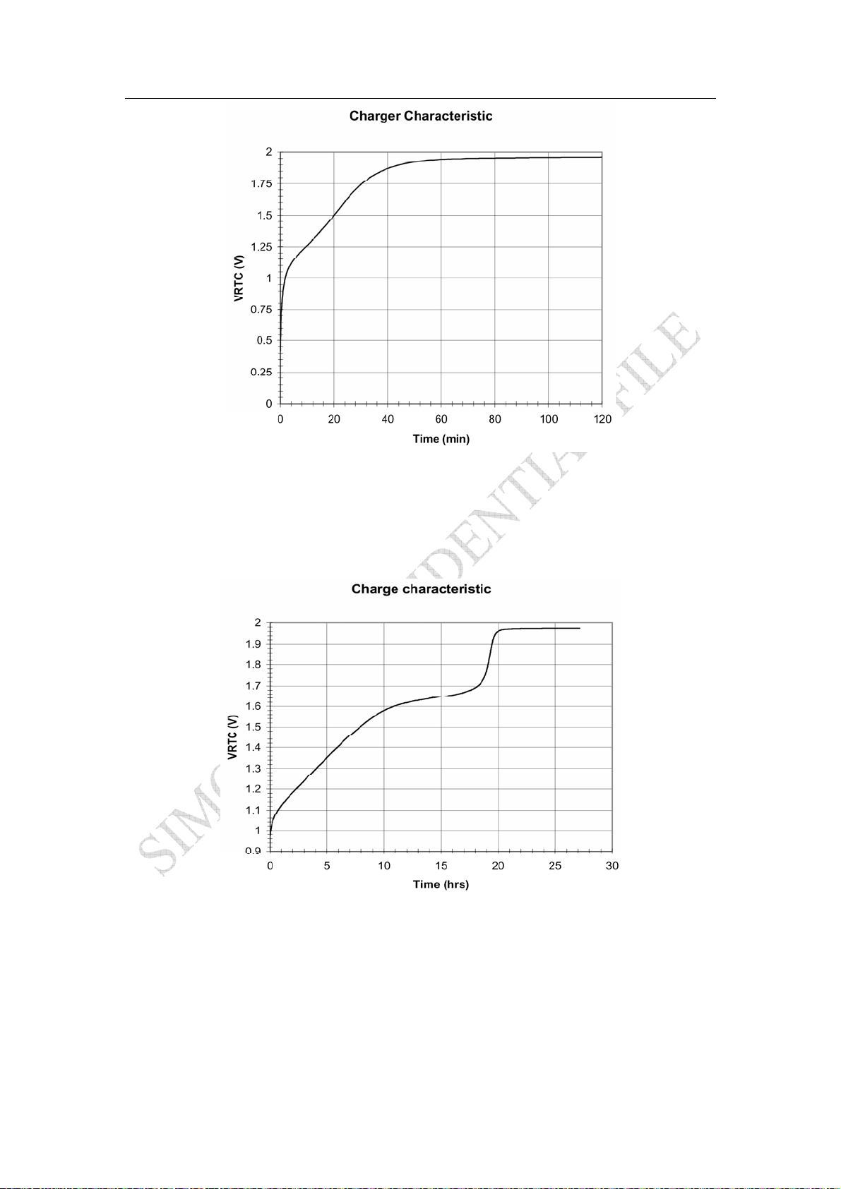
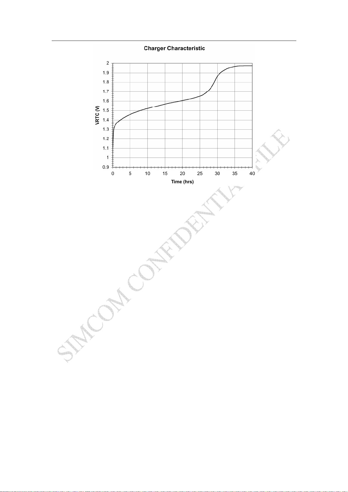
z Li-battery backup
Rechargeable Lithium coin cells such as the TC614 from Maxell, or the TS621 from Seiko, are
also small in size, but have higher capacity than the double layer capacitors resulting in longer
backup times.
Typical charge curves for each cell type are shown in following figures. Note that the rechargeable
Lithium type coin cells generally come pre-charged from the vendor.
SIM300_HD_V3.02 Page 26 of 56
Page 27
SIM300 Hardware Interface Description
Confidential
SIMCOM
Figure 9: Panasonic EECEMOE204A Charge Characteristic
Figure 10: Maxell TC614 Charge Characteristic
SIM300_HD_V3.02 Page 27 of 56
Page 28
SIM300 Hardware Interface Description
Confidential
SIMCOM
Figure 11: Seiko TS621 Charge Characteristic
Note:
Gold-capacitance backup
Some suitable coin cells are the electric double layer capacitors available from Seiko (XC621), or
from Panasonic (EECEM0E204A). They have a small physical size (6.8 mm diameter) and a
nominal capacity of 0.2 F to 0.3 F, giving hours of backup time.
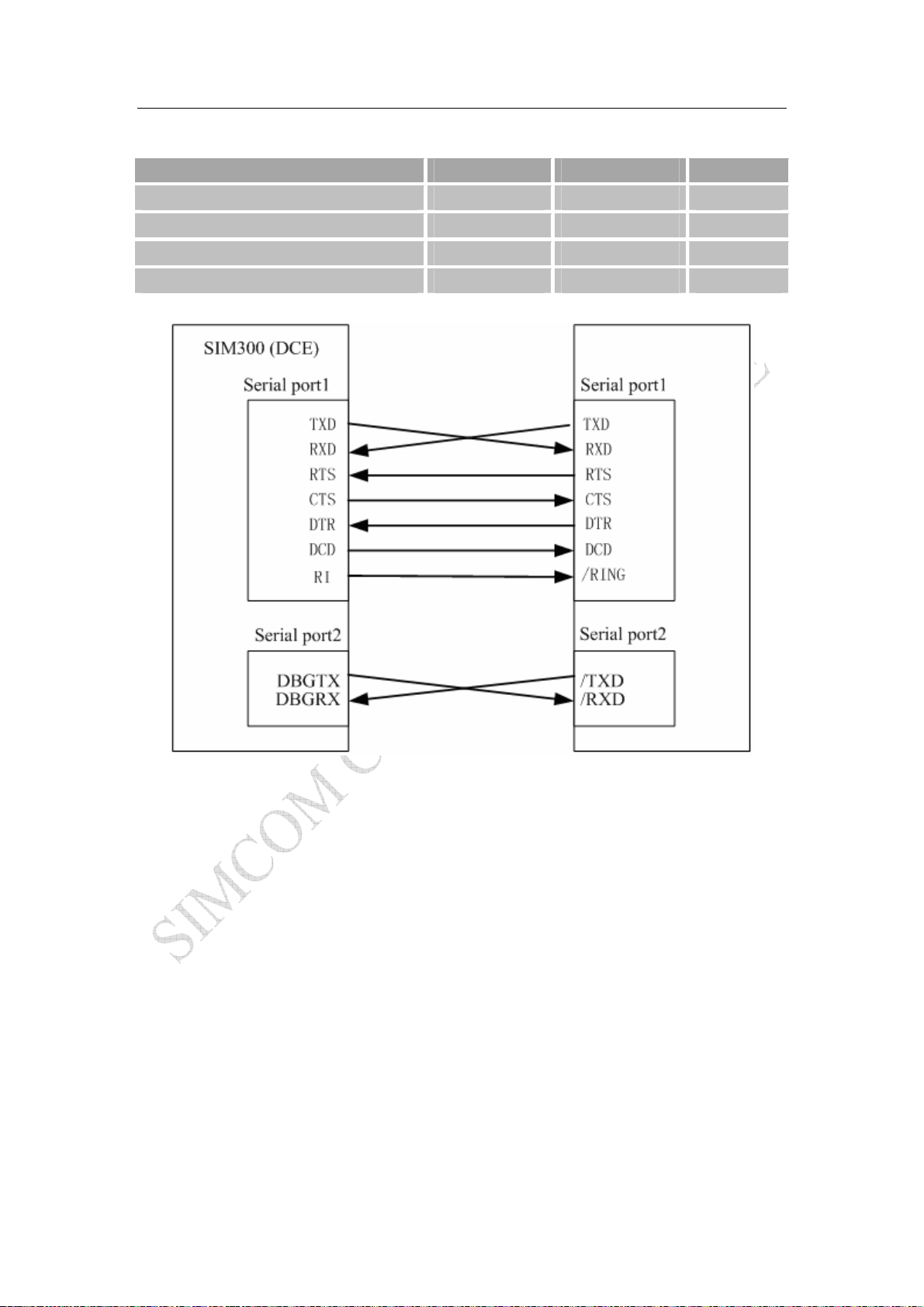
3.8 Serial interfaces
SIM300 provides two unbalanced asynchronous serial ports. The GSM module is designed as a
DCE (Data Communication Equipment), following the traditional DCE-DTE (Data Terminal
Equipment) connection, the module and the client (DTE) are connected through the following
signal (as following figure shows). Autobauding supports baud rate from 1200 bps to 115200bps.
Serial port 1
z Port/TXD @ Client sends data to the RXD signal line of module
z Port/RXD @ Client receives data from the TXD signal line of module
Serial port 2
z Port/TXD @ Client sends data to the DBGRX signal line of module
z Port/RXD @ Client receives data from the DBGTX signal line of module
All pins of two serial ports have 8mA driver, the logic levels are described in following table
SIM300_HD_V3.02 Page 28 of 56
Page 29
SIM300 Hardware Interface Description
Confidential
SIMCOM
Table 9: Logic levels of serial ports pins
Parameter Min Max Unit
Logic low input 0 0.3*VDD_EXT V
Logic high input 0.7 *VDD_EXT VDD_EXT +0.3 V
Logic low output GND 0.2 V
Logic high output VDD_EXT -0.2 VDD_EXT V
Figure 12:
Interface of serial ports
3.8.1 Function of Serial Port 1 & 2 supporting
Serial port 1
z Seven lines on Serial Port Interface
z Contains Data lines /TXD and /RXD, State lines /RTS and /CTS, Control lines /DTR, /DCD
and RING;
z Serial Port 1 can be used for CSD FAX, GPRS service and send AT command of controlling
module. Serial Port 1 can use multiplexing function, but you cannot use the Serial Port 2 at
the same time;
z Serial Port 1 supports the communication rate as following:
300, 1200, 2400, 4800, 9600, 19200, 38400, 57600, 115200 Default as 115200bps.
z Autobauding supports the communication rate as following:
1200, 2400, 4800, 9600, 19200, 38400, 57600, and 115200bps.
SIM300_HD_V3.02 Page 29 of 56
Page 30

SIM300 Hardware Interface Description
Confidential
SIMCOM
Autobauding allows the GSM engine to automatically detect the bit rate configured in the host
application. The serial interface of the GSM engine supports autobauding for the following bit
rates: 1200, 2400, 4800, 9600, 19200, 38400, 57600, 115200. Factory setting is autobauding
enabled. This gives you the flexibility to put the GSM engine into operation no matter what bit
rate your host application is configured to. To take advantage of autobaud mode specific attention
must be paid to the following requirements:
Synchronization between DTE and DCE.
Ensure that DTE and DCE are correctly synchronized and the bit rate used by the DTE is detected
by the DCE (= ME). To allow the bit rate to be synchronized simply issue an "AT" or "at" string.
This is necessary.
z after you have activated autobauding
z when you start up the GSM engine while autobauding is enabled. It is recommended to wait 3
to 5 seconds before sending the first AT character. Otherwise undefined characters might be
returned.
Restrictions on autobauding operation
z The serial interface has to be operated at 8 data bits, no parity and 1 stop bit (factory setting).
z The Unsolicited Result Codes like "RDY", "+CFUN: 1" and "+CPIN: READY” are not
indicated when you start up the ME while autobauding is enabled. This is due to the fact that
the new bit rate is not detected unless DTE and DCE are correctly synchronized as described
above.
Note: You can use AT+IPR=x;&W to set a fix baud rate and save the configuration to
non-volatile flash memory. After the configuration was saved as fix baud rate, the Unsolicited
Result Codes like "RDY" should be received from the serial port all the time when the SIM300
was power on.
Serial port 2
z Two lines on Serial Port Interface
z Only contains Data lines /TXD and /RXD
z Serial Port 2 only used for transmitting AT command. It cannot be used for CSD call, FAX
call. And the Serial port 2 can not use multiplexing function;
z Serial port 2 supports the communication rate as following:
9600, 19200, 38400, 57600, 115200
Note: You should configure the serial port2 by AT command of “AT+UART” before you can use
serial port2. Please refer to the “SIM300 Dual Serial Ports User Guide” and document [1] for
detail.
SIM300_HD_V3.02 Page 30 of 56
Page 31
SIM300 Hardware Interface Description
Confidential
SIMCOM
3.8.2 Software upgrade and Software debug
The TXD、RXD、DBGTX、DBGRX、GND must be connected to the IO connector when
user need to upgrade software and debug software, the TXD、RXD should be used for software
upgrade and the DBGTX、DBGRX for software debug. The PWRKEY pin is recommended to
connect to the IO connector. The user also can add a switch between the PWRKEY and the GND.
The PWRKEY should be connected to the GND when SIM300 is upgrading software. Please refer
to the following figures.
Figure 13: Interface of software upgrade
Figure 14: Interface of software debug
Note: The serial port doesn’t support the RS_232, it only supports the TTL level. You should add
the level converter IC between the DCE and DTE, if you connect it to the PC.
SIM300_HD_V3.02 Page 31 of 56
Page 32

SIM300 Hardware Interface Description
Confidential
SIMCOM
3.9 Audio interfaces
Table 10: Audio interface signal
Name Pin Function
(AIN1/AOUT1)
(AIN2/AOUT2)
The module provides two Analogy input channels, AIN1 and AIN2, which may be used for both
microphone and line inputs. The AIN1 and AIN2 channels are identical. One of the two channels
is typically used with a microphone built into a handset. The other channel is typically used with
an external microphone or external line input. The Module Analogy input configuration is
determined by control register settings and established using Analogy multiplexes.
For each channels, you can use AT+CMIC to set the input gain level of microphone, use
AT+ECHO to set the parameters for echo suppression. Also, you can use AT+SIDET to set the
side-tone level. For detail, please refer to [1].
It is suggested that you adopt the one of following two matching circuits in order to satisfy speaker
effect。 The difference audio signals have to be layout according to difference signal layout rules.
As show in following Figures(Note : all components package are 0603) .If you want to adopt a
amplifier circuit for audio, we commend National company’s LM4890. But you can select it
according to your needs.
Mic1p 53 Microphone1 input +
Mic1n 55 Microphone1 input -
Spk1p 54 Audio1 output+
Spk1n 56 Audio1 output-
Mic2p 57 Microphone2 input +
Mic2n 59 Microphone2 input -
Spk2p 58 Audio2 output+
Spk2n 60 Audio2 output-
SIM300_HD_V3.02 Page 32 of 56
Page 33

SIM300 Hardware Interface Description
Confidential
3.9.1 Speaker interface configuration
SIMCOM
Figure 15: Speaker interface configuration
Figure 16: Speaker interface with amplifier configuration
SIM300_HD_V3.02 Page 33 of 56
Page 34

SIM300 Hardware Interface Description
Confidential
3.9.2 Microphone interfaces configuration
SIMCOM
Figure 17: Microphone interface configuration
3.9.3 Earphone interface configuration
Figure 18: Earphone interface configuration
SIM300_HD_V3.02 Page 34 of 56
Page 35

SIM300 Hardware Interface Description
Confidential
3.9.4 Referenced Electronic Characteristic
SIMCOM
Table 11: MIC Input DC Characteristics
Parameter Min Typ Max Unit
Work i ng Vol tage 1.25 2.5 V
Working Current 5 300 uA
External
Microphone
Load Resistance
1.2 2.2 k Ohms
Table 12: Audio Output Characteristics
Parameter Min Typ Max Unit
Normal
Output(SPK1)
Auxiliary
Output(SPK2)
Ended
Differential
Ended
Differential
load
Resistance
Ref level 1.0954 Vpp
load
Resistance
Ref level 0.5477 Vpp
load
Resistance
Ref level 1.0954 Vpp
load
Resistance
Ref level 0.5477 Vpp
27 32 Ohm Single
27 32
27 32 Ohm Single
27 32
Table 13: Buzzer Output DC Characteristics
Parameter Min Typ Max Unit
Work i ng Vol tage 2.4 2.8 3.3 V
Working Current 8 mA
Load Resistance 1 k Ohms
3.10 Buzzer
The PIN 36 on the board-to-board connector can be used to drive a buzzer to indicate incoming
call. The output volume of buzzer can be set by “AT+CRSL”. The reference circuit for buzzer as
shown as following Figure:
SIM300_HD_V3.02 Page 35 of 56
Page 36

SIM300 Hardware Interface Description
Confidential
SIMCOM
Figure 19: Reference circuit for Buzzer
3.11 SIM card interface
3.11.1 SIM card application
You can use AT Command to get information in SIM card. For more information, please refer to
[1].
The SIM interface supports the functionality of the GSM Phase 1 specification and also supports
the functionality of the new GSM Phase 2+ specification for FAST 64 kbps SIM (intended for use
with a SIM application Tool-kit).
Both 1.8V and 3.0V SIM Cards are supported.
The SIM interface is powered from an internal regulator in the module having nominal voltage
2.8V. All pins reset as outputs driving low. Logic levels are as described in table
SIM300_HD_V3.02 Page 36 of 56
Page 37

SIM300 Hardware Interface Description
Confidential
Table 14: Signal of SIM interface (board-to-board connector)
Pin Signal Description
19 SIM_VDD SIM Card Power output automatic output on SIM mode,one is
21 SIM_I/O SIM Card data I/O
23 SIM_CLK SIM Card Clock
25 SIM_RST SIM Card Reset
16 SIM_PRESENCE SIM Card Presence
Following is the reference circuit about SIM interface. We recommend an Electro-Static discharge
device ST (
ANTI”. The 22Ω resistors showed in the following figure should be added in series on the IO line
between the module and the SIM card for matching the impedance. The pull up resistor (about
10KΩ) must be added on the SIM_I/O line. Note that the SIM peripheral circuit close to the SIM
card socket.
The SIM_PRESENCE pin is used for detecting the SIM card removal. You can use the AT
command “AT+CSDT” to set the SIMCARD configure. For detail of this AT command, please
refer to
You can select the 8 pins SIM card. The reference circuit about 8 pins SIM card illustrates as
following figure.
SIMCOM
3.0V±10%, another is 1.8V±10%. Current is about 10mA.
www.st.com ) ESDA6V1W5 or ON SEMI (www.onsemi.com ) SMF05C for “ESD
document [1]:
Figure 20: SIM interface reference circuit with 8 pins SIM card
If you don’t use the SIM card detection function, you can let the SIM_PRESENCE pin NC or
connect to the GND. The reference circuit about 6 pins SIM card illustrate as following figure.
SIM300_HD_V3.02 Page 37 of 56
Page 38

SIM300 Hardware Interface Description
Confidential
SIMCOM
Figure 21: SIM interface reference circuit with 6 pins SIM card
3.11.2 Design considerations for SIM card holder
For 6 pins SIM card, we recommend to use Amphenol C707 10M006 512 2 .You can visit
http://www.amphenol.com for more information about the holder.
Figure 22: Amphenol C707 10M006 512 2 SIM card holder
SIM300_HD_V3.02 Page 38 of 56
Page 39
SIM300 Hardware Interface Description
Confidential
SIMCOM
Table 15: Pin description (Amphenol SIM card holder)
Pin Signal Description
SIM Card Power supply, it can identify automatically the SIM
C1
SIM_VDD
Card power mode,one is 3.0V±10%, another is 1.8V±10%.
Current is about 10mA.
C2
C3
C5
C6
C7
SIM_RST SIM Card Reset.
SIM_CLK SIM Card Clock.
GND Connect to GND.
VPP Not connect.
SIM_I/O SIM Card data I/O.
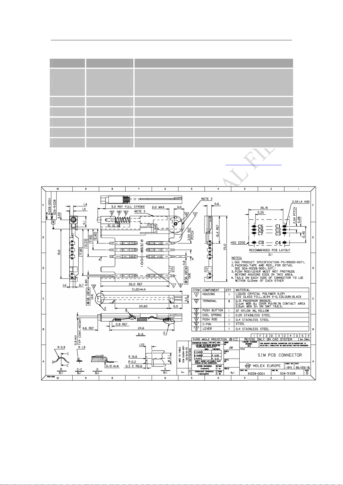
For 8 pins SIM card, we recommend to use Molex 91228.You can visit
for more information about the holder.
http://www.molex.com
Figure 23: Molex 91228 SIM card holder
SIM300_HD_V3.02 Page 39 of 56
Page 40

SIM300 Hardware Interface Description
Confidential
SIMCOM
Table 16: Pin description (Molex SIM card holder)
Pin Signal Description
C1
C2
C3
C4
C5
C6
C7
C8
SIM_VDD SIM Card Power supply, it can identify
automatically the SIM Card power mode,one is
3.0V±10%, another is 1.8V±10%. Current is
about 10mA.
SIM_RST SIM Card Reset.
SIM_CLK SIM Card Clock.
GND Connect to GND.
GND Connect to GND.
VPP Not connect.
SIM_I/O SIM Card data I/O.
SIM_PRESENCE Detect SIM Card Presence
3.12 LCD interface
SIM300 provides a serial LCD display interface that supports serial communication with LCD
device. These are composite pins that can be used as GPIO ports or LCD display interface
according to your application. When use as LCD interface, the following table is the pin
define. LCD interface timing should be united with the LCD device.
Table 17: PIN define of LCD interface
Pin (On board-to-board connector) Name Function
18 SPI_DATA Display data output
20 SPI_CLK Display clock for LCD
22 SPI_CS Display enable
24 SPI_D/C Display data or address select
26 SPI_RST LCD reset
3.13 ADC
SIM300 provides one auxiliary ADC (General purpose analog to digital converter.) as voltage
input pin, which can be used to detect the values of some external items such as voltage,
temperature etc. User can use AT command “AT+CADC” to read the voltage value added on
ADC pin. For detail of this AT command, please refer to document [1]].
SIM300_HD_V3.02 Page 40 of 56
Page 41
SIM300 Hardware Interface Description
Confidential
Table 18: ADC pin of SIM300
Name Pin (On board-to-board connector) Input voltage scope( V )
ADC0 52 0 – 2.4
SIMCOM
3.14 Behaviors of the /RING line (Serial port1 interface only)
Table 19: Behaviours of the /RING line
State RI respond
Standby
Voice calling Change low, then:
Data calling Change low,then:
SMS
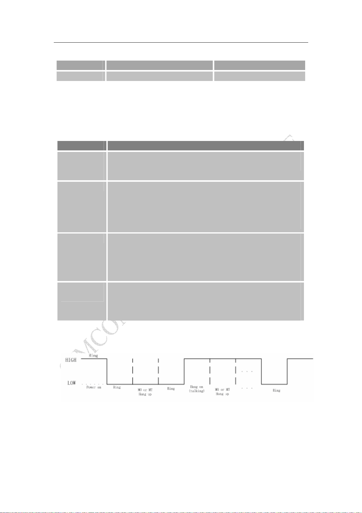
If the module is used as caller, signal ring will maintain high. But when it is used as receiver,
following is timing of ring.
High
(1)Change to high when establish calling.
(2)Use AT command ATH the RING hold low.
(3)Sender hang up, change to high
(1)Change to high when establish calling.
(2)Use AT command ATH the RING hold low.
When receive SMS, the ring will change to LOW and hold LOW level at
least 100 ms, then change to HIGH.
Figure 24: SIM300 Services as Receiver
SIM300_HD_V3.02 Page 41 of 56
Page 42
SIM300 Hardware Interface Description
Confidential
SIMCOM
Figure 25: SIM300 Services as caller
3.15 Network status indication LED lamp
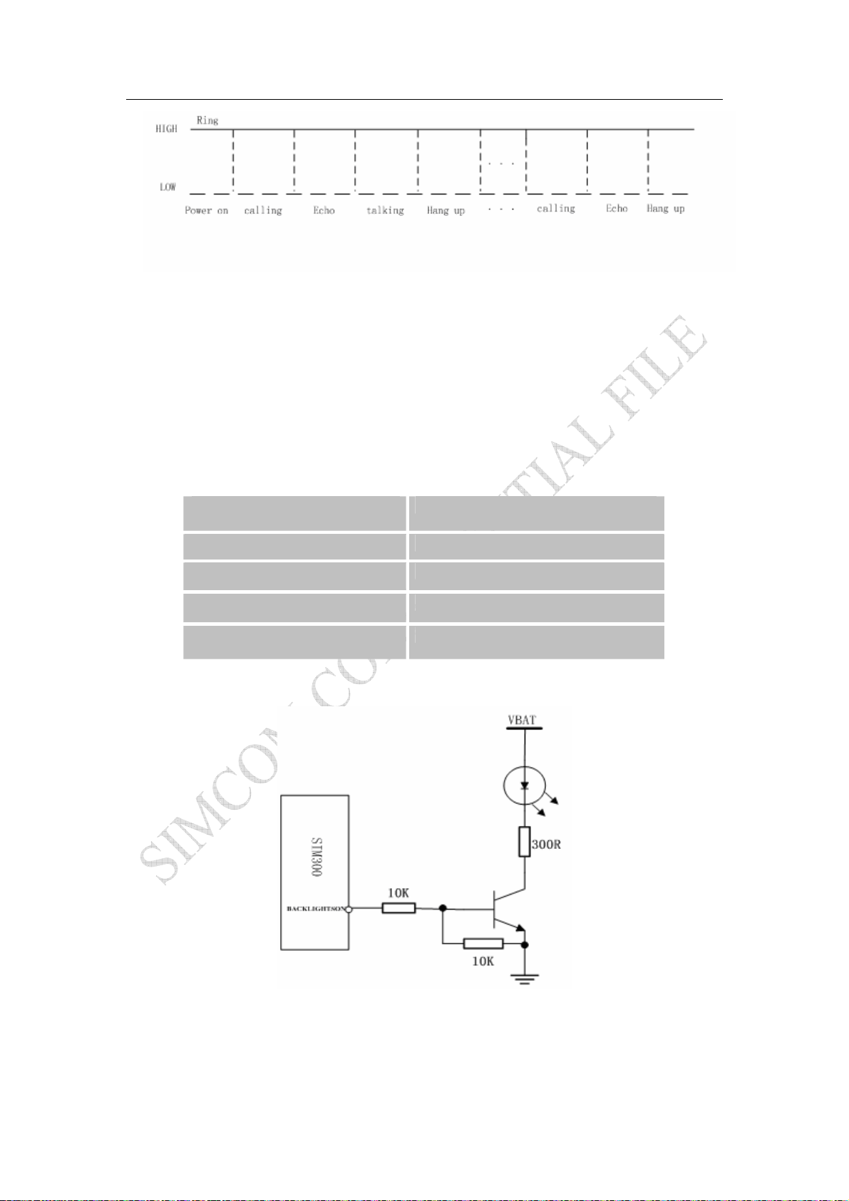
The PIN 30 on the board-to-board connector can be used to drive a network status indication LED
lamp. The working state of this pin is listed in following table:
Table 20: Working state of network status indication LED pin
State SIM300 function
Off SIM300 is not running
64ms On/ 800ms Off SIM300 does not find the network
64ms On/ 3000ms Off SIM300 find the network
64ms On/ 300ms Off GPRS communication
We provide a reference circuitry for you, show as following Figure:
Figure 26: Reference circuit for Network status LED
SIM300_HD_V3.02 Page 42 of 56
Page 43

SIM300 Hardware Interface Description
Confidential
SIMCOM
3.16 General Purpose Input Output (GPIO)
SIM300 provides a limited number of General Purpose Input/Output signal pins.
Table
21: GPIO Pins of SIM300
Pin Name Function
32 GPIO5 General Purpose Input/Output Port
36 GPIO8 General Purpose Input/Output Port
SIM300_HD_V3.02 Page 43 of 56
Page 44

SIM300 Hardware Interface Description
Confidential
SIMCOM
4 Antenna interface
The RF interface has an impedance of 50Ω. To suit the physical design of individual applications
SIM300 offers two alternatives:
z Recommended approach: antenna connector on the component side of the PCB
z Antenna pad and grounding plane placed on the bottom side.
To minimize the loss on the RF cable, it need be very careful to choose RF cable. We recommend
the insertion loss should be meet following requirement:
z GSM900<1dB
z DCS1800/PCS1900<1.5dB
4.1 Antenna installation
4.1.1 Antenna connector
SIM300 use MURATA’s MM9329-2700 RF connector on the module side, we recommend user
use MURATA’s MXTK92XXXXX as matching connector on the application side. Please refer to
appendix for detail info about MURATA’s MXTK92XXXXX.
4.1.2 Antenna pad
The antenna can be soldered to the pad, or attached via contact springs. To help you to ground the
antenna, SIM300 comes with a grounding plane located close to the antenna pad.
SIM300 material properties:
SIM300 PCB Material: FR4
Antenna pad: Gold plated pad
Antenna pad soldering temperature (fewer 10 seconds): 260°C
4.2 Module RF output power
Table 22: SIM300 RF output power
Frequency Max Min
E-GSM900 33dBm ±2db 5dBm±5db
DCS1800 30dBm ±2db 0dBm±5db
PCS1900 30dBm ±2db 0dBm±5db
SIM300_HD_V3.02 Page 44 of 56
Page 45

SIM300 Hardware Interface Description
Confidential
SIMCOM
4.3 Module RF receive sensitivity
Table 23: SIM300 RF receive sensitivity
Frequency Receive sensitivity
E-GSM900 < -106dBm
DCS1800 < -104dBm
PCS1900 < -104dBm
4.4 Module receive/transmit frequency
Table 24: SIM300 receive/transmit frequency
Frequency Receive Transmit
E-GSM900 925 ~ 960MHz 880 ~ 915MHz
DCS1800 1805 ~ 1880MHz 1710 ~ 1785MHz
PCS1900 1930 ~ 1990MHz 1850 ~ 1910MHz
4.5 Antenna gain
Table 25: Antenna gain
Item parameter
GSM DCS
Gain(dBi)
0.5 1
Pattern Omnidirectional antenna
SIM300_HD_V3.02 Page 45 of 56
Page 46
SIM300 Hardware Interface Description
Confidential
SIMCOM
5 Electrical, reliability and radio characteristics
5.1 Absolute maximum ratings
Absolute maximum rating for power supply and voltage on digital and analog pins of SIM300 are
list in following table:
Table 26: Absolute maximum ratings
Parameter Min Max Unit
Peak current of power supply 0 4.0 A
RMS current of power supply (during one TDMA- frame) 0 0.7 A
Voltage at digit pins -0.3 3.3 V
Voltage at analog pins -0.3 3.0 V
Voltage at digit/analog pins in POWER DOWN mode -0.25 0.25 V
5.2 Operating temperatures
The operating temperature is listed in following table:
Table 27: SIM300 operating temperature
Parameter Min Typ Max Unit
Ambient temperature -20 25 55 ℃
Restricted operation* -30 to -20 55 to 80 ℃
Storage temperature -40 +85 ℃
* SIM300 can work, but the deviation from the GSM specification may occur.
SIM300_HD_V3.02 Page 46 of 56
Page 47

SIM300 Hardware Interface Description
Confidential
SIMCOM
5.3 Power supply ratings
Table 28: SIM300 power supply ratings
Parameter Description Conditions Min Typ Max Unit
VBAT Supply voltage Voltage must stay within the
min/max values, including
voltage drop, ripple, and spikes.
Voltage drop
during transmit
burst
Voltage ripple Normal condition, power
I
VBAT
Average supply
current
Normal condition, power
control level for Pout max
control level for Pout max
@ f<200kHz
@ f>200kHz
POWER DOWN mode
SLEEP mode
IDLE mode
EGSM 900
GSM 1800/1900
TALK mode
EGSM 900
GSM 1800/1900
DATA mode, GPRS (3 Rx,2Tx)
EGSM 900
GSM 1800/1900
DATA mode, GPRS (4 Rx,1Tx)
EGSM 900
GSM 1800/1900
3.4 4.0 4.5 V
400 mV
35
3
23
23
260
190
490
340
290
220
50
2
mV
uA
mA
mA
mA
mA
mA
Peak supply
current (during
transmission
slot every 4.6ms)
SIM300_HD_V3.02 Page 47 of 56
Power control level 2 3 A
Page 48
SIM300 Hardware Interface Description
Confidential
SIMCOM
5.4 Current Consumption
The values for current consumption listed below refer to Table 29.
Table 29: SIM300 current consumption
Voice Call
GSM 900 @power level #5 <350mA,Typical 260mA
@power level #10,Typical 130mA
@power level #19,Typical 86mA
GSM1800/1900 @power level #0 <300mA,Typical 200mA
@power level #10,Typical 87mA
@power level #15,Typical 80mA
GPRS Data
DATA mode, GPRS ( 1 Rx,1 Tx ) CLASS 8
GSM 900 @power level #5 <350mA,Typical 260mA
@power level #10,Typical 125mA
@power level #19,Typical 84mA
GSM1800/1900 @power level #0 <300mA,Typical 200mA
@power level #10,Typical 83mA
@power level #15,Typical 76mA
DATA mode, GPRS ( 3 Rx, 2 Tx ) CLASS 10
GSM 900 @power level #5 <550mA,Typical 470mA
@power level #10,Typical 225mA
@power level #19,Typical 142mA
GSM1800/1900 @power level #0 <450mA,Typical 340mA
@power level #10,Typical 140mA
@power level #15,Typical 127mA
DATA mode, GPRS ( 4 Rx,1 Tx ) CLASS 8
GSM 900 @power level #5 <350mA,Typical 270mA
@power level #10,Typical 160mA
@power level #19,Typical 120mA
GSM1800/1900 @power level #0 <300mA,Typical 220mA
@power level #10,Typical 120mA
@power level #15,Typical 113mA
Class 8 is default set when the module work at data translation mode, the module can also work at
class 10 set by AT command. But the module power consumption will be added a little.
SIM300_HD_V3.02 Page 48 of 56
Page 49

SIM300 Hardware Interface Description
Confidential
SIMCOM
5.5 Electro-Static discharge
Normally the module is designed inside customer terminal, so about Electro-Static Discharge
(ESD) should be considered base on the requirement of terminal product. But for the module is
protected against Electro-Static Discharge in conveyance and customer production, and some
second level ESD protect design inside module.
The remaining ports are not special ESD protection in module, so the user should consider in the
final product, and therefore, they are only protected according to the Human Body Model
requirements.
Table 30: The ESD endure statue measured table (Temperature: 25 , Humidity:45% )℃
Part Contact discharge Air discharge
VBAT,GND ±4KV ±8KV
KBR0-4, DTR, RXD, TXD, RTS,
SPI_DATA, SPI_CLK
Antenna port
Other port ±1KV
±2KV ±4KV
±2KV ±4KV
SIM300_HD_V3.02 Page 49 of 56
Page 50

SIM300 Hardware Interface Description
Confidential
SIMCOM
6 Mechanics
This chapter describes the mechanical dimensions of SIM300.
6.1 Mechanical dimensions of SIM300
Following are SIM300 top view, side view and bottom view. These show you Mechanical
dimensions of SIM300.
Figure 27: Mechanical dimensions of SIM300(Unit: mm)
SIM300_HD_V3.02 Page 50 of 56
Page 51

SIM300 Hardware Interface Description
Confidential
SIMCOM
6.2 Mounting SIM300 onto the application platform
Use the connector ENTERY 1008-G60N-01R and four mounting pads fix the SIM300 onto
customer platform.
6.3 Board-to-board connector
We recommend user adopt ENTERY Company’s 1008-G60N-01R as the Board to board
connector. These high density SMT connectors are designed for parallel PCB-to-PCB applications.
They are ideal for use in VCRs, notebook PCs, cordless telephones, mobile phones, audio/visual
and other telecommunications equipment where reduced size and weight are important. Following
is parameter of 1008-G60N-01R. For more, you can login http://www.entery.com.tw for more
information.
6.3.1 Mechanical dimensions of the ENTERY 1008-G60N-01R
Figure 28: ENTERY 1008-G60N-01R board-to-board connector pin side
SIM300_HD_V3.02 Page 51 of 56
Page 52

SIM300 Hardware Interface Description
Confidential
SIMCOM
Figure 29: ENTERY board to board connector physical photo
NOTE:
The connector ENTERY 1009
ENTERY 1008
-G60N-01R is used pin side (user side).
-G60N-01R is used in socket side (SIM300 module) and
SIM300_HD_V3.02 Page 52 of 56
Page 53

SIM300 Hardware Interface Description
Confidential
SIMCOM
6.4 RF Adapter cabling
The RF connector in module side is Murata Company Microwave Coaxial Connectors
MM9329-2700B, it makes a pair with Murata Company RF connector MXTK. It is have high
performance with wide frequency range, surface mountable and reflow solderable. Following is
parameter. Certainly you can visit
http://www.murata.com/ for more information.
Figure 30: MM9329-2700B
SIM300_HD_V3.02 Page 53 of 56
Page 54

SIM300 Hardware Interface Description
Confidential
SIMCOM
Figure 31: RF connector MXTK
For more information about the connector, please visit
http://www.murata.com/
SIM300_HD_V3.02 Page 54 of 56
Page 55
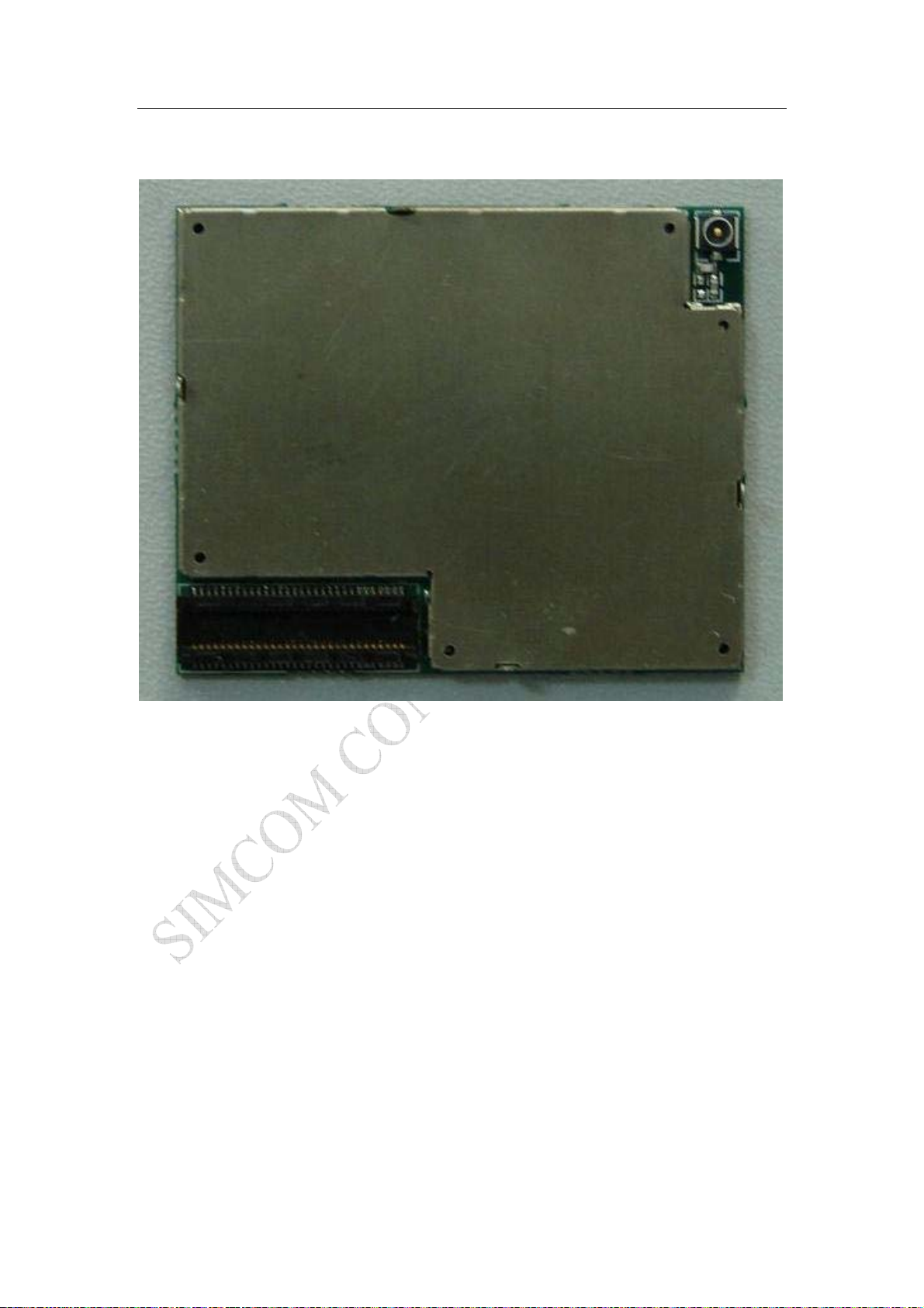
SIM300 Hardware Interface Description
Confidential
SIMCOM
6.5 Top view of the SIM300
SIM300_HD_V3.02 Page 55 of 56
Page 56

SIM300 Hardware Interface Description
Confidential
SIMCOM
6.6 PIN assignment of board-to-board connector of SIM300
Table 31: Connection diagrams
PIN NO. PIN NAME I/O PIN NO. PIN NAME I/O
2
4
6
8
10
12
14
16
18
20
22
24
26
28
30
32
34
VBAT I
VBAT I
VBAT I
VBAT I
GND
GND
GND
SIM_PRESENCE I
SPI_DATA I/O
SPI_CLK O
SPI_CS O
SPI_D/C O
SPI_RST O
DCD/GPIO0 O
Network LED /GPIO1 O
GPIO5 I/O
PWRKEY I
1
3
5
7
9
11
13
15
17
19
21
23
25
27
29
31
33
VBAT I
VBAT I
VBAT I
VBAT I
GND
GND
GND
VRTC I/O
VDD_EXT O
SIM_VDD O
SIM_I/O I/O
SIM_CLK O
SIM_RST O
KBC0 O
KBC1 O
KBC2 O
KBC3 O
36
38
40
42
44
46
48
50
52
54
56
58
60
Buzzer/GPIO8
DTR I
RXD I
TXD O
RTS I
CTS O
RI O
AGND I/O
ADC0 I
SPK1P O
SPK1N O
SPK2P O
SPK2N O
35
37
39
41
43
45
47
49
51
53
55
57
59
KBC4 O
KBR0 I
KBR1 I
KBR2 I
KBR3 I
KBR4 I
DBGRX I
DBGTX O
AGND I/O
MIC1P I
MIC1N I
MIC2P I
MIC2N I
SIM300_HD_V3.02 Page 56 of 56
 Loading...