


Silicon Storage Technology Inc SST89V564RC-25-C-PJ, SST89V564RC-25-C-PI, SST89V564RC-25-C-NJ, SST89V564RC-25-C-NI, SST89V564RD-40-C-NI Datasheet
...FlashFlex51 MCU
SST89E564RD / SST89V564RD / SST89E554RC / SST89V554RC
Preliminary Specifications
FEATURES:
•8-bit 8051 Family Compatible Microcontroller (MCU) with Embedded SuperFlash Memory
•SST89E564RD/SST89E554RC is 5V Operation
–0 to 40 MHz Operation at 5V
•SST89V564RD/SST89V554RC is 3V Operation
–0 to 25 MHz Operation at 3V
•Fully Software and Development Toolset Compatible as well as Pin-For-Pin Package Compatible with Standard 8xC5x Microcontrollers
•1 KByte Register/Data RAM
•Dual Block SuperFlash EEPROM
–SST89E564RD/SST89V564RD: 64 KByte primary block + 8 KByte secondary block (128-Byte sector size)
–SST89E554RC/SST89V554RC: 32 KByte primary block + 8 KByte secondary block (128-Byte sector size)
–Individual Block Security Lock
–Concurrent Operation during In-Application Programming (IAP)
–Block Address Re-mapping
•Support External Address Range up to 64 KByte of Program and Data Memory
•Three High-Current Drive Pins (16 mA each)
•Three 16-bit Timers/Counters
•Full-Duplex Enhanced UART
–Framing error detection
–Automatic address recognition
•Nine Interrupt Sources at 4 Priority Levels
•Watchdog Timer (WDT)
•Programmable Counter Array (PCA)
•Four 8-bit I/O Ports (32 I/O Pins)
•Second DPTR register
•Reduce EMI Mode (Inhibit ALE through AUXR SFR)
•SPI Serial Interface
•TTLand CMOS-Compatible Logic Levels
•Brown-out Detection
•Extended Power-Saving Modes
–Idle Mode
–Power Down Mode with External Interrupt Wake-up
–Standby (Stop Clock) Mode
•PDIP-40, PLCC-44 and TQFP-44 Packages
•Temperature Ranges:
–Commercial (0°C to +70°C)
–Industrial (-40°C to +85°C)
PRODUCT DESCRIPTION
SST89E564RD, SST89V564RD, SST89E554RC, and SST89V554RC are members of the FlashFlex51 family of 8- bit microcontrollers. The FlashFlex51 is a family of microcontroller products designed and manufactured on the state-of- the-art SuperFlash CMOS semiconductor process technology. The device uses the same powerful instruction set and is pin-for-pin compatible with standard 8xC5x microcontroller devices.
The device comes with 72/40 KByte of on-chip flash EEPROM program memory using SST’s patented and proprietary CMOS SuperFlash EEPROM technology with the SST’s field-enhancing, tunneling injector, split-gate memory cells. The SuperFlash memory is partitioned into 2 independent program memory blocks. The primary SuperFlash Block 0 occupies 64/32 KByte of internal program memory space and the secondary SuperFlash Block 1 occupies 8 KByte of internal program memory space. The 8-KByte secondary SuperFlash block can be mapped to the lowest location of the 64/32 KByte address space; it can also be hidden from the program counter and used as an independent EEPROM-like data memory. The flash memory blocks can be programmed via a standard 87C5x OTP EPROM programmer fitted with a special adapter and
firmware for SST’s device. During the power-on reset, the device can be configured as a slave to an external host for source code storage or as a master to an external host for In-Application Programming (IAP) operation. The device is designed to be programmed “In-System” and “In-Applica- tion” on the printed circuit board for maximum flexibility. The device is pre-programmed with an example of bootstrap loader in the memory, demonstrating the initial user program code loading or subsequent user code updating via the “IAP” operation. An example of bootstrap loader is for the user’s reference and convenience only. SST does not guarantee the functionality or the usefulness of the sample bootstrap loader. Chip-Erase or Block-Erase operations will erase the pre-programmed sample code.
In addition to 72/40 KByte of SuperFlash EEPROM program memory on-chip, the device can address up to 64 KByte of external program memory. In addition to 1024 x 8 bits of on-chip RAM, up to 64 KByte of external RAM can be addressed.
SST’s highly reliable, patented SuperFlash technology and memory cell architecture have a number of important advantages for designing and manufacturing flash EEPROMs. These advantages translate into significant cost and reliability benefits for our customers.
©2001 Silicon Storage Technology, Inc. |
The SST logo and SuperFlash are registered trademarks of Silicon Storage Technology, Inc. |
|
S71207-00-000 9/01 |
555 |
FlashFlex, In-Application Programming, IAP, and SoftLock are trademarks of Silicon Storage Technology, Inc. |
|
|
These specifications are subject to change without notice. |

FlashFlex51 MCU
SST89E564RD / SST89V564RD / SST89E554RC / SST89V554RC
Preliminary Specifications
TABLE OF CONTENTS
PRODUCT DESCRIPTION . . . . . . . . . . . . . . . . . . . . . . . . . . . . . . . . . . . . . . . . . . . . . . . . . . . . . . . . . . . . . . . . . . . 1
LIST OF FIGURES . . . . . . . . . . . . . . . . . . . . . . . . . . . . . . . . . . . . . . . . . . . . . . . . . . . . . . . . . . . . . . . . . . . . . . . . . |
4 |
LIST OF TABLES. . . . . . . . . . . . . . . . . . . . . . . . . . . . . . . . . . . . . . . . . . . . . . . . . . . . . . . . . . . . . . . . . . . . . . . . . . . 5
1.0 FUNCTIONAL BLOCKS . . . . . . . . . . . . . . . . . . . . . . . . . . . . . . . . . . . . . . . . . . . . . . . . . . . . . . . . . . . . . . . . . 6
Functional Block Diagram . . . . . . . . . . . . . . . . . . . . . . . . . . . . . . . . . . . . . . . . . . . . . . . . . . . . . . . . . . . . . . . . 6
2.0 PIN ASSIGNMENTS. . . . . . . . . . . . . . . . . . . . . . . . . . . . . . . . . . . . . . . . . . . . . . . . . . . . . . . . . . . . . . . . . . . . 7
2.1 Pin Descriptions . . . . . . . . . . . . . . . . . . . . . . . . . . . . . . . . . . . . . . . . . . . . . . . . . . . . . . . . . . . . . . . . . . . . 8
3.0 MEMORY ORGANIZATION . . . . . . . . . . . . . . . . . . . . . . . . . . . . . . . . . . . . . . . . . . . . . . . . . . . . . . . . . . . . . 10
3.1 Program Memory . . . . . . . . . . . . . . . . . . . . . . . . . . . . . . . . . . . . . . . . . . . . . . . . . . . . . . . . . . . . . . . . . . 10
3.2 Program Memory Block Switching . . . . . . . . . . . . . . . . . . . . . . . . . . . . . . . . . . . . . . . . . . . . . . . . . . . . . 11
3.2.1 Reset Configuration of Program Memory Block Switching. . . . . . . . . . . . . . . . . . . . . . . . . . . . . . 12
3.3 Data Memory . . . . . . . . . . . . . . . . . . . . . . . . . . . . . . . . . . . . . . . . . . . . . . . . . . . . . . . . . . . . . . . . . . . . . 12
3.4 Dual Data Pointers . . . . . . . . . . . . . . . . . . . . . . . . . . . . . . . . . . . . . . . . . . . . . . . . . . . . . . . . . . . . . . . . . 12
3.5 Special Function Registers (SFR) . . . . . . . . . . . . . . . . . . . . . . . . . . . . . . . . . . . . . . . . . . . . . . . . . . . . . 12
4.0 FLASH MEMORY PROGRAMMING . . . . . . . . . . . . . . . . . . . . . . . . . . . . . . . . . . . . . . . . . . . . . . . . . . . . . . 27
4.1 External Host Programming Mode . . . . . . . . . . . . . . . . . . . . . . . . . . . . . . . . . . . . . . . . . . . . . . . . . . . . . 27
4.1.1 Product Identification . . . . . . . . . . . . . . . . . . . . . . . . . . . . . . . . . . . . . . . . . . . . . . . . . . . . . . . . . . |
29 |
4.1.2 Arming Command . . . . . . . . . . . . . . . . . . . . . . . . . . . . . . . . . . . . . . . . . . . . . . . . . . . . . . . . . . . . |
29 |
4.1.3 Detail Explanation of the External Host Mode Commands . . . . . . . . . . . . . . . . . . . . . . . . . . . . . |
29 |
4.1.4 External Host Mode Clock Source . . . . . . . . . . . . . . . . . . . . . . . . . . . . . . . . . . . . . . . . . . . . . . . . |
30 |
4.1.5 Flash Operation Status Detection Via External Host Handshake . . . . . . . . . . . . . . . . . . . . . . . . |
30 |
4.1.6 Step-by-step instructions to perform |
|
External Host Mode commands . . . . . . . . . . . . . . . . . . . . . . . . . . . . . . . . . . . . . . . . . . . . . . . . . . . . . . . |
30 |
4.1.7 Flash Memory Programming Timing Diagrams with External Host Mode . . . . . . . . . . . . . . . . . . |
31 |
4.2 In-Application Programming Mode. . . . . . . . . . . . . . . . . . . . . . . . . . . . . . . . . . . . . . . . . . . . . . . . . . . . . 36
4.2.1 In-Application Programming Mode Clock Source. . . . . . . . . . . . . . . . . . . . . . . . . . . . . . . . . . . . . 36 4.2.2 Memory Bank Selection for In-Application Programming Mode. . . . . . . . . . . . . . . . . . . . . . . . . . 36 4.2.3 IAP Enable Bit . . . . . . . . . . . . . . . . . . . . . . . . . . . . . . . . . . . . . . . . . . . . . . . . . . . . . . . . . . . . . . . 36 4.2.4 In-Application Programming Mode Commands . . . . . . . . . . . . . . . . . . . . . . . . . . . . . . . . . . . . . . 36 4.2.5 Polling. . . . . . . . . . . . . . . . . . . . . . . . . . . . . . . . . . . . . . . . . . . . . . . . . . . . . . . . . . . . . . . . . . . . . . 37 4.2.6 Interrupt Termination . . . . . . . . . . . . . . . . . . . . . . . . . . . . . . . . . . . . . . . . . . . . . . . . . . . . . . . . . . 37
5.0 TIMERS/COUNTERS . . . . . . . . . . . . . . . . . . . . . . . . . . . . . . . . . . . . . . . . . . . . . . . . . . . . . . . . . . . . . . . . . . 39
6.0 SERIAL I/O . . . . . . . . . . . . . . . . . . . . . . . . . . . . . . . . . . . . . . . . . . . . . . . . . . . . . . . . . . . . . . . . . . . . . . . . . . 39
6.1 Enhanced Universal Asynchronous Receiver/Transmitter (UART) . . . . . . . . . . . . . . . . . . . . . . . . . . . . 39
6.1.1 Framing Error Detection . . . . . . . . . . . . . . . . . . . . . . . . . . . . . . . . . . . . . . . . . . . . . . . . . . . . . . . . 39
6.1.2 Automatic Address Recognition . . . . . . . . . . . . . . . . . . . . . . . . . . . . . . . . . . . . . . . . . . . . . . . . . . 39
6.2 Serial Peripheral Interface (SPI) . . . . . . . . . . . . . . . . . . . . . . . . . . . . . . . . . . . . . . . . . . . . . . . . . . . . . . 40
©2001 Silicon Storage Technology, Inc. |
S71207-00-000 9/01 555 |
2

FlashFlex51 MCU
SST89E564RD / SST89V564RD / SST89E554RC / SST89V554RC
Preliminary Specifications
7.0 |
WATCHDOG TIMER . . . . . . . . . . . . . . . . . . . . . . . . . . . . . . . . . . . . . . . . . . . . . . . . . . . . . . . . . . . . . . . . . . |
42 |
|
8.0 |
PROGRAMMABLE COUNTER ARRAY (PCA) . . . . . . . . . . . . . . . . . . . . . . . . . . . . . . . . . . . . . . . . . . . . . . |
43 |
|
|
8.1 |
PCA Timer/Counter . . . . . . . . . . . . . . . . . . . . . . . . . . . . . . . . . . . . . . . . . . . . . . . . . . . . . . . . . . . . . . . . |
43 |
|
8.2 |
PCA Compare/Capture Modules . . . . . . . . . . . . . . . . . . . . . . . . . . . . . . . . . . . . . . . . . . . . . . . . . . . . . . |
43 |
|
|
8.2.1 Capture Mode. . . . . . . . . . . . . . . . . . . . . . . . . . . . . . . . . . . . . . . . . . . . . . . . . . . . . . . . . . . . . . . . |
43 |
|
|
8.2.2 16-Bit Software Timer Mode. . . . . . . . . . . . . . . . . . . . . . . . . . . . . . . . . . . . . . . . . . . . . . . . . . . . . |
44 |
|
|
8.2.3 High Speed Output Mode. . . . . . . . . . . . . . . . . . . . . . . . . . . . . . . . . . . . . . . . . . . . . . . . . . . . . . . |
44 |
|
|
8.2.4 Pulse Width Modulator . . . . . . . . . . . . . . . . . . . . . . . . . . . . . . . . . . . . . . . . . . . . . . . . . . . . . . . . . |
44 |
|
|
8.2.5 Watchdog Timer . . . . . . . . . . . . . . . . . . . . . . . . . . . . . . . . . . . . . . . . . . . . . . . . . . . . . . . . . . . . . . |
44 |
9.0 SECURITY LOCK . . . . . . . . . . . . . . . . . . . . . . . . . . . . . . . . . . . . . . . . . . . . . . . . . . . . . . . . . . . . . . . . . . . . . 44
9.1 Hard Lock. . . . . . . . . . . . . . . . . . . . . . . . . . . . . . . . . . . . . . . . . . . . . . . . . . . . . . . . . . . . . . . . . . . . . . . . 44
9.2 SoftLock . . . . . . . . . . . . . . . . . . . . . . . . . . . . . . . . . . . . . . . . . . . . . . . . . . . . . . . . . . . . . . . . . . . . . . . . . 44
9.3 Security Lock Status . . . . . . . . . . . . . . . . . . . . . . . . . . . . . . . . . . . . . . . . . . . . . . . . . . . . . . . . . . . . . . . 44
10.0 RESET . . . . . . . . . . . . . . . . . . . . . . . . . . . . . . . . . . . . . . . . . . . . . . . . . . . . . . . . . . . . . . . . . . . . . . . . . . . . . 47
10.1 Power-On Reset. . . . . . . . . . . . . . . . . . . . . . . . . . . . . . . . . . . . . . . . . . . . . . . . . . . . . . . . . . . . . . . . . . 47
10.2 Software Reset. . . . . . . . . . . . . . . . . . . . . . . . . . . . . . . . . . . . . . . . . . . . . . . . . . . . . . . . . . . . . . . . . . . 47
10.3 Brown-out Detection Reset . . . . . . . . . . . . . . . . . . . . . . . . . . . . . . . . . . . . . . . . . . . . . . . . . . . . . . . . . 47
10.4 Interrupt Priority and Polling Sequence . . . . . . . . . . . . . . . . . . . . . . . . . . . . . . . . . . . . . . . . . . . . . . . . 47
10.5 Power-Saving Modes . . . . . . . . . . . . . . . . . . . . . . . . . . . . . . . . . . . . . . . . . . . . . . . . . . . . . . . . . . . . . . 48
10.5.1 Idle Mode . . . . . . . . . . . . . . . . . . . . . . . . . . . . . . . . . . . . . . . . . . . . . . . . . . . . . . . . . . . . . . . . . . 48 10.5.2 Power Down Mode . . . . . . . . . . . . . . . . . . . . . . . . . . . . . . . . . . . . . . . . . . . . . . . . . . . . . . . . . . . 48 10.5.3 Standby Mode (Stop Clock) . . . . . . . . . . . . . . . . . . . . . . . . . . . . . . . . . . . . . . . . . . . . . . . . . . . . 48 10.6 Clock Input Options . . . . . . . . . . . . . . . . . . . . . . . . . . . . . . . . . . . . . . . . . . . . . . . . . . . . . . . . . . . . . . . 50 10.7 Recommended Capacitor Values for Crystal Oscillator . . . . . . . . . . . . . . . . . . . . . . . . . . . . . . . . . . . . 50
11.0 ELECTRICAL SPECIFICATION . . . . . . . . . . . . . . . . . . . . . . . . . . . . . . . . . . . . . . . . . . . . . . . . . . . . . . . . . . 51
Absolute Maximum Stress Ratings . . . . . . . . . . . . . . . . . . . . . . . . . . . . . . . . . . . . . . . . . . . . . . . . . . . . . . . . 51
11.1 Operation Range . . . . . . . . . . . . . . . . . . . . . . . . . . . . . . . . . . . . . . . . . . . . . . . . . . . . . . . . . . . . . . . . . 51
11.2 Reliability Characteristics . . . . . . . . . . . . . . . . . . . . . . . . . . . . . . . . . . . . . . . . . . . . . . . . . . . . . . . . . . . 51
11.3 DC Electrical Characteristics . . . . . . . . . . . . . . . . . . . . . . . . . . . . . . . . . . . . . . . . . . . . . . . . . . . . . . . . 52
11.4 AC Electrical Characteristics . . . . . . . . . . . . . . . . . . . . . . . . . . . . . . . . . . . . . . . . . . . . . . . . . . . . . . . . 55
11.5 AC Characteristics . . . . . . . . . . . . . . . . . . . . . . . . . . . . . . . . . . . . . . . . . . . . . . . . . . . . . . . . . . . . . . . . 56
12.0 PRODUCT ORDERING INFORMATION . . . . . . . . . . . . . . . . . . . . . . . . . . . . . . . . . . . . . . . . . . . . . . . . . . . 60
12.1 Valid Combinations . . . . . . . . . . . . . . . . . . . . . . . . . . . . . . . . . . . . . . . . . . . . . . . . . . . . . . . . . . . . . . . 60
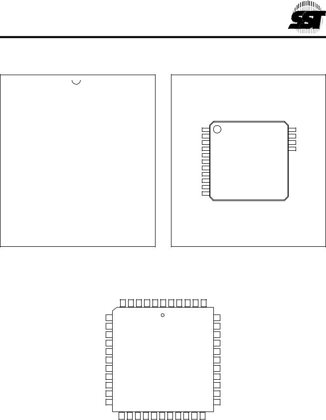
13.0 PACKAGING DIAGRAMS . . . . . . . . . . . . . . . . . . . . . . . . . . . . . . . . . . . . . . . . . . . . . . . . . . . . . . . . . . . . . . 61
©2001 Silicon Storage Technology, Inc. |
S71207-00-000 9/01 555 |
3

FlashFlex51 MCU
SST89E564RD / SST89V564RD / SST89E554RC / SST89V554RC
Preliminary Specifications
LIST OF FIGURES
FIGURE 2-1: Pin Assignments for 40-pin PDIP . . . . . . . . . . . . . . . . . . . . . . . . . . . . . . . . . . . . . . . . . . . . . . . 7 FIGURE 2-2: Pin Assignments for 44-lead TQFP . . . . . . . . . . . . . . . . . . . . . . . . . . . . . . . . . . . . . . . . . . . . . 7 FIGURE 2-3: Pin Assignments for 44-lead PLCC . . . . . . . . . . . . . . . . . . . . . . . . . . . . . . . . . . . . . . . . . . . . . 7 FIGURE 3-1: Program Memory Organization for SST89E564RD and SST89V564RD . . . . . . . . . . . . . . . . 10 FIGURE 3-2: Program Memory Organization for SST89E554RC and SST89V554RC . . . . . . . . . . . . . . . . 11 FIGURE 4-1: I/O Pin Assignments for External Host Mode . . . . . . . . . . . . . . . . . . . . . . . . . . . . . . . . . . . . . 28 FIGURE 4-2: Read-ID . . . . . . . . . . . . . . . . . . . . . . . . . . . . . . . . . . . . . . . . . . . . . . . . . . . . . . . . . . . . . . . . . 31 FIGURE 4-3: Select-Block1 / Select-Block0. . . . . . . . . . . . . . . . . . . . . . . . . . . . . . . . . . . . . . . . . . . . . . . . . 31 FIGURE 4-4: Chip-Erase . . . . . . . . . . . . . . . . . . . . . . . . . . . . . . . . . . . . . . . . . . . . . . . . . . . . . . . . . . . . . . . 32 FIGURE 4-5: Block-Erase for SST89E564RD/SST89V564RD . . . . . . . . . . . . . . . . . . . . . . . . . . . . . . . . . . 32 FIGURE 4-6: Block-Erase for SST89E554RC/SST89V554RC . . . . . . . . . . . . . . . . . . . . . . . . . . . . . . . . . . 33 FIGURE 4-7: Sector-Erase. . . . . . . . . . . . . . . . . . . . . . . . . . . . . . . . . . . . . . . . . . . . . . . . . . . . . . . . . . . . . . 33 FIGURE 4-8: Byte-Program . . . . . . . . . . . . . . . . . . . . . . . . . . . . . . . . . . . . . . . . . . . . . . . . . . . . . . . . . . . . . 34 FIGURE 4-9: Prog-SB1 / Prog-SB2 / Prog-SB3 . . . . . . . . . . . . . . . . . . . . . . . . . . . . . . . . . . . . . . . . . . . . . . 34 FIGURE 4-10: Prog-SC0 / Prog-SC1 . . . . . . . . . . . . . . . . . . . . . . . . . . . . . . . . . . . . . . . . . . . . . . . . . . . . . . 35 FIGURE 4-11: Byte-Verify . . . . . . . . . . . . . . . . . . . . . . . . . . . . . . . . . . . . . . . . . . . . . . . . . . . . . . . . . . . . . . 35 FIGURE 6-1: SPI Master-slave Interconnection. . . . . . . . . . . . . . . . . . . . . . . . . . . . . . . . . . . . . . . . . . . . . . 40 FIGURE 6-2: SPI Transfer Format with CPHA = 0. . . . . . . . . . . . . . . . . . . . . . . . . . . . . . . . . . . . . . . . . . . . 41 FIGURE 6-3: SPI Transfer Format with CPHA = 1. . . . . . . . . . . . . . . . . . . . . . . . . . . . . . . . . . . . . . . . . . . . 41 FIGURE 7-1: Block Diagram of Programmable Watchdog Timer . . . . . . . . . . . . . . . . . . . . . . . . . . . . . . . . 42 FIGURE 9-1: Security Lock Levels. . . . . . . . . . . . . . . . . . . . . . . . . . . . . . . . . . . . . . . . . . . . . . . . . . . . . . . . 45 FIGURE 10-1: Power-on Reset Circuit. . . . . . . . . . . . . . . . . . . . . . . . . . . . . . . . . . . . . . . . . . . . . . . . . . . . . 47 FIGURE 10-2: Oscillator Characteristics . . . . . . . . . . . . . . . . . . . . . . . . . . . . . . . . . . . . . . . . . . . . . . . . . . . 50 FIGURE 11-1: IDD Test Condition, Active Mode . . . . . . . . . . . . . . . . . . . . . . . . . . . . . . . . . . . . . . . . . . . . . . 54 FIGURE 11-2: IDD Test Condition, Idle Mode . . . . . . . . . . . . . . . . . . . . . . . . . . . . . . . . . . . . . . . . . . . . . . . . 54 FIGURE 11-3: IDD Test Condition, Power-Down Mode . . . . . . . . . . . . . . . . . . . . . . . . . . . . . . . . . . . . . . . . 54 FIGURE 11-4: IDD Test Condition, Standby (Stop Clock) Mode. . . . . . . . . . . . . . . . . . . . . . . . . . . . . . . . . . 54 FIGURE 11-5: AC Testing Input/Output, Float Waveform . . . . . . . . . . . . . . . . . . . . . . . . . . . . . . . . . . . . . . 56 FIGURE 11-6: External Program Memory Read Cycle . . . . . . . . . . . . . . . . . . . . . . . . . . . . . . . . . . . . . . . . 57 FIGURE 11-7: External Data Memory Read Cycle . . . . . . . . . . . . . . . . . . . . . . . . . . . . . . . . . . . . . . . . . . . 57 FIGURE 11-8: External Data Memory Write Cycle. . . . . . . . . . . . . . . . . . . . . . . . . . . . . . . . . . . . . . . . . . . . 58 FIGURE 11-9: External Clock Drive Waveform . . . . . . . . . . . . . . . . . . . . . . . . . . . . . . . . . . . . . . . . . . . . . . 58 FIGURE 11-10: Shift Register Mode Timing Waveforms . . . . . . . . . . . . . . . . . . . . . . . . . . . . . . . . . . . . . . . 59
©2001 Silicon Storage Technology, Inc. |
S71207-00-000 9/01 555 |
4

FlashFlex51 MCU
SST89E564RD / SST89V564RD / SST89E554RC / SST89V554RC
Preliminary Specifications
LIST OF TABLES
TABLE |
2-1: Pin Descriptions . . . . . . . . . . . . . . . . . . . . . . . . . . . . . . . . . . . . . . . . . . . . . . . . . . . . . . . . . . . |
. 8 |
TABLE |
3-1: SFCF Values for Program Memory Block Switching for SST89E564RD/SST89V564RD . . . |
11 |
TABLE |
3-2: SFCF Values for Program Memory Block Switching for SST89E554RC/SST89V554RC . . . |
12 |
TABLE |
3-3: SFCF Values Under Different Reset Conditions. . . . . . . . . . . . . . . . . . . . . . . . . . . . . . . . . . . |
12 |
TABLE |
3-4: FlashFlex51 SFR Memory Map . . . . . . . . . . . . . . . . . . . . . . . . . . . . . . . . . . . . . . . . . . . . . . . |
13 |
TABLE |
3-5: CPU related SFRs . . . . . . . . . . . . . . . . . . . . . . . . . . . . . . . . . . . . . . . . . . . . . . . . . . . . . . . . . |
14 |
TABLE |
3-6: Flash Memory Programming SFRs . . . . . . . . . . . . . . . . . . . . . . . . . . . . . . . . . . . . . . . . . . . . |
14 |
TABLE |
3-7: Watchdog Timer SFRs . . . . . . . . . . . . . . . . . . . . . . . . . . . . . . . . . . . . . . . . . . . . . . . . . . . . . . |
15 |
TABLE |
3-8: Timer/Counters SFRs . . . . . . . . . . . . . . . . . . . . . . . . . . . . . . . . . . . . . . . . . . . . . . . . . . . . . . . |
15 |
TABLE |
3-9: Interface SFRs . . . . . . . . . . . . . . . . . . . . . . . . . . . . . . . . . . . . . . . . . . . . . . . . . . . . . . . . . . . . |
16 |
TABLE |
3-10: PCA SFRs . . . . . . . . . . . . . . . . . . . . . . . . . . . . . . . . . . . . . . . . . . . . . . . . . . . . . . . . . . . . . . |
16 |
TABLE |
3-11: PCA Module Modes . . . . . . . . . . . . . . . . . . . . . . . . . . . . . . . . . . . . . . . . . . . . . . . . . . . . . . . |
22 |
TABLE |
4-1: External Host Mode Commands for SST89E564RD/SST89V564RD . . . . . . . . . . . . . . . . . . |
27 |
TABLE |
4-2: External Host Mode Commands for SST89E554RC/SST89V554RC . . . . . . . . . . . . . . . . . . |
28 |
TABLE |
4-3: Signature Bytes . . . . . . . . . . . . . . . . . . . . . . . . . . . . . . . . . . . . . . . . . . . . . . . . . . . . . . . . . . . |
29 |
TABLE |
4-4: IAP Address Resolution for SST89E564RD/SST89V564RD . . . . . . . . . . . . . . . . . . . . . . . . . |
36 |
TABLE |
4-5: In-Application Programming Mode Commands for SST89E564RD/SST89V564RD . . . . . . . |
38 |
TABLE |
4-6: In-Application Programming Mode Commands for SST89E554RC/SST89V554RC . . . . . . . |
38 |
TABLE |
4-7: Flash Memory Programming/Verification Parameters . . . . . . . . . . . . . . . . . . . . . . . . . . . . . . |
39 |
TABLE |
8-1: Count Pulse Selected Bits . . . . . . . . . . . . . . . . . . . . . . . . . . . . . . . . . . . . . . . . . . . . . . . . . . . |
43 |
TABLE |
8-2: Possible Modes and Associated Values for CCAPMn . . . . . . . . . . . . . . . . . . . . . . . . . . . . . . |
43 |
TABLE |
9-1: Security Lock Options. . . . . . . . . . . . . . . . . . . . . . . . . . . . . . . . . . . . . . . . . . . . . . . . . . . . . . . |
45 |
TABLE |
9-2: Security Lock Access Table . . . . . . . . . . . . . . . . . . . . . . . . . . . . . . . . . . . . . . . . . . . . . . . . . . |
46 |
TABLE |
10-1: Interrupt Polling Sequence . . . . . . . . . . . . . . . . . . . . . . . . . . . . . . . . . . . . . . . . . . . . . . . . . . |
48 |
TABLE |
10-2: Power Saving Modes . . . . . . . . . . . . . . . . . . . . . . . . . . . . . . . . . . . . . . . . . . . . . . . . . . . . . . |
49 |
TABLE |
11-1: Operating Range . . . . . . . . . . . . . . . . . . . . . . . . . . . . . . . . . . . . . . . . . . . . . . . . . . . . . . . . . |
51 |
TABLE |
11-2: Reliability Characteristics . . . . . . . . . . . . . . . . . . . . . . . . . . . . . . . . . . . . . . . . . . . . . . . . . . . |
51 |
TABLE |
11-3: DC Electrical Characteristics: 40MHz devices; 4.5-5.5V . . . . . . . . . . . . . . . . . . . . . . . . . . . |
52 |
TABLE |
11-4: DC Electrical Characteristics: 25MHz devices; 2.7-3.6V . . . . . . . . . . . . . . . . . . . . . . . . . . . |
53 |
TABLE |
11-5: AC Electrical Characteristics . . . . . . . . . . . . . . . . . . . . . . . . . . . . . . . . . . . . . . . . . . . . . . . . |
55 |
TABLE |
11-6: External Clock Drive . . . . . . . . . . . . . . . . . . . . . . . . . . . . . . . . . . . . . . . . . . . . . . . . . . . . . . . |
58 |
TABLE |
11-7: Serial Port Timing . . . . . . . . . . . . . . . . . . . . . . . . . . . . . . . . . . . . . . . . . . . . . . . . . . . . . . . . . |
59 |
©2001 Silicon Storage Technology, Inc. |
S71207-00-000 9/01 555 |
5

FlashFlex51 MCU
SST89E564RD / SST89V564RD / SST89E554RC / SST89V554RC
Preliminary Specifications
1.0 FUNCTIONAL BLOCKS
FUNCTIONAL BLOCK DIAGRAM
Watchdog Timer
Interrupt
Control
8051 |
|
|
|
|
|
|
|
||||||||||||
|
|
|
|
|
|
|
CPU Core |
|
|
|
|
|
|
||||||
|
|
|
|
|
|
|
|
|
|
|
|
|
|
|
|
|
|
|
|
|
SuperFlash |
|
|
|
|
|
|
|
|
|
|
|
|
|
|
|
|
|
|
|
EEPROM |
|
|
|
|
|
|
|
|
|
|
|
|
|
|
|
|
|
|
|
Primary |
|
|
|
|
|
|
|
|
|
|
|
|
|
|
|
|
|
|
|
Block |
|
|
|
|
|
|
|
|
|
|
|
|
|
|
|
|
|
|
|
32K/64K x81 |
|
|
|
|
|
|
|
|
|
|
|
|
|
|
RAM |
|
|
|
|
|
|
|
|
|
|
|
|
|
|
|
|
|
|
|
1K x8 |
|
|
|
|
Secondary |
|
|
|
|
|
|
|
|
|
|
|
|
|
|
|
|
||
|
|
|
|
|
|
|
|
|
|
|
|
|
|
|
|
|
|
|
|
|
|
|
|
|
|
|
|
|
|
|
|
|
|
|
|
|
|
||
|
Block |
|
|
|
|
|
|
|
|
|
|
|
|
|
|
|
|
|
I/O |
|
8K x8 |
|
|
|
|
|
|
|
|
|
|
|
|
I/O Port 0 |
|
|
|||
|
|
|
|
|
|
|
|
|
|
|
|
|
|
|
|||||
|
|
|
|
|
|
|
|
|
|
|
|
|
|
|
|
|
|
8 |
|
|
|
|
|
|
|
|
|
|
|
|
|
|
|
|
|
|
|
||
|
|
|
|
|
|
|
|
|
|
|
|
|
|
|
|
|
|
||
|
|
|
|
Security |
|
|
|
|
I/O Port 1 |
|
|
I/O |
|||||||
|
|
|
|
|
|
|
|
|
|
||||||||||
|
|
|
|
Lock |
|
|
|
|
|
|
|
|
8 |
||||||
|
|
|
|
|
|
|
|
|
|
|
|
|
|
|
|
|
|
||
|
|
|
|
|
|
|
|
|
|
|
|
|
|
I/O Port 2 |
|
|
I/O |
||
|
|
|
|
|
|
|
|
|
|
|
|
|
|
|
|
||||
|
|
|
|
|
|
|
|
|
|
|
|
8 |
|||||||
|
Timer 0 (16-bits) |
|
|
|
|
|
|
|
|
|
|||||||||
|
|
|
|
|
|
|
|
|
|
||||||||||
|
|
|
|
|
|
|
|
|
|
|
|
|
|
I/O Port 3 |
|
|
I/O |
||
|
|
|
|
|
|
|
|
|
|
|
|
|
|
|
|
||||
|
|
|
|
|
|
|
|
|
|
|
|
|
|
||||||
|
Timer 1 (16-bits) |
|
|
|
|
|
|
|
|
|
|
|
|||||||
|
|
|
|
|
|
|
|
|
|
|
|
||||||||
|
|
|
|
|
|
|
|
|
|
|
|
|
|
|
|
SPI |
|
|
|
|
|
|
|
|
|
|
|
|
|
|
|
|
|
|
|
|
|
|
|
|
|
|
|
|
|
|
|
|
|
|
|
|
|
|
|
|
|
|
|
Timer 2 (16-bits)
8-bit PCA 
 Enhanced
UART
1.64K x8 for SST89E564RD and SST89V564RD
32K x8 for SST89E554RC and SST89V554RC
9 Interrupts
555 ILL B1.0
©2001 Silicon Storage Technology, Inc. |
S71207-00-000 9/01 555 |
6
FlashFlex51 MCU
SST89E564RD / SST89V564RD / SST89E554RC / SST89V554RC
Preliminary Specifications
2.0 PIN ASSIGNMENTS
(T2) |
P1.0 |
|
1 |
40 |
|
VDD |
|
|
|
|
|||||
|
|
|
39 |
|
P0.0 |
(AD0) |
|
(T2 Ex) P1.1 |
|
2 |
|
||||
|
|
|
|
38 |
|
P0.1 |
(AD1) |
|
P1.2 |
|
3 |
|
|||
|
|
|
|
37 |
|
P0.2 |
(AD2) |
|
P1.3 |
|
4 |
|
|||
|
|
|
36 |
|
P0.3 |
(AD3) |
|
(SS#) P1.4 |
|
5 |
|
||||
|
|
|
35 |
|
P0.4 |
(AD4) |
|
(MOSI) P1.5 |
|
6 |
|
||||
|
|
|
40-pin PDIP 34 |
|
P0.5 |
(AD5) |
|
(MISO) P1.6 |
|
7 |
|
||||
|
|
|
|
|
|
|
|
(SCK) P1.7 |
|
8 |
Top View 33 |
|
P0.6 |
(AD6) |
|
|
|
|
|
32 |
|
P0.7 |
(AD7) |
|
RST |
|
9 |
|
|||
|
|
|
31 |
|
EA# |
|
|
(RXD) P3.0 |
|
10 |
|
|
|||
|
|
|
30 |
|
ALE/PROG# |
||
(TXD) P3.1 |
|
11 |
|
||||
|
|
|
29 |
|
PSEN# |
||
(INT0#) P3.2 |
|
12 |
|
||||
|
|
|
28 |
|
P2.7 |
(A15) |
|
(INT1#) P3.3 |
|
13 |
|
||||
|
|
|
27 |
|
P2.6 |
(A14) |
|
(T0) P3.4 |
|
14 |
|
||||
|
|
|
26 |
|
P2.5 |
(A13) |
|
(T1) P3.5 |
|
15 |
|
||||
|
|
|
25 |
|
P2.4 |
(A12) |
|
(WR#) P3.6 |
|
16 |
|
||||
|
|
|
24 |
|
P2.3 |
(A11) |
|
(RD#) P3.7 |
|
17 |
|
||||
|
|
|
23 |
|
P2.2 |
(A10) |
|
XTAL2 |
|
18 |
|
||||
|
|
|
22 |
|
P2.1 |
(A9) |
|
XTAL1 |
|
19 |
|
||||
|
|
|
|
21 |
|
P2.0 |
(A8) |
|
VSS |
|
20 |
|
|||
|
|
|
|
|
|
|
|
555 ILL F1a.0
|
|
|
P1.4(SS#) |
|
P1.3 |
|
P1.2 |
|
P1.1(T2 Ex) |
|
P1.0(T2) |
|
Reserved |
|
V |
|
P0.0(AD0) |
|
P0.1(AD1) |
|
P0.2(AD2) |
|
P0.3(AD3) |
|
|
|
||
|
|
|
|
|
|
|
|
|
|
|
|
|
|
|
DD |
|
|
|
|
|
|
|
|
|
|
|
|
|
|
|
|
|
|
|
|
|
|
|
|
|
|
|
|
|
|
|
|
|
|
|
|
|
|
|
|
|
|
|
|
44 |
43 |
42 |
41 |
40 |
39 |
38 |
|
37 |
36 |
35 |
34 |
|
|
|
|
|||||||||||
(MOSI) P1.5 |
1 |
|
|
|
|
|
|
|
|
|
|
|
|
|
|
|
|
|
|
|
|
33 |
|
P0.4 |
(AD4) |
|||
(MISO) P1.6 |
2 |
|
|
|
|
|
|
|
|
|
|
|
|
|
|
|
|
|
|
|
|
32 |
|
P0.5 |
(AD5) |
|||
(SCK) P1.7 |
3 |
|
|
|
|
|
|
|
|
|
|
|
|
|
|
|
|
|
|
|
|
31 |
|
P0.6 |
(AD6) |
|||
|
RST |
4 |
|
|
|
|
|
|
|
|
|
|
|
|
|
|
|
|
|
|
|
|
30 |
|
P0.7 |
(AD7) |
||
(RXD) P3.0 |
5 |
|
|
|
|
|
44-lead TQFP |
|
|
|
|
29 |
|
EA# |
|
|||||||||||||
|
|
|
|
|
|
|
|
|
|
|||||||||||||||||||
Reserved |
6 |
|
|
|
|
|
|
|
|
|
28 |
|
Reserved |
|||||||||||||||
(TXD) P3.1 |
7 |
|
|
|
|
|
|
|
Top View |
|
|
|
|
|
|
27 |
|
ALE/PROG# |
||||||||||
(INT0#) P3.2 |
8 |
|
|
|
|
|
|
|
|
|
|
|
|
|
|
|
|
|
|
|
|
26 |
|
PSEN# |
||||
|
|
|
|
|
|
|
|
|
|
|
|
|
|
|
|
|
|
|
|
|||||||||
(INT1#) P3.3 |
9 |
|
|
|
|
|
|
|
|
|
|
|
|
|
|
|
|
|
|
|
|
25 |
|
P2.7 |
(A15) |
|||
|
|
|
|
|
|
|
|
|
|
|
|
|
|
|
|
|
|
|
|
|||||||||
(T0) P3.4 |
10 |
|
|
|
|
|
|
|
|
|
|
|
|
|
|
|
|
|
|
|
|
24 |
|
P2.6 |
(A14) |
|||
|
|
|
|
|
|
|
|
|
|
|
|
|
|
|
|
|
|
|
|
|||||||||
(T1) |
P3.5 |
11 |
|
|
|
|
|
|
|
|
|
|
|
|
|
|
|
|
|
|
|
|
23 |
|
P2.5 |
(A13) |
||
|
|
|
|
|
|
|
|
|
|
|
|
|
|
|
|
|
|
|
|
|||||||||
|
|
12 |
13 |
14 |
15 |
16 |
17 |
18 |
|
19 |
20 |
21 |
22 |
|
|
|
|
|||||||||||
|
|
|
|
|
|
|
|
|
|
|
|
|
|
|
|
|
|
|
|
|
|
|
|
|
|
|
||
|
|
|
|
|
|
|
|
|
|
|
|
|
|
|
|
|
|
|
|
|
|
|
|
|
|
|
|
|
|
|
|
(WR#)P3.6 |
|
(RD#)P3.7 |
|
XTAL2 |
|
XTAL1 |
|
V |
|
Reserved |
|
(A8)P2.0 |
|
(A9)P2.1 |
|
(A10)P2.2 |
|
(A11)P2.3 |
|
(A12)P2.4 |
|
|
|
||
|
|
|
|
|
|
|
|
|
|
|
SS |
|
|
|
|
|
|
|
|
|
|
|
|
|
|
|
|
|
555 ILL F1b.0
FIGURE |
2-1: PIN ASSIGNMENTS FOR 40-PIN PDIP |
|
|
|
FIGURE |
2-2: PIN ASSIGNMENTS FOR 44-LEAD TQFP |
||||||||
|
|
|
|
|
|
|
|
|
|
|
|
|
|
|
|
|
P1.4(SS#) |
P1.3 |
P1.2 |
P1.1(T2 Ex) |
P1.0(T2) |
Reserved |
V |
P0.0(AD0) |
P0.1(AD1) |
P0.2(AD2) |
P0.3(AD3) |
|
|
|
|
|
|
|
|
|
|
DD |
|
|
|
|
|
|
|
|
6 |
5 |
4 |
3 |
2 |
1 |
44 |
43 |
42 |
41 |
40 |
|
|
|
(MOSI) P1.5 |
7 |
|
|
|
|
|
|
|
|
|
39 |
P0.4 |
(AD4) |
|
(MISO) P1.6 |
8 |
|
|
|
|
|
|
|
|
|
38 |
P0.5 |
(AD5) |
|
(SCK) P1.7 |
9 |
|
|
|
|
|
|
|
|
|
37 |
P0.6 |
(AD6) |
|
RST |
10 |
|
|
|
|
|
|
|
|
|
36 |
P0.7 |
(AD7) |
|
(RXD) P3.0 |
11 |
|
|
44-lead PLCC |
|
|
35 |
EA# |
|
||||
|
Reserved |
12 |
|
|
|
Top View |
|
|
|
34 |
Reserved |
|||
|
(TXD) P3.1 |
13 |
|
|
|
|
|
|
|
|
|
33 |
ALE/PROG# |
|
|
(INT0#) P3.2 |
14 |
|
|
|
|
|
|
|
|
|
32 |
PSEN# |
|
|
(INT1#) P3.3 |
15 |
|
|
|
|
|
|
|
|
|
31 |
P2.7 |
(A15) |
|
(T0) P3.4 |
16 |
|
|
|
|
|
|
|
|
|
30 |
P2.6 |
(A14) |
|
(T1) P3.5 |
17 |
|
|
|
|
|
|
|
|
|
29 |
P2.5 |
(A13) |
|
|
18 |
19 |
20 |
21 |
22 |
23 |
24 |
25 |
26 |
27 |
28 |
|
|
|
|
(WR#)P3.6 |
(RD#)P3.7 |
XTAL2 |
XTAL1 |
SS |
Reserved |
(A8)P2.0 |
(A9)P2.1 |
(A10)P2.2 |
(A11)P2.3 |
(A12)P2.4 |
|
|
|
|
V |
|
|
||||||||||
|
|
|
|
|
|
|
|
|
|
|
|
555 ILL F01c.0 |
|
|
|
|
|
|
|
|
|
|
|
||||||
FIGURE |
2-3: PIN ASSIGNMENTS FOR 44-LEAD PLCC |
|
|
|
|
|
|
|
||||||
|
|
|
|
|
|
|
|
|
|
|
|
|
|
|
©2001 Silicon Storage Technology, Inc. |
|
|
|
|
|
|
|
|
|
|
|
|
S71207-00-000 9/01 555 |
|
7

FlashFlex51 MCU
SST89E564RD / SST89V564RD / SST89E554RC / SST89V554RC
|
|
|
Preliminary Specifications |
2.1 Pin Descriptions |
|
||
TABLE |
2-1: PIN DESCRIPTIONS (1 OF 2) |
||
|
|
|
|
Symbol |
|
Type1 |
Name and Functions |
P0[7:0] |
|
I/O |
Port 0: Port 0 is an 8-bit open drain bi-directional I/O port. As an output port each pin can |
|
|
|
sink several LS TTL inputs. Port 0 pins float that have “1”s written to them, and in this state |
|
|
|
can be used as high-impedance inputs. Port 0 is also the multiplexed low-order address and |
|
|
|
data bus during accesses to external memory. In this application, it uses strong internal pull- |
|
|
|
ups when transitioning to VOH. Port 0 also receives the code bytes during the external host |
|
|
|
mode programming, and outputs the code bytes during the external host mode verification. |
|
|
|
External pull-ups are required during program verification. |
|
|
|
|
P1[7:0] |
|
I/O with internal |
Port 1: Port 1 is an 8-bit bi-directional I/O port with internal pull-ups. The Port 1 output buffers |
|
|
pull-ups |
can drive LS TTL inputs. Port 1 pins are pulled high by the internal pull-ups when “1”s are |
|
|
|
written to them and can be used as inputs in this state. As inputs, Port 1 pins that are exter- |
|
|
|
nally pulled low will source current (IIL, see Tables 11-3 and 11-4) because of the internal pull- |
|
|
|
ups. P1[5, 6, 7] have high current drive of 16 mA. Port 1 also receives the low-order address |
|
|
|
bytes during the external host mode programming and verification. |
|
|
|
|
P1[0] |
|
I/O |
T2: External count input to Timer/Counter 2 or Clock-out from Timer/Counter 2 |
|
|
|
|
P1[1] |
|
I |
T2EX: Timer/Counter 2 capture/reload trigger and direction control |
|
|
|
|
P1[2] |
|
I |
ECI: PCA Timer/Counter External Input: |
|
|
|
This signal is the external clock input for the PCS timer/counter. |
|
|
|
|
P1[3] |
|
I/O |
CEX0: Compare/Capture Module External I/O |
|
|
|
Each compare/capture module connects to a Port 1 pin for external I/O. When not used by |
|
|
|
the PCA, this pin can handle standard I/O. |
|
|
|
|
P1[4] |
|
I/O |
SS#: Master Input or Slave Output for SPI. |
|
|
|
OR |
|
|
|
CEX1: Compare/Capture Module External I/O |
|
|
|
|
P1[5] |
|
I/O |
MOSI: Master Output line, Slave Input line for SPI |
|
|
|
OR |
|
|
|
CEX2: Compare/Capture Module External I/O |
|
|
|
|
P1[6] |
|
I/O |
MISO: Master Input line, Slave Output line for SPI |
|
|
|
OR |
|
|
|
CEX3: Compare/Capture Module External I/O |
|
|
|
|
P1[7] |
|
I/O |
SCK: Master clock output, slave clock input line for SPI |
|
|
|
OR |
|
|
|
CEX4: Compare/Capture Module External I/O |
|
|
|
|
P2[7:0] |
|
I/O with internal |
Port 2: Port 2 is an 8-bit bi-directional I/O port with internal pull-ups. Port 2 pins are pulled |
|
|
pull-ups |
high by the internal pull-ups when “1”s are written to them and can be used as inputs in this |
|
|
|
state. As inputs, Port 2 pins that are externally pulled low will source current (IIL, see Tables |
|
|
|
11-3 and 11-4) because of the internal pull-ups. Port 2 sends the high-order address byte |
|
|
|
during fetches from external Program memory and during accesses to external Data Memory |
|
|
|
that use 16-bit address (MOVX@DPTR). In this application, it uses strong internal pull-ups |
|
|
|
when transitioning to VOH. Port 2 also receives some control signals and a partial of high- |
|
|
|
order address bits during the external host mode programming and verification. |
|
|
|
|
P3[7:0] |
|
I/O with internal |
Port 3: Port 3 is an 8-bit bidirectional I/O port with internal pull-ups. The Port 3 output buffers |
|
|
pull-ups |
can drive LS TTL inputs. Port 3 pins are pulled high by the internal pull-ups when “1”s are |
|
|
|
written to them and can be used as inputs in this state. As inputs, Port 3 pins that are exter- |
|
|
|
nally pulled low will source current (IIL, see Tables 11-3 and 11-4) because of the internal pull- |
|
|
|
ups. Port 3 also receives some control signals and a partial of high-order address bits during |
|
|
|
the external host mode programming and verification. |
|
|
|
|
P3[0] |
|
I |
RXD: Serial input line |
|
|
|
|
P3[1] |
|
O |
TXD: Serial output line |
|
|
|
|
P3[2] |
|
I |
INT0#: External Interrupt 0 Input |
|
|
|
|
|
|
|
|
©2001 Silicon Storage Technology, Inc. |
S71207-00-000 9/01 555 |
||
|
|
|
8 |

FlashFlex51 MCU
SST89E564RD / SST89V564RD / SST89E554RC / SST89V554RC
Preliminary Specifications
TABLE 2-1: PIN DESCRIPTIONS (CONTINUED) (2 OF 2)
Symbol |
Type1 |
Name and Functions |
P3[3] |
I |
INT1#: External Interrupt 1 Input |
|
|
|
P3[4] |
I |
T0: External count input to Timer/Counter 0 |
|
|
|
P3[5] |
I |
T1: External count input to Timer/Counter 1 |
|
|
|
P3[6] |
O |
WR#: External Data Memory Write strobe |
|
|
|
P3[7] |
O |
RD#: External Data Memory Read strobe |
|
|
|
PSEN# |
I/O |
Program Store Enable: PSEN# is the Read strobe to External Program Store. When the |
|
|
device is executing from Internal Program Memory, PSEN# is inactive (VOH). When the |
|
|
device is executing code from External Program Memory, PSEN# is activated twice each |
|
|
machine cycle, except when access to External Data Memory while one PSEN# activation is |
|
|
skipped in each machine cycle. A forced high-to-low input transition on the PSEN# pin while |
|
|
the RST input is continually held high for more than ten machine cycles will cause the device |
|
|
to enter External Host mode for programming. |
|
|
|
RST |
I |
Reset: While the oscillator is running, a high logic state on this pin for two machine cycles will |
|
|
reset the device. After a reset, if the PSEN# pin is driven by a high-to-low input transition |
|
|
while the RST input pin is held high, the device will enter the External Host mode, otherwise |
|
|
the device will enter the Normal operation mode. |
|
|
|
EA# |
I |
External Access Enable: EA# must be driven to VIL in order to enable the device to fetch |
|
|
code from the External Program Memory. EA# must be driven to VIH for internal program exe- |
|
|
cution. However, Security lock level 4 will disable EA#, and program execution is only possi- |
|
|
ble from internal program memory. The EA# pin can tolerate a high voltage2 of 12V |
|
|
(see “Absolute Maximum Stress Ratings” on page 51). |
|
|
|
ALE/PROG# |
I/O |
Address Latch Enable: ALE is the output signal for latching the low byte of the address dur- |
|
|
ing accesses to external memory. This pin is also the programming pulse input (PROG#) for |
|
|
the external host mode. ALE is activated twice each machine cycle, except when access to |
|
|
External Data Memory, one ALE activation is skipped in the second machine cycle. However, |
|
|
if AO is set to 1, ALE is disabled. (see “Auxiliary Register (AUXR)” on page 20) |
|
|
|
XTAL1 |
I |
Oscillator: Input and output to the inverting oscillator amplifier. XTAL1 is input to internal |
XTAL2 |
O |
clock generation circuits from an external clock source. |
|
|
|
VDD |
I |
Power Supply: Supply voltage during normal, Idle, Power Down, and Standby Mode opera- |
|
|
tions. |
|
|
|
VSS |
I |
Ground: Circuit ground. (0V reference) |
|
|
T2-1.0 555 |
1.I = Input; O = Output
2.It is not necessary to receive a 12V programming supply voltage during flash programming.
©2001 Silicon Storage Technology, Inc. |
S71207-00-000 9/01 555 |
9

FlashFlex51 MCU
SST89E564RD / SST89V564RD / SST89E554RC / SST89V554RC
3.0 MEMORY ORGANIZATION
The device has separate address spaces for program and data memory.
3.1 Program Memory
There are two internal flash memory blocks in the device. The primary flash memory block (Block 0) has 64/32 KByte. The secondary flash memory block (Block 1) has 8 KByte. Since the total program address space is limited to 64/32 KByte, the SFCF[1:0] bit are used to control Program
Preliminary Specifications
Bank Selection. Please refer to Figure 3-1 and Figure 3-2 for the program memory configurations. Program Bank Select is described in the next section.
The 64K/32K x8 primary SuperFlash block is organized as 512/256 sectors, each sector consists of 128 Bytes.
The 8K x8 secondary SuperFlash block is organized as 64 sectors, each sector consists also of 128 Bytes.
For both blocks, the 7 least significant program address bits select the byte within the sector. The remainder of the program address bits select the sector within the block.
|
EA# = 0 |
|
EA# = 1 |
|
EA# = 1 |
|
|
|
SFCF[1:0] = 00 |
SFCF[1:0] = 01, 10, 11 |
|||
|
|
|
||||
FFFFH |
|
FFFFH |
|
FFFFH |
|
|
|
56 KByte |
|
|
|||
|
|
|
|
|
|
|
|
|
|
Block 0 |
|
|
|
|
External |
|
|
|
64 KByte |
|
|
64 KByte |
|
|
|
Block 0 |
|
|
|
2000H |
|
|
|
|
|
|
1FFFH |
|
|
|
|
|
|
8 KByte |
|
|
|
|
|
|
|
|
|
|
|
|
|
|
Block 1 |
|
|
|
0000H |
|
0000H |
|
0000H |
|
|
|
|
|
|
|
555 ILL F02.0 |
|
FIGURE 3-1: PROGRAM MEMORY ORGANIZATION FOR SST89E564RD AND SST89V564RD
©2001 Silicon Storage Technology, Inc. |
S71207-00-000 9/01 555 |
10
FlashFlex51 MCU
SST89E564RD / SST89V564RD / SST89E554RC / SST89V554RC
Preliminary Specifications
|
EA# = 0 |
|
|
EA# = 1 |
EA# = 1 |
|
|
EA# = 1 |
||
|
|
|
SFCF[1:0] = 00 |
SFCF[1:0] = 01 |
SFCF[1:0] = 10, 11 |
|||||
|
|
|
|
|||||||
FFFFH |
|
FFFFH |
|
FFFFH |
|
FFFFH |
|
|
||
|
8 KByte |
8 KByte |
|
|
||||||
|
|
|
|
|
|
|
|
|
||
|
|
|
|
Block 1 |
|
Block 1 |
|
|
|
|
|
|
E000H |
|
E000H |
|
|
|
External |
|
|
|
|
|
|
|
|
|||||
|
|
DFFFH |
|
DFFFH |
|
|
|
32 KByte |
|
|
|
|
External |
External |
|
|
|||||
|
|
|
|
|
|
|
|
|
||
|
|
|
|
24 KByte |
|
24 KByte |
|
|
|
|
|
External |
8000H |
|
8000H |
|
8000H |
|
|
||
|
64 KByte |
|
|
|
|
|||||
|
7FFFH |
|
7FFFH |
|
7FFFH |
|
|
|
||
|
|
|
|
|
|
|
||||
|
|
|
|
24 KByte |
|
|
|
|
|
|
|
|
|
|
Block 0 |
|
|
|
|
|
|
|
|
2000H |
|
|
32 KByte |
|
|
32 KByte |
|
|
|
|
|
|
|
|
|
|
|
||
|
|
1FFFH |
|
|
|
Block 0 |
|
|
Block 0 |
|
|
|
|
|
|
|
|
|
|||
|
|
|
|
|
|
|
|
|
|
|
|
|
|
|
8 KByte |
|
|
|
|
|
|
|
|
|
|
Block 1 |
|
|
|
|
|
|
0000H |
|
0000H |
|
|
0000H |
|
0000H |
|
|
|
|
|
|
|
|
|
|
|
|
555 ILL F03.2 |
|
FIGURE 3-2: PROGRAM MEMORY ORGANIZATION FOR SST89E554RC AND SST89V554RC
3.2 Program Memory Block Switching
The program memory block switching feature of the device allows either Block 1 or the lowest 8 KByte of Block 0 to be used for the lowest 8 KByte of the program address space. SFCF[1:0] controls program memory block switching.
TABLE 3-1: SFCF VALUES FOR PROGRAM MEMORY BLOCK SWITCHING FOR SST89E564RD/SST89V564RD
SFCF[1:0] Program Memory Block Switching
01, 10, 11 Block 1 is not visible to the PC;
Block 1 is reachable only via In-Application Programming from 000H - 1FFFH.
00Block 1 is overlaid onto the low 8K of the program address space; occupying address locations 0000H - 1FFFH. When the PC falls within 0000H - 1FFFH, the instruction will be fetched from Block 1 instead of Block 0. Outside of 0000H - 1FFFH, Block 0 is used. Locations 0000H - 1FFFH of Block 0 are reachable through In-Application Programming.
T3-1.0 555
©2001 Silicon Storage Technology, Inc. |
S71207-00-000 9/01 555 |
11

FlashFlex51 MCU
SST89E564RD / SST89V564RD / SST89E554RC / SST89V554RC
Preliminary Specifications
TABLE 3-2: SFCF VALUES FOR PROGRAM MEMORY BLOCK SWITCHING FOR SST89E554RC/SST89V554RC
SFCF[1:0] Program Memory Block Switching
10, 11 Block 1 is not visible to the PC;
Block 1 is reachable only via In-Application Programming from E000H - FFFFH.
01Both Block 0 and Block 1 are visible to the PC.
Block 0 is occupied from 0000H - 7FFFH. Block 1 is occupied from E000H - FFFFH.
00Block 1 is overlaid onto the low 8K of the program address space; occupying address locations 0000H - 1FFFH. When the PC falls within 0000H - 1FFFH, the instruction will be fetched from Block 1 instead of Block 0. Outside of 0000H - 1FFFH, Block 0 is used. Locations 0000H - 1FFFH of Block 0 are reachable through In-Application Programming.
T3-2.0 555
3.2.1 Reset Configuration of Program Memory
Block Switching
Program memory block switching is initialized after reset according to the state of the Start-up Configuration bit SC0. The SC0 bit is programmed via an External Host Mode command or an IAP Mode command. See Table 4-2 and Table 4-6.
Once out of reset, the SFCF[0] bit can be changed dynamically by the program for desired effects. Changing SFCF[0] will not change the SC0 bit.
Caution must be taken when dynamically changing the SFCF[0] bit. Since this will cause different physical memory to be mapped to the logical program address space. The user must avoid executing block switching instructions within the address range 0000H to 1FFFH.
TABLE |
3-3: SFCF VALUES UNDER DIFFERENT |
|||
|
|
RESET CONDITIONS |
|
|
|
|
|
|
|
|
|
State of SFCF[1:0] after: |
||
|
|
|
|
|
|
|
|
WDT |
|
|
|
Power-on |
Reset |
|
|
|
or |
or |
|
SC11 |
|
External |
Brown-out |
Software |
SC0 |
Reset |
Reset |
Reset |
|
1 |
1 |
00 |
x0 |
10 |
|
|
(default) |
|
|
|
|
|
|
|
1 |
0 |
01 |
x1 |
11 |
|
|
|
|
|
0 |
1 |
10 |
10 |
10 |
|
|
|
|
|
0 |
0 |
11 |
11 |
11 |
|
|
|
|
|
|
|
|
|
T3-3.0 555 |
1. SC1 only applies to SST89E554RC and SST89V554RC.
3.3 Data Memory
The device has 1024 x8 bits of on-chip RAM and can address up to 64 KByte of external data memory.
The device has four sections of internal data memory:
1.The lower 128 Bytes of RAM (00H to 7FH) are directly and indirectly addressable.
2.The higher 128 Bytes of RAM (80H to FFH) are indirectly addressable.
3.The Special Function Registers (SFRs, 80H to FFH) are directly addressable only.
4.The expanded RAM of 768 Bytes (00H to 2FFH) is indirectly addressable by the move external instruction (MOVX) and clearing the EXTRAM bit. (See “Auxiliary Register (AUXR)” on page 20)
3.4 Dual Data Pointers
The device has two 16-bit data pointers. The DPTR Select (DPS) bit in AUXR1 determines which of the two data pointers is accessed. When DPS=0, DPTR0 is selected; when DPS=1, DPTR1 is selected. Quickly switching between the two data pointers can be accomplished by a single INC instruction on AUXR1.
3.5 Special Function Registers (SFR)
Most of the unique features of the FlashFlex51 microcontroller family are controlled by bits in special function registers (SFRs) located in the SFR Memory Map shown in Table 3-4. Individual descriptions of each SFR are provided and Reset values indicated in Tables 3-5 to 3-9.
©2001 Silicon Storage Technology, Inc. |
S71207-00-000 9/01 555 |
12

FlashFlex51 MCU
SST89E564RD / SST89V564RD / SST89E554RC / SST89V554RC
Preliminary Specifications
TABLE |
3-4: FLASHFLEX51 SFR MEMORY MAP |
|
|
|
|
|
||||
|
|
|
|
|
8 BYTES |
|
|
|
|
|
|
|
|
|
|
|
|
|
|
|
|
F8H |
|
IPA1 |
CH |
CCAP0H |
CCAP1H |
CCAP2H |
CCAP3H |
CCAP4H |
|
FFH |
F0H |
|
B1 |
|
|
|
|
|
|
IPAH |
F7H |
E8H |
|
IEA1 |
CL |
CCAP0L |
CCAP1L |
CCAP2L |
CCAP3L |
CCAP4L |
|
EFH |
E0H |
|
ACC1 |
|
|
|
|
|
|
|
E7H |
D8H |
|
CCON1 |
CMOD |
CCAPM0 |
CCAPM1 |
CCAPM2 |
CCAPM3 |
CCAPM4 |
|
DFH |
D0H |
|
PSW1 |
|
|
|
|
SPCR |
|
|
D7H |
C8H |
|
T2CON1 |
T2MOD |
RCAP2L |
RCAP2H |
TL2 |
TH2 |
|
|
CFH |
C0H |
|
WDTC1 |
|
|
|
|
|
|
|
C7H |
B8H |
|
IP1 |
SADEN |
|
|
|
|
|
|
BFH |
B0H |
|
P31 |
SFCF |
SFCM |
SFAL |
SFAH |
SFDT |
SFST |
IPH |
B7H |
A8H |
|
IE1 |
SADDR |
SPSR |
|
|
|
|
|
AFH |
A0H |
|
P21 |
|
AUXR1 |
|
|
|
|
|
A7H |
98H |
|
SCON1 |
SBUF |
|
|
|
|
|
|
9FH |
90H |
|
P11 |
|
|
|
|
|
|
|
97H |
88H |
|
TCON1 |
TMOD |
TL0 |
TL1 |
TH0 |
TH1 |
AUXR |
|
8FH |
80H |
|
P01 |
SP |
DPL |
DPH |
|
WDTD |
SPDR |
PCON |
87H |
|
|
|
|
|
|
|
|
|
|
T3-4.1 555 |
1. SFRs are bit addressable.
©2001 Silicon Storage Technology, Inc. |
S71207-00-000 9/01 555 |
13

FlashFlex51 MCU
SST89E564RD / SST89V564RD / SST89E554RC / SST89V554RC
|
|
|
|
|
|
|
|
|
|
|
|
|
|
|
|
|
|
|
|
Preliminary Specifications |
||||
TABLE |
3-5: CPU RELATED SFRS |
|
|
|
|
|
|
|
|
|
|
|
|
|
|
|
|
|
||||||
|
|
|
|
|
|
|
|
|
|
|
|
|
|
|
|
|
|
|
|
|
|
|
|
|
|
|
|
|
Direct |
|
|
Bit Address, Symbol, or Alternative Port Function |
|
|
|
RESET |
|||||||||||||
|
|
|
|
|
|
|
|
|
|
|
|
|
|
|
|
|
|
|
|
|
|
|||
Symbol |
Description |
|
Address |
MSB |
|
|
|
|
|
|
|
|
|
|
|
|
|
|
LSB |
|
Value |
|||
|
|
|
|
|
|
|
|
|
|
|
|
|
|
|
|
|
|
|
|
|
|
|
|
|
ACC1 |
Accumulator |
|
E0H |
|
|
|
|
|
|
|
ACC[7:0] |
|
|
|
|
|
|
|
00H |
|||||
B1 |
B Register |
|
F0H |
|
|
|
|
|
|
|
B[7:0] |
|
|
|
|
|
|
|
00H |
|||||
PSW1 |
Program Status |
|
D0H |
CY |
|
AC |
F0 |
|
RS1 |
RS0 |
OV |
|
F1 |
|
P |
|
00H |
|||||||
|
Word |
|
|
|
|
|
|
|
|
|
|
|
|
|
|
|
|
|
|
|
|
|
|
|
|
|
|
|
|
|
|
|
|
|
|
|
|
|
|
|
|
|
|
|
|
|
|
|
|
SP |
Stack Pointer |
|
81H |
|
|
|
|
|
|
|
SP[7:0] |
|
|
|
|
|
|
|
07H |
|||||
|
|
|
|
|
|
|
|
|
|
|
|
|
|
|
|
|
|
|
|
|
|
|
|
|
DPL |
Data Pointer |
|
82H |
|
|
|
|
|
|
|
DPL[7:0] |
|
|
|
|
|
|
|
00H |
|||||
|
Low |
|
|
|
|
|
|
|
|
|
|
|
|
|
|
|
|
|
|
|
|
|
|
|
|
|
|
|
|
|
|
|
|
|
|
|
|
|
|
|
|
|
|
|
|
|
|
|
|
DPH |
Data Pointer |
|
83H |
|
|
|
|
|
|
|
DPH[7:0] |
|
|
|
|
|
|
|
00H |
|||||
|
High |
|
|
|
|
|
|
|
|
|
|
|
|
|
|
|
|
|
|
|
|
|
|
|
|
|
|
|
|
|
|
|
|
|
|
|
|
|
|
|
|
|
|
|
|
|
|
|
|
IE1 |
Interrupt Enable |
|
A8H |
EA |
|
EC |
ET2 |
|
ES0 |
ET1 |
EX1 |
|
ET0 |
|
EX0 |
|
40H |
|||||||
IEA1 |
Interrupt |
|
E8H |
- |
|
|
- |
|
- |
- |
|
EBO |
- |
|
- |
- |
|
xxxx0xxxb |
||||||
|
Enable A |
|
|
|
|
|
|
|
|
|
|
|
|
|
|
|
|
|
|
|
|
|
|
|
|
|
|
|
|
|
|
|
|
|
|
|
|
|
|
|
|
|
|
|
|
|
|
|
|
IP1 |
Interrupt Priority |
|
B8H |
- |
|
|
PPC |
PT2 |
|
PS |
PT1 |
PX1 |
|
PT0 |
|
PX0 |
|
x0000000b |
||||||
|
Reg |
|
|
|
|
|
|
|
|
|
|
|
|
|
|
|
|
|
|
|
|
|
|
|
|
|
|
|
|
|
|
|
|
|
|
|
|
|
|
|
|
|
|
|
|
|
|
|
|
IPH |
Interrupt Priority |
|
B7H |
- |
|
|
PPCH |
PT2H |
|
PSH |
PT1H |
PX1H |
PT0H |
|
PX0H |
|
x0000000b |
|||||||
|
Reg High |
|
|
|
|
|
|
|
|
|
|
|
|
|
|
|
|
|
|
|
|
|
|
|
|
|
|
|
|
|
|
|
|
|
|
|
|
|
|
|
|
|
|
|
|
|
|
|
|
IPA1 |
Interrupt Priority |
|
F8H |
- |
|
|
- |
|
- |
- |
|
PBO |
- |
|
- |
- |
|
xxxx0xxxb |
||||||
|
Reg A |
|
|
|
|
|
|
|
|
|
|
|
|
|
|
|
|
|
|
|
|
|
|
|
|
|
|
|
|
|
|
|
|
|
|
|
|
|
|
|
|
|
|
|
|
|
|
|
|
IPAH |
Interrupt Priority |
|
F7H |
- |
|
|
- |
|
- |
- |
|
PBO |
- |
|
- |
- |
|
xxxx0xxxb |
||||||
|
Reg A High |
|
|
|
|
|
|
|
|
|
|
|
|
|
H |
|
|
|
|
|
|
|
|
|
|
|
|
|
|
|
|
|
|
|
|
|
|
|
|
|
|
|
|
|
|
|
|
|
|
PCON |
Power Control |
|
87H |
SMOD1 |
|
SMOD0 |
BOF |
|
POF |
GF1 |
GF0 |
|
PD |
|
IDL |
|
00010000b |
|||||||
|
|
|
|
|
|
|
|
|
|
|
|
|
|
|
|
|
|
|
|
|
|
|
|
|
AUXR |
Auxiliary Reg |
|
8EH |
- |
|
|
- |
|
- |
- |
|
- |
- |
EXTRAM |
|
AO |
|
xxxxxxx00b |
||||||
|
|
|
|
|
|
|
|
|
|
|
|
|
|
|
|
|
|
|
|
|
|
|
|
|
AUXR1 |
Auxiliary Reg 1 |
|
A2H |
- |
|
|
- |
|
- |
- |
|
GF2 |
0 |
|
- |
|
DPS |
|
xxxx00x0b |
|||||
|
|
|
|
|
|
|
|
|
|
|
|
|
|
|
|
|
|
|
|
|
|
|
|
|
1. Bit Addressable SFRs |
|
|
|
|
|
|
|
|
|
|
|
|
|
|
|
|
|
|
|
|
|
T3-5.1 555 |
||
|
|
|
|
|
|
|
|
|
|
|
|
|
|
|
|
|
|
|
|
|
|
|||
TABLE |
3-6: FLASH MEMORY PROGRAMMING SFRS |
|
|
|
|
|
|
|
|
|
|
|
|
|
|
|||||||||
|
|
|
|
|
|
|
|
|
|
|
|
|
|
|
|
|
|
|||||||
|
|
|
|
Direct |
|
|
|
Bit Address, Symbol, or Alternative Port Function |
|
|
|
RESET |
||||||||||||
|
|
|
|
|
|
|
|
|
|
|
|
|
|
|
|
|
|
|
|
|
|
|
||
Symbol |
Description |
|
Address |
|
MSB |
|
|
|
|
|
|
|
|
|
|
|
|
|
|
LSB |
|
Value |
||
|
|
|
|
|
|
|
|
|
|
|
|
|
|
|
|
|
|
|
|
|
||||
SFST |
SuperFlash |
|
|
B6H |
|
SECD1 |
|
SECD2 |
|
SECD3 |
|
- |
|
- |
FLASH_BUSY |
|
- |
|
- |
|
xxxxx0xxb |
|||
|
Status |
|
|
|
|
|
|
|
|
|
|
|
|
|
|
|
|
|
|
|
|
|
|
|
|
|
|
|
|
|
|
|
|
|
|
|
|
|
|
|
|
|
|
|
|
|
|
|
|
SFCF |
SuperFlash |
|
|
B1H |
|
- |
|
|
IAPEN |
|
- |
|
- |
|
- |
|
- |
|
|
SWR |
|
BSEL |
|
x0xxxxxxb |
|
Configuration |
|
|
|
|
|
|
|
|
|
|
|
|
|
|
|
|
|
|
|
|
|
|
|
|
|
|
|
|
|
|
|
|
|
|
|
|
|
|
|
|
|
|
|
|
|
|
|
|
SFCM |
SuperFlash |
|
|
B2H |
|
FIE |
|
|
|
|
|
|
|
|
FCM |
|
|
|
|
|
|
|
00H |
|
|
Command |
|
|
|
|
|
|
|
|
|
|
|
|
|
|
|
|
|
|
|
|
|
|
|
|
|
|
|
|
|
|
|
|
|
|
|
|
|
|
|
|
|
|
|
|
|
|||
SFDT |
SuperFlash |
|
|
B5H |
|
|
|
|
|
|
SuperFlash Data Register |
|
|
|
|
|
|
00H |
||||||
|
Data |
|
|
|
|
|
|
|
|
|
|
|
|
|
|
|
|
|
|
|
|
|
|
|
|
|
|
|
|
|
|
|
|
||||||||||||||||
SFAL |
SuperFlash |
|
|
B3H |
|
SuperFlash Low Order Byte Address Register - A7 to A0 (SFAL) |
|
00H |
||||||||||||||||
|
Address Low |
|
|
|
|
|
|
|
|
|
|
|
|
|
|
|
|
|
|
|
|
|
|
|
|
|
|
|
|
|
|
|
|
||||||||||||||||
SFAH |
SuperFlash |
|
|
B4H |
|
SuperFlash High Order Byte Address Register - A15 to A8 (SFAH) |
|
00H |
||||||||||||||||
|
Address High |
|
|
|
|
|
|
|
|
|
|
|
|
|
|
|
|
|
|
|
|
|
|
|
|
|
|
|
|
|
|
|
|
|
|
|
|
|
|
|
|
|
|
|
|
|
|
|
|
|
|
|
|
|
|
|
|
|
|
|
|
|
|
|
|
|
|
|
|
|
|
|
|
T3-6.0 555 |
©2001 Silicon Storage Technology, Inc. |
S71207-00-000 9/01 555 |
14

FlashFlex51 MCU
SST89E564RD / SST89V564RD / SST89E554RC / SST89V554RC
Preliminary Specifications
TABLE |
3-7: WATCHDOG TIMER SFRS |
|
|
|
|
|
|
|
|
|
|
|
|
|
|
|
|
|
|
|
||||
|
|
|
Direct |
|
|
Bit Address, Symbol, or Alternative Port Function |
|
RESET |
||||||||||||||||
|
|
|
|
|
|
|
|
|
|
|
|
|
|
|
|
|
|
|
|
|
|
|||
Symbol |
Description |
Address |
MSB |
|
|
|
|
|
|
|
|
|
|
|
|
|
|
LSB |
|
Value |
||||
|
|
|
|
|
|
|
|
|
|
|
|
|
|
|
|
|
|
|
|
|
|
|
|
|
WDTC1 |
Watchdog Timer |
|
|
C0H |
|
- |
|
- |
|
- |
|
WDOUT |
|
WDRE |
|
WDTS |
WDT |
SWDT |
|
xxx00x00b |
||||
|
Control |
|
|
|
|
|
|
|
|
|
|
|
|
|
|
|
|
|
|
|
|
|
|
|
|
|
|
|
|
|
|
|
|
|
|
|
|
|
|
|
|
|
|
|
|
|
|
||
WDTD |
Watchdog Timer |
|
|
85H |
|
|
|
|
|
|
|
|
Watchdog Timer Data/Reload |
|
|
|
00H |
|||||||
|
Data/Reload |
|
|
|
|
|
|
|
|
|
|
|
|
|
|
|
|
|
|
|
|
|
|
|
|
|
|
|
|
|
|
|
|
|
|
|
|
|
|
|
|
|
|
|
|
|
|
|
|
1. Bit Addressable SFRs |
|
|
|
|
|
|
|
|
|
|
|
|
|
|
|
|
|
|
|
|
|
|
T3-7.0 555 |
|
|
|
|
|
|
|
|
|
|
|
|
|
|
|
|
|
|
|
|
|
|
|
|
||
TABLE |
3-8: TIMER/COUNTERS SFRS |
|
|
|
|
|
|
|
|
|
|
|
|
|
|
|
|
|
|
|
||||
|
|
|
|
|
|
|
|
|
|
|
|
|
|
|
|
|
||||||||
|
|
|
|
Direct |
|
|
Bit Address, Symbol, or Alternative Port Function |
RESET |
||||||||||||||||
|
|
|
|
|
|
|
|
|
|
|
|
|
|
|
|
|
|
|
|
|
|
|||
Symbol |
Description |
|
|
Address |
MSB |
|
|
|
|
|
|
|
|
|
|
|
|
|
|
LSB |
Value |
|||
|
|
|
|
|
|
|
|
|
|
|
|
|
|
|
|
|
|
|
|
|
|
|||
TMOD |
Timer/Counter |
|
|
89H |
|
|
|
|
|
Timer 1 |
|
|
|
|
|
|
Timer 0 |
|
|
00H |
||||
|
Mode Control |
|
|
|
|
|
|
|
|
|
|
|
|
|
|
|
|
|
|
|
|
|
|
|
|
|
|
|
|
GATE |
|
|
C/T# |
|
M1 |
M0 |
|
GATE |
|
C/T# |
M1 |
M0 |
|
||||||
|
|
|
|
|
|
|
|
|
|
|
|
|||||||||||||
|
|
|
|
|
|
|
|
|
|
|
|
|
|
|
|
|
|
|
||||||
TCON1 |
Timer/Counter |
|
|
88H |
TF1 |
|
|
TR1 |
|
TF0 |
TR0 |
|
IE1 |
|
IT1 |
IE0 |
IT0 |
00H |
||||||
|
Control |
|
|
|
|
|
|
|
|
|
|
|
|
|
|
|
|
|
|
|
|
|
|
|
|
|
|
|
|
|
|
|
|
|
|
|
|
|
|
|
|
|
|
|
|
|
|||
TH0 |
Timer 0 MSB |
|
|
8CH |
|
|
|
|
|
|
|
|
|
TH0[7:0] |
|
|
|
|
|
00H |
||||
|
|
|
|
|
|
|
|
|
|
|
|
|
|
|
|
|
|
|
|
|
||||
TL0 |
Timer 0 LSB |
|
|
8AH |
|
|
|
|
|
|
|
|
|
TL0[7:0] |
|
|
|
|
|
00H |
||||
|
|
|
|
|
|
|
|
|
|
|
|
|
|
|
|
|
|
|
|
|
||||
TH1 |
Timer 1 MSB |
|
|
8DH |
|
|
|
|
|
|
|
|
|
TH1[7:0] |
|
|
|
|
|
00H |
||||
|
|
|
|
|
|
|
|
|
|
|
|
|
|
|
|
|
|
|
|
|
||||
TL1 |
Timer 1 LSB |
|
|
8BH |
|
|
|
|
|
|
|
|
|
TL1[7:0] |
|
|
|
|
|
00H |
||||
|
|
|
|
|
|
|
|
|
|
|
|
|
|
|
|
|
|
|||||||
T2CON1 |
Timer / Counter 2 |
|
|
C8H |
TF2 |
|
|
EXF2 |
|
RCLK |
TCLK |
EXEN2 |
|
TR2 |
C/T2# |
CP/RL2# |
00H |
|||||||
|
Control |
|
|
|
|
|
|
|
|
|
|
|
|
|
|
|
|
|
|
|
|
|
|
|
|
|
|
|
|
|
|
|
|
|
|
|
|
|
|
|
|
|
|
|
|
|
|||
T2MOD# |
Timer2 |
|
|
C9H |
- |
|
|
|
- |
|
- |
- |
|
|
- |
|
|
- |
T2OE |
DCEN |
xxxxxx00b |
|||
|
Mode Control |
|
|
|
|
|
|
|
|
|
|
|
|
|
|
|
|
|
|
|
|
|
|
|
|
|
|
|
|
|
|
|
|
|
|
|
|
|
|
|
|
|
|
|
|
|
|||
TH2 |
Timer 2 MSB |
|
|
CDH |
|
|
|
|
|
|
|
|
|
TH2[7:0] |
|
|
|
|
|
00H |
||||
|
|
|
|
|
|
|
|
|
|
|
|
|
|
|
|
|
|
|
|
|
||||
TL2 |
Timer 2 LSB |
|
|
CCH |
|
|
|
|
|
|
|
|
|
TL2[7:0] |
|
|
|
|
|
00H |
||||
|
|
|
|
|
|
|
|
|
|
|
|
|
|
|
|
|
||||||||
RCAP2H |
Timer 2 Capture MSB |
|
CBH |
|
|
|
|
|
|
|
|
RCAP2H[7:0] |
|
|
|
00H |
||||||||
|
|
|
|
|
|
|
|
|
|
|
|
|
|
|
|
|
||||||||
RCAP2L |
Timer 2 Capture LSB |
|
CAH |
|
|
|
|
|
|
|
|
RCAP2L[7:0] |
|
|
|
00H |
||||||||
|
|
|
|
|
|
|
|
|
|
|
|
|
|
|
|
|
|
|
|
|
|
|
|
|
1. Bit Addressable SFRs |
|
|
|
|
|
|
|
|
|
|
|
|
|
|
|
|
|
|
|
|
|
|
T3-8.0 555 |
|
|
|
|
|
|
|
|
|
|
|
|
|
|
|
|
|
|
|
|
|
|
|
|
||
©2001 Silicon Storage Technology, Inc. |
S71207-00-000 9/01 555 |
15

FlashFlex51 MCU
SST89E564RD / SST89V564RD / SST89E554RC / SST89V554RC
|
|
|
|
|
|
|
|
|
|
|
|
|
|
|
|
|
|
Preliminary Specifications |
||||
TABLE |
|
3-9: INTERFACE SFRS |
|
|
|
|
|
|
|
|
|
|
|
|
|
|
|
|
|
|||
|
|
|
|
|
|
|
|
|
|
|
|
|
|
|
|
|
|
|
|
|
|
|
|
|
|
|
|
Direct |
|
|
Bit Address, Symbol, or Alternative Port Function |
|
|
RESET |
|||||||||||
|
|
|
|
|
|
|
|
|
|
|
|
|
|
|
|
|
|
|
|
|
||
Symbol |
|
Description |
Address |
|
MSB |
|
|
|
|
|
|
|
|
|
|
|
|
LSB |
|
Value |
||
|
|
|
|
|
|
|
|
|
|
|
|
|
|
|
|
|
|
|
|
|
|
|
SBUF |
|
Serial Data Buffer |
|
99H |
|
|
|
|
|
|
SBUF[7:0] |
|
|
|
|
|
|
Indeterminate |
||||
|
|
|
|
|
|
|
|
|
|
|
|
|
|
|
|
|
|
|
|
|
|
|
SCON1 |
|
Serial Port Control |
|
98H |
|
SM0/FE |
SM1 |
SM2 |
REN |
|
TB8 |
|
RB8 |
|
TI |
|
RI |
|
00H |
|||
SADDR |
|
Slave Address |
|
A9H |
|
|
|
|
|
|
SADDR#[7:0] |
|
|
|
|
|
|
|
00H |
|||
|
|
|
|
|
|
|
|
|
|
|
|
|
|
|
|
|
|
|
|
|
|
|
SADEN |
|
Slave Address |
|
B9H |
|
|
|
|
|
|
SADEN#[7:0] |
|
|
|
|
|
|
|
00H |
|||
|
|
Mask |
|
|
|
|
|
|
|
|
|
|
|
|
|
|
|
|
|
|
|
|
|
|
|
|
|
|
|
|
|
|
|
|
|
|
|
|
|
|
|
|
|
|
|
SPCR |
|
SPI Control |
|
D5H |
|
SPIE |
|
SPE |
DORD |
MSTR |
|
CPOL |
|
CPHA |
|
SPR1 |
|
SPR0 |
|
04H |
||
|
|
Register |
|
|
|
|
|
|
|
|
|
|
|
|
|
|
|
|
|
|
|
|
|
|
|
|
|
|
|
|
|
|
|
|
|
|
|
|
|
|
|
|
|
|
|
SPSR |
|
SPI Status |
|
AAH |
|
SPIF |
|
WCOL |
|
|
|
|
|
|
|
|
|
|
|
00H |
||
|
|
Register |
|
|
|
|
|
|
|
|
|
|
|
|
|
|
|
|
|
|
|
|
|
|
|
|
|
|
|
|
|
|
|
|
|
|
|
|
|
|
|
|
|
|
|
SPDR |
|
SPI Data Register |
|
86H |
|
SPD7 |
|
SPD6 |
SPD5 |
SPD4 |
|
SPD3 |
|
SPD2 |
|
SPD1 |
|
SPD0 |
|
00H |
||
|
|
|
|
|
|
|
|
|
|
|
|
|
|
|
|
|
|
|
|
|
|
|
P01 |
|
Port 0 |
|
80H |
|
|
|
|
|
|
P0[7:0] |
|
|
|
|
|
|
|
FFH |
|||
P11 |
|
Port 1 |
|
90H |
- |
|
- |
|
- |
- |
- |
- |
|
T2EX |
|
T2 |
|
FFH |
||||
P21 |
|
Port 2 |
|
A0H |
|
|
|
|
|
|
P2[7:0] |
|
|
|
|
|
|
|
FFH |
|||
P31 |
|
Port 3 |
|
B0H |
|
RD# |
|
WR# |
T1 |
T0 |
|
INT1# |
|
INT0# |
|
TXD |
|
RXD |
|
FFH |
||
1. Bit Addressable SFRs |
|
|
|
|
|
|
|
|
|
|
|
|
|
|
|
|
|
|
T3-9.0 555 |
|||
|
|
|
|
|
|
|
|
|
|
|
|
|
|
|
|
|
|
|
||||
TABLE |
3-10: PCA SFRS |
|
|
|
|
|
|
|
|
|
|
|
|
|
|
|
|
|
|
|
||
|
|
|
|
|
|
|
|
|
|
|
|
|
|
|
||||||||
|
|
|
|
|
Direct |
|
|
Bit Address, Symbol, or Alternative Port Function |
RESET |
|||||||||||||
|
|
|
|
|
|
|
|
|
|
|
|
|
|
|
|
|
|
|
|
|
||
Symbol |
|
Description |
|
Address |
|
MSB |
|
|
|
|
|
|
|
|
|
|
|
|
LSB |
Value |
||
|
|
|
|
|
|
|
|
|
|
|
|
|
|
|
|
|
|
|
|
|||
CH |
|
PCA Timer/Counter |
|
F9H |
|
|
|
|
|
|
CH[7:0] |
|
|
|
|
|
|
|
00H |
|||
CL |
|
|
|
E9H |
|
|
|
|
|
|
CL[7:0] |
|
|
|
|
|
|
|
00H |
|||
|
|
|
|
|
|
|
|
|
|
|
|
|
|
|
|
|
|
|
|
|||
CCON1 |
|
PCA Timer/Counter |
|
D8H |
|
CF |
|
CR |
|
- |
CCF4 |
|
CCF3 |
|
CCF2 |
|
CCF1 |
CCF0 |
00x00000b |
|||
|
|
|
Control Register |
|
|
|
|
|
|
|
|
|
|
|
|
|
|
|
|
|
|
|
CMOD |
|
PCA Timer/Counter |
|
D9H |
|
CIDL |
WDTE |
|
- |
- |
|
- |
|
CPS1 |
|
CPS0 |
ECF |
00xxx000b |
||||
|
|
|
Mode Register |
|
|
|
|
|
|
|
|
|
|
|
|
|
|
|
|
|
|
|
|
|
|
|
|
|
|
|
|
|
|
|
|
|
|
|
|
|
|
|
|
||
CCAP0H |
|
PCA Module 0 |
|
FAH |
|
|
|
|
|
|
CCAP0H[7:0] |
|
|
|
|
|
|
|
00H |
|||
|
|
|
Compare/Capture |
|
|
|
|
|
|
|
|
|
|
|
|
|
|
|
|
|
|
|
CCAP0L |
|
|
EAH |
|
|
|
|
|
|
CCAP0L[7:0] |
|
|
|
|
|
|
|
00H |
||||
|
Registers |
|
|
|
|
|
|
|
|
|
|
|
|
|
|
|||||||
|
|
|
|
|
|
|
|
|
|
|
|
|
|
|
|
|
|
|
|
|
|
|
|
|
|
|
|
|
|
|
|
|
|
|
|
|
|
|
|
|
|
|
|||
CCAP1H |
|
PCA Module 1 |
|
FBH |
|
|
|
|
|
|
CCAP1H[7:0] |
|
|
|
|
|
|
|
00H |
|||
|
|
|
Compare/Capture |
|
|
|
|
|
|
|
|
|
|
|
|
|
|
|
|
|
|
|
CCAP1L |
|
|
EBH |
|
|
|
|
|
|
CCAP1L[7:0] |
|
|
|
|
|
|
|
00H |
||||
|
Registers |
|
|
|
|
|
|
|
|
|
|
|
|
|
|
|||||||
|
|
|
|
|
|
|
|
|
|
|
|
|
|
|
|
|
|
|
|
|
|
|
|
|
|
|
|
|
|
|
|
|
|
|
|
|
|
|
|
|
|
|
|||
CCAP2H |
|
PCA Module 2 |
|
FCH |
|
|
|
|
|
|
CCAP2H[7:0] |
|
|
|
|
|
|
|
00H |
|||
|
|
|
Compare/Capture |
|
|
|
|
|
|
|
|
|
|
|
|
|
|
|
|
|
|
|
CCAP2L |
|
|
ECH |
|
|
|
|
|
|
CCAP2L[7:0] |
|
|
|
|
|
|
|
00H |
||||
|
Registers |
|
|
|
|
|
|
|
|
|
|
|
|
|
|
|||||||
|
|
|
|
|
|
|
|
|
|
|
|
|
|
|
|
|
|
|
|
|
|
|
|
|
|
|
|
|
|
|
|
|
|
|
|
|
|
|
|
|
|
|
|||
CCAP3H |
|
PCA Module 3 |
|
FDH |
|
|
|
|
|
|
CCAP3H[7:0] |
|
|
|
|
|
|
|
00H |
|||
|
|
|
Compare/Capture |
|
|
|
|
|
|
|
|
|
|
|
|
|
|
|
|
|
|
|
CCAP3L |
|
|
EDH |
|
|
|
|
|
|
CCAP3L[7:0] |
|
|
|
|
|
|
|
00H |
||||
|
Registers |
|
|
|
|
|
|
|
|
|
|
|
|
|
|
|||||||
|
|
|
|
|
|
|
|
|
|
|
|
|
|
|
|
|
|
|
|
|
|
|
|
|
|
|
|
|
|
|
|
|
|
|
|
|
|
|
|
|
|
|
|||
CCAP4H |
|
PCA Module 4 |
|
FEH |
|
|
|
|
|
|
CCAP4H[7:0] |
|
|
|
|
|
|
|
00H |
|||
|
|
|
Compare/Capture |
|
|
|
|
|
|
|
|
|
|
|
|
|
|
|
|
|
|
|
CCAP4L |
|
|
EEH |
|
|
|
|
|
|
CCAP4L[7:0] |
|
|
|
|
|
|
|
00H |
||||
|
Registers |
|
|
|
|
|
|
|
|
|
|
|
|
|
|
|||||||
|
|
|
|
|
|
|
|
|
|
|
|
|
|
|
|
|
|
|
|
|
|
|
|
|
|
|
|
|
|
|
|
|
|
|
|
|
|
|
|
|
|
||||
CCAPM0 |
|
PCA |
|
DAH |
|
- |
ECOM0 |
|
CAPP0 |
CAPN0 |
|
MAT0 |
|
TOG0 |
|
PWM0 |
ECCF0 |
x000 0000b |
||||
|
|
Compare/Capture |
|
|
|
|
|
|
|
|
|
|
|
|
|
|
|
|
||||
CCAPM1 |
|
|
DBH |
|
- |
ECOM1 |
|
CAPP1 |
CAPN1 |
|
MAT1 |
|
TOG1 |
|
PWM1 |
ECCF1 |
x000 0000b |
|||||
|
|
|
Module Mode |
|
|
|
|
|
|
|
|
|
|
|
|
|
|
|
|
|
|
|
CCAPM2 |
|
|
DCH |
|
- |
ECOM2 |
|
CAPP2 |
CAPN2 |
|
MAT2 |
|
TOG2 |
|
PWM2 |
ECCF2 |
x000 0000b |
|||||
|
Registers |
|
|
|
|
|
|
|||||||||||||||
CCAPM3 |
|
|
DDH |
|
- |
ECOM3 |
|
CAPP3 |
CAPN3 |
|
MAT3 |
|
TOG3 |
|
PWM3 |
ECCF3 |
x000 0000b |
|||||
|
|
|
|
|
|
|
|
|||||||||||||||
|
|
|
|
|
|
|
|
|
|
|
|
|
|
|
|
|
|
|
||||
CCAPM4 |
|
|
|
DEH |
|
- |
ECOM4 |
|
CAPP4 |
CAPN4 |
|
MAT4 |
|
TOG4 |
|
PWM4 |
ECCF4 |
x000 0000b |
||||
|
|
|
|
|
|
|
|
|
|
|
|
|
|
|
|
|
|
|
|
|
|
|
1. Bit Addressable SFRs |
|
|
|
|
|
|
|
|
|
|
|
|
|
|
|
|
|
|
T3-10.1 555 |
|||
|
|
|
|
|
|
|
|
|
|
|
|
|
|
|
|
|
|
|
||||
|
|
|
|
|
|
|
|
|
|
|
|
|
|
|
|
|
|
|
|
|
|
|
©2001 Silicon Storage Technology, Inc. |
|
|
|
|
|
|
|
16 |
|
|
|
|
|
|
|
|
S71207-00-000 9/01 555 |
|||||
|
|
|
|
|
|
|
|
|
|
|
|
|
|
|
|
|
|
|
|
|
|
|

FlashFlex51 MCU
SST89E564RD / SST89V564RD / SST89E554RC / SST89V554RC
Preliminary Specifications
SuperFlash Status Register (SFST) (Read Only Register)
Location |
7 |
6 |
5 |
|
4 |
3 |
2 |
|
1 |
|
0 |
Reset Value |
|
|
|
|
|
|
|
|
|
|
|
|
|
0B6H |
SECD1 |
SECD2 |
SECD3 |
|
- |
- |
FLASH_BUSY |
- |
|
- |
xxxxx0xxb |
|
|
|
|
|
|
|
|
|
|
|
|
|
|
|
Symbol |
Function |
|
|
|
|
|
|
|
|
||
|
SECD1 |
Security bit 1. |
|
|
|
|
|
|
|
|
||
|
SECD2 |
Security bit 2. |
|
|
|
|
|
|
|
|
||
|
SECD3 |
Security bit 3. |
|
|
|
|
|
|
|
|
||
|
|
Please refer to Table 4-6 for security lock options. |
|
|
|
|
||||||
|
FLASH_BUSY Flash operation completion polling bit. |
|
|
|
|
|
|
|||||
|
|
1: Device is busy with flash operation. |
|
|
|
|
|
|
||||
|
|
0: Device has fully completed the last command. |
|
|
|
|
||||||
SuperFlash Configuration Register (SFCF) |
|
|
|
|
|
|
|
|
||||
|
|
|
|
|
|
|
|
|
|
|
|
|
Location |
7 |
6 |
5 |
|
4 |
3 |
2 |
|
1 |
|
0 |
Reset Value |
|
|
|
|
|
|
|
|
|
|
|
|
|
0B1H |
- |
IAPEN |
- |
|
- |
- |
- |
|
SWR |
|
BSEL |
x0xxxxxxb |
|
|
|
|
|
|
|
|
|
|
|
|
|
|
Symbol |
Function |
|
|
|
|
|
|
|
|
||
|
IAPEN |
Enable IAP operation |
|
|
|
|
|
|
|
|
||
0:IAP commands are disabled
1:IAP commands are enabled
SWR |
|
Software Reset |
|
|
|
|
|
|
||
|
|
|
See “10.2 Software Reset” on page 47 |
|
|
|
||||
BSEL |
Program memory block switching bit |
|
|
|
|
|||||
|
|
|
See Figures 3-1 and 3-2. |
|
|
|
|
|
||
SuperFlash Command Register (SFCM) |
|
|
|
|
|
|
||||
|
|
|
|
|
|
|
|
|
|
|
Location |
|
7 |
6 |
5 |
4 |
3 |
2 |
1 |
0 |
Reset Value |
|
|
|
|
|
|
|
|
|
|
|
0B2H |
|
FIE |
FCM6 |
FCM5 |
FCM4 |
FCM3 |
FCM2 |
FCM1 |
FCM0 |
00000000b |
|
|
|
|
|
|
|
|
|
|
|
Symbol |
Function |
|
|
|
|
|
|
|||
FIE |
|
Flash Interrupt Enable. |
|
|
|
|
|
|||
0:INT1# is not reassigned.
1:INT1# is re-assigned to signal IAP operation completion. External INT1# interrupts are ignored.
FCM[6:0] |
Flash operation command |
|
|
000_1011b Sector-Erase |
|
|
000_1101b Block-Erase |
|
|
000_1100b Byte-Verify1 |
|
|
000_1110b Byte-Program |
|
|
000_1111b |
Prog-SB1 |
|
000_0011b |
Prog-SB2 |
|
000_0101b |
Prog-SB3 |
|
000_1001b |
Prog-SC0 |
All other combinations are not implemented, and reserved for future use.
1. Byte-Verify has a single machine cycle latency and will not generate any INT1# interrupt regardless of FIE.
©2001 Silicon Storage Technology, Inc. |
S71207-00-000 9/01 555 |
17

FlashFlex51 MCU
SST89E564RD / SST89V564RD / SST89E554RC / SST89V554RC
Preliminary Specifications
SuperFlash Data Register (SFDT)
Location |
7 |
6 |
5 |
|
4 |
3 |
|
2 |
1 |
0 |
Reset Value |
|
|
|
|
|
|
|
|
|
|
|
|
0B5H |
|
|
|
SuperFlash Data Register |
|
|
|
00000000b |
|||
|
|
|
|
|
|
|
|
|
|
|
|
|
Symbol |
Function |
|
|
|
|
|
|
|
||
|
SFDT |
Mailbox register for interfacing with flash memory block. (Data register). |
|
||||||||
SuperFlash Address Registers (SFAL) |
|
|
|
|
|
|
|||||
|
|
|
|
|
|
|
|
|
|
|
|
Location |
7 |
|
6 |
|
5 |
4 |
3 |
2 |
1 |
0 |
Reset Value |
|
|
|
|
|
|
|
|
|
|
|
|
0B3H |
|
|
|
SuperFlash Low Order Byte Address Register |
|
|
00000000b |
||||
|
|
|
|
|
|
|
|
|
|
|
|
|
Symbol |
Function |
|
|
|
|
|
|
|
||
|
SFAL |
Mailbox register for interfacing with flash memory block. (Low order address register). |
|||||||||
SuperFlash Address Registers (SFAH) |
|
|
|
|
|
|
|||||
|
|
|
|
|
|
|
|
|
|
|
|
Location |
7 |
|
6 |
|
5 |
4 |
3 |
2 |
1 |
0 |
Reset Value |
|
|
|
|
|
|
|
|
|
|
|
|
0B4H |
|
|
|
SuperFlash High Order Byte Address Register |
|
|
00000000b |
||||
|
|
|
|
|
|
|
|
|
|
||
|
Symbol |
Function |
|
|
|
|
|
|
|
||
|
SFAH |
Mailbox register for interfacing with flash memory block. (High order address register). |
|||||||||
Interrupt Enable (IE) |
|
|
|
|
|
|
|
|
|
||
|
|
|
|
|
|
|
|
|
|
|
|
Location |
7 |
|
6 |
|
5 |
4 |
3 |
2 |
1 |
0 |
Reset Value |
|
|
|
|
|
|
|
|
|
|
|
|
A8H |
EA |
|
EC |
|
ET2 |
ES |
ET1 |
EX1 |
ET0 |
EX0 |
00H |
|
|
|
|
|
|
|
|
|
|
|
|
|
Symbol |
Function |
|
|
|
|
|
|
|
||
|
EA |
Global Interrupt Enable. |
|
|
|
|
|
||||
|
|
|
0 = Disable |
|
|
|
|
|
|
||
|
|
|
1 = Enable |
|
|
|
|
|
|
||
|
EC |
PCA Interrupt Enable. |
|
|
|
|
|
||||
|
ET2 |
Timer 2 Interrupt Enable. |
|
|
|
|
|
||||
|
ES |
Serial Interrupt Enable. |
|
|
|
|
|
||||
|
ET1 |
Timer 1 Interrupt Enable. |
|
|
|
|
|
||||
|
EX1 |
External 1 Interrupt Enable. |
|
|
|
|
|
||||
|
ET0 |
Timer 0 Interrupt Enable. |
|
|
|
|
|
||||
|
EX0 |
External 0 Interrupt Enable. |
|
|
|
|
|
||||
Interrupt Enable A (IEA) |
|
|
|
|
|
|
|
|
|
||
|
|
|
|
|
|
|
|
|
|
|
|
Location |
7 |
|
6 |
|
5 |
4 |
3 |
2 |
1 |
0 |
Reset Value |
|
|
|
|
|
|
|
|
|
|
|
|
E8H |
- |
|
- |
|
- |
- |
EBO |
- |
- |
- |
xxxx0xxxb |
|
|
|
|
|
|
|
|
|
|
|
|
|
Symbol |
Function |
|
|
|
|
|
|
|
||
|
EBO |
Brown-out Interrupt Enable. |
|
|
|
|
|
||||
|
|
|
1 = Enable the interrupt |
|
|
|
|
|
|||
|
|
|
0 = Disable the interrupt |
|
|
|
|
|
|||
©2001 Silicon Storage Technology, Inc. |
S71207-00-000 9/01 555 |
18

FlashFlex51 MCU
SST89E564RD / SST89V564RD / SST89E554RC / SST89V554RC
Preliminary Specifications
Interrupt Priority (IP)
Location |
7 |
6 |
5 |
4 |
|
3 |
2 |
1 |
0 |
Reset Value |
|
|
|
|
|
|
|
|
|
|
|
B8H |
- |
PPC |
PT2 |
PS |
|
PT1 |
PX1 |
PT0 |
PX0 |
x0000000b |
|
|
|
|
|
|
|
|
|
|
|
|
Symbol |
Function |
|
|
|
|
|
|
|
|
|
PPC |
PCA interrupt priority bit. |
|
|
|
|
|
|||
|
PT2 |
Timer 2 interrupt priority bit. |
|
|
|
|
|
|||
|
PS |
Serial Port interrupt priority bit. |
|
|
|
|
|
|||
|
PT1 |
Timer 1 interrupt priority bit. |
|
|
|
|
|
|||
|
PX1 |
External interrupt 1 priority bit. |
|
|
|
|
|
|||
|
PT0 |
Timer 0 interrupt priority bit. |
|
|
|
|
|
|||
|
PX0 |
External interrupt 0 priority bit. |
|
|
|
|
|
|||
Interrupt Priority High (IPH) |
|
|
|
|
|
|
|
|
||
|
|
|
|
|
|
|
|
|
|
|
Location |
7 |
6 |
5 |
4 |
|
3 |
2 |
1 |
0 |
Reset Value |
|
|
|
|
|
|
|
|
|
|
|
B7H |
- |
PPCH |
PT2H |
PSH |
|
PT1H |
PX1H |
PT0H |
PX0H |
x0000000b |
|
|
|
|
|
|
|
|
|
|
|
|
Symbol |
Function |
|
|
|
|
|
|
|
|
|
PPCH |
PCA interrupt priority bit high. |
|
|
|
|
|
|||
|
PT2H |
Timer 2 interrupt priority bit high. |
|
|
|
|
||||
|
PSH |
Serial Port interrupt priority bit high. |
|
|
|
|
||||
|
PT1H |
Timer 1 interrupt priority bit high. |
|
|
|
|
||||
|
PX1H |
External interrupt 1 priority bit high. |
|
|
|
|
||||
|
PT0H |
Timer 0 interrupt priority bit high. |
|
|
|
|
||||
|
PX0H |
External interrupt 0 priority bit high. |
|
|
|
|
||||
Interrupt Priority A (IPA) |
|
|
|
|
|
|
|
|
||
|
|
|
|
|
|
|
|
|
|
|
Location |
7 |
6 |
5 |
4 |
|
3 |
2 |
1 |
0 |
Reset Value |
|
|
|
|
|
|
|
|
|
|
|
F8H |
- |
- |
- |
- |
|
PBO |
- |
- |
- |
xxxx0xxxb |
|
|
|
|
|
|
|
|
|
|
|
|
Symbol |
Function |
|
|
|
|
|
|
|
|
|
PBO |
Brown-out interrupt priority bit. |
|
|
|
|
|
|||
Interrupt Priority A High (IPAH) |
|
|
|
|
|
|
|
|
||
|
|
|
|
|
|
|
|
|
|
|
Location |
7 |
6 |
5 |
4 |
|
3 |
2 |
1 |
0 |
Reset Value |
|
|
|
|
|
|
|
|
|
|
|
F7H |
- |
- |
- |
- |
|
PBOH |
- |
- |
- |
xxxx0xxxb |
|
|
|
|
|
|
|
|
|
|
|
|
Symbol |
Function |
|
|
|
|
|
|
|
|
|
PBOH |
Brown-out Interrupt priority bit high. |
|
|
|
|
||||
©2001 Silicon Storage Technology, Inc. |
S71207-00-000 9/01 555 |
19
 Loading...