

Silicon Storage Technology Inc SST89C558-33-C-PJ, SST89C558-33-C-PI, SST89C558-33-C-NJ, SST89C558-33-C-NI, SST89C558-33-AI-TQJ Datasheet
...
1
FlashFlex51 MCU
SST89C54 / SST89C58
Preliminary Specifications
© 2000 Silicon Storage Technology, Inc. The SST logo and SuperFlash are registered trademarks of Silicon Storage Technology, Inc. FlashFlex, In-Application Programming, IAP and SoftLock are
344-2 8/00 trademarks of Silicon Storage Technology, Inc. These specifications are subject to change without notice.
1
2
3
4
5
6
7
8
9
10
11
12
13
14
15
16
FEATURES:
• Multi-Purpose 8-bit 8051 Family Compatible
Microcontroller Unit (MCU) with Embedded
SuperFlash Memory
• Fully Software and Development Toolset
Compatible as well as Pin-For-Pin Package
Compatible with Standard 8xC5x
Microcontrollers
• 256 Bytes Register/Data RAM
• 20/36 KByte Embedded High Performance
Flexible SuperFlash
EEPROM
– One 16/32 KByte block (128-Byte
sector size)
– One 4 KByte block (64-Byte sector size)
– Individual Block Security Lock with Softlock™
feature
– 87C5x Programmer Compatible
– Concurrent Operation during In-Application
Programming™(IAP™)
– Memory Re-Mapping for Interrupt Support
during IAP
• Support External Address Range up to
64 KByte of Program and Data Memory
• High Current Drive on Port 1 (5, 6, 7) pins
• Three 16-bit Timer/Counter
• Programmable Serial Port (UART)
• Six Interrupt Sources at 2 Priority Levels
• Selectable Watchdog Timer (WDT)
• Four 8-bit I/O Ports (32 I/O Pins)
• TTL- and CMOS-Compatible Logic Levels
• Extended Power-Saving Modes
– Idle Mode
– Power Down Mode with External Interrupt
Wake-up
– Standby (Stop Clock) Mode
• High Speed Operation at 5 Volts (0 to 33MHz)
• Low Voltage (2.7V) Operation (0 to 12MHz)
• PDIP-40, PLCC-44 and TQFP-44 Packages
• Temperature Ranges:
– Commercial (0°C to +70°C)
– Industrial (-40°C to +85°C)
PRODUCT DESCRIPTION
SST89C54 and SST89C58 are members of the
FlashFlex51 family of 8-bit microcontrollers. The
FlashFlex51 family is a family of embedded
microcontroller products designed and manufactured on
the state-of-the-art SuperFlash CMOS semiconductor
process technology.
As a member of the FlashFlex51 controller family, the
SST89C54/58 uses the same powerful instruction set,
has the same architecture, and is pin-for-pin compatible
with standard 8xC5x microcontroller devices.
SST89C54/58 comes with 20/36 KByte of
integrated on-chip flash EEPROM program memory
using the patented and proprietary Silicon Storage
Technology, Inc. (SST) CMOS SuperFlash EEPROM
technology with the SST field enhancing tunneling
injector split-gate memory cells. The SuperFlash
memory is partitioned into 2 independent program
memory blocks. The primary SuperFlash Block 0 occupies 16/32 KByte of internal program memory space and
the secondary SuperFlash Block 1 occupies 4 KByte of
SST89C54/58’s internal program memory space. The 4
KByte secondary SuperFlash block can be mapped to
the highest or lowest location of the 64 KByte address
space; it can also be hidden from the program counter
and used as an independent EEPROM-like data
memory. The flash memory blocks can be programmed
via a standard 87C5x OTP EPROM programmer fitted
with a special adapter and firmware for SST89C54/58
devices. During the power-on reset, the SST89C54/58
can be configured as a master for source code storage
or as a slave to an external host for In-Application
Programming (IAP) operation. SST89C54/58 is designed to be programmed “In-System” and “In-Application” on the printed circuit board for maximum flexibility.
The device is pre-programmed with a sample bootstrap
loader in the memory (see Note 1), demonstrating the
initial user program code loading or subsequent user
code updating via the “IAP” operation.
In addition to 20/36 KByte of SuperFlash EEPROM
program memory on-chip, the SST89C54/58 can address up to 64 KByte of program memory external to the
chip. The SST89C54/58 have 256 x 8 bits of on-chip
RAM. Up to 64 KByte of external data memory (RAM)
can be addressed.
The highly reliable, patented SuperFlash technology and
memory cell architecture have a number of important
advantages for designing and manufacturing flash
EEPROMs, when compared with other approaches.
These advantages translate into significant cost and
reliability benefits for our customers.
Note 1: The sample bootstrap loader is for the user’s reference and
convenience only. SST does not guarantee the functionality
or the usefulness of the sample bootstrap loader. Chip-Erase
or Block-Erase operations will erase the pre-programmed
sample code.

2
© 2000 Silicon Storage Technology, Inc. 344-2 8/00
FlashFlex51 MCU
SST89C54 / SST89C58
Preliminary Specifications
TABLE OF CONTENTS
PRODUCT FEATURES ......................................................................................................................................... 1
PRODUCT DESCRIPTION .................................................................................................................................... 1
FUNCTIONAL BLOCKS ......................................................................................................................................... 4
Functional Block Diagram ............................................................................................................................... 4
PIN ASSIGNMENTS .............................................................................................................................................. 5
Pin Descriptions .............................................................................................................................................. 6
MEMORY ORGANIZATION ................................................................................................................................... 8
Program Memory ............................................................................................................................................ 8
Memory Re-Mapping..................................................................................................................................... 10
Activation and Deactivation of Memory Re-Mapping ............................................................................... 11
Data Memory ................................................................................................................................................ 13
Special Function Registers (SFR) ................................................................................................................. 13
CPU Related SFRs.................................................................................................................................. 13
Flash Memory Programming SFRs.......................................................................................................... 14
Watchdog Timer SFRs ............................................................................................................................ 17
Timer/Counters SFRs .............................................................................................................................. 18
Interface SFRs......................................................................................................................................... 18
FLASH MEMORY PROGRAMMING.................................................................................................................... 18
External Host Programming Mode ................................................................................................................ 18
Product Identification ............................................................................................................................... 20
External Host Mode Commands .............................................................................................................. 20
External Host Mode Clock Source ........................................................................................................... 21
Arming Command.................................................................................................................................... 21
Programming a SST89C54/58................................................................................................................. 21
Flash Operation Status Detection (Ext. Host Handshake) ....................................................................... 22
In-Application Programming Mode ................................................................................................................ 26
In-Application Programming Mode Clock Source..................................................................................... 26
IAP Enable Bit ......................................................................................................................................... 26
In-Application Programming Mode Commands........................................................................................26
Polling...................................................................................................................................................... 29
Interrupt Temination................................................................................................................................. 30
TIMERS/COUNTERS........................................................................................................................................... 31

3
© 2000 Silicon Storage Technology, Inc. 344-2 8/00
FlashFlex51 MCU
SST89C54 / SST89C58
Preliminary Specifications
1
2
3
4
5
6
7
8
9
10
11
12
13
14
15
16
SERIAL I/O (UART).............................................................................................................................................. 31
WATCHDOG TIMER............................................................................................................................................ 32
SECURITY LOCK ................................................................................................................................................ 32
Hard Lock................................................................................................................................................. 32
SoftLock ................................................................................................................................................... 32
Status of the Security Lock ........................................................................................................................... 33
RESET ................................................................................................................................................................ 34
Power-On Reset ........................................................................................................................................... 34
POWER-SAVING MODES................................................................................................................................... 35
CLOCK INPUT OPTIONS .................................................................................................................................... 37
ELECTRICAL SPECIFICATION........................................................................................................................... 38
Absolute Maximum Ratings .......................................................................................................................... 38
Operation Range........................................................................................................................................... 38
Reliability Characteristics .............................................................................................................................. 38
DC Electrical Characteristics......................................................................................................................... 39
AC Electrical Characteristics......................................................................................................................... 42
Explanation Of Symbols .......................................................................................................................... 43
External Clock Drive ................................................................................................................................ 44
Serial Port Timing - Shift Register Mode.................................................................................................. 45
PRODUCT ORDERING INFORMATION ............................................................................................................. 46
Part Number Valid Combinations .................................................................................................................. 46
PART NUMBER CROSS REFERENCE GUIDE .............................................................................................. .... 47
PACKAGING DIAGRAMS.................................................................................................................................... 48
4
© 2000 Silicon Storage Technology, Inc. 344-2 8/00
FlashFlex51 MCU
SST89C54 / SST89C58
Preliminary Specifications
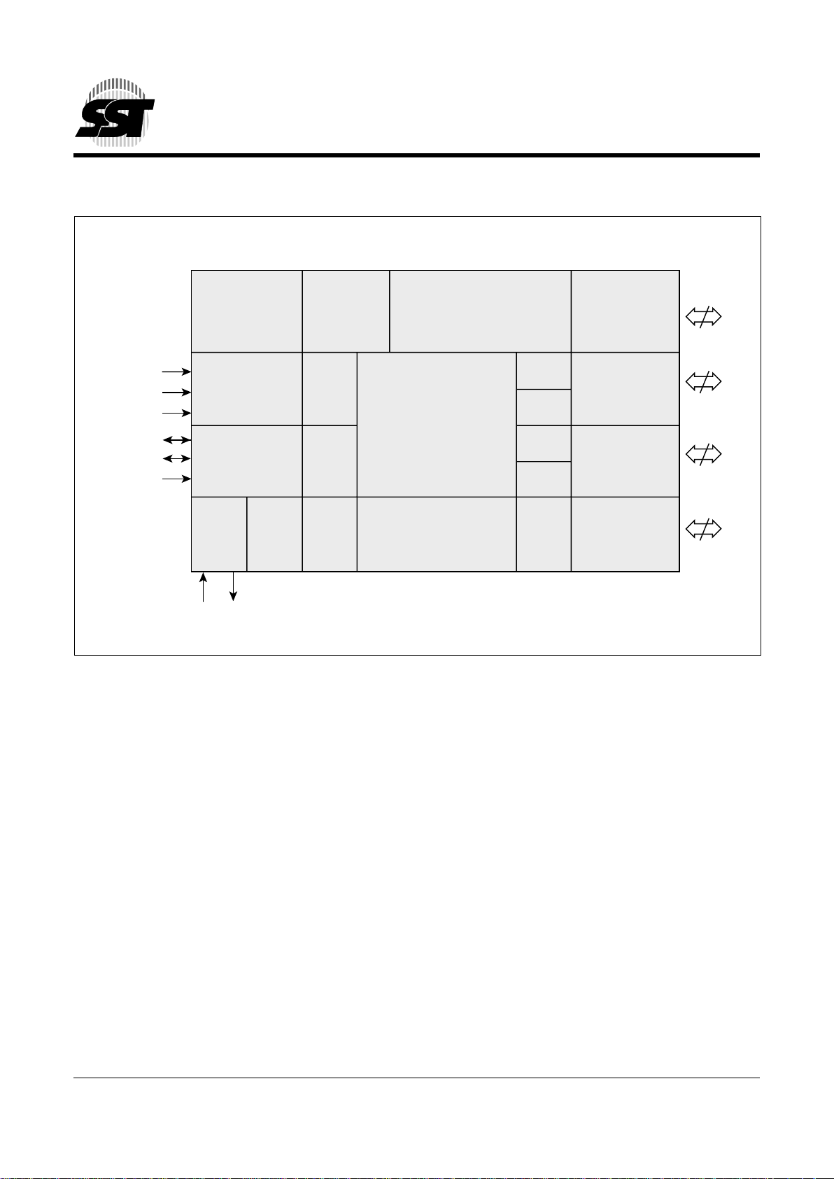
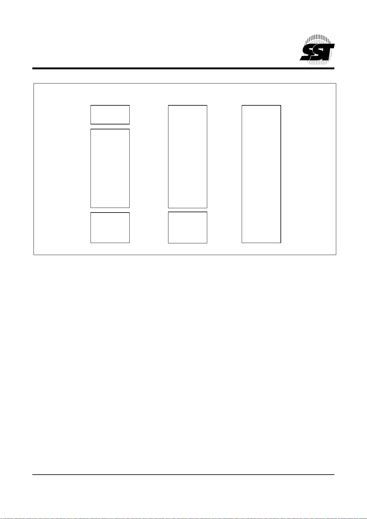
F
UNCTIONAL BLOCK DIAGRAM
FUNCTIONAL BLOCKS
RST
V
SS
V
DD
ALE/PROG#
PSEN#
EA#
XTAL1 XTAL2
SuperFlash
EEPROM
4K x 8
Program/Erase
& IAP
Control
SuperFlash EEPROM
16/32K x 8
CPU
Port 0
8
I/O
8
I/O
8
I/O
8
I/O
Port 1
Power Mode
Management
Bus Controller
T0
T1
T2
WDT
8-bit
UART
RAM
256 x 8
Interrupt
Control
SFRs
Security
Lock
Mode
Control
Oscillator
&
Timing
Port 2
Port 3
344 ILL B1.1
5
© 2000 Silicon Storage Technology, Inc. 344-2 8/00
FlashFlex51 MCU
SST89C54 / SST89C58
Preliminary Specifications
1
2
3
4
5
6
7
8
9
10
11
12
13
14
15
16
39
38
37
36
35
34
33
32
31
30
29
7
8
9
10
11
12
13
14
15
16
17
P1.5
P1.6
P1.7
RST
(RXD) P3.0
NC
(TXD) P3.1
(INT0#) P3.2
(INT1#) P3.3
(T0) P3.4
(T1) P3.5
P0.4 (AD4)
P0.5 (AD5)
P0.6 (AD6)
P0.7 (AD7)
EA#
NC
ALE/PROG#
PSEN#
P2.7 (A15)
P2.6 (A14)
P2.5 (A13)
6 5 4 3 2 1 44 43 42 41 40
18 19 20 21 22 23 24 25 26 27 28
P1.4
P1.3
P1.2
P1.1 (T2 Ex)
P1.0 (T2)NCVDDP0.0 (AD0)
P0.1 (AD1)
P0.2 (AD2)
P0.3 (AD3)
(WR#) P3.6
(RD#) P3.7
XTAL2
XTAL1
V
SS
NC
(A8) P2.0
(A9) P2.1
(A10) P2.2
(A11) P2.3
(A12) P2.4
44-Pin PLCC
T op Vie w
344 ILL F20.1
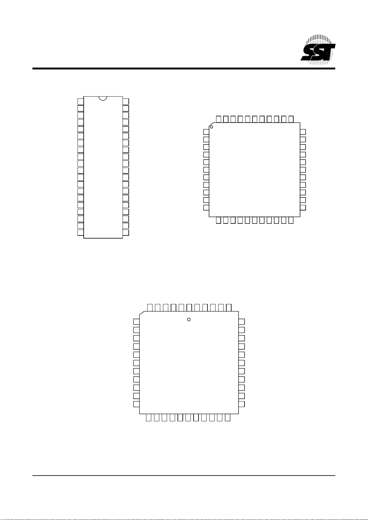
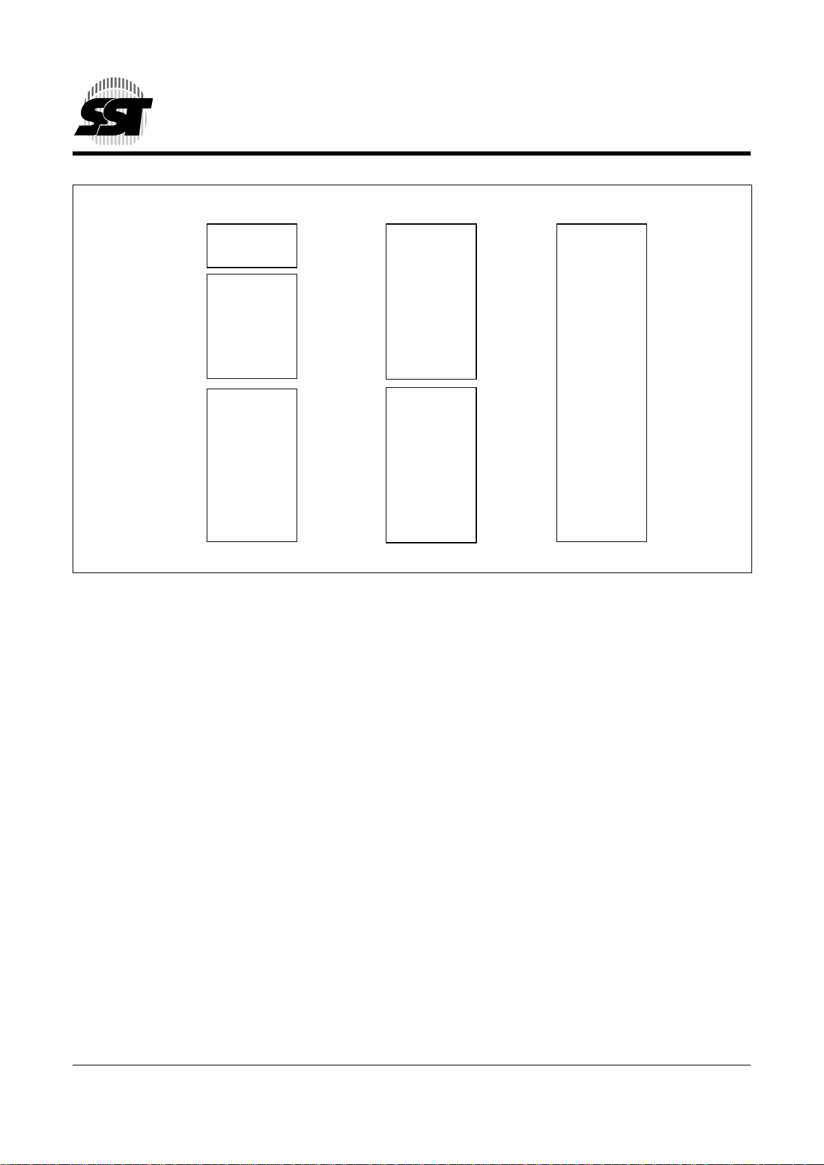
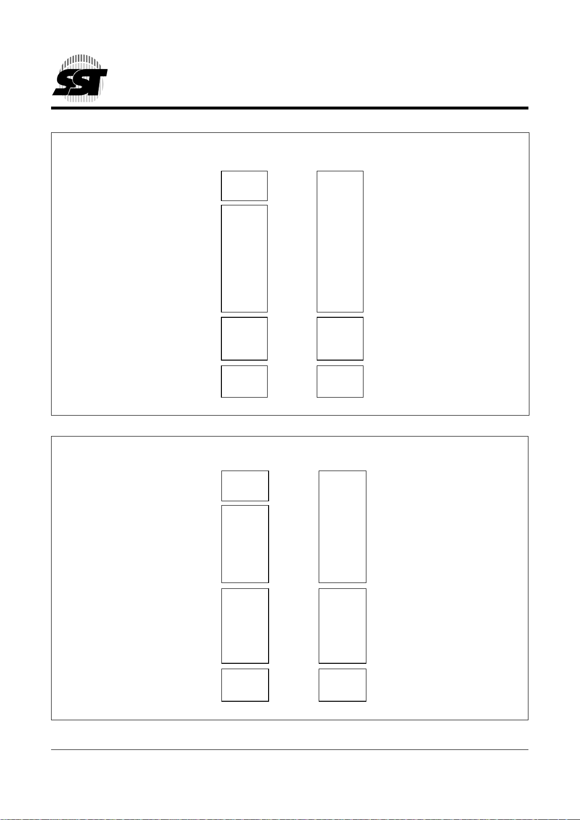
PIN ASSIGNMENTS
FIGURE 1: PIN ASSIGNMENTS FOR 40-PIN PLASTIC DIP
PI-PACKAGE
FIGURE 2: PIN ASSIGNMENTS FOR 44-PIN TQFP
TQJ-PACKAGE
Note: NC pins must be left unconnected.
FIGURE 3: PIN ASSIGNMENTS FOR 44-PIN PLCC
NJ-PACKAGE
40
39
38
37
36
35
34
33
32
31
30
29
28
27
26
25
24
23
22
21
(T2) P1.0
(T2 Ex) P1.1
P1.2
P1.3
P1.4
P1.5
P1.6
P1.7
RST
(RXD) P3.0
(TXD) P3.1
(INT0#) P3.2
(INT1#) P3.3
(T0) P3.4
(T1) P3.5
(WR#) P3.6
(RD#) P3.7
XTAL2
XTAL1
V
SS
1
2
3
4
5
6
7
8
9
10
11
12
13
14
15
16
17
18
19
20
V
DD
P0.0 (AD0)
P0.1 (AD1)
P0.2 (AD2)
P0.3 (AD3)
P0.4 (AD4)
P0.5 (AD5)
P0.6 (AD6)
P0.7 (AD7)
EA#
ALE/PROG#
PSEN#
P2.7 (A15)
P2.6 (A14)
P2.5 (A13)
P2.4 (A12)
P2.3 (A11)
P2.2 (A10)
P2.1 (A9)
P2.0 (A8)
40-Pin PDIP
T op View
344 ILL F18.1
33
32
31
30
29
28
27
26
25
24
23
12 13 14 15 16 17 18 19 20 21 22
1
2
3
4
5
6
7
8
9
10
11
P1.5
P1.6
P1.7
RST
(RXD) P3.0
NC
(TXD) P3.1
(INT0#) P3.2
(INT1#) P3.3
(T0) P3.4
(T1) P3.5
P0.4 (AD4)
P0.5 (AD5)
P0.6 (AD6)
P0.7 (AD7)
EA#
NC
ALE/PROG#
PSEN#
P2.7 (A15)
P2.6 (A14)
P2.5 (A13)
44 43 42 41 40 39 38 37 36 35 34
P1.4
P1.3
P1.2
P1.1 (T2 Ex)
P1.0 (T2)NCVDDP0.0 (AD0)
P0.1 (AD1)
P0.2 (AD2)
P0.3 (AD3)
(WR#) P3.6
(RD#) P3.7
XTAL2
XTAL1
V
SS
NC
(A8) P2.0
(A9) P2.1
(A10) P2.2
(A11) P2.3
(A12) P2.4
44-Pin TQFP
T op Vie w
344 ILL F19.1
6
© 2000 Silicon Storage Technology, Inc. 344-2 8/00
FlashFlex51 MCU
SST89C54 / SST89C58
Preliminary Specifications
TABLE 1: PIN DESCRIPTIONS
Symbol Type
1
Name and Functions
P0[7:0] I/O
1
Port 0: Port 0 is an 8-bit open drain bi-directional I/O port. As an output port each
pin can sink several LS TTL inputs. Port 0 pins that have 1’s written to them
float, and in that state can be used as high-impedance inputs. Port 0 is also the
multiplexed low-order address and data bus during accesses to external
memory. In this application it uses strong internal pull-ups when transitioning
to 1’s. Port 0 also receives the code bytes during FLASH MEMORY
programming, and outputs the code bytes during program verification. External
pull-ups are required during program verification.
P1[7:0] I/O with internal Port 1: Port 1 is an 8-bit bi-directional I/O port with internal pull-ups. The Port 1
pull-ups output buffers can drive LS TTL inputs. Port 1 pins that have 1’s written to them
are pulled high by the internal pull-ups, and in that state can be used as
inputs. As inputs, Port 1 pins that are externally pulled low will source current
(I
IL
, on the data sheet) because of the internal pull-ups. P1(5, 6, 7) have high
current drive of 16mA. Port 1 also receives the low-order address bytes during
FLASH MEMORY programming and program verification.
P1[0] I T2: (external count input to Timer/Counter 2), clock-out
P1[1] I T2EX: (Timer/Counter 2 capture/reload trigger and direction control)
P2[7:0] I/O with internal Port 2: Port 2 is an 8-bit bi-directional I/O port with internal pull-ups. Port 2 pins
pull-ups that have 1’s written to them are pulled high by the internal pull-ups, and
in that state can be used as inputs. As inputs, Port 2 pins that are externally
pulled low will source current (IIL, on the data sheet) because of the internal
pull-ups. Port 2 sends the high-order address byte during fetches from external
Program memory and during accesses to external Data Memory that use 16-bit
address (MOVX@DPTR). In this application it uses strong internal pull-ups
when outputting 1’s. During accesses to external Data Memory that use 8-bit
addresses (MOVX@Ri), Port 2 sends the contents of the P2 Special Function
Register. Port 2 also receives some control signals and a partial of high-order
address bits during FLASH MEMORY programming and program verification.
P3[7:0] I/O with internal Port 3: Port 3 is an 8-bit bidirectional I/O port with internal pull-ups. The Port 3
pull-ups output buffers could drive LS TTL inputs. Port 3 pins that have 1’s written to them
are pulled high by the internal pull-ups, and in that state can be used as inputs.
As inputs, Port 3 pins that are externally pulled low will source current (IIL, on the
data sheet) because of the pull-ups. Port 3 also serves the functions of various
special features of the FlashFlex51 Family. Port 3 also receives some control
signals and a partial of high-order address bits during FLASH MEMORY
programming and program verification.
P3[0] I RXD: Serial input line
P3[1] O TXD: Serial output line
P3[2] I INT0#: External Interrupt 0
P3[3] I INT1#: External Interrupt 1
P3[4] I T0: Timer 0 external input
P3[5] I T1: Timer 1 external input
P3[6] O WR#: External Data Memory Write strobe
P3[7] O RD#: External Data Memory Read strobe

7
© 2000 Silicon Storage Technology, Inc. 344-2 8/00
FlashFlex51 MCU
SST89C54 / SST89C58
Preliminary Specifications
1
2
3
4
5
6
7
8
9
10
11
12
13
14
15
16
PIN DESCRIPTIONS (CONTINUED)
Symbol Type
1
Name and Functions
PSEN# O/I Program Store Enable: PSEN# is the Read strobe to External Program
Memory. When the SST89C54/58 are executing from Internal Program
Memory, PSEN# is inactive (high). When the device is executing code from
External Program Memory, PSEN# is activated twice each machine cycle,
except that two PSEN# activations are skipped during each access to External
Data Memory. While the RST input is continually held high (for more than ten
machine cycles), a forced high-to-low input transition on the PSEN# pin will bring
the device into the “External Host” mode for the internal flash memory
programming operation.
RST I Reset: A high logic state on this pin for two machine cycles (at least 24 oscillator
periods), while the oscillator is running resets the device. After a successful reset
is completed, if the PSEN# pin is driven by an input force with a high-to-low
transition while the RST input pin is continually held high, the device will enter the
“External Host” mode for the internal flash memory programming operation,
otherwise the device will enter the “Normal” operation mode.
EA# I External Access Enable: EA# must be connected to VSS in order to enable the
SST89C54/58 to fetch code from External Program Memory locations starting
at 0000h up to FFFFh. Note, however, that if the Security Lock is activated on
either block, the logic level at EA# is internally latched during reset. EA# must be
connected to VDD for internal program execution. The EA# pin can tolerate a high
voltage2 of 12V (see Electrical Specification).
ALE/PROG# I/O Address Latch Enable: ALE is the output signal for latching the low byte of the
address during accesses to external memory. This pin is also the programming
pulse input (PROG#).
XTAL1 I Oscillator: Input and output to the inverting oscillator amplifier. XTAL1 is input to
XTAL2 O internal clock generation circuits from an external clock source.
V
DD
I Power Supply: Supply voltage during normal, Idle, Power Down, and Standby
Mode operations.
Vss I Ground: Circuit ground. (0V reference)
344 PGM T1.6
Note: 1) I = Input
O = Output
2) It is not necessary to receive a 12V programming supply voltage during flash programming.
8
© 2000 Silicon Storage Technology, Inc. 344-2 8/00
FlashFlex51 MCU
SST89C54 / SST89C58
Preliminary Specifications
MEMORY ORGANIZATION
The SST89C54/58 have separate address spaces for
program and data memory.
Program Memory
There are two internal flash memory blocks in the
SST89C54/58. The primary flash memory Block 0 has
16/32 KByte and occupies the address space 0000h to
3FFFh/7FFFh. The secondary flash memory Block 1 has
4 KByte and occupies the address space F000h to
FFFFh.
The 16/32K x8 primary SuperFlash block is organized as
128/256 uniform sectors with sector address from A15 to
A7. Each sector contains 2 rows with row address from
A15 to A6. Each row has 64 Bytes with byte address from
A5 to A0.
F
IGURE 4: SECTOR ORGANIZATION
The 4K x8 secondary SuperFlash block is organized as
64 uniform sectors with sector address from A15 to A6.
Each sector contains 2 rows with row address from A15
to A5. Each row contains 32 Bytes with byte address
from A4 to A0. Figure 4 shows the sector organization for
SST89C54/58.
When internal code operation is enabled (EA# = 1), the
primary 16/32 KByte flash memory block is always
visible to the program counter for code fetching. Figures
5 and 6 show the program memory organizations for the
SST89C54/58.
When internal code operation is enabled (EA# = 1), the
secondary 4 KByte flash memory block is selectively
visible for code fetching. The secondary block is always
accessible through the SuperFlash mailbox registers:
SFCM, SFCF, SFAL, SFAH, SFDT and SFST. When bit
7 of the SuperFlash Configuration mailbox register
(SFCF[7]), SFR address location B1h, is set, the secondary 4 KByte block will be visible by program counter.
7FFFh
7F80h
4000h
3FFFh
0000h
Block 0 (16/32 KByte)
344 ILL F47.6
Sector 255
Sector 127
Sector 0
3F80h
007Fh
FFFFh
FFC0h
F03Fh
Block 1 (4 KByte)
Primary Secondary
Sector 63
Sector 0
F000h
89C58
89C54
9
© 2000 Silicon Storage Technology, Inc. 344-2 8/00
FlashFlex51 MCU
SST89C54 / SST89C58
Preliminary Specifications
1
2
3
4
5
6
7
8
9
10
11
12
13
14
15
16
FIGURE 5: SST89C54 PROGRAM MEMORY ORGANIZATION
344 ILL F21.1
48 KByte
EXTERNAL
64 KByte
EXTERNAL
16 KByte
INTERNAL
(Block 0)
44 KByte
EXTERNAL
16 KByte
INTERNAL
(Block 0)
4 KByte
INTERNAL
(Block 1)
EA# = 1 & SFCF[7] = 1 EA# = 1 & SFCF[7] = 0 EA# = 0
FFFFh
EFFFh
F000h
4000h
0000h
3FFFh
FFFFh
4000h
0000h
FFFFh
0000h
3FFFh
10
© 2000 Silicon Storage Technology, Inc. 344-2 8/00
FlashFlex51 MCU
SST89C54 / SST89C58
Preliminary Specifications
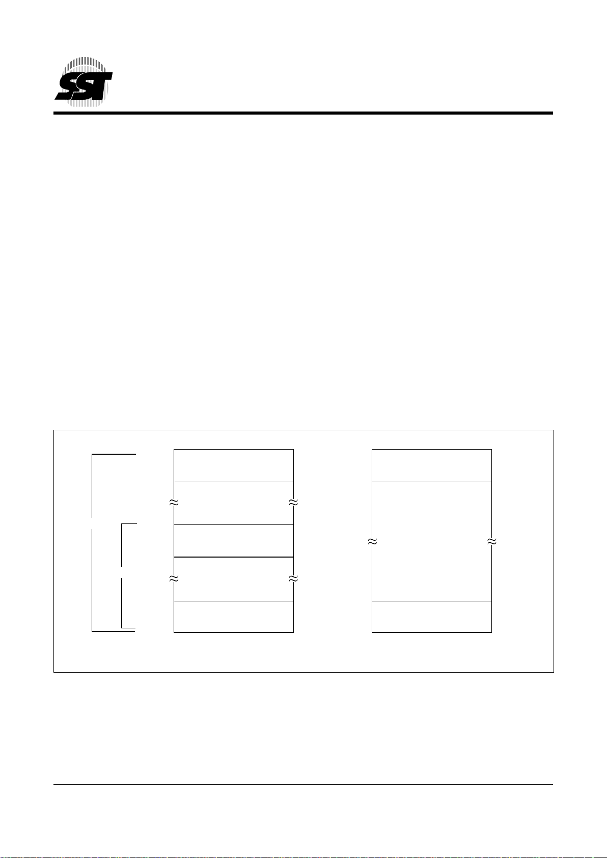
Memory Re-mapping
The SST89C54/58 memory re-mapping feature allows
users to reorganize internal Flash memory sectors so
that interrupts may be serviced when Block 0 of the
internal Flash is being programmed. Since Block 0
occupies the low order program address space of the
8051 architecture where the interrupt vectors reside,
those interrupt vectors will normally not be available
when Block 0 is being programmed.
SST89C54/58 provides four options of Memory Remapping (Refer to Table 2). When the lowest 4 KBytes
are remapped, any program access within logical address range 0000h – 0FFFh will have the 4 most significant address bits forced to “1”, redirecting the access to
F000h – FFFFh. Note that the physical contents of the
re-mapped portion of Block 0 (i.e. physical locations
0000h – 0FFFh in the current example) will not be
accessible. Block 1 will still also be accessible through
F000h – FFFFh. Figures 7 and 8 show re-mapped
program memory organization for the SST89C54/58.
FIGURE 6: SST89C58 PROGRAM MEMORY ORGANIZATION
344 ILL F11.1
32 KByte
EXTERNAL
64 KByte
EXTERNAL
32 KByte
INTERNAL
(Block 0)
28 KByte
EXTERNAL
32 KByte
INTERNAL
(Block 0)
4 KByte
INTERNAL
(Block 1)
EA# = 1 & SFCF[7] = 1 EA# = 1 & SFCF[7] = 0 EA# = 0
FFFFh
EFFFh
F000h
8000h
0000h
7FFFh
FFFFh
8000h
0000h
FFFFh
0000h
7FFFh

11
© 2000 Silicon Storage Technology, Inc. 344-2 8/00
FlashFlex51 MCU
SST89C54 / SST89C58
Preliminary Specifications
1
2
3
4
5
6
7
8
9
10
11
12
13
14
15
16
Activation and Deactivation of Memory Re-mapping
The actual amount of memory that is re-mapped is
controlled by MAP_EN[1:0] bits as shown in Table 2. The
MAP_EN[1:0] bits are the same bits as SFCF[1:0]. The
MAP_EN[1:0] bits are under software control and can be
changed during program execution. Since changing re-
mapping will cause program re-location, it is advisable
that the instruction that changes the MAP_EN[1:0] be in
the portion of memory that is not affected by the remapping change.
The MAP_EN[1:0] bits are initialized at Reset according
to the contents of two non-volatile register bits, ReMap[1:0] (as shown in Table 2). The Re-Map[1:0] bits are
programmed via PROG_RB1 and PROG_RB0 External
Host Mode commands. Refer to External Host Program-
ming Mode section for PROG_RB1 and PROG_RB0
commands.
The contents of MAP_EN[1:0] are only updated according to Re-Map[1:0] on a successful reset. Any subsequent alteration to the Re-Map[1:0] bits will not automatically change the MAP_EN[1:0] bits without a reset.
Similarly, changes to MAP_EN[1:0] during program execution will not change Re-Map[1:0] bits.
To deactivate memory re-mapping, a CHIP-ERASE operation will revert Re-Map[1:0] to the default status of
“11”, disabling re-mapping. Programming 00b to
SFCF[1:0] register also deactivates memory re-mapping. The effect of programming Re-Map[1:0] is available
only after the next reset. Refer to In-Application Mode
Commands section for more detailed information.
TABLE 2: RE-MAPPING TABLE
Re-Map [1:0]
1
MAP_EN
2,3
Comments
11 00 Re-mapping is turned off. Program memory is in normal
configuration.
10 01 1 KByte of flash memory location is re-mapped. Program access
to location 0000h-03FFh is redirected to F000h – F3FFh.
01 10 2 KBytes of flash memory location are re-mapped. Program access
to location 0000h-07FFh is redirected to F000h – F7FFh.
00 11 4 KBytes of flash memory location is re-mapped. Program access
to location 0000h-0FFFh is redirected to F000h – FFFFh.
1 Re-Map[1:0] are nonvolatile registers which are examined only during Reset.
2 MAP_EN[1:0] are initialized according to Re-Map[1:0] during Reset.
3 MAP_EN[1:0] are located in SFCF[1:0], they determine the Re-Mapping configuration. They may be changed by the program at run time.
344 PGM T2.3
12
© 2000 Silicon Storage Technology, Inc. 344-2 8/00
FlashFlex51 MCU
SST89C54 / SST89C58
Preliminary Specifications
F
IGURE 7: SST89C54 RE-MAPPED PROGRAM MEMORY ORGANIZATION
FIGURE 8: SST89C58 RE-MAPPED PROGRAM MEMORY ORGANIZATION
28 KByte
EXTERNAL
31/30/28
KByte
INTERNAL
(Block 0)
1/2/4 KByte
INTERNAL
(Block 1)
4 KByte
INTERNAL
(Block 1)
EA# = 1 & SFCF[7] = 1
SFCF [1:0] = 01/10/11
FFFFh
EFFFh
F000h
7FFFh
8000h
7FFFh
8000h
0000h
32 KByte
EXTERNAL
31/30/28
KByte
INTERNAL
(Block 0)
1/2/4 KByte
INTERNAL
(Block 1)
344 ILL F36.1
EA# = 1 & SFCF[7] = 0
SFCF [1:0] = 01/10/11
FFFFh
0000h
44 KByte
EXTERNAL
15/14/12
KByte
INTERNAL
(Block 0)
1/2/4 KByte
INTERNAL
(Block 1)
4 KByte
INTERNAL
(Block 1)
EA# = 1 & SFCF[7] = 1
SFCF [1:0] = 01/10/11
FFFFh
EFFFh
F000h
3FFFh
4000h
3FFFh
4000h
0000h
48 KByte
EXTERNAL
15/14/12
KByte
INTERNAL
(Block 0)
1/2/4 KByte
INTERNAL
(Block 1)
344 ILL F35.3
EA# = 1 & SFCF[7] = 0
SFCF [1:0] = 01/10/11
FFFFh
0000h
13
© 2000 Silicon Storage Technology, Inc. 344-2 8/00
FlashFlex51 MCU
SST89C54 / SST89C58
Preliminary Specifications
1
2
3
4
5
6
7
8
9
10
11
12
13
14
15
16
Data Memory
SST89C54/58 have 256 x 8 bits of on-chip RAM and can address up to 64 KBytes of external data memory.
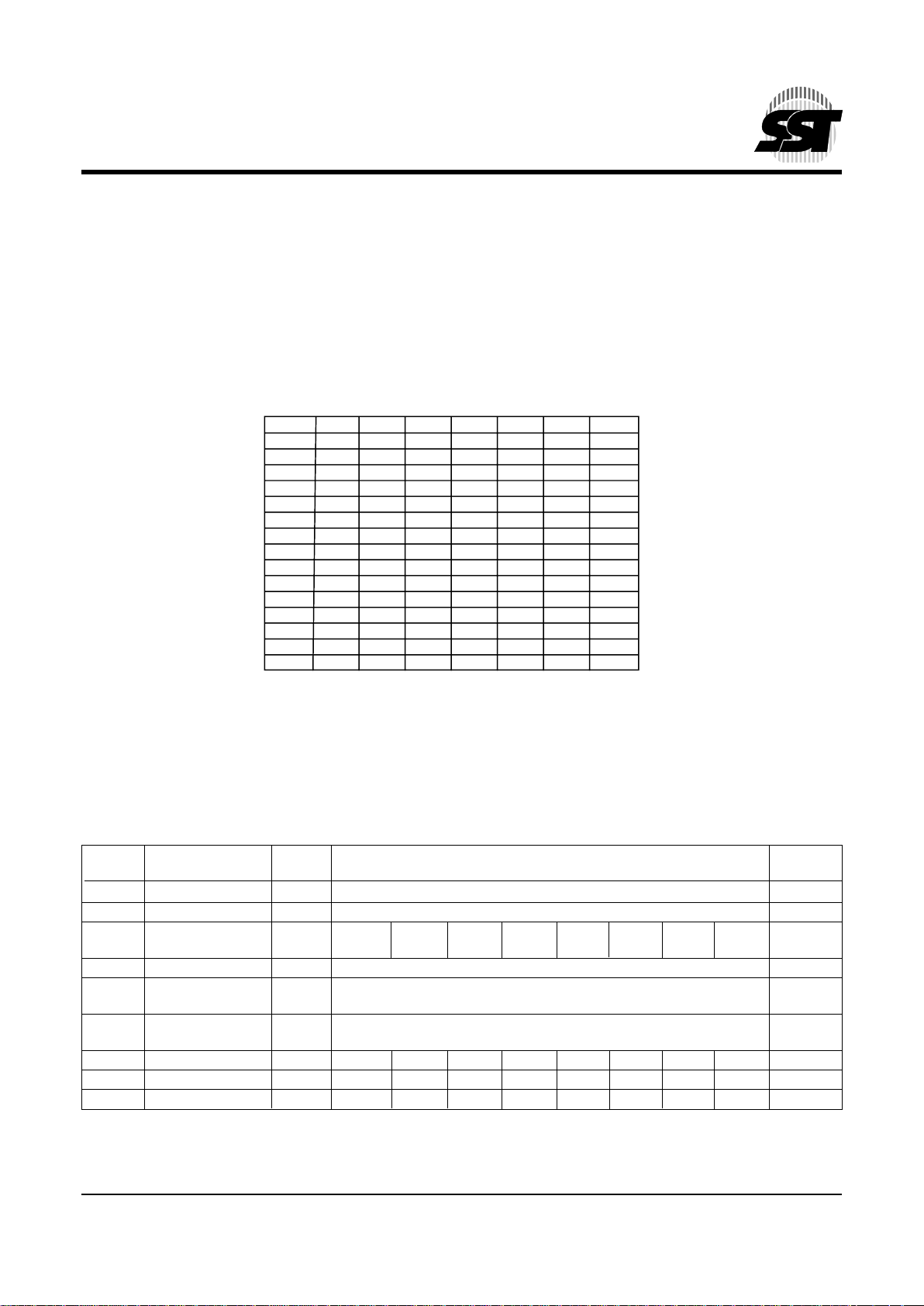
Special Function Registers (SFR)
Most of the unique features of the FlashFlex51 microcontroller family are controlled by bits in special function registers
(SFRs) located in the FlashFlex51 SFR Memory Map shown below. Individual descriptions of each SFR are provided
and Reset values indicated in Tables 3
A to 3E.
F8
F0
E8
E0
D8
D0
C8
C0
B8
B0
A8
A0
98
90
88
80
FF
F7
EF
E7
DF
D7
CF
C7
BF
B7
AF
A7
9F
97
8F
87
B*
ACC*
PSW*
T2CON*
RCAP2L
RCAP2H
TL2 TH2
WDTC*
IP*
P3* SFCF SFCM SFAL SFAH SFDT SFST
IE*
P2*
SCON*
SBUF
P1*
TCON* TMOD TL0 TL1 TH0 TH1
P0* SP DPL DPH WDTD PCON
8 BYTES
FlashFlex51 SFR Memory Map
* = Bit Addressable SFRs
All addresses are hexadecimal
344 ILL F23.1
SST89C54/58 Special Function Registers
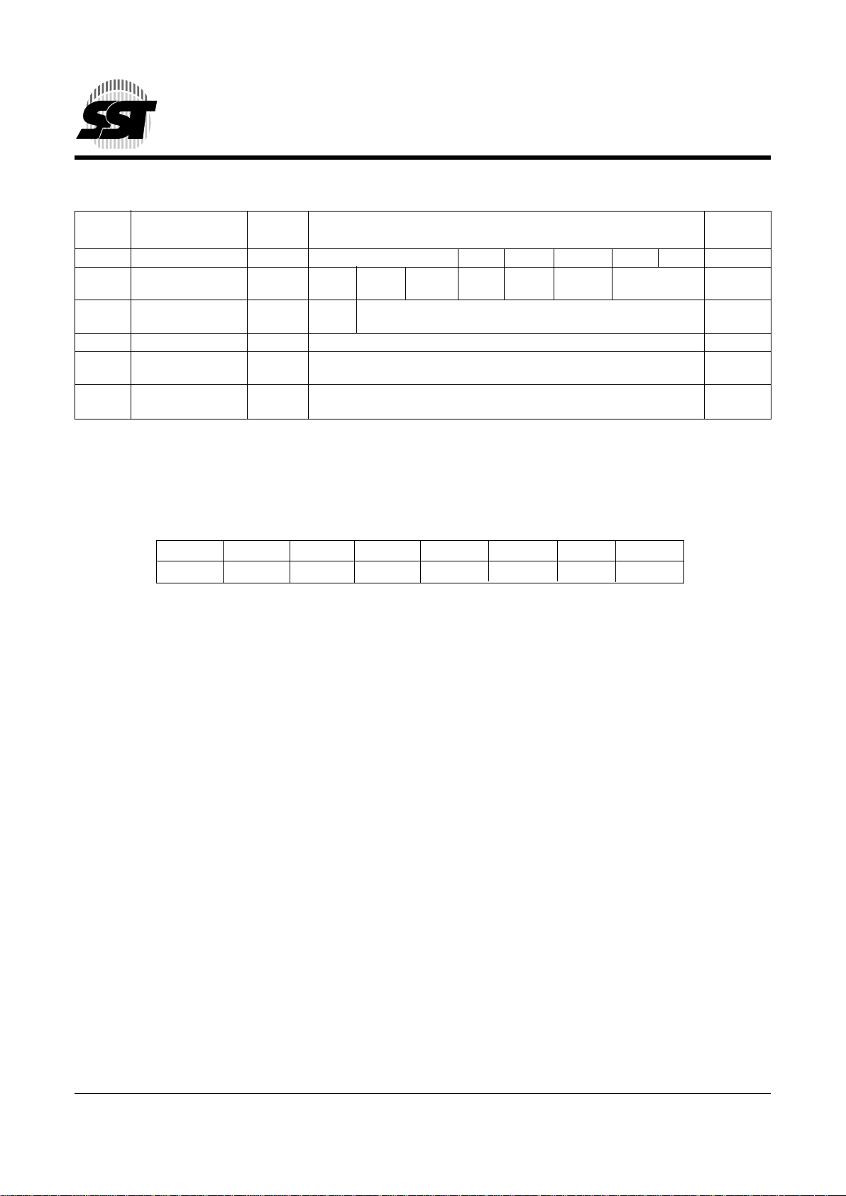
TABLE 3A: CPU RELATED SFRS
Symbol Description Direct Bit Address, Symbol, or Alternative Port Function RESET
Address MSB LSBValue
ACC* Accumulator E0h ACC[7:0] 00h
B* B Register F0h B[7:0] 00h
PSW* Program Status D0h CY AC F0 RS1 RS0 OV F1 P 0 0h
Word
SP Stack Pointer 81h SP[7:0] 07h
DPL Data Pointer 82h DPL[7:0] 00h
Low 0
DPH Data Pointer 83h DPH[7:0] 00h
High 0
IE* Interrupt Enable A8h EA - ET2 ES0 ET1 EX1 ET0 EX0 40h
IP* Interrupt Priority B8h - - PT2 PS PT1 PX1 PT0 PX0 xx000000b
PCON Power Control 87h SMOD - - - GF1 GF0 PD IDL 0xxx0000b
* = Bit Addressable SFRs
344 PGM T3A.3
14
© 2000 Silicon Storage Technology, Inc. 344-2 8/00
FlashFlex51 MCU
SST89C54 / SST89C58
Preliminary Specifications
SuperFlash Status Register (SFST) (Read Only Register)
Location 76543210Reset Value
0B6h SECD2 SECD1 SECD0 – Busy Flash_busy ––xxx00000b
Symbol Function
SECD2 Security bit 1.
SECD1 Security bit 2.
SECD0 Security bit 3.
Please refer to Table 8 for security lock options.
BUSY Burst-Program completion polling bit.
1: Device is busy with flash operation.
0: Device is available for next Burst-Program operation.
Flash_busy Flash operation completion polling bit.
1: Device is busy with flash operation.
0: Device has fully completed the last command, including Burst-Program.
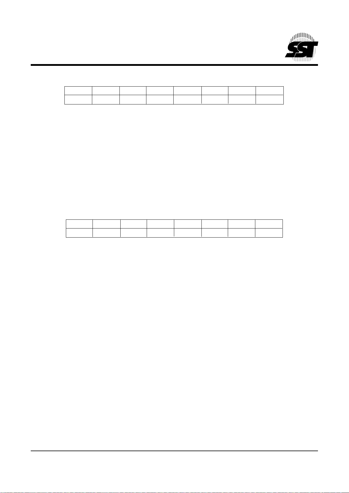
TABLE 3B: FLASH MEMORY PROGRAMMING SFRS
Symbol Description Direct Bit Address, Symbol, or Alternative Port Function RESET
Address MSB LSB Value
SFST SuperFlash Status B6h SECD[2:0] - BUSY
Flash_busy
- - xxx00000b
SFCF SuperFlash B1h VIS IAPEN - - - - MAP_EN 000000xxb
Configuration
SFCM SuperFlash B2h FIE FCM 00h
Command
SFDT SuperFlash Data B5h SuperFlash Data Register 00h
SFAL SuperFlash B3h SuperFlash Low Order Byte Address Register – A7 to A0 (SFAL) 00h
Address Low
SFAH SuperFlash B4h SuperFlash High Order Byte Address Register – A15 to A8 (SFAH) 00h
Address High
344 PGM T3B.4
15
© 2000 Silicon Storage Technology, Inc. 344-2 8/00
FlashFlex51 MCU
SST89C54 / SST89C58
Preliminary Specifications
1
2
3
4
5
6
7
8
9
10
11
12
13
14
15
16
SuperFlash Configuration Register (SFCF)
Location 76543210Reset Value
0B1h VIS IAPEN ––––
MAP_EN1 MAP_EN0
000000xxb
Symbol Function
VIS Upper flash block visibility.
1: 4 KByte flash block visible from F000-FFFF.
0: 4 KByte flash block not visible.
IAPEN Enable IAP operation.
1: IAP commands are enabled.
0: IAP commands are disabled.
MAP_EN1 Map enable bit 1.
MAP_EN0 Map enable bit 0.
MAP_EN[1:0] are initialized to default value according to Re-map [1:0] during Reset.
Refer to Table 2.
SuperFlash Command Register (SFCM)
Location 76543210Reset Value
0B2h FIE FCM6 FCM5 FCM4 FCM3 FCM2 FCM1 FCM0 00000000b
Symbol Function
FIE Flash Interrupt Enable.
1: INT1# is re-assigned to signal IAP operation completion.
External INT1# interrupts are ignored.
0: INT1# is not reassigned.
FCM[6:0] Flash operation command.
000_0001b Chip-Erase.
000_0110b Burst-Program.
000_1011b Sector-Erase.
000_1100b Byte-Verify.
(1)
000_1101b Block-Erase.
000_1110b Byte-Program.
All other combinations are not implemented, and reserved for future use.
(1)
Byte-Verify has a single machine cycle latency and will not generate any INT1# interrupt regardless of FIE.
 Loading...