

Silicon Storage Technology Inc SST65P542R-8-C-SG Datasheet

Remote Controller MCU
SST65P542R
SST65P542RMicrocontroller
FEATURES:
• 8-bit MCU Core
– Enhanced 6502 Microprocessor Megacell emulating
the reduced 6805 instruction set
• 4 MHz Typical Oscillator Clock Frequency
• 8 MHz Maximum Oscillator Clock Frequency
• Low Voltage Operation: 2.2-3.2V
• 20 Re-configurable General Purpose I/O leads
• SuperFlash Memory
– 16 KByte of Flash Memory
– 128 Byte sectors for SoftPartition
– 100,000 endurance cycles (typical)
– 100 years data retention
– Fast Write:
- Chip-Erase: 70 ms (typical)
- Sector-Erase: 18 ms (typical)
- Byte-Program: 60 µs (typical)
– In-Application Programming (IAP)
Advance Information
• External Host Programming Mode for
Programmer Support
– JEDEC Standard Command Sets
• 352 Byte On-Chip SRAM
• In-System Programming (ISP) Support
through Firmware
• IR Input Pin for Learning Mode
• Carrier Modulator Transmitter
– Supports Baseband, Pulse Length Modulator
(PLM), and Frequency Shift Keying (FSK)
• Core Timer / Counter
– 14-stage multifunctional ripple counter
– Includes timer overflow, POR, RTI, and CWT
• External Reset Input and Low Power Pins
•Power Management
– Hardware enable bits programmable by software
for entering STOP and IDLE modes
• Package Available
– 28-lead SOIC
PRODUCT DESCRIPTION
The SST65P542R is a member of SST’s 8-bit application
specific microcontroller family targeted for IR remote controller applications.
The SST65P542R microcontroller provides high functionality to infrared remote controller products. The device offers
flexibility to store different remote control configurations for
controlling multiple appliances. The configurations are
either programmed at the factory during the manufacturing
process or downloaded through firmware.
Using SST’s SuperFlash nonvolatile memory technology,
the SST65P542R enhances the functionality and reduces
the cost of conventional universal remote controller devices
by integrating multiple functions of a remote controller system in a single chip solution. The built-in LED I/O ports can
directly drive LED indicators. The IR transmitter port drives
signals to the infrared transmitter, which, in turn, remotely
controls the appliances.
The SoftPartition architecture allows seamless flash memory partitioning of the program code, protocol tables, and
user data in the small granularity of 128 Byte sectors. The
small sector size and fast Write capability of the device
greatly decreases the time and power when altering the
contents of the flash memory.
The highly reliable, patented SuperFlash technology
provides significant advantage over conventional flash
memory technology. These advantages translate into
significant cost saving and reliability benefits for the
customers.
©2001 Silicon Stor age Technology, Inc.
S71170-03-000 12/01 368
1
SST, the SST logo, and SuperFlash are Trademarks registered by Silicon Storage Technology, Inc. in the U.S. Patent and Trademark Office.
In-Application Programming, IAP, and SoftPartition are trademarks of Silicon Storage Technology, Inc.
These specifications are subject to change without notice.

Remote Controller MCU
SST65P542R
Advance Information
TABLE OF CONTENTS
PRODUCT DESCRIPTION . . . . . . . . . . . . . . . . . . . . . . . . . . . . . . . . . . . . . . . . . . . . . . . . . . . . . . . . . . . . . . . . . . . 1
LIST OF FIGURES . . . . . . . . . . . . . . . . . . . . . . . . . . . . . . . . . . . . . . . . . . . . . . . . . . . . . . . . . . . . . . . . . . . . . . . . . 4
LIST OF TABLES. . . . . . . . . . . . . . . . . . . . . . . . . . . . . . . . . . . . . . . . . . . . . . . . . . . . . . . . . . . . . . . . . . . . . . . . . . . 4
1.0 FUNCTIONAL BLOCKS . . . . . . . . . . . . . . . . . . . . . . . . . . . . . . . . . . . . . . . . . . . . . . . . . . . . . . . . . . . . . . . . . 5
Functional Block Diagram . . . . . . . . . . . . . . . . . . . . . . . . . . . . . . . . . . . . . . . . . . . . . . . . . . . . . . . . . . . . . . . . 5
2.0 PIN ASSIGNMENTS . . . . . . . . . . . . . . . . . . . . . . . . . . . . . . . . . . . . . . . . . . . . . . . . . . . . . . . . . . . . . . . . . . . . 6
2.1 Pin Descriptions . . . . . . . . . . . . . . . . . . . . . . . . . . . . . . . . . . . . . . . . . . . . . . . . . . . . . . . . . . . . . . . . . . . . 6
3.0 I/O REGISTERS AND MEMORY ORGANIZATION . . . . . . . . . . . . . . . . . . . . . . . . . . . . . . . . . . . . . . . . . . . . 7
3.1 I/O Registers . . . . . . . . . . . . . . . . . . . . . . . . . . . . . . . . . . . . . . . . . . . . . . . . . . . . . . . . . . . . . . . . . . . . . . 8
3.2 SRAM. . . . . . . . . . . . . . . . . . . . . . . . . . . . . . . . . . . . . . . . . . . . . . . . . . . . . . . . . . . . . . . . . . . . . . . . . . . 19
3.3 SuperFlash Memory. . . . . . . . . . . . . . . . . . . . . . . . . . . . . . . . . . . . . . . . . . . . . . . . . . . . . . . . . . . . . . . . 19
4.0 PARALLEL INPUT/OUTPUT PORTS. . . . . . . . . . . . . . . . . . . . . . . . . . . . . . . . . . . . . . . . . . . . . . . . . . . . . . 20
4.1 Port A . . . . . . . . . . . . . . . . . . . . . . . . . . . . . . . . . . . . . . . . . . . . . . . . . . . . . . . . . . . . . . . . . . . . . . . . . . . 20
4.2 Port B . . . . . . . . . . . . . . . . . . . . . . . . . . . . . . . . . . . . . . . . . . . . . . . . . . . . . . . . . . . . . . . . . . . . . . . . . . . 20
4.3 Port C. . . . . . . . . . . . . . . . . . . . . . . . . . . . . . . . . . . . . . . . . . . . . . . . . . . . . . . . . . . . . . . . . . . . . . . . . . . 20
5.0 FLASH MEMORY PROGRAMMING . . . . . . . . . . . . . . . . . . . . . . . . . . . . . . . . . . . . . . . . . . . . . . . . . . . . . . 21
5.1 In-Application Programming. . . . . . . . . . . . . . . . . . . . . . . . . . . . . . . . . . . . . . . . . . . . . . . . . . . . . . . . . . 21
5.1.1 Chip-Erase . . . . . . . . . . . . . . . . . . . . . . . . . . . . . . . . . . . . . . . . . . . . . . . . . . . . . . . . . . . . . . . . . . 21
5.1.2 Sector-Erase . . . . . . . . . . . . . . . . . . . . . . . . . . . . . . . . . . . . . . . . . . . . . . . . . . . . . . . . . . . . . . . . 21
5.1.3 Byte-Program . . . . . . . . . . . . . . . . . . . . . . . . . . . . . . . . . . . . . . . . . . . . . . . . . . . . . . . . . . . . . . . . 21
5.2 External Host Programming Mode . . . . . . . . . . . . . . . . . . . . . . . . . . . . . . . . . . . . . . . . . . . . . . . . . . . . . 21
5.2.1 External Host Mode Read Operation . . . . . . . . . . . . . . . . . . . . . . . . . . . . . . . . . . . . . . . . . . . . . . 21
5.2.2 External Host Mode Write Operation . . . . . . . . . . . . . . . . . . . . . . . . . . . . . . . . . . . . . . . . . . . . . . 22
5.2.3 External Host Mode Byte-Program Operation . . . . . . . . . . . . . . . . . . . . . . . . . . . . . . . . . . . . . . . 22
5.2.4 External Host Mode Chip-Erase Operation. . . . . . . . . . . . . . . . . . . . . . . . . . . . . . . . . . . . . . . . . . 22
5.2.5 External Host Mode Sector-Erase Operation . . . . . . . . . . . . . . . . . . . . . . . . . . . . . . . . . . . . . . . . 22
5.2.6 Operation Status Detection - Program Timer Method . . . . . . . . . . . . . . . . . . . . . . . . . . . . . . . . . 23
5.2.7 Operation Status Detection - RY/BY# Method . . . . . . . . . . . . . . . . . . . . . . . . . . . . . . . . . . . . . . . 23
5.2.8 Exiting The External Host Programming Mode . . . . . . . . . . . . . . . . . . . . . . . . . . . . . . . . . . . . . . 23
5.2.9 Flash Read Protection . . . . . . . . . . . . . . . . . . . . . . . . . . . . . . . . . . . . . . . . . . . . . . . . . . . . . . . . . 23
6.0 RESET . . . . . . . . . . . . . . . . . . . . . . . . . . . . . . . . . . . . . . . . . . . . . . . . . . . . . . . . . . . . . . . . . . . . . . . . . . . . . 24
6.1 External Reset . . . . . . . . . . . . . . . . . . . . . . . . . . . . . . . . . . . . . . . . . . . . . . . . . . . . . . . . . . . . . . . . . . . . 24
6.2 External Low Power Reset. . . . . . . . . . . . . . . . . . . . . . . . . . . . . . . . . . . . . . . . . . . . . . . . . . . . . . . . . . . 24
6.3 Internal Power-on and Brown-out Reset . . . . . . . . . . . . . . . . . . . . . . . . . . . . . . . . . . . . . . . . . . . . . . . . 24
6.4 COP Watchdog Timer Reset . . . . . . . . . . . . . . . . . . . . . . . . . . . . . . . . . . . . . . . . . . . . . . . . . . . . . . . . . 24
6.5 Illegal Address Reset . . . . . . . . . . . . . . . . . . . . . . . . . . . . . . . . . . . . . . . . . . . . . . . . . . . . . . . . . . . . . . . 24
©2001 Silicon Storage Technology, Inc. S71170-03-000 12/01 368
2

Remote Controller MCU
SST65P542R
Advance Information
7.0 INTERRUPTS . . . . . . . . . . . . . . . . . . . . . . . . . . . . . . . . . . . . . . . . . . . . . . . . . . . . . . . . . . . . . . . . . . . . . . . . 25
7.1 Software Interrupt. . . . . . . . . . . . . . . . . . . . . . . . . . . . . . . . . . . . . . . . . . . . . . . . . . . . . . . . . . . . . . . . . . 25
7.2 External Interrupts . . . . . . . . . . . . . . . . . . . . . . . . . . . . . . . . . . . . . . . . . . . . . . . . . . . . . . . . . . . . . . . . . 25
7.3 CMT Interrupt. . . . . . . . . . . . . . . . . . . . . . . . . . . . . . . . . . . . . . . . . . . . . . . . . . . . . . . . . . . . . . . . . . . . . 25
7.4 Core Timer Interrupt. . . . . . . . . . . . . . . . . . . . . . . . . . . . . . . . . . . . . . . . . . . . . . . . . . . . . . . . . . . . . . . . 25
8.0 OPERATION MODES. . . . . . . . . . . . . . . . . . . . . . . . . . . . . . . . . . . . . . . . . . . . . . . . . . . . . . . . . . . . . . . . . . 26
8.1 User Mode . . . . . . . . . . . . . . . . . . . . . . . . . . . . . . . . . . . . . . . . . . . . . . . . . . . . . . . . . . . . . . . . . . . . . . . 26
8.2 Learning Mode . . . . . . . . . . . . . . . . . . . . . . . . . . . . . . . . . . . . . . . . . . . . . . . . . . . . . . . . . . . . . . . . . . . . 26
9.0 PERIPHERALS AND OTHERS . . . . . . . . . . . . . . . . . . . . . . . . . . . . . . . . . . . . . . . . . . . . . . . . . . . . . . . . . . 27
9.1 Core Timer . . . . . . . . . . . . . . . . . . . . . . . . . . . . . . . . . . . . . . . . . . . . . . . . . . . . . . . . . . . . . . . . . . . . . . . 27
9.2 Carrier Modulator Transmitter (CMT). . . . . . . . . . . . . . . . . . . . . . . . . . . . . . . . . . . . . . . . . . . . . . . . . . . 27
9.3 Clock Input Options . . . . . . . . . . . . . . . . . . . . . . . . . . . . . . . . . . . . . . . . . . . . . . . . . . . . . . . . . . . . . . . . 27
9.4 Crystal/Ceramic Resonator . . . . . . . . . . . . . . . . . . . . . . . . . . . . . . . . . . . . . . . . . . . . . . . . . . . . . . . . . . 27
9.5 External Clock Drive. . . . . . . . . . . . . . . . . . . . . . . . . . . . . . . . . . . . . . . . . . . . . . . . . . . . . . . . . . . . . . . . 27
10.0 POWER SAVING MODES . . . . . . . . . . . . . . . . . . . . . . . . . . . . . . . . . . . . . . . . . . . . . . . . . . . . . . . . . . . . . . 28
10.1 STOP Mode . . . . . . . . . . . . . . . . . . . . . . . . . . . . . . . . . . . . . . . . . . . . . . . . . . . . . . . . . . . . . . . . . . . . . 28
10.2 IDLE Mode . . . . . . . . . . . . . . . . . . . . . . . . . . . . . . . . . . . . . . . . . . . . . . . . . . . . . . . . . . . . . . . . . . . . . . 28
11.0 ELECTRICAL SPECIFICATION . . . . . . . . . . . . . . . . . . . . . . . . . . . . . . . . . . . . . . . . . . . . . . . . . . . . . . . . . . 29
11.1 Absolute Maximum Stress Ratings . . . . . . . . . . . . . . . . . . . . . . . . . . . . . . . . . . . . . . . . . . . . . . . . . . . 29
11.2 Reliability Characteristics . . . . . . . . . . . . . . . . . . . . . . . . . . . . . . . . . . . . . . . . . . . . . . . . . . . . . . . . . . . 29
11.3 DC Specifications. . . . . . . . . . . . . . . . . . . . . . . . . . . . . . . . . . . . . . . . . . . . . . . . . . . . . . . . . . . . . . . . . 29
11.4 DC Electrical Characteristics . . . . . . . . . . . . . . . . . . . . . . . . . . . . . . . . . . . . . . . . . . . . . . . . . . . . . . . . 30
11.5 AC Electrical Characteristics . . . . . . . . . . . . . . . . . . . . . . . . . . . . . . . . . . . . . . . . . . . . . . . . . . . . . . . . 31
12.0 PRODUCT ORDERING INFORMATION . . . . . . . . . . . . . . . . . . . . . . . . . . . . . . . . . . . . . . . . . . . . . . . . . . . 39
12.1 Valid Combinations . . . . . . . . . . . . . . . . . . . . . . . . . . . . . . . . . . . . . . . . . . . . . . . . . . . . . . . . . . . . . . . 39
13.0 PACKAGING DIAGRAMS . . . . . . . . . . . . . . . . . . . . . . . . . . . . . . . . . . . . . . . . . . . . . . . . . . . . . . . . . . . . . . 40
©2001 Silicon Storage Technology, Inc. S71170-03-000 12/01 368
3

Remote Controller MCU
SST65P542R
Advance Information
LIST OF FIGURES
FIGURE 2-1: Pin Assignments for 28-lead SOIC . . . . . . . . . . . . . . . . . . . . . . . . . . . . . . . . . . . . . . . . . . . . . . 6
FIGURE 3-1: Memory Map. . . . . . . . . . . . . . . . . . . . . . . . . . . . . . . . . . . . . . . . . . . . . . . . . . . . . . . . . . . . . . . 7
FIGURE 4-1: Port B Interrupt and Pull-Up Options . . . . . . . . . . . . . . . . . . . . . . . . . . . . . . . . . . . . . . . . . . . 20
FIGURE 6-1: Reset Block Diagram . . . . . . . . . . . . . . . . . . . . . . . . . . . . . . . . . . . . . . . . . . . . . . . . . . . . . . . 24
FIGURE 9-1: Using the Crystal . . . . . . . . . . . . . . . . . . . . . . . . . . . . . . . . . . . . . . . . . . . . . . . . . . . . . . . . . . 27
FIGURE 9-2: External Clock Drive . . . . . . . . . . . . . . . . . . . . . . . . . . . . . . . . . . . . . . . . . . . . . . . . . . . . . . . . 27
FIGURE 10-1: Stop Mode and Idle Mode. . . . . . . . . . . . . . . . . . . . . . . . . . . . . . . . . . . . . . . . . . . . . . . . . . . 28
FIGURE 11-1: External Host Programming Mode - Setup Cycle Timing Diagram. . . . . . . . . . . . . . . . . . . . 32
FIGURE 11-2: External Host Programming Mode - Read Cycle Timing Diagram . . . . . . . . . . . . . . . . . . . . 32
FIGURE 11-3: External Host Programming Mode - Write Cycle Timing Diagram . . . . . . . . . . . . . . . . . . . . 33
FIGURE 11-4: External Host Programming Mode - Chip-Erase Timing Diagram . . . . . . . . . . . . . . . . . . . . 33
FIGURE 11-5: External Host Programming Mode Sector-Erase Timing Diagram . . . . . . . . . . . . . . . . . . . . 34
FIGURE 11-6: External Host Programming Mode Byte-Program Timing Diagram . . . . . . . . . . . . . . . . . . . 34
FIGURE 11-7: AC Input/Output Reference Waveform . . . . . . . . . . . . . . . . . . . . . . . . . . . . . . . . . . . . . . . . . 35
FIGURE 11-8: A Test Load Example . . . . . . . . . . . . . . . . . . . . . . . . . . . . . . . . . . . . . . . . . . . . . . . . . . . . . . 35
FIGURE 11-9: Byte-Program Command Sequence for External Host Programming Mode . . . . . . . . . . . . 36
FIGURE 11-10: Wait Options for External Host Programming Mode. . . . . . . . . . . . . . . . . . . . . . . . . . . . . . 37
FIGURE 11-11: Chip-/Sector-Erase Command Sequence for External Host Programming Mode . . . . . . . 38
LIST OF TABLES
TABLE 2-1: Pin Descriptions . . . . . . . . . . . . . . . . . . . . . . . . . . . . . . . . . . . . . . . . . . . . . . . . . . . . . . . . . . . . 6
TABLE 3-1: Register Descriptions and Bit Definitions . . . . . . . . . . . . . . . . . . . . . . . . . . . . . . . . . . . . . . . . . 8
TABLE 3-5: Interrupt/Reset Sector. . . . . . . . . . . . . . . . . . . . . . . . . . . . . . . . . . . . . . . . . . . . . . . . . . . . . . . 19
TABLE 5-1: SFFR Commands . . . . . . . . . . . . . . . . . . . . . . . . . . . . . . . . . . . . . . . . . . . . . . . . . . . . . . . . . . 21
TABLE 5-2: External Host Programming Mode Pin Descriptions. . . . . . . . . . . . . . . . . . . . . . . . . . . . . . . . 22
TABLE 5-3: External Host Programming Mode Pin Assignment . . . . . . . . . . . . . . . . . . . . . . . . . . . . . . . . 23
TABLE 5-4: Software Command Sequence. . . . . . . . . . . . . . . . . . . . . . . . . . . . . . . . . . . . . . . . . . . . . . . . 23
TABLE 8-1: Pin Assignment For Different Operation Modes . . . . . . . . . . . . . . . . . . . . . . . . . . . . . . . . . . . 26
TABLE 11-1: Reliability Characteristics . . . . . . . . . . . . . . . . . . . . . . . . . . . . . . . . . . . . . . . . . . . . . . . . . . . 29
TABLE 11-2: Recommended DC Operating Conditions . . . . . . . . . . . . . . . . . . . . . . . . . . . . . . . . . . . . . . 29
TABLE 11-3: DC Electrical Characteristics . . . . . . . . . . . . . . . . . . . . . . . . . . . . . . . . . . . . . . . . . . . . . . . . 30
TABLE 11-4: Control Timing . . . . . . . . . . . . . . . . . . . . . . . . . . . . . . . . . . . . . . . . . . . . . . . . . . . . . . . . . . . 31
TABLE 11-5: External Host Programming-Mode Timing Parameters . . . . . . . . . . . . . . . . . . . . . . . . . . . . 31
©2001 Silicon Storage Technology, Inc. S71170-03-000 12/01 368
4
Remote Controller MCU
SST65P542R
Advance Information
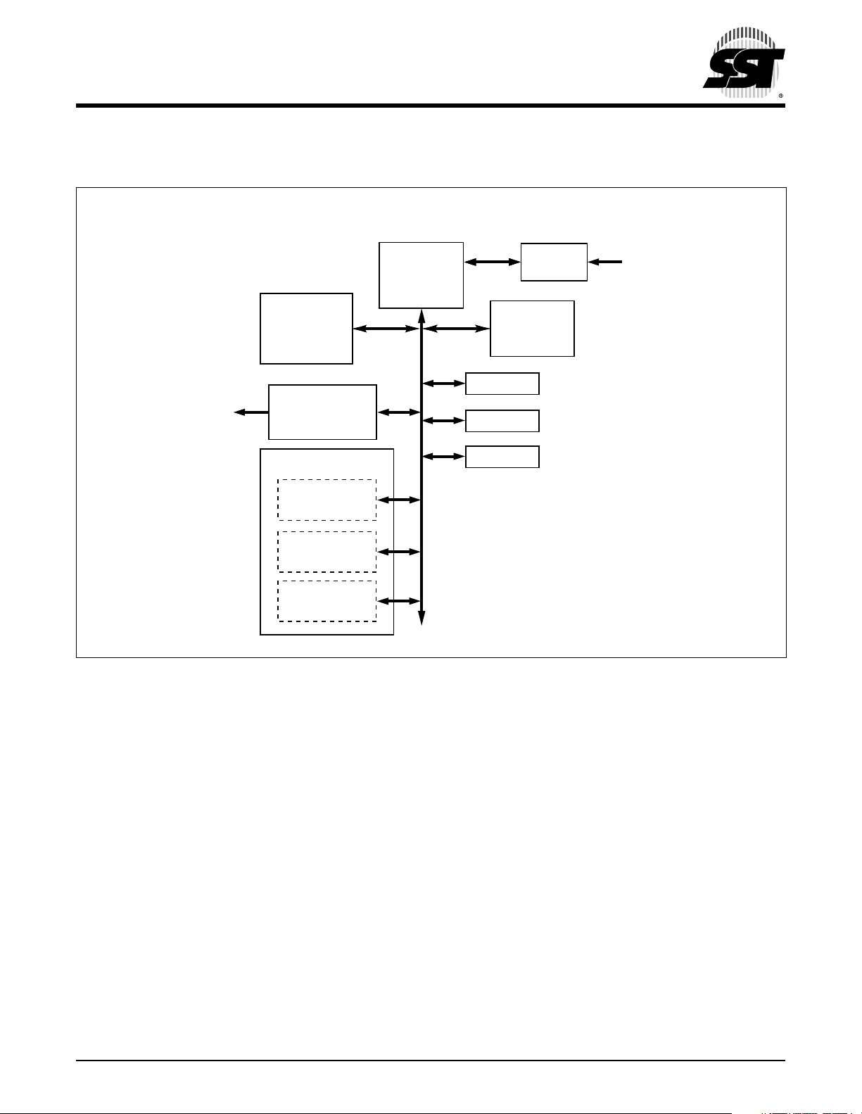
1.0 FUNCTIONAL BLOCKS
FUNCTIONAL BLOCK DIAGRAM
IRO
SuperFlash
Memory
16K x8
Carrier Modulator
Transmitter
Timer/Counter Interrupt
Real-Time
Counter
Core Timer
/ Counter
COP Watchdog
Timer
MCU Core
Por t A
Por t B
Por t C
Interrupt
Control
RAM
352K x8
IRQ#
368 ILL B1.8
©2001 Silicon Storage Technology, Inc. S71170-03-000 12/01 368
5
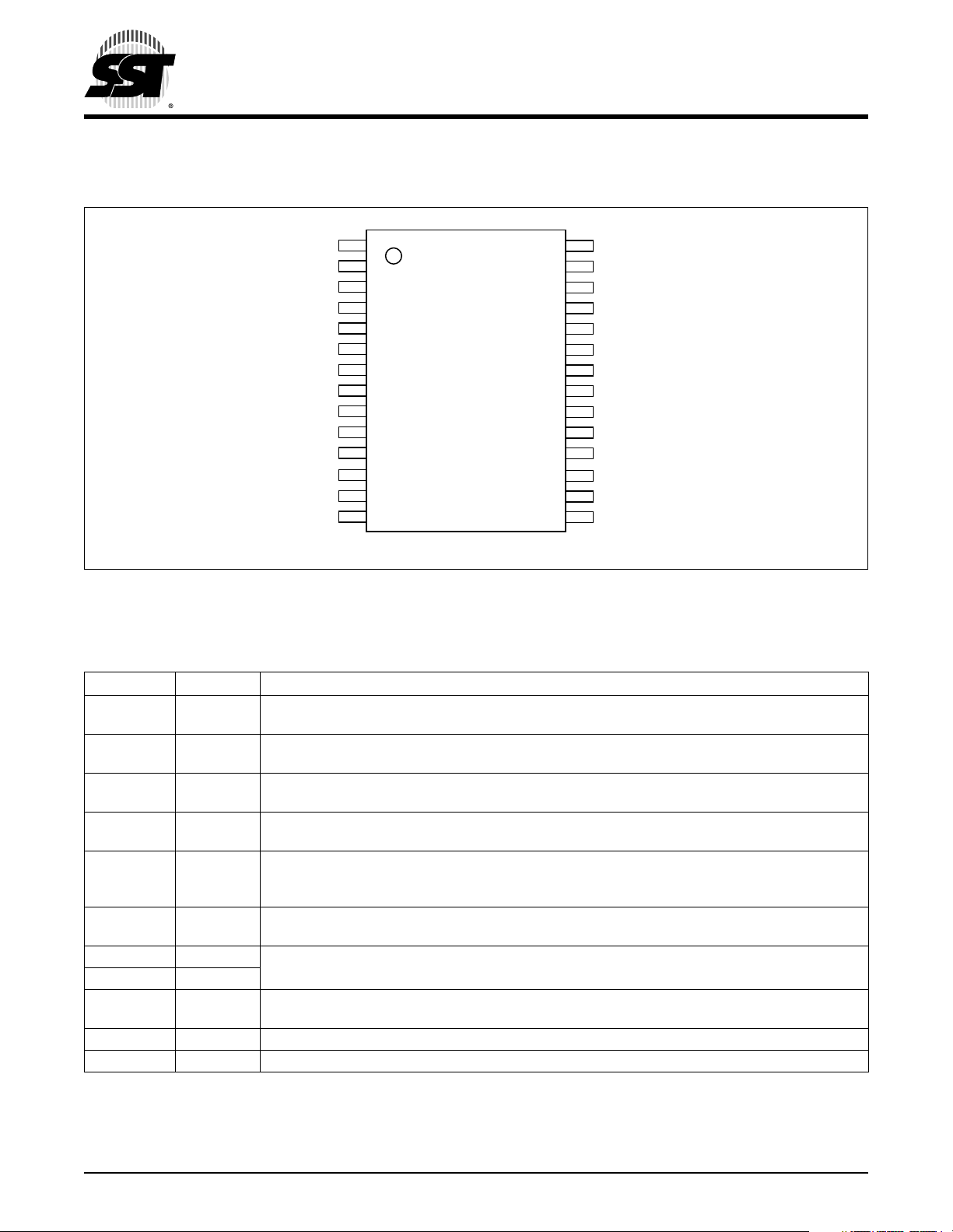
2.0 PIN ASSIGNMENTS
Remote Controller MCU
SST65P542R
Advance Information
PB0
PB1
PB2
PB3
PB4
PB5
PB6
PB7
PA 0
PA 1
PA 2
PA 3
PA 4
PA 5
1
2
3
4
5
6
7
8
9
10
11
12
13
14
28-lead SOIC
Top View
368 28-soic ILL P01.5
28
27
26
25
24
23
22
21
20
19
18
17
16
15
OSC1
OSC2
V
DD
IRQ#
RST#
IRO
V
SS
LPRST#
PC3
PC2
PC1
PC0
PA 7
PA 6
FIGURE 2-1: PIN ASSIGNMENTS FOR 28-LEAD SOIC
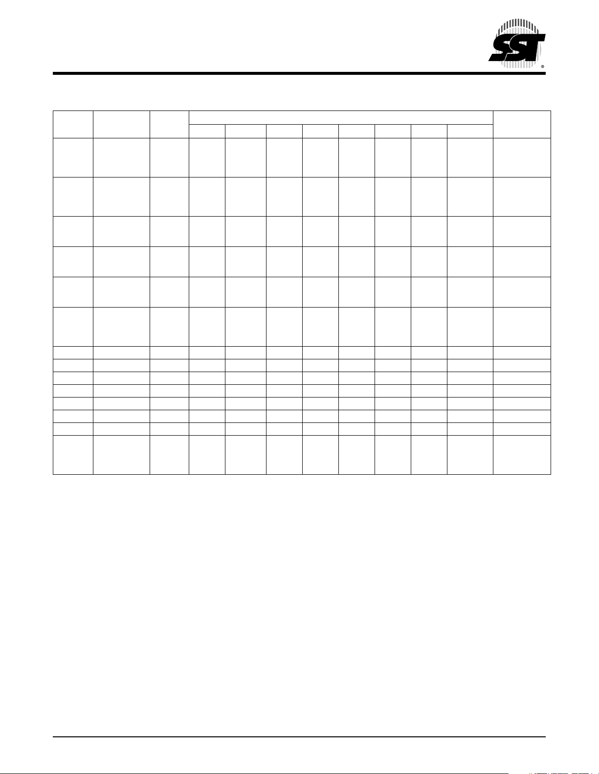
2.1 Pin Descriptions
TABLE 2-1: PIN DESCRIPTIONS
Symbol Type Name and Functions
PA[7:0] I/O
PB[7:0] I/O Por t B: The state of any pin in Port B is software programmable and every line is configured as an
PC[3:0] I/O Port C: Every pin in Port C is a high-current pin and its state is software programmable. All lines
IRO O IRO: Suitable for driving IR LED biasing logic, the IRO pin is the high-current source and sink out-
LPRST# I Low-Power Reset: An active-low pin, LPRST# function sets MCU to low-power reset mode. Once the
RST# I Reset: By setting the RST# pin low, the device is reset to a default state. An internal Schmitt trig-
OSC1 I Oscillator 1,2: These 2 pins interface with external oscillator circuits. A crystal
OSC2 O resonator, a ceramic resonator, or an external clock signal can be used.
IRQ# I Interrupt Request: The IRQ# is negative edge-sensitive triggered. An internal Schmitt trigger is
V
DD
V
SS
1. I = Input, O = Output
1
Port A: The state of any pin in Port A is software programmable and every line is configured as
an input during any reset.
input during any reset. Each I/O line contains a programmable interrupt/pull-up for keyscan.
are configured as inputs during any reset.
put of the carrier modulator transmitter subsystem. Default state is low after any reset.
device is in low-power reset mode, it is held in reset with all processor clocks and crystal oscillator halted.
An internal Schmitt trigger is included in the LPRST# pin to improve noise immunity.
ger is included in the RST# pin to improve noise immunity.
included in the IRQ# pin to improve noise immunity.
PWR Power Supply: Supply Voltage (2.2-3.2V)
PWR Ground: Circuit ground. (0V reference)
T2-1.14 368
©2001 Silicon Storage Technology, Inc. S71170-03-000 12/01 368
6
Remote Controller MCU
SST65P542R
Advance Information
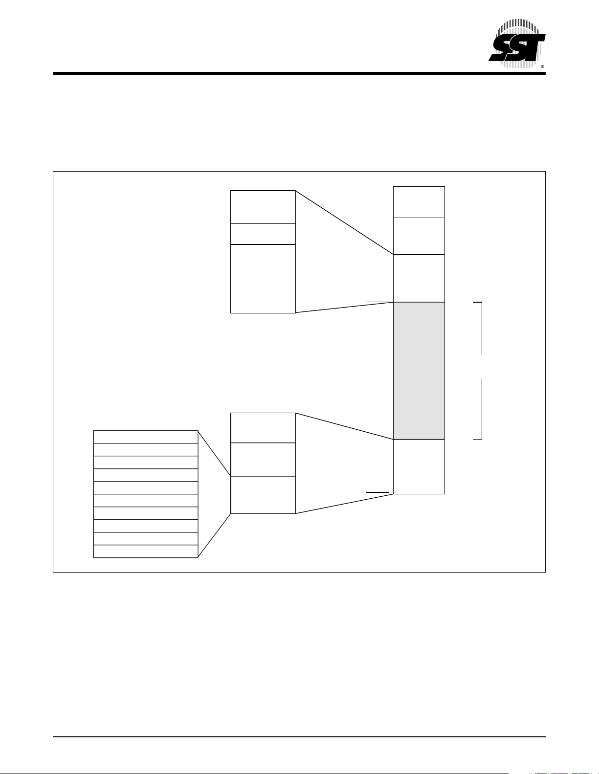
3.0 I/O REGISTERS AND MEMORY ORGANIZATION
The SST65P542R has a total of 64 KByte of addressable memory space. A memory map is located in Figure 3-1.
The on-chip memory consists of 32 Bytes of I/O registers, 352 Bytes of SRAM, 16 KByte of user flash memory and
128 Bytes of user vectors.
Core Timer Vector - (High Byte)
FFF6H
Core Timer Vector - (Low Byte)
FFF7H
FFF8H
FFF9H
FFFAH
FFFBH
FFFCH
FFFDH
FFFEH
FFFFH
CMT Vector (High Byte)
CMT Vector (Low Byte)
IRQ/Port B Vector (High Byte)
IRQ/Port B Vector (Low Byte)
SWI Vector (High Byte)
SWI Vector (Low Byte)
Reset Vector (High Byte)
Reset Vector (Low Byte)
Reserved
CWT Reset
Reserved
Flash Memory
Read Protection
Reserved
Reset and
Interrupt
Vectors
0180H
3FEFH
3FF0H
3FF1H
BFFFH
FF80H
FF81H
FFF5H
FFF6H
FFFFH
Flash Memory
(128 sectors)
I/O
Registers
352 Bytes
SRAM
User
Memory
16,256
Bytes
User
Vector
0000H
001FH
0020H
017FH
0180H
BFFFH
C000H
127 Sectors
(128 Bytes per sector)
FF7FH
FF80H
FFFFH
368 ILL F02.9
FIGURE 3-1: M
©2001 Silicon Storage Technology, Inc. S71170-03-000 12/01 368
EMORY MAP
7
Remote Controller MCU
SST65P542R
Advance Information
3.1 I/O Registers
The 32 Bytes of I/O registers occupy address locations from 0000H to 001FH that include general purpose I/O registers, the SuperFlash Function Register, and on-chip peripheral control registers.
TABLE 3-1: R
1
Symbol
PORTA Port A Data
PORTB Port B Data
PORTC Port C Data
DDRA Port A Data
DDRB Port B Data
DDRC Port C Data
CTSCR Core Timer
CTCR Core Timer
PBIC Port B
SFFR SuperFlash
PBPUC Port B Pull-up
CWTC CWT Control
CHR1 Carrier
CLR1 Carrier
CHR2 Carrier
Description
Register
Register
Register
- Reserved 0003H - - - - - - - - -
Direction
Register
Direction
Register
Direction
Register
- Reserved 0007H - - - - - - - - -
Control and
Status
Register
Counter
Register
Interrupt
Control
Register
Function
Register
Control
Register
Register
- Reserved 000EH - - - - - - - - -
- Reserved 000FH - - - - - - - - -
Generator
High Data
Register 1
Generator
Low Data
Register 1
Generator
High Data
Register 2
EGISTER DESCRIPTIONS AND BIT DEFINITIONS (1 OF 2)
Direct
Address
0000H PA7 PA6 PA5 PA4 PA3 PA2 PA1 PA0 00H
0001H PB7 PB6 PB5 PB4 PB3 PB2 PB1 PB0 00H
0002H - - - - PC3 PC2 PC1 PC0 00H
0004H DDRA7 DDRA6 DDRA5 DDRA4 DDRA3 DDRA2 DDRA1 DDRA0 00H
0005H DDRB7 DDRB6 DDRB5 DDRB4 DDRB3 DDRB2 DDRB1 DDRB0 00H
0006H - - - - DDRC3 DDRC2 DDRC1 DDRC0 00H
0008H CTOF RTIF TOFE RTIE TOFC RTFC RT1 RT0 03H
0009H CTD7 CTD6 CTD5 CTD4 CTD3 CTD2 CTD1 CTD0 00H
000AH INPRB7 INPRB6 INPRB5 INPRB4 INPRB3 INPRB2 INPRB1 INPRB0 00H
000BH PREN MEREN SEREN - PROG MERA SERA - 00H
000CH - - - - - - PU1 PU0 03H
000DH - - - - - - - CWT_EN 00000001b
0010H IROLN CMTPOL PH5 PH4 PH3 PH2 PH1 PH0 00UUUUUUb
0011H IROLP - PL5 PL4 PL3 PL2 PL1 PL0 00UUUUUUb
0012H - - SH5 SH4 SH3 SH2 SH1 SH0 00UUUUUUb
Bit 7 Bit 6 Bit 5 Bit 4 Bit 3 Bit 2 Bit 1 Bit 0
Bit Address, Bit Symbol
Reset
Val ue
2,3
©2001 Silicon Storage Technology, Inc. S71170-03-000 12/01 368
8
Remote Controller MCU
SST65P542R
Advance Information
TABLE 3-1: REGISTER DESCRIPTIONS AND BIT DEFINITIONS (CONTINUED) (2 OF 2)
1
Symbol
CLR2 Carrier
MCSR Modulator
MDR1 Modulator
MDR2 Modulator
MDR3 Modulator
PSCR Power
CWTC COP
1. “-” = reserved bits
2. “U” = unaffected by any reset
3. These registers can be reset by either external or internal reset.
Description
Generator
Low Data
Register 2
Control and
Status
Register
Data
Register 1
Data
Register 2
Data
Register 3
Saving
Control
Register
- Reserved 0019H - - - - - - - - -
- Reserved 001AH - - - - - - - - -
- Reserved 001BH - - - - - - - - -
- Reserved 001CH - - - - - - - - -
- Reserved 001DH - - - - - - - - -
- Reserved 001EH - - - - - - - - -
- Reserved 001FH - - - - - - - - -
Watchdog
Timer Reset
Register
Direct
Address
0013H - - SL5 SL4 SL3 SL2 SL1 SL0 00UUUUUUb
0014H EOC DIV2 EIMSK EXSPC BASE MODE EOCIE MCGEN 00H
0015H MB11 MB10 MB9 MB8 SB11 SB10 SB9 SB8 UUUUUUUUb
0016H MB7 MB6 MB5 MB4 MB3 MB2 MB1 MB0 UUUUUUUUb
0017H SB7 SB6 SB5 SB4 SB3 SB2 SB1 SB0 UUUUUUUUb
0018H EN - - - - - STOP IDL 10000011b
3FF0H - - - - - - - CWT_CLR 01H
Bit 7 Bit 6 Bit 5 Bit 4 Bit 3 Bit 2 Bit 1 Bit 0
Bit Address, Bit Symbol
Reset
Val ue
2,3
T3-1.8 368
©2001 Silicon Storage Technology, Inc. S71170-03-000 12/01 368
9
PORT A Data Register (PORTA)
Location
0000H
76543210
PA 7 PA 6 PA 5 PA 4 PA 3 PA 2 PA 1 PA 0
Symbol Function
PA[7:0] Port A data register bit 0 to 7. These bits are for both reading and writing. Write the data to this
register will output data to port A pins when it’s in output mode. If the pins are set to input mode,
only the output data register is updated, port A pins are tri-stated. Reading the data from this
register will read the state of port A pins when set in input mode. If the pins are set to output
mode, it reads the output data register. See Table 3-2 for details. For a detailed explanation of
each parallel I/O port, please refer to Section 4.0, “Parallel Input/Output Ports” on page 20.
PORT B Data Register (PORTB)
Location
0001H
76543210
PB7 PB6 PB5 PB4 PB3 PB2 PB1 PB0
Symbol Function
PB[7:0] Port B data register bit 0 to 7. These bits are for both reading and writing. Writing data to this
register will output data to port B pins when it’s in output mode. If the pins are set to input mode,
only the output data register is updated, port B pins are tri-stated. Reading the data from this
register will read the state of port B pins when set in input mode. If the pins are set to output
mode, it reads the output data register. See Table 3-2 for details.
Remote Controller MCU
SST65P542R
Advance Information
Reset Value
00H
Reset Value
00H
PORT C Data Register (PORTC)
Location
0003H
76543210
- - - - DDRC3 DDRC2 DDRC1 DDRC0
Symbol Function
PC[3:0] Port C data register bit 0 to 3. These bits are for both reading and writing. Writing data to this
register will output data to port C pins when it’s in output mode. If the pins are set to input mode,
only output data register is updated, port C pins are tri-stated. Reading data from this register will
read the state of port C pins when set in input mode. If the pins are set to output mode, it reads
the output data register. See Table 3-2 for details.
TABLE 3-2: I/O PIN FUNCTIONS AS GENERAL PURPOSE I/O
Access DDRA, DDRB, DDRC Mode I/O Pin Functions
Write 0 Input Data is written into the output data register.
Write 1 Output Data is written into the output data register and
Read 0 Input The state of I/O is read
Read 1 Output The output data register is read
Reset Value
00H
output to the I/O pins.
T3-2.0 368
©2001 Silicon Storage Technology, Inc. S71170-03-000 12/01 368
10
Remote Controller MCU
SST65P542R
Advance Information
PORT A Data Direction Register (DDRA)
Location
0004H
PORT B Data Direction Register (DDRB)
Location
0005H
76543210
DDRA7 DDRA6 DDRA5 DDRA4 DDRA3 DDRA2 DDRA1 DDRA0
Symbol Function
DDRA[7:0] Port A data direction register bit 0 to 7. These bits are for both reading and writing.
See Table 3-2 for details.
0: Port A is input
1: Port A is output
76543210
DDRB7 DDRB6 DDRB5 DDRB4 DDRB3 DDRB2 DDRB1 DDRB0
Symbol Function
DDRB[7:0] Port B data direction register bit 0 to 7. These bits are for both reading and writing.
See Table 3-2 for details.
0: Port B is input
1: Port B is output
Reset Value
00H
Reset Value
00H
PORT C Data Direction Register (DDRC)
Location
0006H
76543210
----PC3PC2PC1PC0
Symbol Function
DDRC[3:0] Port C data direction register bit 0 to 3. These bits are for both reading and writing.
See Table 3-2 for details.
0: Port C is input
1: Port C is output
PORT B Interrupt Control Register (PBIC)
Location
000AH
76543210
INPRB7 INPRB6 INPRB5 INPRB4 INPRB3 INPRB2 INPRB1 INPRB0
Symbol Function
INPRB[7:0] Port B interrupt control bits
0: Interrupt is enabled
1: Interrupt is disabled
Reset Value
00H
Reset Value
00H
©2001 Silicon Storage Technology, Inc. S71170-03-000 12/01 368
11
PORT B Pull-up Control Register (PBPUC)
Location
000CH
76543210
------PU1PU0
Symbol Function
PU1,PU0 Port B pull-up control bits. The following table shows pull-up strength.
Defaults to strong pull-up when reset.
TABLE 3-3: PULL-UP CONTROL BIT DESCRIPTION
PU1 PU0 Pull-up
0 0 No pull-up for Port B bit
0 1 Weak pull-up for each Port B bit
1 0 Weak pull-up for each Port B bit
1 1 Strong pull-up for each Port B bit
1. Default value after Power-on or Reset
Remote Controller MCU
SST65P542R
Advance Information
Reset Value
03H
1
T3-3.1 368
©2001 Silicon Storage Technology, Inc. S71170-03-000 12/01 368
12
 Loading...