

Silicon Storage Technology Inc SST58LD008-70-C-P1H, SST58SD192-70-C-P1H, SST58SD128-70-C-P1H, SST58SD096-70-C-P1H, SST58SD064-70-C-P1H Datasheet
...
ATA-Disk Chip
SST58SD008 / 016 / 024 / 032 / 048 / 064 / 096 / 128 / 192
SST58LD008 / 016 / 024 / 032 / 048 / 064 / 096 / 128 / 192
8MB / 16MB / 24MB / 32MB / 48MB / 64MB / 96MB / 128MB / 192MB
SST58SD/LDxxxATA-Disk Chip
FEATURES:
• ATA/IDE standard interface
– 512 Bytes per sector
– ATA command set compatible
– Support Data Transfer Speed up to PIO Mode-4
• 8, 16, 24, 32, 48, 64, 96, 128, and 192 MByte
capacities
• 600 mil 32-pin DIP package
• Single Voltage Read and Write Operation
– 5.0V-only for SST58SDxxx
– 3.3V-only for SST58LDxxx
• Supports 5.0-Volt or 3.3-Volt Read and Write
– 4.5-5.5V or 3.135-3.465V for Commercial
• Low Power Consumption
– Active mode: 35 mA/55 mA (3.3V/5.0V)(typical)
– Sleep mode: 100 µA/150 µA (3.3V/5.0V)(typical)
• Extended Data Protection and Security
– WP# pin for Dat a Protection
– Factory-Programmed, 20-Byte Unique ID number
• Sustained Write Performance
– Up to 1.4 MB/sec (host to flash)
Data Sheet
• Controller Overhead Command to DRQ
– Less than 0.5 ms
• Zero Power Data Retention
– Batteries not required for data storage
•Start Up Time
– Sleep to read: 200 ns (typical)
– Sleep to write: 200 ns (typical)
– Power-on to Ready:200 ms (typical)
• Support for Commercial Temperature Range
– 0°C to +70°C for Operating Commercial
– -50°C to +100°C for non-Operating (storage)
• Extremely Rugged and Reliable
– Built-in ECC support corrects 3 Bytes of error
per 512 Byte sector
• Intelligent ATA/IDE Controller
– Built-in microcontroller with intelligent firmware
– Built-in Embedded Flash File System
• Power Management Unit
– Immediate disabling of unused circuitry
PRODUCT DESCRIPTION
SST’s ATA-Disk Chip (ADC) is a low cost, high performance, embedded flash memory data storage system.
This product is well suited for solid state mass storage
applications of fering new a nd expanded f un ctional ity whil e
enabling cost effective designs.
ATA-based solid state mass storage technology is widely
used in such products as portable and desktop computers,
digital cameras, music players, handheld data collection
scanners, cell ular phones , PCS pho nes, PD As , handy terminals, personal communicators, advanced two-way pagers,
audio recorders, monitoring devices, and set-top boxes.
ADC provides comple te IDE Hard Disk Drive functionali ty
and compatibility. ADC is a perfect solution to consum er
electronic products requiring smaller, but more reliable and
cost effe ct i ve data storage. The ADC is re ad an d writ ten to
using a single power supply of 5.0V or 3.3V and is available
in 8 to 192 MByte capacities.
The ADC is a solid state disk drive that is designed to
replace conventional IDE hard disk dr ive and uses standard ATA/IDE protocol . It h as b uilt i n microc ontrol ler and file
management fir mware that communicates with ATA stan-
dard interfaces; therefore, the ADC does not require additional or propr ietary software such as Flash File System
(FFS) and Memory Technology Driv er (MTD) softw are .
The ADC is designed to work at either 5V or 3.3V. The pin
assignment is designed to match existing IDE signal traces
on the motherboard. It uses standard AT A driver that is part
of all major OS such as Windows 95/98/2000/NT/CE,
MAC, UNIX, etc.
All signals, except WP #, are in compliance wi th the ATA
specifications. WP# is used to write protect the information
stored on the ADC. The WP# ca n be either conn ected to
motherboard write protect control logic or a jumper. When
WP# is low, the ADC is write protected to prohibit any inadvertent writes.
Every ADC comes with factory-programmed, 20-Byte long,
unique identific ation number for extended data protection .
This feature prevents unauthorized duplic ation by allow ing
encryption of customer data.
The ADC is packaged in the 600 mil 32-pin DIP package
for easy and cost effective mounting to the system motherboard.
©2001 Silicon Storage Technology, Inc.
S71167-05-000 9/01 391
1
The SST logo and SuperFlash are registered trademarks of Silicon Storage Technology, Inc.
ATA-Disk Chip is a trademark of Silicon Storage Tech nology, Inc.
These specifications are subject to change without notice.

ATA-Disk Chip
SST58SD008 / 016 / 024 / 032 / 048 / 064 / 096 / 128 / 192
SST58LD008 / 016 / 024 / 032 / 048 / 064 / 096 / 128 / 192
Data Sheet
TABLE OF CONTENTS
PRODUCT DESCRIPTION . . . . . . . . . . . . . . . . . . . . . . . . . . . . . . . . . . . . . . . . . . . . . . . . . . . . . . . . . . . . . . . . . . . 1
1.0 GENERAL DESCRIPTION . . . . . . . . . . . . . . . . . . . . . . . . . . . . . . . . . . . . . . . . . . . . . . . . . . . . . . . . . . . . . . . 5
1.1 Performance-optimized ATA Controller . . . . . . . . . . . . . . . . . . . . . . . . . . . . . . . . . . . . . . . . . . . . . . . . . . 5
1.1.1 Microcontroller Unit (MCU). . . . . . . . . . . . . . . . . . . . . . . . . . . . . . . . . . . . . . . . . . . . . . . . . . . . . . . 5
1.1.2 Internal Direct Memory Access (DMA). . . . . . . . . . . . . . . . . . . . . . . . . . . . . . . . . . . . . . . . . . . . . . 5
1.1.3 Power Management Unit (PMU) . . . . . . . . . . . . . . . . . . . . . . . . . . . . . . . . . . . . . . . . . . . . . . . . . . 5
1.1.4 SRAM Buffer . . . . . . . . . . . . . . . . . . . . . . . . . . . . . . . . . . . . . . . . . . . . . . . . . . . . . . . . . . . . . . . . . 5
1.1.5 Embedded Flash File System . . . . . . . . . . . . . . . . . . . . . . . . . . . . . . . . . . . . . . . . . . . . . . . . . . . . 5
1.1.6 Error Correction Code (ECC). . . . . . . . . . . . . . . . . . . . . . . . . . . . . . . . . . . . . . . . . . . . . . . . . . . . . 5
1.2 SST’s ATA-Disk Chip Product Offering . . . . . . . . . . . . . . . . . . . . . . . . . . . . . . . . . . . . . . . . . . . . . . . . . . 6
2.0 ELECTRICAL INTERFACE . . . . . . . . . . . . . . . . . . . . . . . . . . . . . . . . . . . . . . . . . . . . . . . . . . . . . . . . . . . . . . 6
2.0.1 Pin Assignment and Pin Type . . . . . . . . . . . . . . . . . . . . . . . . . . . . . . . . . . . . . . . . . . . . . . . . . . . . 6
2.1 Electrical Description . . . . . . . . . . . . . . . . . . . . . . . . . . . . . . . . . . . . . . . . . . . . . . . . . . . . . . . . . . . . . . . . 6
2.2 Absolute Maximum Stress Ratings . . . . . . . . . . . . . . . . . . . . . . . . . . . . . . . . . . . . . . . . . . . . . . . . . . . . . 9
2.3 Electrical Specification . . . . . . . . . . . . . . . . . . . . . . . . . . . . . . . . . . . . . . . . . . . . . . . . . . . . . . . . . . . . . . 10
2.3.1 Absolute Maximum Conditions. . . . . . . . . . . . . . . . . . . . . . . . . . . . . . . . . . . . . . . . . . . . . . . . . . . 10
2.3.2 Input Leakage Current . . . . . . . . . . . . . . . . . . . . . . . . . . . . . . . . . . . . . . . . . . . . . . . . . . . . . . . . . 10
2.3.3 Input Characteristics. . . . . . . . . . . . . . . . . . . . . . . . . . . . . . . . . . . . . . . . . . . . . . . . . . . . . . . . . . . 11
2.3.4 Output Drive Type . . . . . . . . . . . . . . . . . . . . . . . . . . . . . . . . . . . . . . . . . . . . . . . . . . . . . . . . . . . . 11
2.3.5 Output Drive Characteristics . . . . . . . . . . . . . . . . . . . . . . . . . . . . . . . . . . . . . . . . . . . . . . . . . . . . 11
2.3.6 I/O Input (Read) Timing Specification . . . . . . . . . . . . . . . . . . . . . . . . . . . . . . . . . . . . . . . . . . . . . 12
2.3.7 I/O Output (Write) Timing Specification . . . . . . . . . . . . . . . . . . . . . . . . . . . . . . . . . . . . . . . . . . . . 13
2.4 I/O Transfer Function. . . . . . . . . . . . . . . . . . . . . . . . . . . . . . . . . . . . . . . . . . . . . . . . . . . . . . . . . . . . . . . 14
2.4.1 I/O Function . . . . . . . . . . . . . . . . . . . . . . . . . . . . . . . . . . . . . . . . . . . . . . . . . . . . . . . . . . . . . . . . . 14
3.0 SOFTWARE INTERFACE . . . . . . . . . . . . . . . . . . . . . . . . . . . . . . . . . . . . . . . . . . . . . . . . . . . . . . . . . . . . . . 15
3.1 ATA-Disk Chip Drive Register Set Definitions and Protocol . . . . . . . . . . . . . . . . . . . . . . . . . . . . . . . . . 15
3.1.1 ATA-Disk Chip Addressing. . . . . . . . . . . . . . . . . . . . . . . . . . . . . . . . . . . . . . . . . . . . . . . . . . . . . . 15
3.1.2 ATA-Disk Chip Registers . . . . . . . . . . . . . . . . . . . . . . . . . . . . . . . . . . . . . . . . . . . . . . . . . . . . . . . 15
3.1.2.1 Data Register . . . . . . . . . . . . . . . . . . . . . . . . . . . . . . . . . . . . . . . . . . . . . . . . . . . . . . . . . 15
3.1.2.2 Error Register (Read Only) . . . . . . . . . . . . . . . . . . . . . . . . . . . . . . . . . . . . . . . . . . . . . . . 15
3.1.2.3 Feature Register (Write Only) . . . . . . . . . . . . . . . . . . . . . . . . . . . . . . . . . . . . . . . . . . . . . 16
3.1.2.4 Sector Count Register. . . . . . . . . . . . . . . . . . . . . . . . . . . . . . . . . . . . . . . . . . . . . . . . . . . 16
3.1.2.5 Sector Number (LBA 7-0) Register . . . . . . . . . . . . . . . . . . . . . . . . . . . . . . . . . . . . . . . . . 16
3.1.2.6 Cylinder Low (LBA 15-8) Register. . . . . . . . . . . . . . . . . . . . . . . . . . . . . . . . . . . . . . . . . . 16
3.1.2.7 Cylinder High (LBA 23-16) Register . . . . . . . . . . . . . . . . . . . . . . . . . . . . . . . . . . . . . . . . 16
3.1.2.8 Drive/Head (LBA 27-24) Register . . . . . . . . . . . . . . . . . . . . . . . . . . . . . . . . . . . . . . . . . . 16
3.1.2.9 Status & Alternate Status Registers (Read Only) . . . . . . . . . . . . . . . . . . . . . . . . . . . . . . 17
3.1.2.10 Device Control Register (Write Only) . . . . . . . . . . . . . . . . . . . . . . . . . . . . . . . . . . . . . . 17
3.1.2.11 Drive Address Register (Read Only). . . . . . . . . . . . . . . . . . . . . . . . . . . . . . . . . . . . . . . 18
3.1.2.12 Command Register (Write Only) . . . . . . . . . . . . . . . . . . . . . . . . . . . . . . . . . . . . . . . . . . 18
©2001 Silicon Storage Technology, Inc. S71167-05-000 9/01 391
2

ATA-Disk Chip
SST58SD008 / 016 / 024 / 032 / 048 / 064 / 096 / 128 / 192
SST58LD008 / 016 / 024 / 032 / 048 / 064 / 096 / 128 / 192
Data Sheet
3.2 ATA-Disk Chip Command Description. . . . . . . . . . . . . . . . . . . . . . . . . . . . . . . . . . . . . . . . . . . . . . . . . . 19
3.2.1 ATA-Disk Chip Command Set . . . . . . . . . . . . . . . . . . . . . . . . . . . . . . . . . . . . . . . . . . . . . . . . . . . 19
3.2.1.1 Check Power Mode - 98H or E5H. . . . . . . . . . . . . . . . . . . . . . . . . . . . . . . . . . . . . . . . . . 20
3.2.1.2 Execute Drive Diagnostic - 90H . . . . . . . . . . . . . . . . . . . . . . . . . . . . . . . . . . . . . . . . . . . 20
3.2.1.3 Format Track - 50H. . . . . . . . . . . . . . . . . . . . . . . . . . . . . . . . . . . . . . . . . . . . . . . . . . . . . 21
3.2.1.4 Identify Drive - ECH. . . . . . . . . . . . . . . . . . . . . . . . . . . . . . . . . . . . . . . . . . . . . . . . . . . . . 21
3.2.1.4.1 General Configuration. . . . . . . . . . . . . . . . . . . . . . . . . . . . . . . . . . . . . . . . . . . . 23
3.2.1.4.2 Default Number of Cylinders. . . . . . . . . . . . . . . . . . . . . . . . . . . . . . . . . . . . . . . 23
3.2.1.4.3 Default Number of Heads. . . . . . . . . . . . . . . . . . . . . . . . . . . . . . . . . . . . . . . . . 23
3.2.1.4.4 Default Number of Sectors per Track . . . . . . . . . . . . . . . . . . . . . . . . . . . . . . . . 23
3.2.1.4.5 Number of Sectors . . . . . . . . . . . . . . . . . . . . . . . . . . . . . . . . . . . . . . . . . . . . . . 23
3.2.1.4.6 Memory Serial Number. . . . . . . . . . . . . . . . . . . . . . . . . . . . . . . . . . . . . . . . . . . 23
3.2.1.4.7 Buffer Type. . . . . . . . . . . . . . . . . . . . . . . . . . . . . . . . . . . . . . . . . . . . . . . . . . . . 23
3.2.1.4.8 Buffer Size . . . . . . . . . . . . . . . . . . . . . . . . . . . . . . . . . . . . . . . . . . . . . . . . . . . . 23
3.2.1.4.9 ECC Count . . . . . . . . . . . . . . . . . . . . . . . . . . . . . . . . . . . . . . . . . . . . . . . . . . . . 23
3.2.1.4.10 Firmware Revision . . . . . . . . . . . . . . . . . . . . . . . . . . . . . . . . . . . . . . . . . . . . . 23
3.2.1.4.11 Model Number . . . . . . . . . . . . . . . . . . . . . . . . . . . . . . . . . . . . . . . . . . . . . . . . 23
3.2.1.4.12 Read/Write Multiple Sector Count . . . . . . . . . . . . . . . . . . . . . . . . . . . . . . . . . 23
3.2.1.4.13 Capabilities. . . . . . . . . . . . . . . . . . . . . . . . . . . . . . . . . . . . . . . . . . . . . . . . . . . 23
3.2.1.4.14 PIO Data Transfer Cycle Timing Mode. . . . . . . . . . . . . . . . . . . . . . . . . . . . . . 24
3.2.1.4.15 Translation Parameters Valid . . . . . . . . . . . . . . . . . . . . . . . . . . . . . . . . . . . . . 24
3.2.1.4.16 Current Number of Cylinders, Heads, Sectors/Track . . . . . . . . . . . . . . . . . . . 24
3.2.1.4.17 Current Capacity. . . . . . . . . . . . . . . . . . . . . . . . . . . . . . . . . . . . . . . . . . . . . . . 24
3.2.1.4.18 Multiple Sector Setting . . . . . . . . . . . . . . . . . . . . . . . . . . . . . . . . . . . . . . . . . . 24
3.2.1.4.19 Total Sectors Addressable in LBA Mode . . . . . . . . . . . . . . . . . . . . . . . . . . . . 24
3.2.1.4.20 Advanced PIO Data Transfer Mode . . . . . . . . . . . . . . . . . . . . . . . . . . . . . . . . 24
3.2.1.4.21 Minimum PIO Transfer Cycle Time Without Flow Control . . . . . . . . . . . . . . . 24
3.2.1.4.22 Minimum PIO Transfer Cycle Time With IORDY . . . . . . . . . . . . . . . . . . . . . . 24
3.2.1.5 Idle - 97H or E3H. . . . . . . . . . . . . . . . . . . . . . . . . . . . . . . . . . . . . . . . . . . . . . . . . . . . . . . 24
3.2.1.6 Idle Immediate - 95H or E1H. . . . . . . . . . . . . . . . . . . . . . . . . . . . . . . . . . . . . . . . . . . . . . 25
3.2.1.7 Initialize Drive Parameters - 91H. . . . . . . . . . . . . . . . . . . . . . . . . . . . . . . . . . . . . . . . . . . 25
3.2.1.8 Read Buffer - E4H. . . . . . . . . . . . . . . . . . . . . . . . . . . . . . . . . . . . . . . . . . . . . . . . . . . . . . 25
3.2.1.9 Read Multiple - C4H . . . . . . . . . . . . . . . . . . . . . . . . . . . . . . . . . . . . . . . . . . . . . . . . . . . . 26
3.2.1.10 Read Long Sector - 22H or 23H . . . . . . . . . . . . . . . . . . . . . . . . . . . . . . . . . . . . . . . . . . 27
3.2.1.11 Read Sectors - 20H or 21H. . . . . . . . . . . . . . . . . . . . . . . . . . . . . . . . . . . . . . . . . . . . . . 27
3.2.1.12 Read Verify Sector(s) - 40H or 41H . . . . . . . . . . . . . . . . . . . . . . . . . . . . . . . . . . . . . . . 28
3.2.1.13 Recalibrate - 1XH . . . . . . . . . . . . . . . . . . . . . . . . . . . . . . . . . . . . . . . . . . . . . . . . . . . . . 28
3.2.1.14 Seek - 7XH . . . . . . . . . . . . . . . . . . . . . . . . . . . . . . . . . . . . . . . . . . . . . . . . . . . . . . . . . . 28
3.2.1.15 Set Features - EFH . . . . . . . . . . . . . . . . . . . . . . . . . . . . . . . . . . . . . . . . . . . . . . . . . . . . 29
3.2.1.16 Set Multiple Mode - C6H . . . . . . . . . . . . . . . . . . . . . . . . . . . . . . . . . . . . . . . . . . . . . . . . 30
3.2.1.17 Set Sleep Mode - 99H or E6H. . . . . . . . . . . . . . . . . . . . . . . . . . . . . . . . . . . . . . . . . . . . 30
3.2.1.18 Standby - 96H or E2H. . . . . . . . . . . . . . . . . . . . . . . . . . . . . . . . . . . . . . . . . . . . . . . . . . 31
3.2.1.19 Standby Immediate - 94H or E0H . . . . . . . . . . . . . . . . . . . . . . . . . . . . . . . . . . . . . . . . . 31
3.2.1.20 Write Buffer - E8H. . . . . . . . . . . . . . . . . . . . . . . . . . . . . . . . . . . . . . . . . . . . . . . . . . . . . 31
3.2.1.21 Write Long Sector - 32H or 33H . . . . . . . . . . . . . . . . . . . . . . . . . . . . . . . . . . . . . . . . . . 32
3.2.1.22 Write Multiple Command - C5H. . . . . . . . . . . . . . . . . . . . . . . . . . . . . . . . . . . . . . . . . . . 32
3.2.1.23 Write Sector(s) - 30H or 31H. . . . . . . . . . . . . . . . . . . . . . . . . . . . . . . . . . . . . . . . . . . . . 33
3.2.1.24 Write Verify - 3CH . . . . . . . . . . . . . . . . . . . . . . . . . . . . . . . . . . . . . . . . . . . . . . . . . . . . . 33
3.2.2 Error Posting . . . . . . . . . . . . . . . . . . . . . . . . . . . . . . . . . . . . . . . . . . . . . . . . . . . . . . . . . . . . . . . . 34
©2001 Silicon Storage Technology, Inc. S71167-05-000 9/01 391
3

ATA-Disk Chip
SST58SD008 / 016 / 024 / 032 / 048 / 064 / 096 / 128 / 192
SST58LD008 / 016 / 024 / 032 / 048 / 064 / 096 / 128 / 192
Data Sheet
4.0 APPENDIX . . . . . . . . . . . . . . . . . . . . . . . . . . . . . . . . . . . . . . . . . . . . . . . . . . . . . . . . . . . . . . . . . . . . . . . . . . 35
4.1 Differences between ATA-Disk Chip and ATA/ATAPI-5 Specifications. . . . . . . . . . . . . . . . . . . . . . . . . 35
4.1.1 Electrical Differences . . . . . . . . . . . . . . . . . . . . . . . . . . . . . . . . . . . . . . . . . . . . . . . . . . . . . . . . . . 35
4.1.1.1 TTL Compatibility . . . . . . . . . . . . . . . . . . . . . . . . . . . . . . . . . . . . . . . . . . . . . . . . . . . . . . 35
4.1.1.2 Pull Up Resistor Input Leakage Current . . . . . . . . . . . . . . . . . . . . . . . . . . . . . . . . . . . . . 35
4.1.2 Functional Differences . . . . . . . . . . . . . . . . . . . . . . . . . . . . . . . . . . . . . . . . . . . . . . . . . . . . . . . . . 35
4.1.2.1 Idle Timer . . . . . . . . . . . . . . . . . . . . . . . . . . . . . . . . . . . . . . . . . . . . . . . . . . . . . . . . . . . . 35
4.1.2.2 Recovery from Sleep Mode. . . . . . . . . . . . . . . . . . . . . . . . . . . . . . . . . . . . . . . . . . . . . . . 35
5.0 PHYSICAL DIMENSIONS . . . . . . . . . . . . . . . . . . . . . . . . . . . . . . . . . . . . . . . . . . . . . . . . . . . . . . . . . . . . . . 36
6.0 PRODUCT ORDERING INFORMATION . . . . . . . . . . . . . . . . . . . . . . . . . . . . . . . . . . . . . . . . . . . . . . . . . . . 37
6.1 Valid Combinations . . . . . . . . . . . . . . . . . . . . . . . . . . . . . . . . . . . . . . . . . . . . . . . . . . . . . . . . . . . . . . . . 38
7.0 LIMITED WARRANTY . . . . . . . . . . . . . . . . . . . . . . . . . . . . . . . . . . . . . . . . . . . . . . . . . . . . . . . . . . . . . . . . . 39
7.1 Life Support Policy. . . . . . . . . . . . . . . . . . . . . . . . . . . . . . . . . . . . . . . . . . . . . . . . . . . . . . . . . . . . . . . . . 39
7.2 Patent Protection . . . . . . . . . . . . . . . . . . . . . . . . . . . . . . . . . . . . . . . . . . . . . . . . . . . . . . . . . . . . . . . . . . 39
©2001 Silicon Storage Technology, Inc. S71167-05-000 9/01 391
4
ATA-Disk Chip
SST58SD008 / 016 / 024 / 032 / 048 / 064 / 096 / 128 / 192
SST58LD008 / 016 / 024 / 032 / 048 / 064 / 096 / 128 / 192
Data Sheet
1.0 GENERAL DESCRIPTION
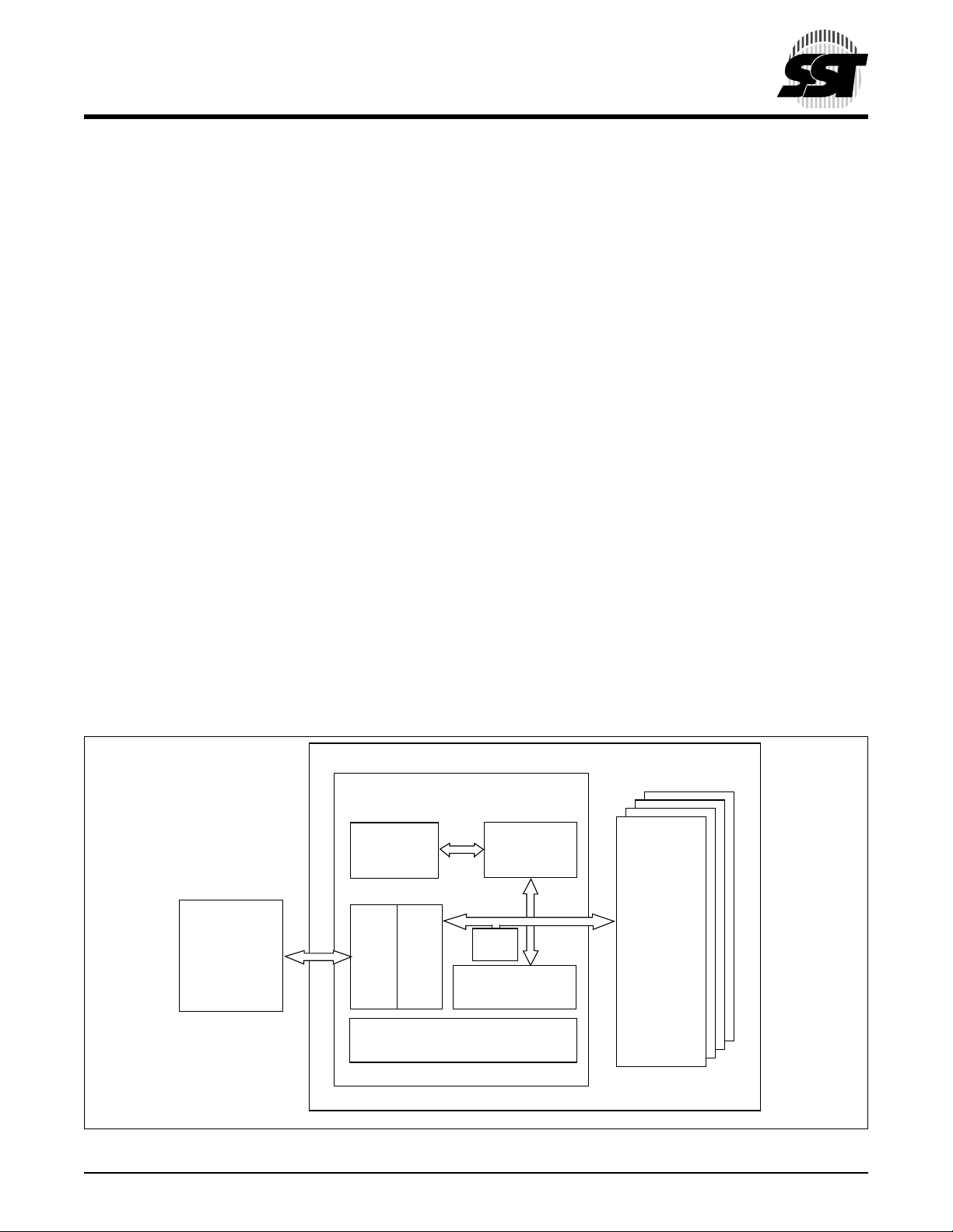
The SST’s ATA-Disk Chip (ADC) contains a controller,
embedded firmware and Flash Media in a 32-pin DIP package. Refer to Figure 1-1 for SST’s ADC block diagram. The
controller interfaces with the host system allowing data to
be written to and read from the Flash Media.
1.1 Performance-optimized ATA Controller
The heart of the ADC is the AT A controller which translates
standard ATA signals into Flas h Media data an d controls.
SST’s ADC contains a propr ietar y ATA controller that was
specifically designed to attain high data throughput from
host to Flash. The following co mponents cont ribute to the
ATA controller’ s ope rati on.
1.1.1 Microcontroller Unit (MCU)
The MCU translates ATA command s into data an d control
signals required for flash memory operation.
1.1.2 Internal Direct Memory Access (DMA)
The ATA controller inside ADC uses DMA allowing instant
data transfer from buffer to memory. This implementation
eliminates microc ontroller overhead associated with traditional, firmware based, memory control, increasing data
transfer rate.
1.1.3 Power Management Unit (PMU)
Power Management Unit control s the power c onsumptio n
of the ADC. The PMU dramatically extends product battery
life by putting the part of the circuitry that is not in operation
into sleep mode.
1.1.4 SRAM Buffer
A key contributor to the ATA controller performance is an
SRAM buffer. The buffer optimizes host’s data writes to
Flash Media.
1.1.5 Embedded Flash File System
Embedded Flash File System is an integral part of the
SST’s ATA controller. It contains MCU Firmware that performs the f ollow ing tasks:
1. Translates host side signals into Flash Media
Writes and Reads.
2. Provides Flash Media wear leveling to spread the
Flash writes across all the memory address space
to increase the longevity of Flash Media.
3. Keeps track of data file structures.
1.1.6 Error Correction Code (ECC)
The ATA Controller contain s E CC algori th m th at c o rr ec t s
3 Bytes of error pe r 512 Byte se cto r.
ATA Controller
Embedded
Flash
File System
SRAM Buffer
HOST
ATA/IDE
BUS
PMU
FIGURE 1-1: SST ATA-D
©2001 Silicon Storage Technology, Inc. S71167-05-000 9/01 391
ISK CHIP BLOCK DIAGRAM
ECC
5
MCU
Flash
Media
Internal
DMA
391 ILL1-1.5
ATA-Disk Chip
SST58SD008 / 016 / 024 / 032 / 048 / 064 / 096 / 128 / 192
SST58LD008 / 016 / 024 / 032 / 048 / 064 / 096 / 128 / 192
Data Sheet
1.2 SST’s ATA-Disk Chip Product Offering
The SST58SD/LDxxx ATA-Disk Chip product family is available in 8 to 192 MByte capacities. The following table
shows the specific capacity, default number of cylinder heads, sectors and cylinders for each product line.
Model Number Density T ota l Bytes Cylinders Heads Sectors
SST58SD/LD008 8 MB 8,028,160 245 2 32
SST58SD/LD016 16 MB 16,023,552 489 2 32
SST58SD/LD024 24 MB 24,051,712 367 4 32
SST58SD/LD032 32 MB 32,047,104 489 4 32
SST58SD/LD048 48 MB 48,037,888 733 4 32
SST58SD/LD064 64 MB 64,028,672 977 4 32
SST58SD/LD096 96 MB 96,075,776 733 8 32
SST58SD/LD128 128 MB 128,057 ,344 977 8 32
SST58SD/LD192 192 MB 192,151 ,552 733 16 3 2
2.0 ELECTRICAL INTERFACE
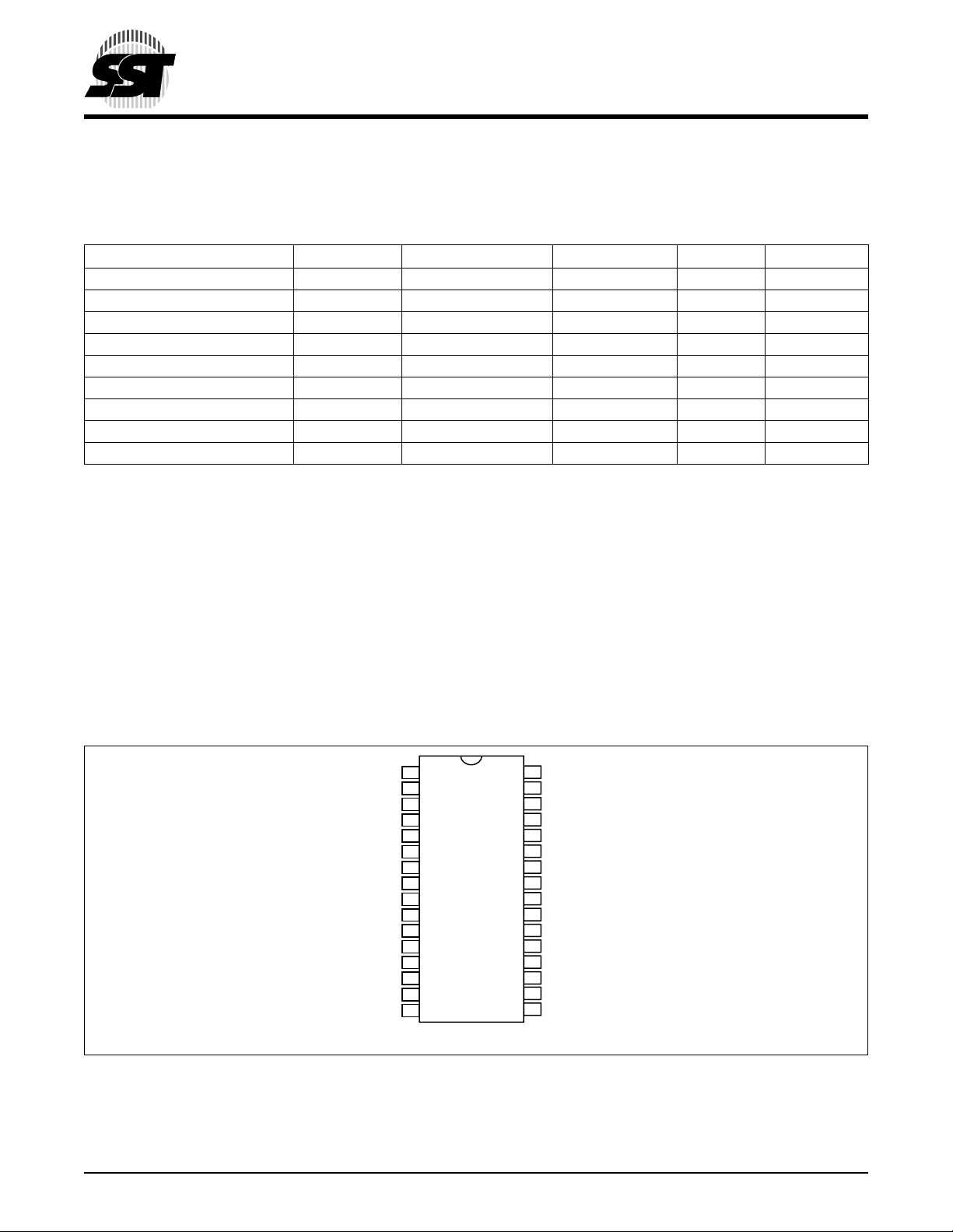
2.0.1 Pin Assignment and Pin Type
The signal/pin assignments are listed in Table 2-1. Low active signals have a “#” suffix. Pin types are Input, Output or Input/
Output. Section 2.3 defines the DC characteristics for all input and output type structures.
2.1 Electrical Description
The ADC functions in A TA Mode, which is compatible with IDE hard disk drives.
Table 2-2 descr ibes the I/O sign als. Signa ls who se sour ce is t he hos t are des igna ted as input s whil e signa ls tha t the AD C
sources are ou tputs. All outputs from the ADC are totem pole except the data bus signals which are in the bi-dir ectional tristate. Refer to Section 2.3.2 for definitions of Input and Output types.
RESET#
D7
D6
D5
D4
D3
D2
D1
D0
WP#
IORD#
INTRQ
A1
A0
CS1FX#
GND
1
2
3
4
5
6
7
8
9
10
11
12
13
14
15
16
32-pin
PSDIP
T op Vie w
32
V
31
30
29
28
27
26
25
24
23
22
21
20
19
18
17
CC
D8
D9
D10
D11
D12
D13
D14
D15
IOWR#
CSEL
IOCS16#
PDIAG#
A2
CS3FX#
DASP#
391 ILL F01.5
FIGURE 2-1: P
©2001 Silicon Storage Technology, Inc. S71167-05-000 9/01 391
IN ASSIGNMENTS FOR 32-PIN PSDIP
6
ATA-Disk Chip
SST58SD008 / 016 / 024 / 032 / 048 / 064 / 096 / 128 / 192
SST58LD008 / 016 / 024 / 032 / 048 / 064 / 096 / 128 / 192
Data Sheet
TABLE 2-1: PIN ASSIGNMENTS
Pin No. Signal Name Pin Type I/O Type
1 RESET# I I4U
2 D7 I/O I2D, O2
3 D6 I/O I2D, O2
4 D5 I/O I2D, O2
5 D4 I/O I2D, O2
6 D3 I/O I2D, O2
7 D2 I/O I2D, O2
8 D1 I/O I2D, O2
9 D0 I/O I2D, O2
10 WP# I I2U
11 IORD# I I3U
12 INTRQ O O1
13 A1 I I2D
14 A0 I I2D
15 CS1FX# I I3U
16 GND - Ground
17 DASP# I/O I2U, O1
18 CS3FX# I I3U
19 A2 I I2D
20 PDIAG# I/O I2U, O1
21 IOCS16# O O2
22 CSEL I I2U
23 IOWR# I I3U
24 D15 I/O I2D, O2
25 D14 I/O I2D, O2
26 D13 I/O I2D, O2
27 D12 I/O I2D, O2
28 D11 I/O I2D, O2
29 D10 I/O I2D, O2
30 D9 I/O I2D, O2
31 D8 I/O I2D, O2
32 V
1. Please refer to Sections 2.3.1 to 2.3.4 for detail
DD
-Power
1
T2-1.5 391
©2001 Silicon Storage Technology, Inc. S71167-05-000 9/01 391
7
ATA-Disk Chip
SST58SD008 / 016 / 024 / 032 / 048 / 064 / 096 / 128 / 192
SST58LD008 / 016 / 024 / 032 / 048 / 064 / 096 / 128 / 192
Data Sheet
TABLE 2-2: SIGNAL DESCRIPTION
Symbol Type
A2 - A0 I 13,14,19 A[2:0] are used to select the one of eight registers in the Task File.
D15 - D0 I/O 9,8,7,6,5,4,3,2,
CS1FX#, CS3FX# I 15,18 CS1FX# is the chip select f or the task file registers while CS3 FX# is used to
CSEL I 22 This internally pulled-up signal is used to configure this device as a Master
IORD# I 11 This is an I/O Read st robe gen erated b y the ho st. This si gnal gates I/O data
IOWR# I 23 The I/O Write strobe pulse is used to clock I/O data into the chip.
IOCS16# O 21 This output signal is asse rted low when this dev ice is e xpec ting a w ord data
WP# I 10 Write protect pin is used to disable Write operation. When this pin is low,
INTRQ O 12 Signal is the active high Interrupt Request to the host.
PDIAG# I/O 20 This input/output is the Pass Diagnostic signal in the Master/Slave
DASP# I/O 17 This inp ut/output is the Disk Activ e/Sla ve pre sent signal i n the Master/Sla v e
RESET# I 1 This input pin is the active low hardware reset from the host.
GND - 16 Ground
V
DD
1. Please refer to Sections 2.3.1 to 2.3.4 for detail
1
-32Power
Pin Name and Functions
Data bus
31,30,29,28,27,
26,25,24
select the Alternate Status Register and the Device Control Register.
or a Slave. When this pin is grounded, this device is configured as a Master.
When the pin is open, this device is configured as a Slave.
onto the bus from the chip.
transf er cy cl e .
data on chip will be write protected.
handshake prot oco l.
handshake prot oco l.
T2-2.3 391
©2001 Silicon Storage Technology, Inc. S71167-05-000 9/01 391
8
ATA-Disk Chip
SST58SD008 / 016 / 024 / 032 / 048 / 064 / 096 / 128 / 192
SST58LD008 / 016 / 024 / 032 / 048 / 064 / 096 / 128 / 192
Data Sheet
2.2 Absolute Maximum Stress Ratings
Absolute Maximum Stress Ratings (Applied conditions greater than those listed under “Absolute Maximum
Stress Ratings” may cause pe r manent dama ge to the device. This is a stres s rating only and funct ional operatio n
of the device at these conditions or conditions greater tha n those defined in the ope rational sections of this data
sheet is not implied. Exposure to absolute maximum stress rating conditions may affect device reliability.)
Temperature Under Bias . . . . . . . . . . . . . . . . . . . . . . . . . . . . . . . . . . . . . . . . . . . . . . . . . . . . . . . . . -55°C to +125°C
Storage Temperature . . . . . . . . . . . . . . . . . . . . . . . . . . . . . . . . . . . . . . . . . . . . . . . . . . . . . . . . . . . . -50°C to +100°C
D.C. Voltage on any Pin to Ground Potential . . . . . . . . . . . . . . . . . . . . . . . . . . . . . . . . . . . . . . . . . -0.5V to
Transient Voltage (<20 ns) on Any Pin to Ground Potential . . . . . . . . . . . . . . . . . . . . . . . . . . . . . . -1.0V to
Package Power Dissipation Capability (Ta = 25°C) . . . . . . . . . . . . . . . . . . . . . . . . . . . . . . . . . . . . . . . . . . . . . . 1.0W
Through Hole Lead Soldering Temperature (10 Seconds). . . . . . . . . . . . . . . . . . . . . . . . . . . . . . . . . . . . . . . . 300° C
Surface Mount Lead Soldering Temperature (3 Seconds) 240°C
1
Output Short Circ uit Curr ent
1. Outputs shorted for no more than one second. No more than one output shorted at a time.
. . . . . . . . . . . . . . . . . . . . . . . . . . . . . . . . . . . . . . . . . . . . . . . . . . . . . . . . . . . . . 50 mA
V
V
DD
DD
+0.5V
+1.0V
OPERATING RANGE: SST58SDXXX
Range Ambient Temp V
Commercial 0°C to +70°C 4.5-5.5V
DD
OPERATING RANGE: SST58LDXXX
Range Ambient Temp V
Commercia l 0°C to +70°C 3.135-3.465V
AC CONDITIONS OF TEST
Input Rise/Fall Time . . . . . . . . . . . . . . 10 ns
Output Load . . . . . . . . . . . . . . . . . . . . C
= 100 pF
L
See Figures 2-3 and 2-4
Note: All AC specifications are guaranteed by design.
TABLE 2-3: RECOMMENDED SYSTEM POWER-UP TIMINGS
Symbol Parameter Maximum Units
T
PU-READY
T
PU-WRITE
1. This parameter is measured only for initial qualification and after a design or process change that could affect this parameter.
1
1
Power-up to Ready Operation 500 ms
Power-up to Write Operation 500 ms
TABLE 2-4: CAPACITANCE (Ta = 25°C, f=1 Mhz, other pins open)
Parameter Description Test Condition Maximum
1
C
I/O
1
C
IN
1. This parameter is measured only for initial qualification and after a design or process change that could affect this parameter.
I/O Pin Capacitance V
= 0V 15 pF
I/O
Input Capacitance VIN = 0V 9 pF
DD
T2-3.0 391
T2-4.0 391
TABLE 2-5: RELIABILITY CHARACTERISTICS
Symbol Parameter Minimum Specification Units Test Method
1
I
LTH
1. This parameter is measured only for initial qualification and after a design or process change that could affect this parameter.
©2001 Silicon Storage Technology, Inc. S71167-05-000 9/01 391
Latch Up 100 + I
9
DD
mA JEDEC Standard 78
T2-5.1 391

ATA-Disk Chip
SST58SD008 / 016 / 024 / 032 / 048 / 064 / 096 / 128 / 192
SST58LD008 / 016 / 024 / 032 / 048 / 064 / 096 / 128 / 192
2.3 Electrical Specification
The following tables define all D.C. Characteristics for the SST ATA-Disk Chip product family.
2.3.1 Absolute Maximum Conditions
Unless otherwise stated, conditions are for Commercial Temperature:
Non-operating (storage) temperature range: -50°C to +100°C
V
= 4.5-5.5V
DD
V
= 3.135-3.465V
DD
Ta = 0°C to +70°C
BSOLUTE MAXIMUM CONDITIONS
A
Parameter Symbol Conditions
Input Powe r V
Voltage on any pin except V
with respect to GND V -0.5V min. to VDD + 0.5V max.
DD
DD
INPUT POWER
Maximum Average RMS
Voltage
3.135-3.465V 75 mA 200 µA 3.3V at 25
4.5-5.5V 100 mA 300 µA 5.0V at 25°C
Active Current
Maximum Average RMS
Sleep Current Measurement Method
-0.3V min. to 6.5V max.
Data Sheet
1
°C
1
1. Current measurement is accomplished by connecting an amp meter (set to the 2 amp scale range) in series with the VDD supply to
the ADC. Current measurements are to be taken while looping on a data transfer command with a sector count of 128.
Current consumption values for both Read and Write commands are not to exceed the Maximum Average RMS Current specified in
this table.
ADC products sha ll operate correctly in b oth voltage ranges as shown in the tables above. To comply with this
specification, current requirements must not exceed the maximum limit.
2.3.2 Input Leakage Current
In the table below, x refers to the characteristics descri bed in section 2.3.2. For example, I1U indicates a pull up
resistor with a type 1 input characteristic.
Type Parameter Symbol Conditions Min Typ Max Units
IxZ Input Leakage Current IL V
IxU Pull Up Resistor RPU1 VDD = 5.0V 50k 500k Ohm
IxD Pull Down Resistor RPD1 VDD = 5.0V 50k 500k Ohm
= VDD / VIL = Gnd -1 1 µA
IH
©2001 Silicon Storage Technology, Inc. S71167-05-000 9/01 391
10
ATA-Disk Chip
SST58SD008 / 016 / 024 / 032 / 048 / 064 / 096 / 128 / 192
SST58LD008 / 016 / 024 / 032 / 048 / 064 / 096 / 128 / 192
Data Sheet
2.3.3 Input Characteristics
Min Typ Max Min Typ Max
Type Parameter Symbol
1 Input Voltage V
CMOS V
2 Input Voltage V
CMOS V
3 Input Voltage V
CMOS V
Schmitt Trigger
4 Input Voltage V
CMOS Schmitt Trigger V
2.3.4 Output Drive Type
All output drive type are CMOS level.
IH
IL
IH
IL
TH
TL
TH
TL
2.4 2.4 Volts
0.6 0.8
2.0 2.7 Volts
0.8 0.8
2.0 2.4 Volts
0.5 0.8
1.8 2.4 Volts
0.9 0.8
UnitsVDD = 3.3V VDD = 5.0V
2.3.5 Output Drive Characteristics
Type Parameter Symbol Conditions Min Typ Max Units
O1 Output Voltage V
O2 Output Voltage V
OH
V
OL
OH
V
OL
IOH = -4 mA V
DD
-0.8V
IOL = 4 mA Gnd
+0.4V
IOH = -8 mA V
DD
-0.8V
IOL = 8 mA Gnd
+0.4V
Volts
Volts
©2001 Silicon Storage Technology, Inc. S71167-05-000 9/01 391
11
ATA-Disk Chip
SST58SD008 / 016 / 024 / 032 / 048 / 064 / 096 / 128 / 192
SST58LD008 / 016 / 024 / 032 / 048 / 064 / 096 / 128 / 192
Data Sheet
2.3.6 I/O Input (Read) Timing Specification
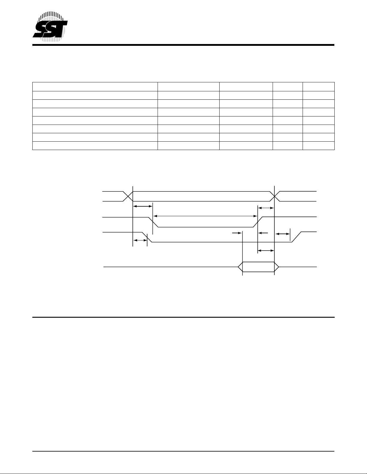
TABLE 2-6: I/O READ TIMING
Item Symbol IEEE Symbol Min Max
Data Setup before IORD# tsu(IORD) tDVIRH 20 Data Hold following IORD# th(IORD) tlGHQX 5 IORD# Width Time tw(IORD) tlGLIGH 70 Address Setup before IORD# tsuA(IORD) tAVIGL 25 Address Hold following IORD# thA(IORD) tlGHAX 10 IOCS16# Delay Falling from Address tdfIOCS16(ADR) tAVISL - 20
IOCS16# Delay Rising from Address tdrIOCS16(ADR) tAVISH - 20
Note: All times are in nanoseconds. The maximum load on IOCS16# is 1 LSTTL with 50pF total load.
All AC specifications are guaranteed by design.
T2-6.4 391
Valid Address
1
IORD#
IOCS16#
tdfIOCS16(ADR)
D15-D0
1. Valid Address consists of signals CS1FX#, CS3FX# and A2-A0.
FIGURE 2-2: I/O READ TIMING DIAGRAM
tsuA(IORD)
tw(IORD)
tsu (IORD)
thA(IORD)
tdrIOCS16(ADR)
th(IORD)
Dout
391 ILL2-7.1
©2001 Silicon Storage Technology, Inc. S71167-05-000 9/01 391
12
 Loading...