

Silicon Storage Technology Inc SST58SM192-70-C-FSJ, SST58LM048-70-C-FSJ, SST58LM048-70-C-FSI, SST58LM048-70-C-FRJ, SST58LM048-70-C-FRI Datasheet
...
©2001 Silicon Storage Technology, Inc.
S71193-01-000 9/01 519
1
The SST logo and SuperFlash are registered trademarks of Silicon Storage Technology, Inc.
These specifications are subject to change without notice.
Advance Information
FEATURES:
• ATA/IDE standard interface
– 512 Bytes per sector
– ATA command set compatible
– Selectable Master/Slave Operation
– Support Data Transfer Speed up to PIO Mode-4
• 8, 16, 24, 32, 48, 64, 96, 128, and 192 MByte
capacities
• Standard Female IDE Connector
– 40-pin and 44-pin
• Single Voltage Read and Write Operation
– 5.0V-only for SST58SMxxx
– 3.3V-only for SST58LMxxx
• Supports 5.0-Volt or 3.3-Volt Read and Write
– 4.5-5.5V or 3.135-3.465V for Commercial
• Low Power Consumption
– Active mode: 35 mA/55 mA (3.3V/5.0V) (typical)
– Sleep mode: 100 µA/150 µA (3.3V/5.0V) (typical)
• Sustained Write Performance
– Up to 1.4 MB/sec (host to flash)
• Extended Data Protection and Security
– WP# pin for Data Protection
– Factory-Programmed, 20-Byte Unique ID number
• Controller Overhead Command to DRQ
– Less than 0.5 ms
• Zero Power Data Retention
– Batteries not required for data storage
•Start Up Time
– Sleep to read: 200 ns (typical)
– Sleep to write: 200 ns (typical)
– Power-on to Ready:200 ms (typical)
• Support for Commercial Temperature Range
– 0°C to +70°C for Operating Commercial
– -50°C to +100°C for non-Operating (storage)
• Extremely Rugged and Reliable
– Built-in ECC support corrects 3 Bytes of error
per 512 Byte sector
• Intelligent ATA/IDE Controller
– Built-in microcontroller with intelligent firmware
– Built-in Embedded Flash File System
• Power Management Unit
– Immediate disabling of unused circuitry
PRODUCT DESCRIPTION
SST’s ATA-Disk Module (ADM) is a low cost, high performance, embedded flash memory data storage system.
This product is well suited for solid state mass storage
applications of fering new and expanded f uncti onal ity while
enabling cost effective designs.
The ADM is a solid state disk drive that is designed to
replace conventional IDE hard disk drive and can be
plugged into a standard IDE connector commonly found in
desktop or portable PC syst ems .
ADM has built-in microcontroller and file management
firmware that communicates with ATA standard interfaces; therefore, the ADM does not require additional or
proprietary host software such as Flash File System
(FFS) and Memory Technology Driv er (M TD) so ft w are.
The ADM is designed to work at either 5V or 3.3V and is
avai lable in 8 to 192 MByte capacit ies. It us es standard AT A
driver that is pa rt of all m aj or O S su ch a s W in dows 95/98/
2000/NT/CE, MAC, UNIX, etc.
All signals, except WP #, are in compliance with the ATA
specifications. WP# is used to write protect the information
stored on the ADM . The WP# could be c onnected to the
motherboard wri te protect control logi c through a jumper.
When WP# is low, the ADM is wr ite protected to prohibit
any inadv ertent writes.
Every ADM comes with factory-programmed, 20-Byte long,
unique identificat ion number for extended data protection .
This feature prevents unauthorized duplic ation by allowin g
encryption of customer data.
The ADM integrates a standard 40- or 44-pin female
connector for easy and co st effective mounting on top
of a standard IDE male con nector co mmonly found on
the system motherboards. ADM also offers user
selectable Master/Slave operation thro ugh an external
jumper setting.
ATA-Disk Module
SST58SM008 / 016 / 024 / 032 / 048 / 064 / 096 / 128 / 192
SST58LM008 / 016 / 024 / 032 / 048 / 064 / 096 / 128 / 192
SST58SM/LMxxxATA-Disk Module
8MB / 16MB / 24MB / 32MB / 48MB / 64MB / 96MB / 128MB / 192MB

2
Advance Information
ATA-Disk Module
SST58SM008 / 016 / 024 / 032 / 048 / 064 / 096 / 128 / 192
SST58LM008 / 016 / 024 / 032 / 048 / 064 / 096 / 128 / 192
©2001 Silicon Storage Technology, Inc. S71193-01-000 9/01 519
TABLE OF CONTENTS
PRODUCT DESCRIPTION . . . . . . . . . . . . . . . . . . . . . . . . . . . . . . . . . . . . . . . . . . . . . . . . . . . . . . . . . . . . . . . . . . . 1
1.0 GENERAL DESCRIPTION . . . . . . . . . . . . . . . . . . . . . . . . . . . . . . . . . . . . . . . . . . . . . . . . . . . . . . . . . . . . . . . 5
1.1 Performance-optimized ATA Controller . . . . . . . . . . . . . . . . . . . . . . . . . . . . . . . . . . . . . . . . . . . . . . . . . . 5
1.1.1 Microcontroller Unit (MCU). . . . . . . . . . . . . . . . . . . . . . . . . . . . . . . . . . . . . . . . . . . . . . . . . . . . . . . 5
1.1.2 Internal Direct Memory Access (DMA). . . . . . . . . . . . . . . . . . . . . . . . . . . . . . . . . . . . . . . . . . . . . . 5
1.1.3 Power Management Unit (PMU) . . . . . . . . . . . . . . . . . . . . . . . . . . . . . . . . . . . . . . . . . . . . . . . . . . 5
1.1.4 SRAM Buffer . . . . . . . . . . . . . . . . . . . . . . . . . . . . . . . . . . . . . . . . . . . . . . . . . . . . . . . . . . . . . . . . . 5
1.1.5 Embedded Flash File System . . . . . . . . . . . . . . . . . . . . . . . . . . . . . . . . . . . . . . . . . . . . . . . . . . . . 5
1.1.6 Error Correction . . . . . . . . . . . . . . . . . . . . . . . . . . . . . . . . . . . . . . . . . . . . . . . . . . . . . . . . . . . . . . . 5
1.2 SST’s ATA-Disk Module Product Offering . . . . . . . . . . . . . . . . . . . . . . . . . . . . . . . . . . . . . . . . . . . . . . . . 6
2.0 ELECTRICAL INTERFACE . . . . . . . . . . . . . . . . . . . . . . . . . . . . . . . . . . . . . . . . . . . . . . . . . . . . . . . . . . . . . . 6
2.0.1 Pin Assignment and Pin Type . . . . . . . . . . . . . . . . . . . . . . . . . . . . . . . . . . . . . . . . . . . . . . . . . . . . 6
2.1 Electrical Description . . . . . . . . . . . . . . . . . . . . . . . . . . . . . . . . . . . . . . . . . . . . . . . . . . . . . . . . . . . . . . . . 6
2.2 Absolute Maximum Stress Ratings . . . . . . . . . . . . . . . . . . . . . . . . . . . . . . . . . . . . . . . . . . . . . . . . . . . . . 9
2.3 Electrical Specification . . . . . . . . . . . . . . . . . . . . . . . . . . . . . . . . . . . . . . . . . . . . . . . . . . . . . . . . . . . . . . 10
2.3.1 Absolute Maximum Conditions. . . . . . . . . . . . . . . . . . . . . . . . . . . . . . . . . . . . . . . . . . . . . . . . . . . 10
2.3.2 Input Leakage Current . . . . . . . . . . . . . . . . . . . . . . . . . . . . . . . . . . . . . . . . . . . . . . . . . . . . . . . . . 10
2.3.3 Input Characteristics. . . . . . . . . . . . . . . . . . . . . . . . . . . . . . . . . . . . . . . . . . . . . . . . . . . . . . . . . . . 11
2.3.4 Output Drive Type . . . . . . . . . . . . . . . . . . . . . . . . . . . . . . . . . . . . . . . . . . . . . . . . . . . . . . . . . . . . 11
2.3.5 Output Drive Characteristics . . . . . . . . . . . . . . . . . . . . . . . . . . . . . . . . . . . . . . . . . . . . . . . . . . . . 11
2.3.6 I/O Input (Read) Timing Specification . . . . . . . . . . . . . . . . . . . . . . . . . . . . . . . . . . . . . . . . . . . . . 12
2.3.7 I/O Output (Write) Timing Specification . . . . . . . . . . . . . . . . . . . . . . . . . . . . . . . . . . . . . . . . . . . . 13
2.4 I/O Transfer Function. . . . . . . . . . . . . . . . . . . . . . . . . . . . . . . . . . . . . . . . . . . . . . . . . . . . . . . . . . . . . . . 14
2.4.1 I/O Function . . . . . . . . . . . . . . . . . . . . . . . . . . . . . . . . . . . . . . . . . . . . . . . . . . . . . . . . . . . . . . . . . 14
3.0 SOFTWARE INTERFACE . . . . . . . . . . . . . . . . . . . . . . . . . . . . . . . . . . . . . . . . . . . . . . . . . . . . . . . . . . . . . . 15
3.1 ATA-Disk Module Drive Register Set Definitions and Protocol . . . . . . . . . . . . . . . . . . . . . . . . . . . . . . . 15
3.1.1 ATA-Disk Module Addressing . . . . . . . . . . . . . . . . . . . . . . . . . . . . . . . . . . . . . . . . . . . . . . . . . . . 15
3.1.2 ATA-Disk Module Registers . . . . . . . . . . . . . . . . . . . . . . . . . . . . . . . . . . . . . . . . . . . . . . . . . . . . . 15
3.1.2.1 Data Register . . . . . . . . . . . . . . . . . . . . . . . . . . . . . . . . . . . . . . . . . . . . . . . . . . . . . . . . . 15
3.1.2.2 Error Register (Read Only) . . . . . . . . . . . . . . . . . . . . . . . . . . . . . . . . . . . . . . . . . . . . . . . 15
3.1.2.3 Feature Register (Write Only) . . . . . . . . . . . . . . . . . . . . . . . . . . . . . . . . . . . . . . . . . . . . . 16
3.1.2.4 Sector Count Register. . . . . . . . . . . . . . . . . . . . . . . . . . . . . . . . . . . . . . . . . . . . . . . . . . . 16
3.1.2.5 Sector Number (LBA 7-0) Register . . . . . . . . . . . . . . . . . . . . . . . . . . . . . . . . . . . . . . . . . 16
3.1.2.6 Cylinder Low (LBA 15-8) Register. . . . . . . . . . . . . . . . . . . . . . . . . . . . . . . . . . . . . . . . . . 16
3.1.2.7 Cylinder High (LBA 23-16) Register . . . . . . . . . . . . . . . . . . . . . . . . . . . . . . . . . . . . . . . . 16
3.1.2.8 Drive/Head (LBA 27-24) Register . . . . . . . . . . . . . . . . . . . . . . . . . . . . . . . . . . . . . . . . . . 16
3.1.2.9 Status & Alternate Status Registers (Read Only) . . . . . . . . . . . . . . . . . . . . . . . . . . . . . . 17
3.1.2.10 Device Control Register (Write Only) . . . . . . . . . . . . . . . . . . . . . . . . . . . . . . . . . . . . . . 17
3.1.2.11 Drive Address Register (Read Only). . . . . . . . . . . . . . . . . . . . . . . . . . . . . . . . . . . . . . . 18
3.1.2.12 Command Register (Write Only) . . . . . . . . . . . . . . . . . . . . . . . . . . . . . . . . . . . . . . . . . . 18

Advance Information
ATA-Disk Module
SST58SM008 / 016 / 024 / 032 / 048 / 064 / 096 / 128 / 192
SST58LM008 / 016 / 024 / 032 / 048 / 064 / 096 / 128 / 192
3
©2001 Silicon Storage Technology, Inc. S71193-01-000 9/01 519
3.2 ATA-Disk Module Command Description. . . . . . . . . . . . . . . . . . . . . . . . . . . . . . . . . . . . . . . . . . . . . . . . 19
3.2.1 ATA-Disk Module Command Set . . . . . . . . . . . . . . . . . . . . . . . . . . . . . . . . . . . . . . . . . . . . . . . . . 19
3.2.1.1 Check Power Mode - 98H or E5H. . . . . . . . . . . . . . . . . . . . . . . . . . . . . . . . . . . . . . . . . . 20
3.2.1.2 Execute Drive Diagnostic - 90H . . . . . . . . . . . . . . . . . . . . . . . . . . . . . . . . . . . . . . . . . . . 20
3.2.1.3 Format Track - 50H. . . . . . . . . . . . . . . . . . . . . . . . . . . . . . . . . . . . . . . . . . . . . . . . . . . . . 21
3.2.1.4 Identify Drive - ECH. . . . . . . . . . . . . . . . . . . . . . . . . . . . . . . . . . . . . . . . . . . . . . . . . . . . . 21
3.2.1.4.1 General Configuration. . . . . . . . . . . . . . . . . . . . . . . . . . . . . . . . . . . . . . . . . . . . 23
3.2.1.4.2 Default Number of Cylinders. . . . . . . . . . . . . . . . . . . . . . . . . . . . . . . . . . . . . . . 23
3.2.1.4.3 Default Number of Heads. . . . . . . . . . . . . . . . . . . . . . . . . . . . . . . . . . . . . . . . . 23
3.2.1.4.4 Default Number of Sectors per Track . . . . . . . . . . . . . . . . . . . . . . . . . . . . . . . . 23
3.2.1.4.5 Number of Sectors . . . . . . . . . . . . . . . . . . . . . . . . . . . . . . . . . . . . . . . . . . . . . . 23
3.2.1.4.6 Memory Serial Number. . . . . . . . . . . . . . . . . . . . . . . . . . . . . . . . . . . . . . . . . . . 23
3.2.1.4.7 Buffer Type. . . . . . . . . . . . . . . . . . . . . . . . . . . . . . . . . . . . . . . . . . . . . . . . . . . . 23
3.2.1.4.8 Buffer Size . . . . . . . . . . . . . . . . . . . . . . . . . . . . . . . . . . . . . . . . . . . . . . . . . . . . 23
3.2.1.4.9 ECC Count . . . . . . . . . . . . . . . . . . . . . . . . . . . . . . . . . . . . . . . . . . . . . . . . . . . . 23
3.2.1.4.10 Firmware Revision . . . . . . . . . . . . . . . . . . . . . . . . . . . . . . . . . . . . . . . . . . . . . 23
3.2.1.4.11 Model Number . . . . . . . . . . . . . . . . . . . . . . . . . . . . . . . . . . . . . . . . . . . . . . . . 23
3.2.1.4.12 Read/Write Multiple Sector Count . . . . . . . . . . . . . . . . . . . . . . . . . . . . . . . . . 23
3.2.1.4.13 Capabilities. . . . . . . . . . . . . . . . . . . . . . . . . . . . . . . . . . . . . . . . . . . . . . . . . . . 23
3.2.1.4.14 PIO Data Transfer Cycle Timing Mode. . . . . . . . . . . . . . . . . . . . . . . . . . . . . . 23
3.2.1.4.15 Translation Parameters Valid . . . . . . . . . . . . . . . . . . . . . . . . . . . . . . . . . . . . . 24
3.2.1.4.16 Current Number of Cylinders, Heads, Sectors/Track . . . . . . . . . . . . . . . . . . . 24
3.2.1.4.17 Current Capacity. . . . . . . . . . . . . . . . . . . . . . . . . . . . . . . . . . . . . . . . . . . . . . . 24
3.2.1.4.18 Multiple Sector Setting . . . . . . . . . . . . . . . . . . . . . . . . . . . . . . . . . . . . . . . . . . 24
3.2.1.4.19 Total Sectors Addressable in LBA Mode . . . . . . . . . . . . . . . . . . . . . . . . . . . . 24
3.2.1.4.20 Advanced PIO Data Transfer Mode . . . . . . . . . . . . . . . . . . . . . . . . . . . . . . . . 24
3.2.1.4.21 Minimum PIO Transfer Cycle Time Without Flow Control . . . . . . . . . . . . . . . 24
3.2.1.4.22 Minimum PIO Transfer Cycle Time with IORDY. . . . . . . . . . . . . . . . . . . . . . . 24
3.2.1.5 Idle - 97H or E3H. . . . . . . . . . . . . . . . . . . . . . . . . . . . . . . . . . . . . . . . . . . . . . . . . . . . . . . 25
3.2.1.6 Idle Immediate - 95H or E1H. . . . . . . . . . . . . . . . . . . . . . . . . . . . . . . . . . . . . . . . . . . . . . 25
3.2.1.7 Initialize Drive Parameters - 91H. . . . . . . . . . . . . . . . . . . . . . . . . . . . . . . . . . . . . . . . . . . 25
3.2.1.8 Read Buffer - E4H. . . . . . . . . . . . . . . . . . . . . . . . . . . . . . . . . . . . . . . . . . . . . . . . . . . . . . 26
3.2.1.9 Read Multiple - C4H . . . . . . . . . . . . . . . . . . . . . . . . . . . . . . . . . . . . . . . . . . . . . . . . . . . . 26
3.2.1.10 Read Long Sector - 22H or 23H . . . . . . . . . . . . . . . . . . . . . . . . . . . . . . . . . . . . . . . . . . 27
3.2.1.11 Read Sectors - 20H or 21H. . . . . . . . . . . . . . . . . . . . . . . . . . . . . . . . . . . . . . . . . . . . . . 27
3.2.1.12 Read Verify Sector(s) - 40H or 41H . . . . . . . . . . . . . . . . . . . . . . . . . . . . . . . . . . . . . . . 28
3.2.1.13 Recalibrate - 1XH . . . . . . . . . . . . . . . . . . . . . . . . . . . . . . . . . . . . . . . . . . . . . . . . . . . . . 28
3.2.1.14 Seek - 7XH . . . . . . . . . . . . . . . . . . . . . . . . . . . . . . . . . . . . . . . . . . . . . . . . . . . . . . . . . . 28
3.2.1.15 Set Features - EFH . . . . . . . . . . . . . . . . . . . . . . . . . . . . . . . . . . . . . . . . . . . . . . . . . . . . 29
3.2.1.16 Set Multiple Mode - C6H . . . . . . . . . . . . . . . . . . . . . . . . . . . . . . . . . . . . . . . . . . . . . . . . 30
3.2.1.17 Set Sleep Mode - 99H or E6H. . . . . . . . . . . . . . . . . . . . . . . . . . . . . . . . . . . . . . . . . . . . 30
3.2.1.18 Standby - 96H or E2H. . . . . . . . . . . . . . . . . . . . . . . . . . . . . . . . . . . . . . . . . . . . . . . . . . 31
3.2.1.19 Standby Immediate - 94H or E0H . . . . . . . . . . . . . . . . . . . . . . . . . . . . . . . . . . . . . . . . . 31
3.2.1.20 Write Buffer - E8H. . . . . . . . . . . . . . . . . . . . . . . . . . . . . . . . . . . . . . . . . . . . . . . . . . . . . 31
3.2.1.21 Write Long Sector - 32H or 33H . . . . . . . . . . . . . . . . . . . . . . . . . . . . . . . . . . . . . . . . . . 32
3.2.1.22 Write Multiple Command - C5H. . . . . . . . . . . . . . . . . . . . . . . . . . . . . . . . . . . . . . . . . . . 32
3.2.1.23 Write Sector(s) - 30H or 31H. . . . . . . . . . . . . . . . . . . . . . . . . . . . . . . . . . . . . . . . . . . . . 33
3.2.1.24 Write Verify - 3CH . . . . . . . . . . . . . . . . . . . . . . . . . . . . . . . . . . . . . . . . . . . . . . . . . . . . . 33
3.2.2 Error Posting . . . . . . . . . . . . . . . . . . . . . . . . . . . . . . . . . . . . . . . . . . . . . . . . . . . . . . . . . . . . . . . . 34

4
Advance Information
ATA-Disk Module
SST58SM008 / 016 / 024 / 032 / 048 / 064 / 096 / 128 / 192
SST58LM008 / 016 / 024 / 032 / 048 / 064 / 096 / 128 / 192
©2001 Silicon Storage Technology, Inc. S71193-01-000 9/01 519
4.0 APPENDIX . . . . . . . . . . . . . . . . . . . . . . . . . . . . . . . . . . . . . . . . . . . . . . . . . . . . . . . . . . . . . . . . . . . . . . . . . . 35
4.1 Differences between ATA-Disk Module and ATA/ATAPI-5 Specifications. . . . . . . . . . . . . . . . . . . . . . . 35
4.1.1 Electrical Differences . . . . . . . . . . . . . . . . . . . . . . . . . . . . . . . . . . . . . . . . . . . . . . . . . . . . . . . . . . 35
4.1.1.1 TTL Compatibility . . . . . . . . . . . . . . . . . . . . . . . . . . . . . . . . . . . . . . . . . . . . . . . . . . . . . . 35
4.1.1.2 Pull Up Resistor Input Leakage Current . . . . . . . . . . . . . . . . . . . . . . . . . . . . . . . . . . . . . 35
4.1.2 Functional Differences . . . . . . . . . . . . . . . . . . . . . . . . . . . . . . . . . . . . . . . . . . . . . . . . . . . . . . . . . 35
4.1.2.1 Idle Timer . . . . . . . . . . . . . . . . . . . . . . . . . . . . . . . . . . . . . . . . . . . . . . . . . . . . . . . . . . . . 35
4.1.2.2 Recovery from Sleep Mode. . . . . . . . . . . . . . . . . . . . . . . . . . . . . . . . . . . . . . . . . . . . . . . 35
5.0 PHYSICAL DIMENSIONS . . . . . . . . . . . . . . . . . . . . . . . . . . . . . . . . . . . . . . . . . . . . . . . . . . . . . . . . . . . . . . 36
6.0 PRODUCT ORDERING INFORMATION . . . . . . . . . . . . . . . . . . . . . . . . . . . . . . . . . . . . . . . . . . . . . . . . . . . 38
6.1 Valid Combinations . . . . . . . . . . . . . . . . . . . . . . . . . . . . . . . . . . . . . . . . . . . . . . . . . . . . . . . . . . . . . . . . 38
7.0 LIMITED WARRANTY . . . . . . . . . . . . . . . . . . . . . . . . . . . . . . . . . . . . . . . . . . . . . . . . . . . . . . . . . . . . . . . . . 40
7.1 Life Support Policy. . . . . . . . . . . . . . . . . . . . . . . . . . . . . . . . . . . . . . . . . . . . . . . . . . . . . . . . . . . . . . . . . 40
7.2 Patent Protection . . . . . . . . . . . . . . . . . . . . . . . . . . . . . . . . . . . . . . . . . . . . . . . . . . . . . . . . . . . . . . . . . . 40
Advance Information
ATA-Disk Module
SST58SM008 / 016 / 024 / 032 / 048 / 064 / 096 / 128 / 192
SST58LM008 / 016 / 024 / 032 / 048 / 064 / 096 / 128 / 192
5
©2001 Silicon Storage Technology, Inc. S71193-01-000 9/01 519
1.0 GENERAL DESCRIPTION
The SST’s ATA-Disk Module (ADM) contains a controller,
embedded firmware, and Flash Media with a 40-pin or 44pin female connector. Refer to Figure 1-1 for SST’s ADM
block diagram. The controller interfaces with th e host system allowing data to b e w ritten to and rea d f ro m the Fla s h
Media.
1.1 Perf ormance-optimized AT A Contr oller
The heart of the ADM is the A TA controller which translates
standard ATA signals into Flash Media d ata and contro ls.
SST’s ADM contains a p roprietary ATA controller sp ecifically designed to attain high d ata throughpu t from host t o
Flash. The following components contribute to the A T A controller’s performance.
1.1.1 Microcontroller Unit (MCU)
The MCU translates ATA co mmands in to data an d control
signals required for flash memory operation.
1.1.2 Internal Direct Memory Access (DMA)
The ATA controller inside ADM uses DMA allowing i nstan t
data transfer from buffer to memory. This implementation
eliminates microc ontroller overhead associated with traditional, firmware based, memory control, increasing data
transfer rate.
1.1.3 Power Management Unit (PMU)
Power Management Unit controls the power c onsumptio n
of the ADM. The PMU dramatically extends product battery
life by putting the part of the circuitry that is not in operation
into sleep mode.
1.1.4 SRAM Buffer
A key contributor to the ATA contro ller performance is an
SRAM buffer. The buffer optimizes the data writes to Flash.
1.1.5 Embedded Flash File System
Embedded Flash File System is an integral part of the
SST’s ATM controll er. It contains MCU Fir mware that performs the f ollow ing tasks:
1. Translates host side signals into Flash Media
Writes and Reads.
2. Provides Flash Media wear leveling to spread the
Flash writes across all the memory address space
to increase the longevity of Flash Media.
3. Keeps track of data file structures.
1.1.6 Error Correction
The ATA Controller contains ECC algorithm that corrects 3
bytes of error per 512 Byte sector.
FIGURE 1-1: SST ATA-D
ISK MODULE BLOCK DIAGRAM
519 ILL1-1.4
40 or 44-Pin
Male IDE Connector
40 or 44-Pin
Female IDE Connector
PC
Mother
Board
ATA Controller
Flash
Media
Embedded
Flash
File System
MCU
ECC
Internal
DMA
SRAM Buffer
PMU
ATA-Disk Module
6
Advance Information
ATA-Disk Module
SST58SM008 / 016 / 024 / 032 / 048 / 064 / 096 / 128 / 192
SST58LM008 / 016 / 024 / 032 / 048 / 064 / 096 / 128 / 192
©2001 Silicon Storage Technology, Inc. S71193-01-000 9/01 519
1.2 SST’s ATA-Disk Module Product Offering
The SST58SM/LMxx x ATA-Disk Module produc t family is available in 8 to 192 MB yte den si tie s. The following table
shows the specific capacity, default number of cylinder heads, sectors and cylinders for each product line.
2.0 ELECTRICAL INTERFACE
2.0.1 Pin Assignment and Pin Type
The signal/pin assignme nts are listed in Tables 2- 1 and 2-2. Low active signals have a “#” suffix. Pin types are
Input, Output or Input/Output. Section 2.3 defines the DC characteristics for all input and output type structures.
2.1 Electrical Description
The ADM functions in ATA Mode, which is compatible with IDE hard disk drives.
Table 2-3 describe s the I/O si gnals. Signals whose sourc e is the h ost are desi gnated as i nputs while s ignals that
the ADM sources are outputs. All outputs from the ADM are totem pole except the data bus signals which are in the
bi-directional tri-state. Refer to Section 2.3.2 for definitions of Input and Output types.
Model Number Density T ota l Bytes Cylinders Heads Sectors
SST58SM/LM008 8 MB 8,028,160 245 2 32
SST58SM/LM016 16 MB 16,023,552 489 2 32
SST58SM/LM024 24 MB 24,051,712 367 4 32
SST58SM/LM032 32 MB 32,047,104 489 4 32
SST58SM/LM048 48 MB 48,037,888 733 4 32
SST58SM/LM064 64 MB 64,028,672 977 4 32
SST58SM/LM096 96 MB 96,075,776 733 8 32
SST58SM/LM128 128 MB 128,057 ,344 977 8 32
SST58SM/LM192 192 MB 192,151 ,552 733 16 32
Advance Information
ATA-Disk Module
SST58SM008 / 016 / 024 / 032 / 048 / 064 / 096 / 128 / 192
SST58LM008 / 016 / 024 / 032 / 048 / 064 / 096 / 128 / 192
7
©2001 Silicon Storage Technology, Inc. S71193-01-000 9/01 519
TABLE 2-1: 44-PIN PIN ASSIGNMENT
Pin No. Signal Name Pin Type I/O Type
1
1 RESET# I I4U
2 GND Ground
3 D7 I/O I2D, O2
4 D8 I/O I2D, O2
5 D6 I/O I2D, O2
6 D9 I/O I2D, O2
7 D5 I/O I2D, O2
8 D10 I/O I2D, O2
9 D4 I/O I2D, O2
10 D11 I/O I2D, O2
11 D3 I/O I2D, O2
12 D12 I/O I2D, O2
13 D2 I/O I2D, O2
14 D13 I/O I2D, O2
15 D1 I/O I2D, O2
16 D14 I/O I2D, O2
17 D0 I/O I2D, O2
18 D15 I/O I2D, O2
19 GND Ground
20 NC
21 NC
22 GND Ground
23 IOWR# I I3U
24 GND Ground
25 IORD# I I3U
26 GND Ground
27 NC
28 NC
2
29 NC
30 NC/WP#
3
I2U
31 INTRQ O O1
32 IOCS16# O O2
33 A1 I I2D
34 PDIAG# I/O I2U, O1
35 A0 I I2D
36 A2 I I2D
37 CS1FX# I I3U
38 CS3FX# I I3U
39 DASP# I/O I2U, O1
40 GND Ground
41 V
DD
Power
42 V
DD
Power
43 GND Ground
44 NC
T2-1.6 519
1. Please refer to Sections 2.3.1 to 2.3.4 for detail
2. Pin 28 is CSEL in standard host 40- pin IDE int erf ace. Master /
Slave setting i s selected t hrough an on-bo ard jumper.
3. Pin 30 is jumper selectable as NC or WP#.
TABLE 2-2: 40-PIN PIN ASSIGNMENT
Pin No. Signal Name Pin Type I/O Type
1
1 RESET# I I4U
2 GND Ground
3 D7 I/O I2D, O2
4 D8 I/O I2D, O2
5 D6 I/O I2D, O2
6 D9 I/O I2D, O2
7 D5 I/O I2D, O2
8 D10 I/O I2D, O2
9 D4 I/O I2D, O2
10 D11 I/O I2D, O2
11 D3 I/O I2D, O2
12 D12 I/O I2D, O2
13 D2 I/O I2D, O2
14 D13 I/O I2D, O2
15 D1 I/O I2D, O2
16 D14 I/O I2D, O2
17 D0 I/O I2D, O2
18 D15 I/O I2D, O2
19 GND Ground
20 V
DD
2
Power
21 NC
22 GND Ground
23 IOWR# I I3U
24 GND Ground
25 IORD# I I3U
26 GND Ground
27 NC
28 NC
3
29 NC
30 NC/WP#
4
I2U
31 INTRQ O O1
32 IOCS16# O O2
33 A1 I I2D
34 PDIAG# I/O I2U, O1
35 A0 I I2D
36 A2 I I2D
37 CS1FX# I I3U
38 CS3FX# I I3U
39 DASP# I/O I2U, O1
40 GND Ground
T2-2.6 519
1. Please refer to Sections 2.3.1 to 2.3.4 for detail.
2. Optional, not av ai lab le in sta ndard host 40 -pin IDE interf a ce.
3. Pin 28 is CSEL in standard host 40- pin IDE int erf ace. Master /
Slave setting i s selected t hrough an on-bo ard jumper.
4. Pin 30 is jumper selectable as NC or WP#.
8
Advance Information
ATA-Disk Module
SST58SM008 / 016 / 024 / 032 / 048 / 064 / 096 / 128 / 192
SST58LM008 / 016 / 024 / 032 / 048 / 064 / 096 / 128 / 192
©2001 Silicon Storage Technology, Inc. S71193-01-000 9/01 519
For the 40-pin ATA-Disk Module, power can be supplied either through the pin 20 (not presen t on standard 40- pin
IDE interface) or through the external power connector provided on the 40- pin ADM. Please see the drawings in
“Physical Dimensions” on page 36 for information.
FIGURE 2-1: P
IN 30 CONFIGURATION
TABLE 2-3: SIGNAL DESCRIPTION
Symbol Type1Pin Name and Functions
A2 - A0 I 33,34,35 A[2:0] are used to select one of the Task File registers.
D15 - D0 I/O 18,16,14,12,10,
8,6,4,3,5,7,9,11,
13,15,17
Data bus
CS1FX#, CS3FX# I 37,38 CS1FX# is the chip select for the task file registers while CS3FX# is used to
select the Alternate Status Register and the Device Control Register.
CSEL - 28 CSEL signal is a NC to the motherboard. The Master/Slave selection is set by a
jumper. If the jumper is in a Master position, the ADM is addressed as a Master
drive, and if the jumper is in a Slave position, the ADM is addressed as a Slave
drive.
IORD# I 25 This is an I/O Read st robe gener ated b y the host. This signa l gates I/O data
onto the bus from the chip.
IOWR# I 23 The I/O Write strobe pulse is used to clock I/O data into the chip.
IOCS16# O 32 This output signal is asserted low when this dev ice is e xp ecting a w ord data
transfer cy cl e .
INTRQ O 31 Signal is the active high Interrupt Request to the host.
PDIAG# I/O 34 This input/output is the Pass Diagnostic signal in the Master/Slave hand-
shake protocol.
DASP# I/O 39 This inp ut/output is the Disk Activ e/Sla v e present sign al in the Maste r/Slav e
handshake prot oco l.
RESET# I 1 This input pin is the active low hardware reset from the host.
GND - 2,19,22,24,26,
30,40,43
2
Ground
WP#
3
I 30 Write protect pin is used to disable Write operation. The 3-position jumper can set
pin 30 as NC, write protected (by connecting to GND), or host selectable (by connecting to pin 30 of IDE connector). When the signal on this pin is low , data on the
chip will be write-protected. (See Figure 2-1)
V
DD
-204, 412, 42
2
Power
T2-3.6 519
1. Please refer to Sections 2.3.1 to 2.3.4 for detail
2. Only available with the 44-pin connector module
3. Pin 30 is jumper selectable as NC or WP#
4. Only available with the 40-pin connector module
519 ILL2-5.1
ATA Controller
Flash
Memory
231
Pin 30
WP# Jumper
ATA-Disk Module
WP# Jumper A TA-Disk Module
No Jumper NC, Module is NOT write protected.
Close 1, 2 Connect to Ground,
Module is write protected
Close 2, 3 Host Selectable,
Module is write protected if pin 30 is low.
Module is NOT write protected if pin 30
is high.
T2-3.0 519

Advance Information
ATA-Disk Module
SST58SM008 / 016 / 024 / 032 / 048 / 064 / 096 / 128 / 192
SST58LM008 / 016 / 024 / 032 / 048 / 064 / 096 / 128 / 192
9
©2001 Silicon Storage Technology, Inc. S71193-01-000 9/01 519
2.2 Absolute Maximum Stress Ratings
Absolute Maximum Stress Ratings (Applied conditions greater than those listed under “Absolute Maximum
Stress Ratings” may cause pe r manent dama ge to the device. This i s a stress rating only an d funct ional operatio n
of the device at these conditions or conditions greater tha n those defined in the ope rational sections of this data
sheet is not implied. Exposure to absolute maximum stress rating conditions may affect device reliability.)
Temperature Under Bias . . . . . . . . . . . . . . . . . . . . . . . . . . . . . . . . . . . . . . . . . . . . . . . . . . . . . . . . . -55°C to +125°C
Storage Temperature . . . . . . . . . . . . . . . . . . . . . . . . . . . . . . . . . . . . . . . . . . . . . . . . . . . . . . . . . . . . -50°C to +100°C
D.C. Voltage on any Pin to Ground Potential . . . . . . . . . . . . . . . . . . . . . . . . . . . . . . . . . . . . . . . . .-0.5V to V
DD
+0.5V
Transient Voltage (<20 ns) on Any Pin to Ground Potential. . . . . . . . . . . . . . . . . . . . . . . . . . . . . .-1.0V to V
DD
+1.0V
Package Power Dissipation Capability (Ta = 25°C) . . . . . . . . . . . . . . . . . . . . . . . . . . . . . . . . . . . . . . . . . . . . . . 1.0W
Through Hole Lead Soldering Temperature (10 Seconds). . . . . . . . . . . . . . . . . . . . . . . . . . . . . . . . . . . . . . . . 300° C
Surface Mount Lead Soldering Temperature (3 Seconds). . . . . . . . . . . . . . . . . . . . . . . . . . . . . . . . . . . . . . . . 240° C
Output Short Circ uit Curr ent
1
. . . . . . . . . . . . . . . . . . . . . . . . . . . . . . . . . . . . . . . . . . . . . . . . . . . . . . . . . . . . . 50 mA
1. Outputs shorted for no more than one second. No more than one output shorted at a time.
OPERATING RANGE: SST58SMXXX
Range Ambient Temp V
DD
Commercia l 0°C to +70°C 4.5-5.5V
OPERATING RANGE: SST58LMXXX
Range Ambient Temp V
DD
Commercial 0°C to +70°C 3.135-3.465V
AC CONDITIONS OF TEST
Input Rise/Fall Time . . . . . . . . . . . . . . 10 ns
Output Load . . . . . . . . . . . . . . . . . . . . C
L
= 100 pF
See Figure 2-3
Note: All AC specifications are guaranteed by design.
TABLE 2-4: RECOMMENDED SYSTEM POWER-UP TIMINGS
Symbol Parameter Maximum Units
T
PU-READY
1
1. This parameter is measured only for initial qualification and after a design or process change that could affect this parameter.
Power-up to Ready Operation 500 ms
T
PU-WRITE
1
Power-up to Program/Erase Operation 500 ms
T2-4.0 519
10
Advance Information
ATA-Disk Module
SST58SM008 / 016 / 024 / 032 / 048 / 064 / 096 / 128 / 192
SST58LM008 / 016 / 024 / 032 / 048 / 064 / 096 / 128 / 192
©2001 Silicon Storage Technology, Inc. S71193-01-000 9/01 519
2.3 Electrical Specification
The following tables define all D.C. Characteristics for the SST ATA-Disk Module product family.
2.3.1 Absolute Maximum Conditions
Unless otherwise stated, conditions are for Commercial Temperature:
Non-operating (storage) temperature range: -50°C to +100°C
V
DD
= 4.5-5.5V
V
DD
= 3.135-3.465V
Ta = 0°C to +70°C
ADM products shall operate correctly in both voltage ranges as shown in the tables above. To comply with th is
specification, current requirements must not exceed the maximum limit.
2.3.2 Input Leakage Current
In the table below, x refers to the characteristics descr ibed in Sectio n 2.3.2. For example, I1U indicates a pul l up
resistor with a type 1 input characteristic.
A
BSOLUTE MAXIMUM CONDITIONS
Parameter Symbol Conditions
Input Powe r V
DD
-0.3V min to 6.5V max
Voltage on any pin except V
DD
with respect to GND V -0.5V min to VDD + 0.5V max
INPUT POWER
Voltage
Maximum Average RMS
Active Current
Maximum Average RMS
Sleep Current Measurement Method
3.135-3.465V 75 mA 200 µA 3.3V at 25
°C
1
1. Current measurement is accomplished by connecting an amp meter (set to the 2 amp scale range) in series with the VDD supply to
the ADM. Current measurements are to be taken while looping on a data transfer command with a sector count of 128. Current consumption values for both Read and Write commands are not to exceed the Maximum Average RMS Current specified in the above
table.
4.5-5.5V 100 mA 300 µA 5.0V at 25°C
1
Type Parameter Symbol Conditions MIN TYP MAX Units
IxZ Input Leakage Current IL V
IH
= VDD / VIL = Gnd -1 1 µA
IxU Pull Up Resistor RPU1 VDD = 5.0V 50k 500k Ohm
IxD Pull Down Resistor RPD1 VDD = 5.0V 50k 500k Ohm
Advance Information
ATA-Disk Module
SST58SM008 / 016 / 024 / 032 / 048 / 064 / 096 / 128 / 192
SST58LM008 / 016 / 024 / 032 / 048 / 064 / 096 / 128 / 192
11
©2001 Silicon Storage Technology, Inc. S71193-01-000 9/01 519
2.3.3 Input Characteristics
2.3.4 Output Drive Type
All output drive type are CMOS level.
2.3.5 Output Drive Characteristics
Type Parameter Symbol
Min Typ Max Min Typ Max
UnitsVDD = 3.3V VDD = 5.0V
1 Input Voltage V
IH
2.4 2.4 Volts
CMOS V
IL
0.6 0.8
2 Input Voltage V
IH
2.0 2.7 Volts
CMOS V
IL
0.8 0.8
3 Input Voltage V
TH
2.0 2.4 Volts
CMOS V
TL
0.5 0.8
Schmitt Trigger
4 Input Voltage V
TH
1.8 2.4 Volts
CMOS V
TL
0.9 0.8
Schmitt Trigger
Type Parameter Symbol Conditions MIN TYP MAX Units
O1 Output Voltage V
OH
IOH = -4 mA VDD-0.8V Volts
V
OL
IOL = 4 mA Gnd+0.4V
O2 Output Voltage V
OH
IOH = -8 mA VDD-0.8V Volts
V
OL
IOL = 8 mA Gnd+0.4V
12
Advance Information
ATA-Disk Module
SST58SM008 / 016 / 024 / 032 / 048 / 064 / 096 / 128 / 192
SST58LM008 / 016 / 024 / 032 / 048 / 064 / 096 / 128 / 192
©2001 Silicon Storage Technology, Inc. S71193-01-000 9/01 519
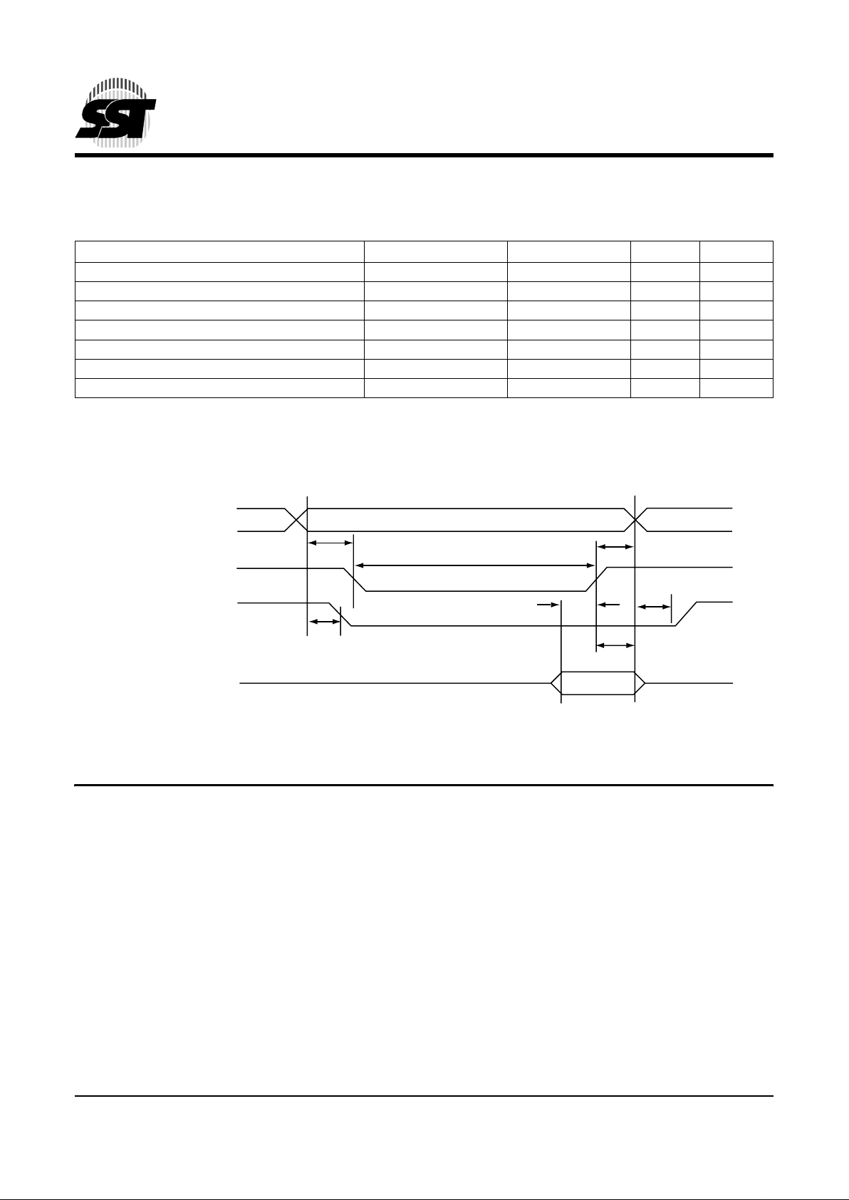
2.3.6 I/O Input (Read) Timing Specification
Note: All times are in nanoseconds. The maximum load on IOCS16# is 1 LSTTL with 50pF total load.
All AC specifications are guaranteed by design.
FIGURE 1: I/O READ TIMING DIAGRAM
TABLE 2-5: I/O READ TIMING
Item Symbol IEEE Symbol Min Max
Data Setup before IORD# tsu(IORD) tDVIRH 20 Data Hold following IORD# th(IORD) tlGHQX 5 IORD# Width Time tw(IORD) tlGLIGH 70 Valid Address Setup before IORD# tsuA(IORD) tAVIGL 25 Valid Address Hold following IORD# thA(IORD) tlGHAX 10 IOCS16# Delay Falling from Address tdfIOCS16(ADR) tAVISL - 20
IOCS16# Delay Rising from Address tdrIOCS16(ADR) tAVISH 20
T2-5.4 519
519 ILL2-7.3
tdrIOCS16(ADR)
tdfIOCS16(ADR)
thA(IORD)
th(IORD)
tsuA(IORD)
tsu (IORD)
tw(IORD)
Valid Address
1
IORD#
IOCS16#
D15-D0
Dout
1. Valid Address consists of signals CS1FX#, CS3FX#, and A2-A0.
 Loading...