

Silicon Storage Technology Inc SST49LF040-33-4C-WH Datasheet

FEATURES:
4 Mbit LPC Flash
SST49LF040
SST49LF0404 Mb LPC Flash
Advance Information
• LPC Interface Flash
– SST49LF040: 512K x8 (4 Mbit)
• Conforms to Intel LPC Interface Specification 1.0
• Flexible Erase Capability
– Uniform 4 KByte sectors
– Uniform 64 KByte overlay blocks
– 64 KByte Top boot block protection
– Chip-Erase for PP Mode Only
• Single 3.0-3.6V Read and Write Operations
• Superior Reliability
– Endurance: 100,000 Cycles (typical)
– Greater than 100 years Data Retention
• Low Power Consumption
– Active Read Current: 6 mA (typical)
– Standby Current: 10 µA (typical)
• Fast Sector-Erase/Byte-Program Operation
– Sector-Erase Time: 18 ms (typical)
– Block-Erase Time: 18 ms (typical)
– Chip-Erase Time: 70 ms (typical)
– Byte-Program Time: 14 µs (typical)
– Chip Rewrite Time: 8 seconds (typical)
– Single-pulse Program or Erase
– Internal timing generation
• Two Operational Modes
– Low Pin Count (LPC) Interface mode for
in-system operation
– Parallel Programming (PP) mode for fast production
programming
• LPC Interface Mode
– 5-signal communication interface supporting
byte Read and Write
– 33 MHz clock frequency operation
– WP# and TBL# pins provide hardware write protect
for entire chip and/or top boot block
– Standard SDP Command Set
– Data# Polling and Toggle Bit for End-of-Write
detection
– 5 GPI pins for system design flexibility
– ID pins for multi-chip selection
– Decode both top and bottom regions of the
system memory map
• Parallel Programming (PP) Mode
– 11-pin multiplexed address and 8-pin data
I/O interface
– Supports fast programming In-System on pro-
grammer equipment
• CMOS and PCI I/O Compatibility
• Packages Available
– 32-lead PLCC
– 32-lead TSOP (8mm x 14mm)
PRODUCT DESCRIPTION
The SST49LF040 flash memory devices are designed to
interface with the LPC bus for PC and Internet Appliance
application in compliance with Intel Low Pin Count (LPC)
Interface Specification 1.0. Two interface modes are supported by the SST49LF040: LPC mode for In-System
operation and Parallel Programming (PP) mode to interface
with programmer equipment.
The SST49LF040 flash memory devices are manufactured
with SST’s proprietary, high performance SuperFlash Technology. The split-gate cell design and thick oxide tunneling
injector attain better reliability and manufacturability compared with alternate approaches. The SST49LF040 device
significantly improves performance and reliability, while lowering power consumption. The SST49LF040 device writes
(Program or Erase) with a single 3.0-3.6V power supply. It
uses less energy during Erase and Program than alternative flash memory technologies. The total energy consumed is a function of the applied voltage, current and time
of application. Since for any give voltage range, the SuperFlash technology uses less current to program and has a
©2001 Silicon Stor age Technology, Inc.
S71213-00-000 11/01 562
1
shorter erase time, the total energy consumed during any
Erase or Program operation is less than alternative flash
memory technologies. The SST49LF040 product provides
a maximum Byte-Program time of 20 µsec. The entire
memory can be erased and programmed byte-by-byte typically in 8 seconds when using status detection features
such as Toggle Bit or Data# Polling to indicate the completion of Program operation. The SuperFlash technology provides fixed Erase and Program time, independent of the
number of Erase/Program cycles that have performed.
Therefore the system software or hardware does not have
to be calibrated or correlated to the cumulative number of
erase cycles as is necessary with alternative flash memory
technologies, whose Erase and Program time increase
with accumulated Erase/Program cycles.
To meet high density, surface mount requirements, the
SST49LF040 device is offered in 32-lead TSOP and 32lead PLCC packages. See Figures 2 and 3 for pin assignments and Table 1 for pin descriptions.
The SST logo and SuperFlash are registered trademarks of Silicon Storage Technology, Inc.
Intel is a registered trademark of Intel Corporation.
These specifications are subject to change without notice.

4 Mbit LPC Flash
SST49LF040
Advance Information
TABLE OF CONTENTS
PRODUCT DESCRIPTION . . . . . . . . . . . . . . . . . . . . . . . . . . . . . . . . . . . . . . . . . . . . . . . . . . . . . . . . . . . . . . . . . . . 1
LIST OF FIGURES . . . . . . . . . . . . . . . . . . . . . . . . . . . . . . . . . . . . . . . . . . . . . . . . . . . . . . . . . . . . . . . . . . . . . . . . . 4
LIST OF TABLES. . . . . . . . . . . . . . . . . . . . . . . . . . . . . . . . . . . . . . . . . . . . . . . . . . . . . . . . . . . . . . . . . . . . . . . . . . . 5
FUNCTIONAL BLOCKS . . . . . . . . . . . . . . . . . . . . . . . . . . . . . . . . . . . . . . . . . . . . . . . . . . . . . . . . . . . . . . . . . . . . . 6
Functional Block Diagram . . . . . . . . . . . . . . . . . . . . . . . . . . . . . . . . . . . . . . . . . . . . . . . . . . . . . . . . . . . . . . . . 6
PIN DESCRIPTION . . . . . . . . . . . . . . . . . . . . . . . . . . . . . . . . . . . . . . . . . . . . . . . . . . . . . . . . . . . . . . . . . . . . . . . . . 7
MODE SELECTION . . . . . . . . . . . . . . . . . . . . . . . . . . . . . . . . . . . . . . . . . . . . . . . . . . . . . . . . . . . . . . . . . . . . . . . . . 9
LPC MODE . . . . . . . . . . . . . . . . . . . . . . . . . . . . . . . . . . . . . . . . . . . . . . . . . . . . . . . . . . . . . . . . . . . . . . . . . . . . . . . 9
CE# . . . . . . . . . . . . . . . . . . . . . . . . . . . . . . . . . . . . . . . . . . . . . . . . . . . . . . . . . . . . . . . . . . . . . . . . . . . . . . . . . 9
LFRAME# . . . . . . . . . . . . . . . . . . . . . . . . . . . . . . . . . . . . . . . . . . . . . . . . . . . . . . . . . . . . . . . . . . . . . . . . . . . . 9
Device Memory Hardware Write Protection . . . . . . . . . . . . . . . . . . . . . . . . . . . . . . . . . . . . . . . . . . . . . . . . . . 9
Reset. . . . . . . . . . . . . . . . . . . . . . . . . . . . . . . . . . . . . . . . . . . . . . . . . . . . . . . . . . . . . . . . . . . . . . . . . . . . . . . . 9
Device Operation . . . . . . . . . . . . . . . . . . . . . . . . . . . . . . . . . . . . . . . . . . . . . . . . . . . . . . . . . . . . . . . . . . . . . . 9
Abort Mechanism . . . . . . . . . . . . . . . . . . . . . . . . . . . . . . . . . . . . . . . . . . . . . . . . . . . . . . . . . . . . . . . . . . . . . 10
Write Operation Status Detection . . . . . . . . . . . . . . . . . . . . . . . . . . . . . . . . . . . . . . . . . . . . . . . . . . . . . . . . . 10
Data# Polling. . . . . . . . . . . . . . . . . . . . . . . . . . . . . . . . . . . . . . . . . . . . . . . . . . . . . . . . . . . . . . . . . . . . . . . . . 10
Toggle Bit . . . . . . . . . . . . . . . . . . . . . . . . . . . . . . . . . . . . . . . . . . . . . . . . . . . . . . . . . . . . . . . . . . . . . . . . . . . 10
System Memory Mapping . . . . . . . . . . . . . . . . . . . . . . . . . . . . . . . . . . . . . . . . . . . . . . . . . . . . . . . . . . . . . . . 10
Multiple Device Selection . . . . . . . . . . . . . . . . . . . . . . . . . . . . . . . . . . . . . . . . . . . . . . . . . . . . . . . . . . . . . . . 10
Registers. . . . . . . . . . . . . . . . . . . . . . . . . . . . . . . . . . . . . . . . . . . . . . . . . . . . . . . . . . . . . . . . . . . . . . . . . . . . 12
General Purpose Inputs Register . . . . . . . . . . . . . . . . . . . . . . . . . . . . . . . . . . . . . . . . . . . . . . . . . . . . . . . . . 12
JEDEC ID Registers . . . . . . . . . . . . . . . . . . . . . . . . . . . . . . . . . . . . . . . . . . . . . . . . . . . . . . . . . . . . . . . . . . . 13
PARALLEL PROGRAMMING MODE . . . . . . . . . . . . . . . . . . . . . . . . . . . . . . . . . . . . . . . . . . . . . . . . . . . . . . . . . . 14
Reset. . . . . . . . . . . . . . . . . . . . . . . . . . . . . . . . . . . . . . . . . . . . . . . . . . . . . . . . . . . . . . . . . . . . . . . . . . . . . . . 14
Device Operation . . . . . . . . . . . . . . . . . . . . . . . . . . . . . . . . . . . . . . . . . . . . . . . . . . . . . . . . . . . . . . . . . . . . . 14
Read. . . . . . . . . . . . . . . . . . . . . . . . . . . . . . . . . . . . . . . . . . . . . . . . . . . . . . . . . . . . . . . . . . . . . . . . . . . . 14
Byte-Program Operation . . . . . . . . . . . . . . . . . . . . . . . . . . . . . . . . . . . . . . . . . . . . . . . . . . . . . . . . . . . . 14
Sector-Erase Operation . . . . . . . . . . . . . . . . . . . . . . . . . . . . . . . . . . . . . . . . . . . . . . . . . . . . . . . . . . . . . 14
Block-Erase Operation . . . . . . . . . . . . . . . . . . . . . . . . . . . . . . . . . . . . . . . . . . . . . . . . . . . . . . . . . . . . . . 14
Chip-Erase Operation . . . . . . . . . . . . . . . . . . . . . . . . . . . . . . . . . . . . . . . . . . . . . . . . . . . . . . . . . . . . . . 14
Write Operation Status Detection . . . . . . . . . . . . . . . . . . . . . . . . . . . . . . . . . . . . . . . . . . . . . . . . . . . . . . . . . 14
Data# Polling (DQ
Toggle Bit (DQ
) . . . . . . . . . . . . . . . . . . . . . . . . . . . . . . . . . . . . . . . . . . . . . . . . . . . . . . . . . . . . . . . . 15
7
). . . . . . . . . . . . . . . . . . . . . . . . . . . . . . . . . . . . . . . . . . . . . . . . . . . . . . . . . . . . . . . . . . . 15
6
Data Protection . . . . . . . . . . . . . . . . . . . . . . . . . . . . . . . . . . . . . . . . . . . . . . . . . . . . . . . . . . . . . . . . . . . . . . . 15
Hardware Data Protection . . . . . . . . . . . . . . . . . . . . . . . . . . . . . . . . . . . . . . . . . . . . . . . . . . . . . . . . . . . 15
Software Data Protection (SDP) . . . . . . . . . . . . . . . . . . . . . . . . . . . . . . . . . . . . . . . . . . . . . . . . . . . . . . 15
©2001 Silicon Storage Technology, Inc. S71213-00-000 11/01 562
2

4 Mbit LPC Flash
SST49LF040
Advance Information
Electrical Specifications . . . . . . . . . . . . . . . . . . . . . . . . . . . . . . . . . . . . . . . . . . . . . . . . . . . . . . . . . . . . . . . . 15
Product Identification . . . . . . . . . . . . . . . . . . . . . . . . . . . . . . . . . . . . . . . . . . . . . . . . . . . . . . . . . . . . . . . . . . 15
Design Considerations . . . . . . . . . . . . . . . . . . . . . . . . . . . . . . . . . . . . . . . . . . . . . . . . . . . . . . . . . . . . . . . . . 15
Absolute Maximum Stress Ratings . . . . . . . . . . . . . . . . . . . . . . . . . . . . . . . . . . . . . . . . . . . . . . . . . . . . . . . . 17
AC CHARACTERISTICS (LPC MODE) . . . . . . . . . . . . . . . . . . . . . . . . . . . . . . . . . . . . . . . . . . . . . . . . . . . . . . . . . 20
AC CHARACTERISTICS (PP MODE) . . . . . . . . . . . . . . . . . . . . . . . . . . . . . . . . . . . . . . . . . . . . . . . . . . . . . . . . . . 30
PRODUCT ORDERING INFORMATION. . . . . . . . . . . . . . . . . . . . . . . . . . . . . . . . . . . . . . . . . . . . . . . . . . . . . . . . 45
Valid combinations for SST49LF040 . . . . . . . . . . . . . . . . . . . . . . . . . . . . . . . . . . . . . . . . . . . . . . . . . . . 45
PACKAGING DIAGRAMS . . . . . . . . . . . . . . . . . . . . . . . . . . . . . . . . . . . . . . . . . . . . . . . . . . . . . . . . . . . . . . . . . . . 46
©2001 Silicon Storage Technology, Inc. S71213-00-000 11/01 562
3

4 Mbit LPC Flash
SST49LF040
Advance Information
LIST OF FIGURES
FIGURE 1: Device Memory Map for SST49LF040. . . . . . . . . . . . . . . . . . . . . . . . . . . . . . . . . . . . . . . . . . . . . 6
FIGURE 2: Pin Assignments for 32-lead TSOP (8mm x 14mm) . . . . . . . . . . . . . . . . . . . . . . . . . . . . . . . . . . 7
FIGURE 3: Pin Assignments for 32-lead PLCC . . . . . . . . . . . . . . . . . . . . . . . . . . . . . . . . . . . . . . . . . . . . . . . 7
FIGURE 4: Boot Configuration from the Top of the 4 GByte System Memory Map . . . . . . . . . . . . . . . . . . . 11
FIGURE 5: Boot Configuration from the Bottom of the 4 GByte System Memory Map . . . . . . . . . . . . . . . . 12
FIGURE 6: LCLK Waveform. . . . . . . . . . . . . . . . . . . . . . . . . . . . . . . . . . . . . . . . . . . . . . . . . . . . . . . . . . . . . 18
FIGURE 7: Reset Timing Diagram . . . . . . . . . . . . . . . . . . . . . . . . . . . . . . . . . . . . . . . . . . . . . . . . . . . . . . . . 19
FIGURE 8: Output Timing Parameters . . . . . . . . . . . . . . . . . . . . . . . . . . . . . . . . . . . . . . . . . . . . . . . . . . . . . 21
FIGURE 9: Input Timing Parameters . . . . . . . . . . . . . . . . . . . . . . . . . . . . . . . . . . . . . . . . . . . . . . . . . . . . . . 21
FIGURE 10: Read Cycle Timing Diagram (LPC Mode) . . . . . . . . . . . . . . . . . . . . . . . . . . . . . . . . . . . . . . . . 23
FIGURE 11: Write Cycle Timing Diagram (LPC Mode) . . . . . . . . . . . . . . . . . . . . . . . . . . . . . . . . . . . . . . . . 23
FIGURE 12: Program Cycle Timing Diagram (LPC Mode) . . . . . . . . . . . . . . . . . . . . . . . . . . . . . . . . . . . . . 24
FIGURE 13: Data# Polling Timing Diagram (LPC Mode) . . . . . . . . . . . . . . . . . . . . . . . . . . . . . . . . . . . . . . . 25
FIGURE 14: Toggle Bit Timing Diagram (LPC Mode) . . . . . . . . . . . . . . . . . . . . . . . . . . . . . . . . . . . . . . . . . 26
FIGURE 15: Sector-Erase Timing Diagram (LPC Mode) . . . . . . . . . . . . . . . . . . . . . . . . . . . . . . . . . . . . . . . 27
FIGURE 16: Block-Erase Timing Diagram (LPC Mode). . . . . . . . . . . . . . . . . . . . . . . . . . . . . . . . . . . . . . . . 28
FIGURE 17: GPI Register Readout Timing Diagram (LPC Mode) . . . . . . . . . . . . . . . . . . . . . . . . . . . . . . . . 29
FIGURE 18: Reset Timing Diagram . . . . . . . . . . . . . . . . . . . . . . . . . . . . . . . . . . . . . . . . . . . . . . . . . . . . . . . 31
FIGURE 19: Read Cycle Timing Diagram (PP Mode) . . . . . . . . . . . . . . . . . . . . . . . . . . . . . . . . . . . . . . . . . 32
FIGURE 20: Write Cycle Timing Diagram (PP Mode) . . . . . . . . . . . . . . . . . . . . . . . . . . . . . . . . . . . . . . . . . 32
FIGURE 21: Data# Polling Timing Diagram (PP Mode) . . . . . . . . . . . . . . . . . . . . . . . . . . . . . . . . . . . . . . . . 33
FIGURE 22: Toggle Bit Timing Diagram (PP Mode) . . . . . . . . . . . . . . . . . . . . . . . . . . . . . . . . . . . . . . . . . . 33
FIGURE 23: Byte-Program Timing Diagram (PP Mode) . . . . . . . . . . . . . . . . . . . . . . . . . . . . . . . . . . . . . . . 34
FIGURE 24: Sector-Erase Timing Diagram (PP Mode) . . . . . . . . . . . . . . . . . . . . . . . . . . . . . . . . . . . . . . . . 34
FIGURE 25: Block-Erase Timing Diagram (PP Mode) . . . . . . . . . . . . . . . . . . . . . . . . . . . . . . . . . . . . . . . . . 35
FIGURE 26: Chip-Erase Timing Diagram (PP Mode) . . . . . . . . . . . . . . . . . . . . . . . . . . . . . . . . . . . . . . . . . 35
FIGURE 27: Software ID Entry and Read (PP Mode) . . . . . . . . . . . . . . . . . . . . . . . . . . . . . . . . . . . . . . . . . 36
FIGURE 28: Software ID Exit and Reset (PP Mode) . . . . . . . . . . . . . . . . . . . . . . . . . . . . . . . . . . . . . . . . . . 36
FIGURE 29: AC Input/Output Reference Waveforms . . . . . . . . . . . . . . . . . . . . . . . . . . . . . . . . . . . . . . . . . 37
FIGURE 30: A Test Load Example. . . . . . . . . . . . . . . . . . . . . . . . . . . . . . . . . . . . . . . . . . . . . . . . . . . . . . . . 37
FIGURE 31: Read Command Sequence (LPC Mode) . . . . . . . . . . . . . . . . . . . . . . . . . . . . . . . . . . . . . . . . . 38
FIGURE 32: Byte-Program Algorithm (LPC Mode) . . . . . . . . . . . . . . . . . . . . . . . . . . . . . . . . . . . . . . . . . . . 38
FIGURE 33: Erase Command Sequences (LPC Mode). . . . . . . . . . . . . . . . . . . . . . . . . . . . . . . . . . . . . . . . 39
FIGURE 34: Software Product Command Flowcharts (LPC Mode) . . . . . . . . . . . . . . . . . . . . . . . . . . . . . . . 40
FIGURE 35: Byte-Program Algorithm (PP Mode) . . . . . . . . . . . . . . . . . . . . . . . . . . . . . . . . . . . . . . . . . . . . 41
FIGURE 36: Wait Options (PP Mode) . . . . . . . . . . . . . . . . . . . . . . . . . . . . . . . . . . . . . . . . . . . . . . . . . . . . . 42
FIGURE 37: Software Product Command Flowcharts (PP Mode) . . . . . . . . . . . . . . . . . . . . . . . . . . . . . . . . 43
FIGURE 38: Erase Command Sequence (PP Mode). . . . . . . . . . . . . . . . . . . . . . . . . . . . . . . . . . . . . . . . . . 44
©2001 Silicon Storage Technology, Inc. S71213-00-000 11/01 562
4

4 Mbit LPC Flash
SST49LF040
Advance Information
LIST OF TABLES
TABLE 1: Pin Description . . . . . . . . . . . . . . . . . . . . . . . . . . . . . . . . . . . . . . . . . . . . . . . . . . . . . . . . . . . . . . . 8
TABLE 2: ID Strapping Values for SST49LF040 . . . . . . . . . . . . . . . . . . . . . . . . . . . . . . . . . . . . . . . . . . . . 11
TABLE 3: General Purpose Inputs Register. . . . . . . . . . . . . . . . . . . . . . . . . . . . . . . . . . . . . . . . . . . . . . . . 12
TABLE 4: Memory Map Register Addresses (Top of the 4GB System Memory) . . . . . . . . . . . . . . . . . . . . 13
TABLE 5: Memory Map Register Addresses (Bottom of the 4GB System Memory) . . . . . . . . . . . . . . . . . 13
TABLE 6: Product Identification . . . . . . . . . . . . . . . . . . . . . . . . . . . . . . . . . . . . . . . . . . . . . . . . . . . . . . . . . 15
TABLE 7: Operation Modes Selection (PP Mode) . . . . . . . . . . . . . . . . . . . . . . . . . . . . . . . . . . . . . . . . . . . 16
TABLE 8: Software Command Sequence (All Interfaces) . . . . . . . . . . . . . . . . . . . . . . . . . . . . . . . . . . . . . 16
TABLE 9: DC Operating Characteristics (All Interface) . . . . . . . . . . . . . . . . . . . . . . . . . . . . . . . . . . . . . . . 17
TABLE 10: Recommended System Power-up Timings . . . . . . . . . . . . . . . . . . . . . . . . . . . . . . . . . . . . . . . 18
TABLE 11: Pin Capacitance . . . . . . . . . . . . . . . . . . . . . . . . . . . . . . . . . . . . . . . . . . . . . . . . . . . . . . . . . . . . 18
TABLE 12: Reliability Characteristics. . . . . . . . . . . . . . . . . . . . . . . . . . . . . . . . . . . . . . . . . . . . . . . . . . . . . 18
TABLE 13: Clock Timing Parameters (LPC Mode) . . . . . . . . . . . . . . . . . . . . . . . . . . . . . . . . . . . . . . . . . . 18
TABLE 14: Reset Timing Parameters (LPC Mode) . . . . . . . . . . . . . . . . . . . . . . . . . . . . . . . . . . . . . . . . . . 19
TABLE 15: Read/Write Cycle Timing Parameters (LPC Mode) . . . . . . . . . . . . . . . . . . . . . . . . . . . . . . . . . 20
TABLE 16: AC Input/Output Specifications (LPC Mode) . . . . . . . . . . . . . . . . . . . . . . . . . . . . . . . . . . . . . . 20
TABLE 17: Interface Measurement Condition Parameters . . . . . . . . . . . . . . . . . . . . . . . . . . . . . . . . . . . . 22
TABLE 18: Standard LPC Memory Cycle Definition (LPC Mode) . . . . . . . . . . . . . . . . . . . . . . . . . . . . . . . 22
TABLE 19: Read Cycle Timing Parameters (PP Mode) . . . . . . . . . . . . . . . . . . . . . . . . . . . . . . . . . . . . . . . 30
TABLE 20: Program/Erase Cycle Timing Parameters (PP Mode) . . . . . . . . . . . . . . . . . . . . . . . . . . . . . . . 30
TABLE 21: Reset Timing Parameters (PP Mode) . . . . . . . . . . . . . . . . . . . . . . . . . . . . . . . . . . . . . . . . . . . 31
©2001 Silicon Storage Technology, Inc. S71213-00-000 11/01 562
5
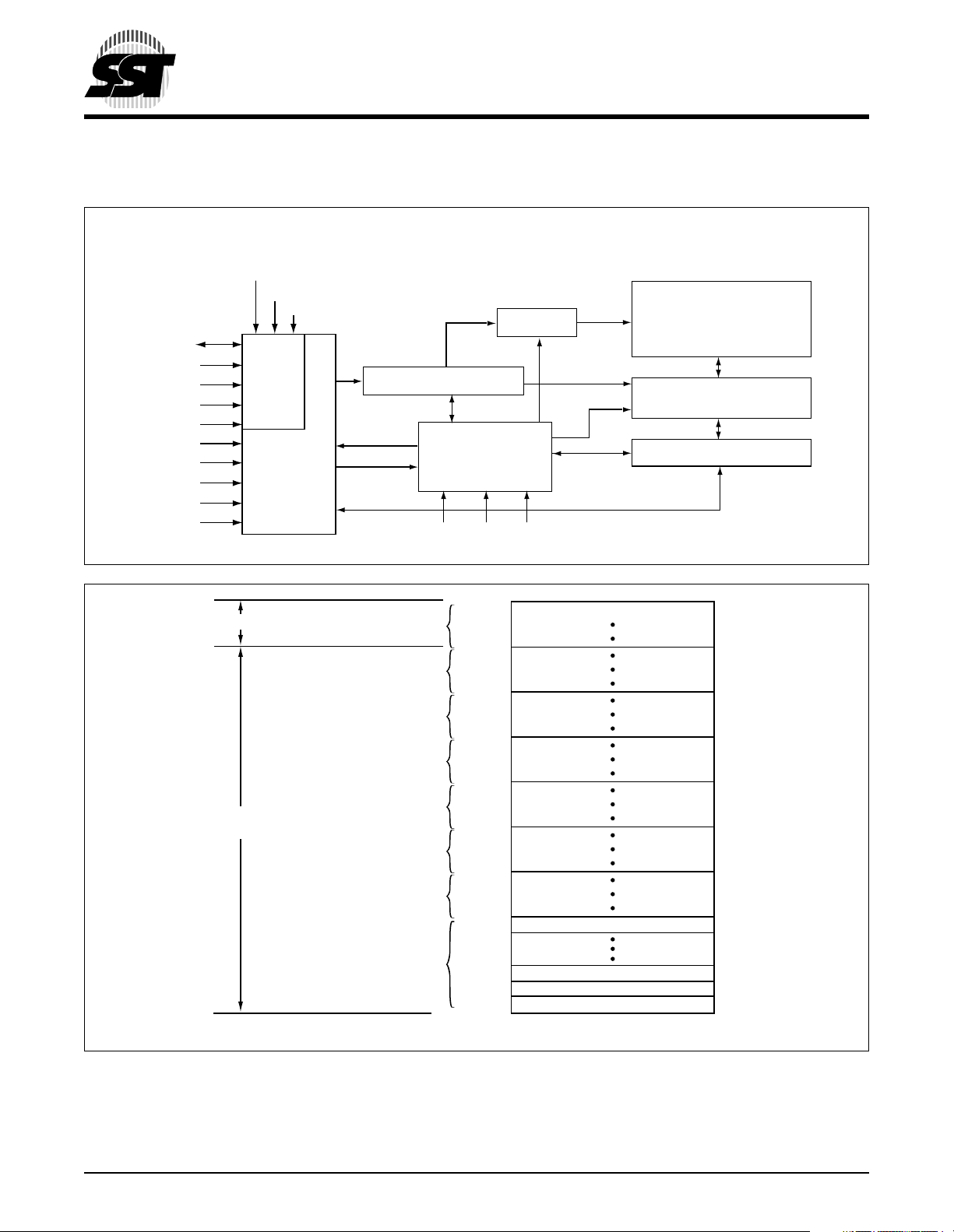
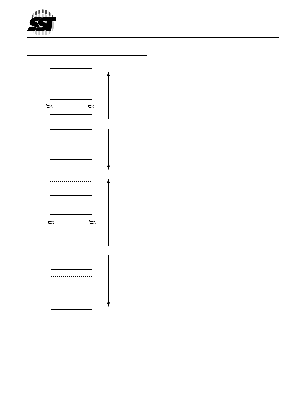
FUNCTIONAL BLOCKS
FUNCTIONAL BLOCK DIAGRAM
TBL#
WP#
LAD[3:0]
LCLK
LFRAME#
ID[3:0]
GPI[4:0]
R/C#
A[10:0]
DQ[7:0]
OE#
WE#
LPC
Interface
Programmer
Interface
INIT#
X-Decoder
Address Buffers & Latches
Control Logic
RST#
4 Mbit LPC Flash
SST49LF040
Advance Information
SuperFlash
Memory
Y-Decoder
I/O Buffers and Data Latches
CE#MODE
562 ILL B1.0
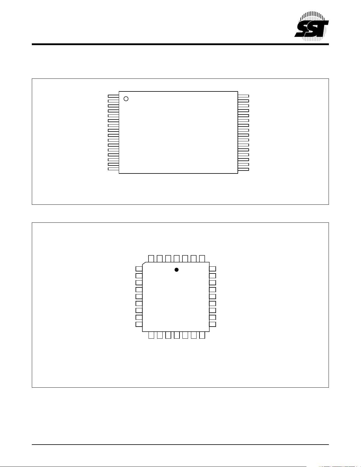
TBL#
Block 7
7FFFFH
70000H
6FFFFH
Block 6
60000H
5FFFFH
Block 5
50000H
4FFFFH
Block 4
40000H
3FFFFH
Block 3
WP#
30000H
2FFFFH
Block 2
20000H
1FFFFH
Block 1
10000H
0F000H
0EFFFH
Block 0
(64 KByte)
03000H
02000H
01000H
00000H
FIGURE 1: DEVICE MEMORY MAP FOR SST49LF040
Boot Block
4 KByte Sector 15
4 KByte Sector 2
4 KByte Sector 1
4 KByte Sector 0
562 ILL F03.0
©2001 Silicon Storage Technology, Inc. S71213-00-000 11/01 562
6
4 Mbit LPC Flash
SST49LF040
Advance Information
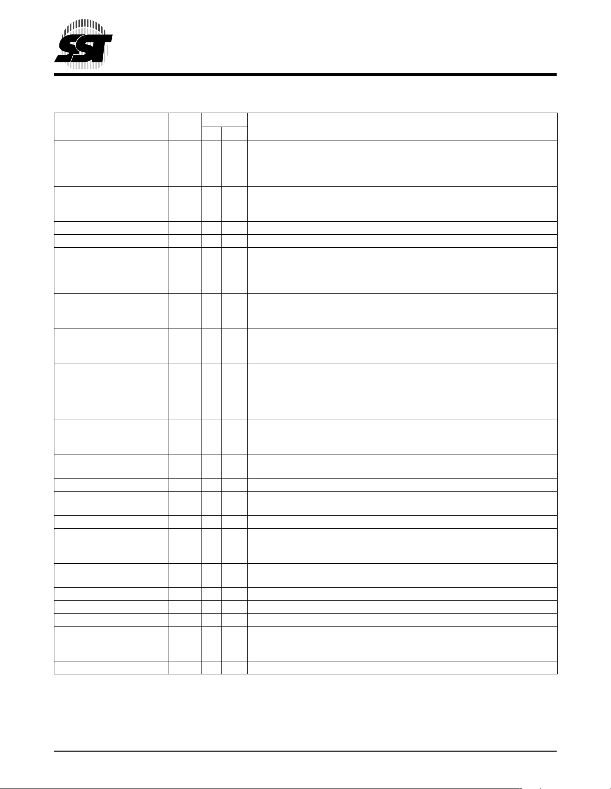
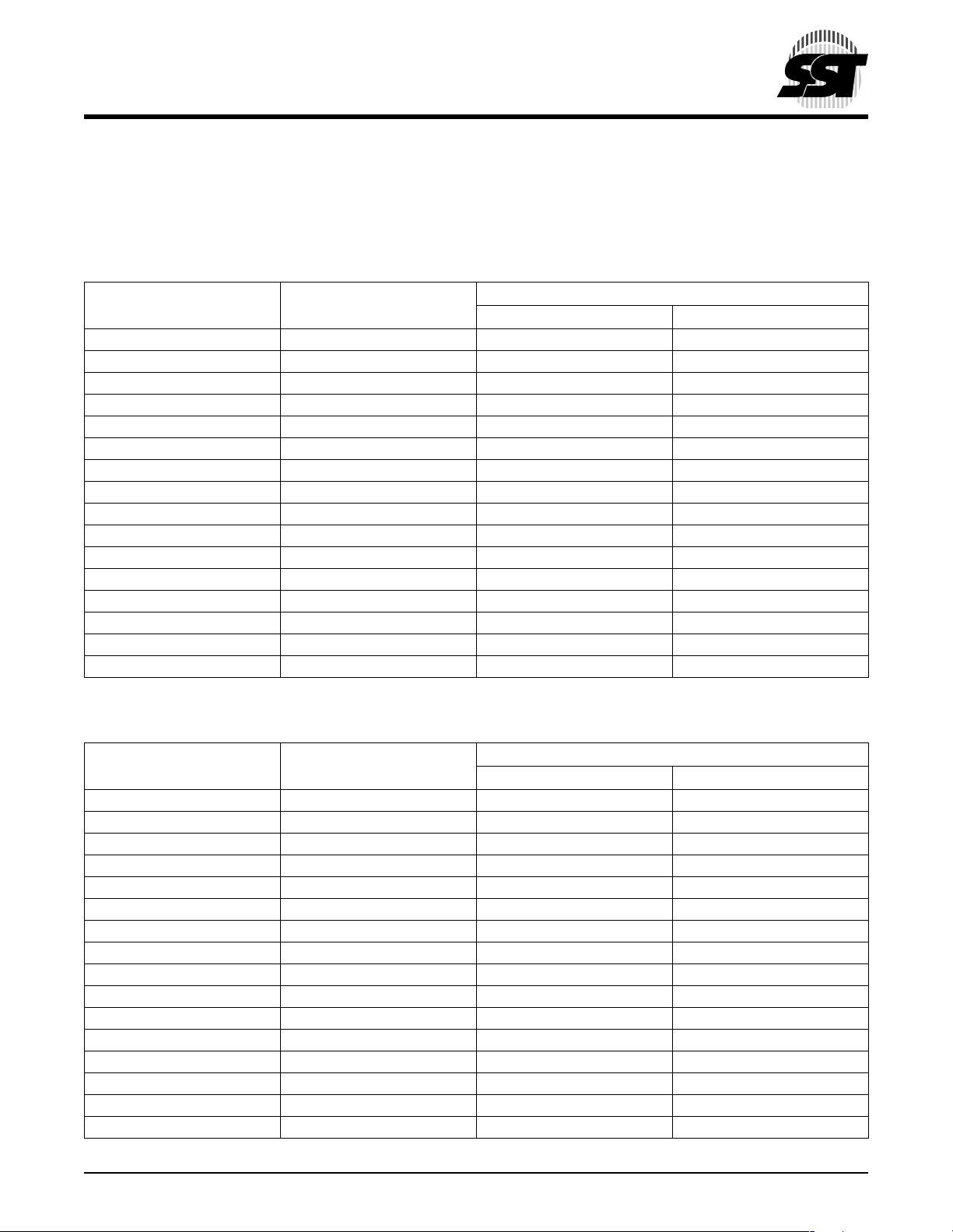
PIN DESCRIPTION
NC
NC
NC
NC (CE#)
MODE (MODE)
A10 (GPI4)
R/C# (LCLK)
V
DD (VDD
NC
RST# (RST#)
A9 (GPI3)
A8 (GPI2)
A7 (GPI1)
A6 (GPI0)
A5 (WP#)
A4 (TBL#)
1
2
3
4
5
6
7
)
8
9
10
11
12
13
14
15
16
Standard Pinout
Top View
Die Up
( ) Designates LPC Mode
FIGURE 2: PIN ASSIGNMENTS FOR 32-LEAD TSOP (8MM X 14MM)
)
DD
(V
DD
R/C# (LCLK)
A10 (GPI4)
29
28
27
26
25
24
23
22
21
A7(GPI1)
A6 (GPI0)
A5 (WP#)
A4 (TBL#)
A3 (ID3)
A2 (ID2)
A1 (ID1)
A0 (ID0)
DQ0 (LAD0)
A8 (GPI2)
A9 (GPI3)
RST# (RST#)NCV
4 3 2 1 32 31 30
5
6
7
8
32-lead PLCC
9
10
Top View
11
12
13
14 15 16 17 18 19 20
32
31
30
29
28
27
26
25
24
23
22
21
20
19
18
17
562 ILL F03a.0
MODE (MODE)
NC (CE#)
NC
NC
VDD (VDD)
OE# (INIT#)
WE# (LFRAME#)
NC
DQ7 (RES)
OE# (INIT#)
WE# (LFRAME#)
V
)
DD (VDD
DQ7 (RES)
DQ6 (RES)
DQ5 (RES)
DQ4 (RES)
DQ3 (LAD3)
V
)
SS (VSS
DQ2 (LAD2)
DQ1 (LAD1)
DQ0 (LAD0)
A0 (ID0)
A1 (ID1)
A2 (ID2)
A3 (ID3)
)
SS
(V
SS
V
DQ4 (RES)
DQ5 (RES)
DQ1 (LAD1)
DQ3 (LAD3)
DQ2 (LAD2)
( ) Designates LPC Mode
FIGURE 3: P
©2001 Silicon Storage Technology, Inc. S71213-00-000 11/01 562
IN ASSIGNMENTS FOR 32-LEAD PLCC
DQ6 (RES)
562 ILL F03b.0
7
4 Mbit LPC Flash
SST49LF040
Advance Information
TABLE 1: PIN DESCRIPTION
Interface
Symbol Pin Name Type
A10-A
Address I X Inputs for low-order addresses during Read and Write operations. Addresses are
0
DQ7-DQ0Data I/O X To output data during Read cycles and receive input data during Write cycles.
OE# Output Enable I X To gate the data output buffers.
WE# Write Enable I X To control the Write operations.
MODE Interface
Mode Select
INIT# Initialize I X This is the second reset pin for in-system use. This pin is internally combined
ID[3:0]
or
Identification
Inputs
ID[3:1]
GPI[4:0] General
Purpose Inputs
TBL# Top Block Lock I X When low, prevents programming to the boot block sectors at top of memory.
LAD[3:0] Address and
Data
LCLK Clock I X To provide a clock input to the control unit
LFRAME# Frame I X To indicate start of a data transfer operation; also used to abort an LPC cycle
RST# Reset I X X To reset the operation of the device
WP# Write Protect I X When low, prevents programming to all but the highest addressable blocks.
R/C# Row/Column
Select
RES Reserved X These pins must be left unconnected.
V
DD
V
SS
Power Supply PWR X X To provide power supply (3.0-3.6V)
Ground PWR X X Circuit ground (0V reference)
CE# Chip Enable I X This signal must be asserted to select the device. When CE# is low, the device
NC No Connection I X X Unconnected pins.
1. I=Input, O=Output
1
FunctionsPP LPC
internally latched during a Write cycle. For the programming interface, these
addresses are latched by R/C# and share the same pins as the high-order
address inputs.
Data is internally latched during a Write cycle. The outputs are in tri-state when
OE# is high.
I X X This pin determines which interface is operational. When held high, programmer
mode is enabled and when held low, LPC mode is enabled. This pin must be
setup at power-up or before return from reset and not change during device operation. This pin must be held high (V
) for PP mode and low (VIL) for LPC mode.
IH
with the RST# pin; If this pin or RST# pin is driven low, identical operation is
exhibited.
I X These four pins are part of the mechanism that allows multiple parts to be attached
to the same bus. These pins are internally pulled-down with a resistor between 20100 KΩ
I X These individual inputs can be used for additional board flexibility. The state of
these pins can be read through LPC registers. These inputs should be at their
desired state before the start of the PCI clock cycle during which the read is
attempted, and should remain in place until the end of the Read cycle. Unused
GPI pins must not be floated.
When TBL# is high it disables hardware write protection for the top block sectors.
This pin cannot be left unconnected.
I/O X To provide LPC control signals, as well as addresses and Command
Inputs/Outputs data.
in progress.
When WP# is high it disables hardware write protection for these blocks.
This pin cannot be left unconnected.
I X Select for the Programming interface, this pin determines whether the address
pins are pointing to the row addresses, or to the column addresses.
is enabled. CE# must remain low during internal Write (Program or Erase)
operations. When CE# is high, the device is placed in low power Standby mode.
T1.4 562
©2001 Silicon Storage Technology, Inc. S71213-00-000 11/01 562
8

4 Mbit LPC Flash
SST49LF040
Advance Information
MODE SELECTION
The SST49LF040 flash memory devices can operate in
two distinct interface modes: the LPC mode and the Parallel Programming (PP) mode. The mode pin is used to set
the interface mode selection. If the mode pin is set to logic
High, the device is in PP mode; while if the mode pin is set
Low, the device is in the LPC mode. The mode selection
pin must be configured prior to device operation. The mode
pin is internally pulled down if the pin is left unconnected. In
LPC mode, the device is configured to its host using standard LPC interface protocol. Communication between Host
and the SST49LF040 occurs via the 4-bit I/O communication signals, LAD [3:0] and LFRAME#. In PP mode, the
device is programmed via an 11-bit address and an 8-bit
data I/O parallel signals. The address inputs are multiplexed in row and column selected by control signal R/C#
pin. The row addresses are mapped to the higher internal
addresses, and the column addresses are mapped to the
lower internal addresses. See Figure 1, the Device Memory Map, for address assignments.
LPC MODE
CE#
The CE# pin, enables and disables the SST49LF040, controlling Read and Write access of the device. To enable the
SST49LF040, the CE# pin must be driven low one clock
cycle prior to LFRAME# being driven low. CE# must
remain active low during internal Write (Erase or Program)
operations. The device will enter the Standby mode when
internal Write operations are completed and CE# is high.
LFRAME#
The LFRAME# signifies the start of a frame or the termination of a broken frame. Asserting LFRAME# for one or
more clock cycle and driving a valid START value on
LAD[3:0] will initiate device operation. The device will enter
the Standby mode when internal operations are completed
and LFRAME# is high.
Device Memory Hardware Write Protection
The Top Boot Lock (TBL#) and Write Protect (WP#) pins
are provided for hardware write protection of device memory in the SST49LF040. The TBL# pin is used to write protect 16 boot sectors (64 KByte) at the highest memory
address range for the SST49LF040. WP# pin write protects the remaining sectors in the flash memory.
An active low signal at the TBL# pin prevents Program and
Erase operations of the top boot sectors. When TBL# pin is
held high, the write protection of the top boot sectors is disabled. The WP# pin serves the same function for the
remaining sectors of the device memory. The TBL# and
WP# pins write protection functions operate independently
of one another.
Both TBL# and WP# pins must be set to their required protection states prior to starting a Program or Erase operation. A logic level change occurring at the TBL# or WP# pin
during a Program or Erase operation could cause unpredictable results.
Reset
A VIL on INIT# or RST# pin initiates a device reset. INIT#
and RST# pins have the same function internally. It is
required to drive INIT# or RST# pins low during a system
reset to ensure proper CPU initialization. During a Read
operation, driving INIT# or RST# pins low deselects the
device and places the output drivers, LAD[3:0], in a highimpedance state. The reset signal must be held low for a
minimal duration of time T
a reset procedure is performed during a Program or Erase
operation. See Table 14, Reset Timing Parameters, for
more information. A device reset during an active Program
or Erase will abort the operation and memory contents may
become invalid due to data being altered or corrupted from
an incomplete Erase or Program operation.
. A reset latency will occur if
RSTP
Device Operation
The LPC mode uses a 5-signal communication interface, a
4-bit address/data bus, LAD[3:0], and a control line,
LFRAME#, to control operations of the SST49LF040.
Cycle type operations such as Memory Read and Memory
Write are defined in Intel Low Pin Count Interface Specification, Revision 1.0. JEDEC Standard SDP (Software
Data Protection) Program and Erase commands
sequences are incorporated into the standard LPC memory cycles. See Figure 12 through Figure 17 timing diagrams for command sequences.
LPC signals are transmitted via the 4-bit Address/Data bus
(LAD[3:0]), and follow a particular sequence, depending on
whether they are Read or Write operations. The standard
LPC memory cycle is defined in Table 18.
Both LPC Read and Write operations start in a similar way
as shown in Figures 10 and 11 timing diagrams. The host
(which is the term used here to describe the device driving
©2001 Silicon Storage Technology, Inc. S71213-00-000 11/01 562
9

4 Mbit LPC Flash
SST49LF040
Advance Information
the memory) asserts LFRAME# for one or more clocks
and drives a start value on the LAD[3:0] bus.
At the beginning of an operation, the host may hold the
LFRAME# active for several clock cycles, and even change
the Start value. The LAD[3:0] bus is latched every rising
edge of the clock. On the cycle in which LFRAME# goes
inactive, the last latched value is taken as the Start value.
CE# must be asserted one cycle before the start cycle to
select the SST49LF040 for Read and Write operations.
Once the SST49LF040 identifies the operation as valid (a
start value of all zeros), it next expects a nibble that indicates whether this is a memory Read or Write cycle. Once
this is received, the device is now ready for the Address
and Data cycles. For Write operation the Data cycle will follow the Address cycle, and for Read operation TAR and
SYNC cycles occur between the Address and Data cycles.
At the end of every operation, the control of the bus must
be returned to the host by a 2-clock TAR cycle.
Abort Mechanism
If LFRAME# is driven low for one or more clock cycles during a LPC cycle, the cycle will be terminated and the device
will wait for the ABORT command. The host must drive the
LAD[3:0] with ‘1111b’ (ABORT command) to return the
device to the ready mode. If abort occurs during the internal write cycle, the data may be incorrectly programmed or
erased. It is required to wait for the Write operation to complete prior to initiation of the abort command. It is recommended to check the write status with Data# Polling D[7] or
Toggle Bit D[6]. One other option is to wait for the fixed write
time to expire.
Write Operation Status Detection
The SST49LF040 device provides two software means to
detect the completion of a Write (Program or Erase) cycle,
in order to optimize the system write cycle time. The software detection includes two status bits: Data# Polling D[7]
and Toggle Bit D[6]. The End-of-Write detection mode is
incorporated into the LPC Read Cycle. The actual completion of the nonvolatile write is asynchronous with the system; therefore, either a Data# Polling or Toggle Bit read
may be simultaneous with the completion of the Write
cycle. If this occurs, the system may possibly get an erroneous result, i.e., valid data may appear to conflict with either
D[7] or D[6]. In order to prevent spurious rejection, if an
erroneous result occurs, the software routine should
include a loop to read the accessed location an additional
two (2) times. If both Reads are valid, then the device has
completed the Write cycle, otherwise the rejection is valid.
Data# Polling
When the SST49LF040 device is in the internal Program
operation, any attempt to read D[7] will produce the complement of the true data. Once the Program operation is
completed, D[7] will produce true data. Note that even
though D[7] may have valid data immediately following the
completion of an internal Write operation, the remaining
data outputs may still be invalid: valid data on the entire
data bus will appear in subsequent successive Read
cycles. During internal Erase operation, any attempt to
read D[7] will produce a ‘0’. Once the internal Erase operation is completed, D[7] will produce a ‘1’. Proper status will
not be given using Data# Polling if the address is in the
invalid range.
Toggle Bit
During the internal Program or Erase operation, any consecutive attempts to read D[6] will produce alternating 0s and
1s, i.e., toggling between 0 and 1. When the internal Program or Erase operation is completed, the toggling will stop.
System Memory Mapping
The LPC address sequence is 32 bits long. The
SST49LF040 will respond to addresses mapped into the
top of the 4GB memory space from FFFF FFFFH to
FF00 0000H or bottom of the 4GB memory space from
00000 000H to 00FF FFFFFH. Address bits A
decoded as memory addresses for SST49LF040, A
are device ID strapping bits, A23 directs Reads and Writes
to memory locations (A
tions (A
Refer to Multiple Device Selection for more detail in device
ID strapping decoding. Refer to Figures 4 and 5 for System
Memory Boot Configuration.
23
= 0).
= 1) or to register access loca-
23
18-A0
are
22-A19
Multiple Device Selection
Multiple LPC Flash devices may be strapped to increase
memory densities in a system. The four ID strapping pins,
ID[3:0], allow up to 16 devices to be attached to the same
bus by using different ID strapping in a system. Equal density must be used with multiple devices. BIOS support, bus
loading or the attaching bridge may limit this number. The
maximum “window” of the LPC array visible at one time is
16 MByte.
Applications that boot from the top address of the 4 GByte
system memory map; the ID strapping is sequentially
incremented downward as shown in Figure 4. For applications that boot from the bottom address of the 4 GByte system memory map, the ID strapping increments upward but
non-sequentially as shown in Figure 5.
©2001 Silicon Storage Technology, Inc. S71213-00-000 11/01 562
10
4 Mbit LPC Flash
SST49LF040
Advance Information
With hardware strapping, ID bits in the address field is
included in every LPC address memory cycle. The address
bits [A22: A19] are used to select the device with proper
IDs. The ID strapping bits in the address field will be
decoded depending on where the device is mapped on the
4 GByte system memory map. See Table 2 for ID address
bits decoding. The device will compare these bits with
ID[3:0]’s strapping values. If there is a mismatch, the device
will ignore the remainder of the cycle.
TABLE 2: ID STRAPPING VALUES FOR SST49LF040
Address Bits [A
Decoding
Device #
Hardware
Strapping
4 GByte System Memory
ID[3:0] Top Bottom
0 (Boot device) 0000 1111b 0001b
1 0001 1110b 0000b
2 0010 1101b 0011b
3 0011 1100b 0010b
4 0100 1011b 0101b
5 0101 1010b 0100b
6 0110 1001b 0111b
7 0111 1000b 0110b
8 1000 0111b 1001b
9 1001 0110b 1000b
10 1010 0101b 1011b
11 1011 0100b 1010b
12 1100 0011b 1101b
13 1101 0010b 1100b
14 1110 0001b 1111b
15 1111 0000b 1110b
1. Address bits A22-A19 decoding for multiple device selection
depends on whether the device is mapped from the top of the
4GB system memory map or from the bottom of the 4GB
system memory map.
22-A19
1
T2.3 562
]
(Boot Block)
Boot Device #0
(Boot Block)
Device #1
(Boot Block)
Device #2
(Boot Block)
Device #3
(Boot Block)
Device #14
(Boot Block)
Device #15
Device #0
Device #1
Device #2
Device #3
FFFF FFFFH
8 MByte
Memory Access
FF80 0000H
FF7F FFFFH
8 MByte
Register Access
Device #14
Device #15
FF00 0000H
562 ILL F01.1
FIGURE 4: B
©2001 Silicon Storage Technology, Inc. S71213-00-000 11/01 562
OOT CONFIGURATION FROM THE TOP
OF THE 4 GBYTE SYSTEM MEMORY MAP
11
Device #14
Device #15
Device #2
Device #3
Device #0
Device #1
(Boot Block)
Device #14
(Boot Block)
Device #15
(Boot Block)
Device #2
(Boot Block)
00FF FFFFH
8 MByte
Register Access
0080 0000H
007F FFFFH
8 MByte
Memory Access
4 Mbit LPC Flash
SST49LF040
Advance Information
Registers
There are two registers available on the SST49LF040, the
General Purpose Inputs Registers (GPI_REG) and the
JEDEC ID Registers. Since multiple LPC memory devices
may be used to increase memory densities, these registers
appear at its respective address location in the 4 GByte
system memory map. Unused register locations will read
as 00H. Any attempt to read registers during internal Write
operation will respond as “Write Operation Status Detection” (Data# Polling or Toggle Bit). Tables 4 and 5 list
GPI_REG and JEDEC ID address locations for
SST49LF040 with its respective device strapping.
TABLE 3: GENERAL PURPOSE INPUTS REGISTER
Pin #
Bit Function
7:5 Reserved - -
4GPI[4]
Reads status of general
purpose input pin
3GPI[3]
Reads status of general
purpose input pin
2GPI[2]
Reads status of general
purpose input pin
1GPI[1]
Reads status of general
purpose input pin
0GPI[0]
Reads status of general
purpose input pin
32-PLCC 32-TSOP
30 6
311
412
513
614
T3.1 562
Device #3
(Boot Block)
Boot Device #0
(Boot Block)
Device #1
0000 0000H
562 ILL F02.3
General Purpose Inputs Register
The GPI_REG (General Purpose Inputs Register) passes
the state of GPI[4:0] pins at power-up on the SST49LF040.
It is recommended that the GPI[4:0] pins be in the desired
state before LFRAME# is brought low for the beginning of
the next bus cycle, and remain in that state until the end of
the cycle. There is no default value since this is a passthrough register. See Table 3, General Purpose Inputs
Register, for the GPI_REG bits and functions and Tables 4
and 5 for memory address location for its respective device
strapping.
FIGURE 5: BOOT CONFIGURATION FROM THE
BOTTOM OF THE 4 GBYTE SYSTEM
EMORY MAP
M
©2001 Silicon Storage Technology, Inc. S71213-00-000 11/01 562
12
4 Mbit LPC Flash
SST49LF040
Advance Information
JEDEC ID Registers
The JEDEC ID registers identify the device as
SST49LF040 and manufacturer as SST in LPC mode. See
tive JEDEC ID location. Register is not available for Read
when the device is in Erase/Program operation. Unused
register locations will read as 00H.
Tables 4 and 5 for memory address location for its respec-
TABLE 4: MEMORY MAP REGISTER ADDRESSES (TOP OF THE 4GB SYSTEM MEMORY)
JEDEC ID
Device # GPI_REG
0 FF7C 0100H FF7C 0000H FF7C 0001H
1 FF74 0100H FF74 0000H FF74 0001H
2 FF6C 0100H FF6C 0000H FF6C 0001H
3 FF64 0100H FF64 0000H FF64 0001H
4 FF5C 0100H FF5C 0000H FF5C 0001H
5 FF54 0100H FF54 0000H FF54 0001H
6 FF4C 0100H FF4C 0000H FF4C 0001H
7 FF44 0100H FF44 0000H FF44 0001H
8 FF3C 0100H FF3C 0000H FF3C 0001H
9 FF34 0100H FF34 0000H FF34 0001H
10 FF2C 0100H FF2C 0000H FF2C 0001H
11 FF24 0100H FF24 0000H FF24 0001H
12 FF1C 0100H FF1C 0000H FF1C 0001H
13 FF14 0100H FF14 0000H FF14 0001H
14 FF0C 0100H FF0C 0000H FF0C 0001H
15 FF04 0100H FF04 0000H FF04 0001H
Manufacturer Device
T4.5 554
TABLE 5: MEMORY MAP REGISTER ADDRESSES (BOTTOM OF THE 4GB SYSTEM MEMORY)
JEDEC ID
Device # GPI_REG
0 008C 0100H 008C 0000H 008C 0001H
1 0084 0100H 0084 0000H 0084 0001H
2 009C 0100H 009C 0000H 009C 0001H
3 0094 0100H 0094 0000H 0094 0001H
4 00AC 0100H 00AC 0000H 00AC 0001H
5 00A4 0100H 00A4 0000H 00A4 0001H
6 00BC 0100H 00BC 0000H 00BC 0001H
7 00B4 0100H 00B4 0000H 00B4 0001H
8 00CC 0100H 00CC 0000H 00CC 0001H
9 00C4 0100H 00C4 0000H 00C4 0001H
10 00DC 0100H 00DC 0000H 00DC 0001H
11 00D4 0100H 00D4 0000H 00D4 0001H
12 00EC 0100H 00EC 0000H 00EC 0001H
13 00E4 0100H 00E4 0000H 00E4 0001H
14 00FC 0100H 00FC 0000H 00FC 0001H
15 00F4 0100H 00F4 0000H 00F4 0001H
©2001 Silicon Storage Technology, Inc. S71213-00-000 11/01 562
13
Manufacturer Device
T5.5 554

4 Mbit LPC Flash
SST49LF040
Advance Information
PARALLEL PROGRAMMING MODE
Reset
Driving the RST# low will initiate a hardware reset of the
SST49LF040.
Device Operation
Commands are used to initiate the memory operation functions of the device. The data portion of the software command sequence is latched on the rising edge of WE#.
During the software command sequence the row address
is latched on the falling edge of R/C# and the column
address is latched on the rising edge of R/C#.
Read
The Read operation of the SST49LF040 device is controlled by OE#. OE# is the output control and is used to
gate data from the output pins. Refer to the Read cycle timing diagram, Figure 19, for further details.
Byte-Program Operation
The SST49LF040 device is programmed on a byte-by-byte
basis. Before programming, one must ensure that the sector in which the byte is programmed is fully erased. The
Byte-Program operation is initiated by executing a fourbyte-command load sequence for Software Data Protection with address (BA) and data in the last byte sequence.
During the Byte-Program operation, the row address (A
) is latched on the falling edge of R/C# and the column
A
0
address (A
) is latched on the rising edge of R/C#.
21-A11
The data bus is latched on the rising edge of WE#. The
Program operation, once initiated, will be completed, within
20 µs. See Figure 23 for Program operation timing diagram
and Figure 35 for its flowchart. During the Program operation, the only valid reads are Data# Polling and Toggle Bit.
During the internal Program operation, the host is free to
perform additional tasks. Any commands written during the
internal Program operation will be ignored.
Sector-Erase Operation
The Sector-Erase operation allows the system to erase the
device on a sector-by-sector basis. The sector architecture
is based on uniform sector size of 4 KByte. The SectorErase operation is initiated by executing a six-byte command load sequence for Software Data Protection with
Sector-Erase command (30H) and sector address (SA) in
the last bus cycle. The internal Erase operation begins after
the sixth WE# pulse. The End-of-Erase can be determined
using either Data# Polling or Toggle Bit methods. See Figure 24 for Sector-Erase timing waveforms. Any commands
written during the Sector-Erase operation will be ignored.
10
Block-Erase Operation
The Block-Erase Operation allows the system to erase the
device in 64 KByte uniform block size. The Block-Erase
operation is initiated by executing a six-byte command load
sequence for Software Data Protection with Block-Erase
command (50H) and block address. The internal BlockErase operation begins after the sixth WE# pulse. The
End-of-Erase can be determined using either Data# Polling
or Toggle Bit methods. See Figure 25 for Block-Erase timing waveforms. Any commands written during the BlockErase operation will be ignored.
Chip-Erase Operation
The SST49LF040 device provides a Chip-Erase operation,
which allows the user to erase the entire memory array to
the “1s” state. This is useful when the entire device must be
quickly erased.
The Chip-Erase operation is initiated by executing a sixbyte Software Data Protection command sequence with
Chip-Erase command (10H) with address 5555H in the last
byte sequence. The internal Erase operation begins with
the rising edge of the sixth WE#. During the internal Erase
operation, the only valid read is Toggle Bit or Data# Polling.
See Table 8 for the command sequence, Figure 26 for
Chip-Erase timing diagram, and Figure 38 for the flowchart.
Any commands written during the Chip-Erase operation
will be ignored.
-
Write Operation Status Detection
The SST49LF040 device provides two software means to
detect the completion of a Write (Program or Erase) cycle,
in order to optimize the system write cycle time. The software detection includes two status bits: Data# Polling
) and Toggle Bit (DQ6). The End-of-Write detection
(DQ
7
mode is enabled after the rising edge of WE# which initiates the internal Program or Erase operation.
The actual completion of the nonvolatile write is asynchronous with the system; therefore, either a Data# Polling or
Toggle Bit read may be simultaneous with the completion
of the Write cycle. If this occurs, the system may possibly
get an erroneous result, i.e., valid data may appear to conflict with either DQ
or DQ6. In order to prevent spurious
7
rejection, if an erroneous result occurs, the software routine
should include a loop to read the accessed location an
additional two (2) times. If both reads are valid, then the
device has completed the Write cycle, otherwise the rejection is valid.
©2001 Silicon Storage Technology, Inc. S71213-00-000 11/01 562
14
4 Mbit LPC Flash
SST49LF040
Advance Information
Data# Polling (DQ7)
When the SST49LF040 device is in the internal Program
operation, any attempt to read DQ
will produce the com-
7
plement of the true data. Once the Program operation is
completed, DQ
though DQ
will produce true data. Note that even
7
may have valid data immediately following the
7
completion of an internal Write operation, the remaining
data outputs may still be invalid: valid data on the entire
data bus will appear in subsequent successive Read
cycles after an interval of 1 µs. During internal Erase operation, any attempt to read DQ
internal Erase operation is completed, DQ
will produce a ‘0’. Once the
7
will produce a
7
‘1’. The Data# Polling is valid after the rising edge of fourth
WE# pulse for Program operation. For Sector-, Block-, or
Chip-Erase, the Data# Polling is valid after the rising edge
of sixth WE# pulse. See Figure 21 for the Data# Polling timing diagram and Figure 36 for a flowchart. Proper status will
not be given using Data# Polling if the address is in the
invalid range.
Toggle Bit (DQ
)
6
During the internal Program or Erase operation, any consecutive attempts to read DQ
will produce alternating 0s
6
and 1s, i.e., toggling between 0 and 1. When the internal
Program or Erase operation is completed, the toggling will
stop. The device is then ready for the next operation. The
Toggle Bit is valid after the rising edge of fourth WE# pulse
for Program operation. For Sector-, Block-, or Chip-Erase,
the Toggle Bit is valid after the rising edge of sixth WE#
pulse. See Figure 22 for the Toggle Bit timing diagram and
Figure 36 for a flowchart.
Data Protection
The SST49LF040 device provides both hardware and software features to protect nonvolatile data from inadvertent
writes.
Hardware Data Protection
Noise/Glitch Protection:
not initiate a Write cycle.
Power Up/Down Detection: The Write operation is
V
DD
inhibited when V
Write Inhibit Mode:
the Write operation. This prevents inadvertent writes during
power-up or power-down.
A WE# pulse of less than 5 ns will
is less than 1.5V.
DD
Forcing OE# low, WE# high will inhibit
Software Data Protection (SDP)
The SST49LF040 provides the JEDEC approved Software
Data Protection scheme for all data alteration operation,
i.e., Program and Erase. Any Program operation requires
the inclusion of a series of three-byte sequence. The threebyte load sequence is used to initiate the Program operation, providing optimal protection from inadvertent Write
operations, e.g., during the system power-up or powerdown. Any Erase operation requires the inclusion of a sixbyte load sequence. The SST49LF040 device is shipped
with the Software Data Protection permanently enabled.
See Table 8 for the specific software command codes. During SDP command sequence, invalid commands will abort
the device to Read mode, within T
RC.
Electrical Specifications
The AC and DC specifications for the LPC interface signals (LA0[3:0], LFRAME, LCLCK and RST#) as defined
in Section 4.2.2.4 of the PCI local Bus specification, Rev.
2.1. Refer to Table 9 for the DC voltage and current specifications. Refer to Tables 13 through 16 and Tables 19
through 21 for the AC timing specifications for Clock,
Read, Write, and Reset operations.
Product Identification
The Product Identification mode identifies the device as the
SST49LF040 and manufacturer as SST.
TABLE 6: P
Manufacturer’s ID 0000H BFH
Device ID
SST49LF040 0001H 51H
RODUCT IDENTIFICATION
Address Data
T6.1 562
Design Considerations
SST recommends a high frequency 0.1 µF ceramic capacitor to be placed as close as possible between V
less than 1 cm away from the VDD pin of the device.
V
SS
Additionally, a low frequency 4.7 µF electrolytic capacitor
from V
to VSS should be placed within 5 cm of the V
DD
pin. If you use a socket for programming purposes add an
additional 1-10 µF next to each socket.
The RST# pin must remain stable at V
for the entire dura-
IH
tion of an Erase operation. WP# must remain stable at V
for the entire duration of the Erase and Program operations
for non-boot block sectors. To write data to the top boot
block sectors, the TBL# pin must also remain stable at V
for the entire duration of the Erase and Program operations.
DD
and
DD
IH
IH
©2001 Silicon Storage Technology, Inc. S71213-00-000 11/01 562
15
 Loading...