

Silicon Storage Technology Inc SST49LF020-33-4C-WH, SST49LF020-33-4C-NH Datasheet

FEATURES:
2 Megabit LPC Flash
SST49LF020
SST49LF0202 Mb LPC Flash
Advance Information
• Standard LPC Interface
– Conforms to Intel LPC Interface Specification 1.0
• Organized as 256K x8
• Flexible Erase Capability
– Uniform 4 KByte sectors
– Uniform 16 KByte overlay blocks
– 16 KBytes Top boot block protection
– Chip-Erase for PP Mode
• Single 3.0-3.6V Read and Write Operations
• Superior Reliability
– Endurance: 100,000 Cycles (typical)
– Greater than 100 years Data Retention
• Low Power Consumption
– Active Read Current: 10 mA (typical)
– Standby Current: 10 µA (typical)
• Fast Sector-Erase/Byte-Program Operation
– Sector-Erase Time: 18 ms (typical)
– Block-Erase Time: 18 ms (typical)
– Chip-Erase Time: 70 ms (typical)
– Byte-Program Time: 14 µs (typical)
– Chip Rewrite Time: 4 seconds (typical)
– Single-pulse Program or Erase
– Internal timing generation
• Two Operational Modes
– Low Pin Count (LPC) Interface mo de f or
in-system operation
– Parallel Programming (PP) Mode f or f ast productio n
programming
• LPC Interface Mode
– 5-signal communication interface supporting
byte Read and Write
– 33 MHz clock frequency operation
– WP# and TBL# pins provide hardware write protect
for entire chip and/or t op boot b lo ck
– Standard SDP Command Set
– Data# Polling and Toggle Bit for
End-of-Write detection
– 5 GPI pins for system design flexibility
• Parallel Programming (PP) Mode
– 11 pin multiplexed address and
8 pin data I/O interface
– Supports fast In-System or PROM programming
for manufacturing
• CMOS I/O Compatibility
• Packages Available
– 32-lead PLCC
– 32- l ead TSOP (8mm x 14mm)
PRODUCT DESCRIPTION
The SST49LF020 flash memory device is designed to
interface with the LPC bus for PC and Int er ne t Appl ican ce
applications. It provides protection for the storage and
update of code and data in addition to adding system
design flexibility through five General Purpose Inputs (GPI).
The SST49LF020 is in compliance with Intel Low Pin
Count (LPC) Interface Specification 1.0. Two interface
modes are suppor te d: LPC Mode for In-Syste m programming and Parallel Programming (PP) Mode for fast factory
programming.
The SST49LF020 flash memory device is manufactured
with SST’s proprietary, high performance SuperFlash
Technology. The split-gate cell design and thick oxide
tunneling injector a ttain bette r reliabil ity and man uf actur ability compared with alternate approaches. The
SST49LF0 20 device signific antly improves per formance
and reliability, while lowering power consumption. The
SST49LF020 device writes (Program or Erase) with a
single 3.0-3.6V power supply. It uses less energy during
Erase and Program than alternative flash memory technologies. The tota l en er gy consu med is a func ti on o f the
applied vol tage , curr en t and time of ap plica tio n. Sinc e for
any give voltage range, the SuperFlash technology uses
less current to prog ram and ha s a shorter erase time , the
total energy consumed during any Erase or Program
operation is less than alternative flash memory technologies. The SST49LF020 product provides a maximum
Byte-Program time of 20µsec. The entire memory can be
erased and programmed byte-by-byte typically in 4 seconds, when using status detection features such as Toggle Bit or Data# Polling to indicate the completion of
Program oper at io n. Th e Sup erF lash te chno logy provides
fixed Erase and Program time, independent of the number of Erase/Program cycles that ha ve perf ormed. Therefore the system software or hardware does not have to
be calibrated or correlated to the cumulative number of
Erase/Program cycles as is necessary with alternative
flash memory technologies, whose Erase and Program
time increase with accum ul at ed Er ase/ Prog r a m cycl es .
To protect against inadvertent write, the SST49LF020
device has on-chip hardware and software data (SDP)
protection schemes . I t is o ffered with a typical endurance
of 100,000 cycles. Data retention is rated at greater than
100 years.
©2001 Silicon Storage Technology, Inc.
S71175-02-000 5/01 526
1
MPF is a trademark of Silicon Storage Technology, Inc. Intel is a registered trademark of Intel Corporation.
The SST logo and SuperFlash are registered trademarks of Silicon Storage Technology, Inc.
These specifications are subject to change without notice.

2 Megabit LPC Flash
SST49LF020
Advance Information
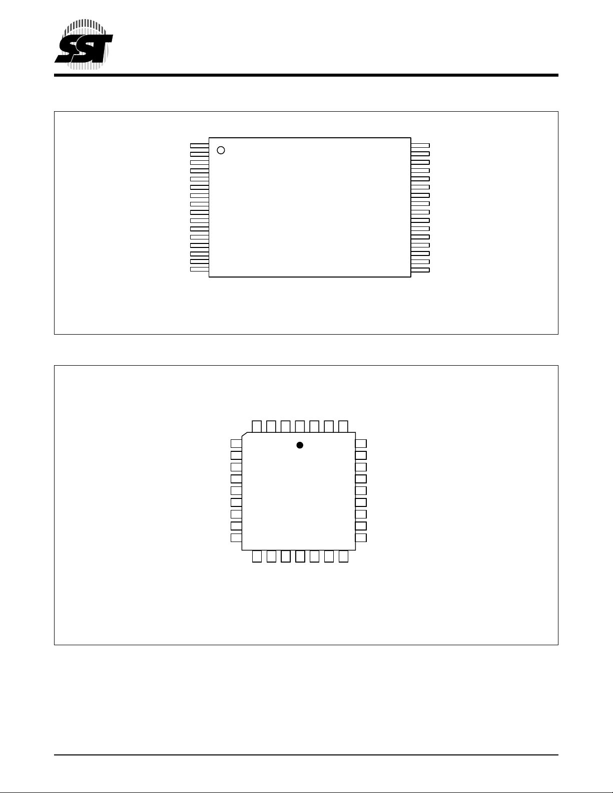
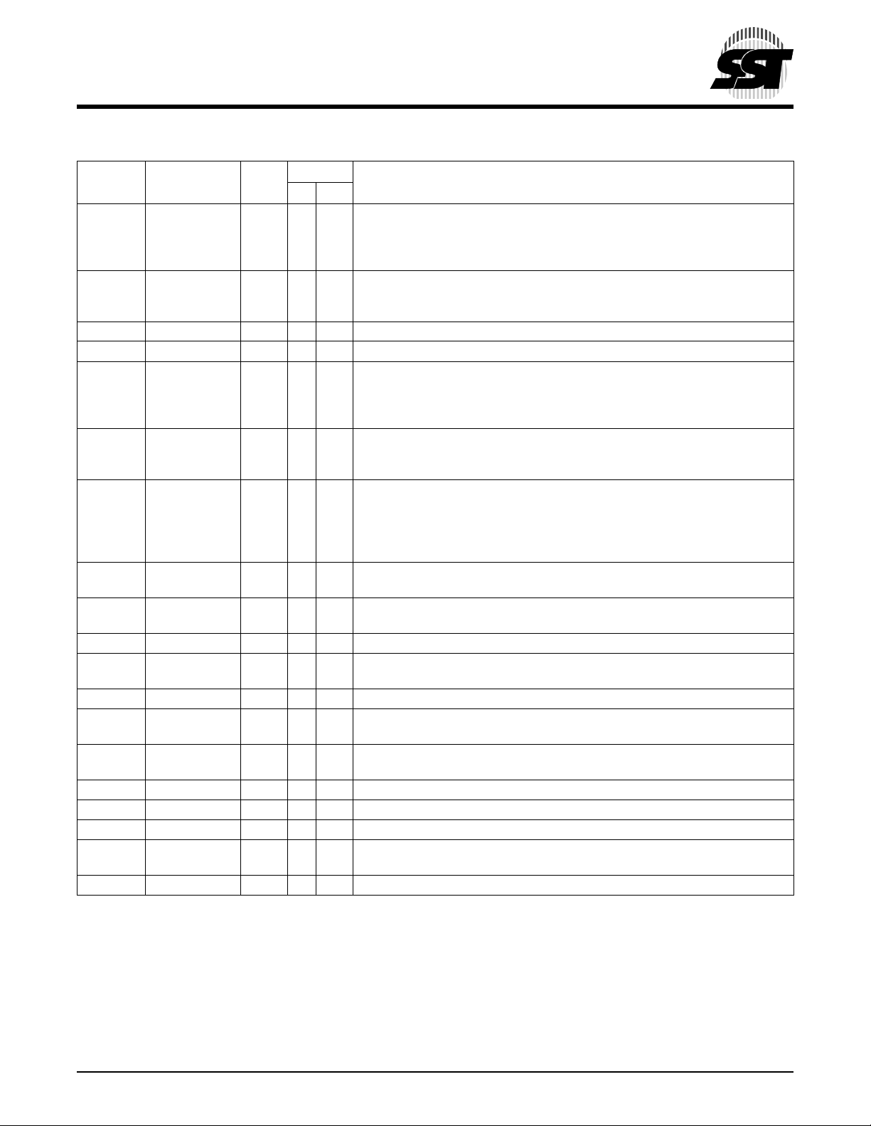
To meet high density, surface mount requirements, the
SST49LF020 device is offered in 32-lead TSOP and 32lead PLCC packages. See Figures 1 and 2 for pinouts and
Table 2 for pin descriptions.
Mode Selection and Description
The SST49LF020 flash memory device operates in two
distinct inter face modes: the LPC mode and the Parallel
Programming (PP) mode. The Mode pin is used to set the
interface mode selection. If the Mode pin is set to logic
High, the device is in PP mode; while if the Mode pin is set
Low, the device is in the LPC mode. The Mo de selection
pin must be configured prior to device operation.
In LPC mode, the device is configured to its host using
standard LPC interface protocol. Communication
between Host and the SST49LF020 occurs via the 4-bit
I/O communication signals, LAD [3:0] and LFRAME#.
In PP mode, the device is programmed via an 11-bit
address and an 8-bit data I/O parallel signals. The address
inputs are multiplexed in row and column sele ct ed by control signal R/C# pin. The row addresses are mapped to the
higher inter nal addresse s, and the colum n addresses a re
mapped to the lower internal addresses. See Device Memory Map for address assignments.
LPC MODE
Device Operation
The LPC mode uses a 5-s ignal co mmun icatio n interf ace , a
4-bit address/data bus, LAD[3:0], and a control line,
LFRAME#, to control operations of the SST49LF020.
Cycle type operations such as Memory Read and Memory
Write are defi ned in Intel Low Pi n Count Inte rface Specification, Revision 1.0. JEDEC Standard SDP (Software
Data Protection) Program and Erase commands
sequences are i ncorpo rated into the sta ndard LPC me mory cycles. See Figure 8 through Figure 13 timing diagrams
for command sequences.
LPC operations are tran smitted via the 4-bi t Add ress/ Data
bus (LAD[3:0]), and follow a par tic ular sequ ence, depen ding on whether they are Read or Write operations. The
standard LPC memory cycle is defined in Table 13.
Both LPC Read and Write operations start in a similar way
as shown in Figures 6 and 7 timing diagrams. The host
(which is the term used here to describe the device driving
the memory) asserts LFRAME# for one or more clocks
and drives a start value on the LAD[3:0] bus.
At the beginnin g of an operation, the host may hold the
LFRAME# activ e f or sev era l cloc k cycles , and e ven change
the Star t value. The LAD[3:0] bus is latched every risin g
edge of the clock. On the cycle in whic h LFRAME# goes
inactive, the last latched value is taken as the Start value.
CE# must be asserted on e cycle b efore the star t cy cle to
select the SST49LF020 for Read and Write operations.
Once the SST49LF020 identifies the operation as valid (a
start value of all zeros), it next expects a nibble that indicates
whether this is a memory read or program cycle. Once this
is received, the device is now ready for the Address and
Data cycles. For Program operati on the Data cycle will follow the Address cycle, and for Read operation TAR and
SYNC cycles occur between the Address and Data cycles.
At the end of ev ery operation, the control of the bus m ust be
returned to the host by a 2 clock TAR cycle.
Device Memory Hardware Write Protection
The Top Boot Lock (TBL#) and Write Protect (WP#) pins
are provided for hardware write protection of device
memory in the SST49LF020. The TBL# pin is used to
write protect four boot sectors (16 KBytes) at the highest
memory address range. WP# pin write protects the
remaining sectors in the flash memory.
An active low signal at the TBL# pin prevents Program and
Erase operations of the top boot sectors. When TBL# pin is
held high, the write protection of the top boot sectors is disabled. The WP# pin serves the same function for the
remaining sectors of the device memory. The TBL# and
WP# pins write protection functions operate independently
of one another.
Both TBL# and WP# pins must be set to their required
protection states prior to starting a Program or Erase
operation. A logic level change occurring at the TBL# or
WP# pin during a Program or Erase operation could
cause unpredictab le resul ts.
Reset
A VIL on INIT# or RST# pins initiates a device rese t. INI T#
and RST# pins have same function internally. It is required
to drive INIT# or RST# pins low dur ing a system reset to
ensure proper CPU initialization.
During a Read opera tion, driving IN IT# or RST# pins low
deselects the device and places the output drivers,
LAD[3:0], in a high-impedance state. The reset signal must
be held low for a minimal duration of time T
latency will occur if a reset procedure is performed during a
Program or Erase operation. See Table 12, Reset Timing
Param eters , for more information. A device rese t during an
active Program or Erase will abort the operation and mem-
RSTP .
A reset
©2001 Silicon Storage Technology, Inc. S71175-02-000 5/01 526
2
2 Megabit LPC Flash
SST49LF020
Advance Information
ory contents may become invalid due to data being altered
had been disr u pte d fr om an i nc om pl ete E rase or Pr o gram
operation.
ENERAL PURPOSE INPUTS REGISTER
G
Pin#
Bit Function
7:5 Reserved - -
4 GPI[4]
Reads status of
general purpose input pin
3 GPI[3]
Reads status of
general purpose input pin
2 GPI[2]
Reads status of
general purpose input pin
1 GPI[1]
Reads status of
general purpose input pin
0 GPI[0]
Reads status of
general purpose input pin
32-PLCC 32-TSOP
30 7
15
3
416
517
618
LFRAME#
The LFRAME# signifies the start of a frame or the termination of a broken frame. Asserting LFRAME# for one or
more clock cycle and driving a valid START value on
LAD[3:0] will initiate device operation. The device enters
standby mode when LF RAME# a nd C E# are h igh an d no
internal operations is in progress.
Abort Mechanism
If LFRAME# is driven low for one or more clock cycles during a LPC cycle, the cycle will be terminated and the device
will wait for the ABORT command. The host must drive the
LAD[3:0] with ‘1111b’ (ABORT command) to return the
device to the ready mode. If abor t o ccurs du ring the internal write cycle, the data may be incorrectly programmed or
erased. It is required to wait for the Write operation to complete prior to initiation of the abort com mand. It is recommended to check the write status with Data# Polling (DQ
or Toggle Bit (DQ
fixed write time to expire.
) pins. One other option is to wait for the
6
)
7
Registers
There is one register available on the SST49LF020. T he
General Purpose Inputs Register. This register appears
at its respective address location in the 4 GByte system
memory map.
General Purpose Inputs Register
The GPI_REG (General Purpose Inputs Register)
passes the state of GPI[4:0] pins at power-up on the
SST49LF020. It is recommended that the GPI[4:0] pins
be in the desired state before LFRAME# is brought low
for the beg inning of the ne xt b us cycle, and remain i n that
state until the end of the cycle. There is no default value
since this is a pass-through register. The GPI register
appears at FFBC0100H in the 4 GByte s system memory
map. See General Purpose Inputs Register table for the
GPI_REG bits and f uncti o n.
CE#
The CE# pin, enables and disables the SST49LF020, controlling read and wr ite acc ess of the d evice. To enable the
SST49LF020, the CE# pin must be driven low one cycle
prior to LFRAME# being driven low. F or write (erase or program) cy cles, th e CE# pin must rema in low during the i nternal programming. W hen CE# is high, the SST49LF0 20 is
placed in low-power standby-mode.
©2001 Silicon Storage Technology, Inc. S71175-02-000 5/01 526
3

PARALLEL PROGRAMMING MODE
2 Megabit LPC Flash
SST49LF020
Advance Information
Device Operation
Commands are used to initiate the memory operation functions of the device. The da ta por tion of th e software co mmand sequence is latched on the rising edge of WE#.
During the sof tware comman d sequenc e the row addr ess
is latched on the falling edge of R/C# and the column
address is latched on the rising edge of R/C#.
Read
The Read operation of the SST49LF020 device is controlled by OE#. OE# is the output control and is used to
gate data from the output pins. Refer to the Read cycle
timing diagram, Fi gure 15, f or further details .
Reset
Driving the RST# low will initiate a hardware reset of the
SST49LF020.
Byte-Program Operation
The SST49LF020 device is programmed on a byte-by-byte
basis. The Byte-Program operation is initiated by executing
a four-byte-command load sequence f or Software Data Protection with address (BA) and data in the last byte
sequence. During the Byte-Program operation, the row
address (A
the column address (A
of R/C#. The data bus is latched on the rising edge of WE#.
The Program operation, once initiated, will be completed,
within 20 µs. See Figures 7 and 19 for Program operation
timing diagram and Figure 31 for its flowchar t. During the
Program operation, the only valid reads are Data# Polling
and Toggle Bit. During the internal Program operation, the
host is free to perform additional tasks. Any commands written during the internal Program operation will be ignored.
) is latched on the falling edge of R/C# and
10-A0
) is latched on the rising edge
21-A11
Sector-Erase Operation
The Sector-Erase operation allows the system to erase
the device on a sector-by-sector basis. The sector architecture is based on uniform sector size of 4 KByte. The
Sector-Erase operation is initiated b y executing a six-bytecommand load sequence for Software Data Protection
with Sector-Erase command (30H) and sector address
(SA) in the last bus cycle. The internal Erase operation
begins after the sixth WE# pulse. The E nd-of-Erase can
be determined using either Data# Polling or Toggle Bit
methods. See Figure 20 for Sector-Erase timing waveforms. Any commands written during the Sector-Erase
operation will be ignored.
Block-Erase Ope ration
The Block-Erase Operation allo ws the system to erase the
device in 16 KByte unifor m block size. The Block-Erase
operation is initiated by executing a six-byte-command
load sequence for Software Data Protection with BlockErase command (50H) and block address. The internal
Block-Erase operation begins after the sixth WE# pulse.
The End-of-Erase can be determined using either Data#
Polling or Toggle Bit methods. See Figure 21 for BlockErase timing waveforms. Any commands written during
the Block-Erase operatio n will be ignored.
Chip-Erase
The SST49LF020 device p rovide s a C hip- Era se operation
only in PP Mode, which allows the user to erase the entire
memory array to the “1” state. This is useful when the entire
device must be quickly erased.
The Chip-Erase operation is initiated by executing a sixbyte Software Data Protection command sequence with
Chip-Erase command (10H) with address 5555H in the last
byte sequence. The inter nal Erase operation beg ins with
the rising edge of the sixth WE#. During the internal Erase
operation, the only valid read is T oggle Bit or Data# Polling.
See Table 4 for the command sequence, Figure 22 for
Chip-Erase timing diagram, and Figure 34 for the flowchart.
Any commands written during the Chip-Erase operation
will be ignored.
Write Operation Status Detection
The SST49LF020 device provides two software means
to detect the completion of a Write (Program or Erase)
cycle, in order to optimize the system write cycle time.
The software detection includes two status bits: Data#
Polling (DQ
detection mode is enabled after the rising edge of WE#
which initiates the in ternal Prog r am o r Er ase op er at ion .
The actual completion of the nonvolatile write is asynchronous with the system; therefore, either a Data# Polling or Toggle Bit read may be simultaneous with the
completion of the Write cycle. If this occurs, the system
may possibly g et an er rone ous re sult, i. e . , valid data may
appear to conflict w it h ei th er D Q
vent spurious rejection, if an erroneous result occurs, the
software routine should include a loop to read the
accessed location an additional two (2) times. If both
reads are valid, then the device has completed the Write
cycle, otherwise the reje ctio n is valid.
) and Toggle Bit (DQ6). The End-of-Write
7
or DQ6. In order to p re-
7
©2001 Silicon Storage Technology, Inc. S71175-02-000 5/01 526
4
2 Megabit LPC Flash
SST49LF020
Advance Information
Data# Polling (DQ7)
When the SST49LF02 0 device is in the interna l Program
operation, any attemp t to read DQ
will produce the com-
7
plement of the tru e data. Once the Program operation is
completed, DQ
will produce true data. T he device is then
7
ready for the next operation. Dur ing inter nal Erase ope ration, any attempt to read DQ
internal Erase operation is compl eted, DQ
will produce a ‘0’. Once the
7
will produce a
7
‘1’. The Data# Polling is valid after the rising edge of fourth
WE# pulse for Program o peration. For Sector-, Block- or
Chip-Erase, the Data# Polling is valid after the r ising edge
of sixth WE# pulse. See Figures 9 and 17 for Data# Polling
timing diagram and Figure 33 for a flowchart.
Toggle Bit (DQ6)
During the inter nal Program or Erase ope ration, any consecutive attempts to read DQ
will produce alternating “0”
6
and “1”, i.e., to ggli ng be tween “0” and “1”. When the inter-
nal Program or Erase operatio n is comp leted , the toggl ing
will stop. The device is then ready for the next operation.
The Toggle Bit is valid after the risi ng edge of four th WE#
pulse for Program operation. For Sector- , Block- or ChipErase, th e Toggle Bit is valid after the rising edge of sixth
WE# pulse. See Figures 10 and 18 for Toggle Bit timing
diagram and Figure 32 for a flowchart.
Data Protection
The SST49LF020 device provides both hardware and software features to protect nonvolatile d ata from inadverten t
writes.
Hardware Data Protection
Noise/Glitch Protection: A WE# pulse of less than 5 ns will
not initiate a Write cycl e.
six byte load sequence. The SST49LF020 device is
shipped with the Software Data Protection permanently
enabled. See Ta ble 4 for the specific software command
codes. During SDP command sequence, invalid commands will abort the device to read mode, within T
RC
.
Electrical Specifications
The AC and DC specifications for the LPC interface signals
(LAD[3:0], LCLCK. LFRAME# and RST#) as defined in
Section 4.2.2 of the “PCI Local Bus specification, Rev. 2.1”.
Refer to Table 5 for the DC voltage and current specifications. Refer to Tables 11, 12, 14, and 15 for the AC timing
specifications for Clock, Read, Program, Erase and Reset
operations.
Product Identification Mode
The product identification mode identifies the device as
SST49LF020 and the manufacturer as SST .
TABLE 1: P
Manufacturer’s ID 00000H BFH
Device ID
SST49LF020
RODUCT IDENTIFICATION
Address Data
00001H 61H
T1.4 526
Design Considerations
SST recommends a high frequency 0.1 µF ceramic capacitor to be plac ed as close as possible between V
less than 1 cm away from the VDD pin of the device.
V
SS
Additionally, a low frequency 4.7 µF electroly tic capacitor
from V
to VSS should be pl aced wi thin 5 cm of th e V
DD
pin. If you use a socket for programming purposes add a n
additional 1-10 µF next to each socket.
DD
and
DD
Power Up/Down Detection: The Write operation is
V
DD
inhibited when V
Write Inhibi t Mode:
is less than 1.5V.
DD
Forcing OE# low, WE# high will inhibit
the Write operation. This prevents inadvertent writes during
power- up or po w er-do wn.
The RST# pin must remain stable at V
tion of an Erase operation. WP# must remain stable at V
for the entire duration of the Erase and Program operations
for non-boot block sectors. To write data to the top boot
block sectors, the T BL# pin must also remain stable at V
for the entire duration of the Erase and Progr am operations.
for the entire dura-
IH
Software Data Protection (SDP)
The SST49LF020 provides the JEDEC approved Software Data Protection s che me for all da ta al teration operation, i.e., Program and Erase. Any Program operation
requires the inclus ion of a series of three byte sequenc e.
The three byte-load seq uence is used to initi ate the Program operation, providing optimal protection from inadvertent Write operations, e.g., during the system power-up or
power-down. Any Erase operation requires the inclusion of
©2001 Silicon Storage Technology, Inc. S71175-02-000 5/01 526
5
IH
IH
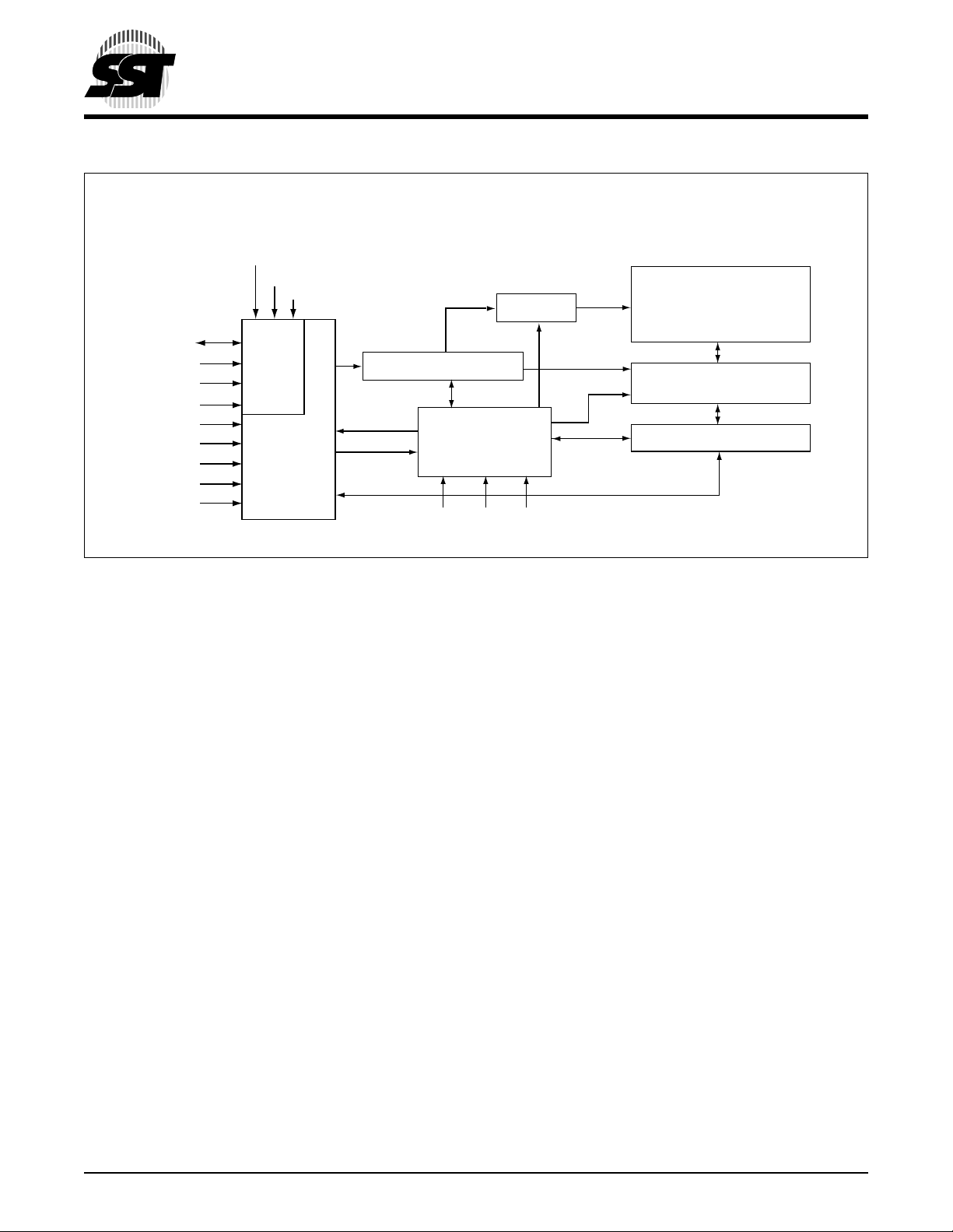
FUNCTIONAL BLOCK DIAGRAM
TBL#
WP#
INIT#
X-Decoder
2 Megabit LPC Flash
SST49LF020
Advance Information
SuperFlash
Memory
LAD[3:0]
LCLK
LFRAME#
GPI[4:0]
R/C#
A[10:0]
DQ[7:0]
OE#
WE#
LPC
Interface
Programmer
Interface
Address Buffers & Latches
Control Logic
RST#
Y-Decoder
I/O Buffers and Data Latches
CE#MODE
526 ILL B1.1
©2001 Silicon Storage Technology, Inc. S71175-02-000 5/01 526
6
2 Megabit LPC Flash
SST49LF020
Advance Information
TBL#
WP# for
Block 0~14
Block 15
Block 14
Block 13
Block 12
Block 11
Block 10
Block 9
Block 8
Block 7
Block 6
Block 5
Block 4
Block 3
Block 2
Block 1
Block 0
(16 KByte)
3FFFFH
3C000H
3BFFFH
38000H
37FFFH
34000H
33FFFH
30000H
2FFFFH
2C000H
2BFFFH
28000H
27FFFH
24000H
23FFFH
20000H
1FFFFH
1C000H
1BFFFH
18000H
17FFFH
14000H
13FFFH
10000H
0FFFFH
0C000H
0BFFFH
08000H
07FFFH
04000H
03FFFH
300000
02FFFH
02000H
01FFFH
01000H
00FFFH
00000H
Boot Block
4 KByte Sector 3
4 KByte Sector 2
4 KByte Sector 1
4 KByte Sector 0
526 ILL F52.3
DEVICE MEMORY MAP FOR SST49LF02 0
©2001 Silicon Storage Technology, Inc. S71175-02-000 5/01 526
7
2 Megabit LPC Flash
SST49LF020
Advance Information
NC
NC
NC
NC (CE#)
MODE (MODE)
A10 (GPI4)
R/C# (LCLK)
V
DD (VDD
NC
RST# (RST#)
A9 (GPI3)
A8 (GPI2)
A7 (GPI1)
A6 (GPI0)
A5 (WP#)
A4 (TBL#)
1
2
3
4
5
6
7
)
8
9
10
11
12
13
14
15
16
Standard Pinout
T op Vie w
Die Up
( ) Designates LPC Mode
FIGURE 1: PIN ASSIGNMENTS FOR 32-LE A D TSOP (8MM X 14MM)
)
DD
(V
DD
R/C# (LCLK)
A8 (GPI2)
A9 (GPI3)
RST# (RST#)NCV
A10 (GPI4)
32
31
30
29
28
27
26
25
24
23
22
21
20
19
18
17
OE# (INIT#)
WE# (LFRAME#)
VDD (VDD)
DQ7 (RES)
DQ6 (RES)
DQ5 (RES)
DQ4 (RES)
DQ3 (LAD3)
V
SS (VSS
DQ2 (LAD2)
DQ1 (LAD1)
DQ0 (LAD0)
A0 (RES)
A1 (RES)
A2 (RES)
A3 (RES)
526 ILL F01.2
)
FIGURE 2: P
4 3 2 1 32 31 30
A7(GPI1)
A6 (GPI0)
A5 (WP#)
A4 (TBL#)
A3 (RES)
A2 (RES)
A1 (RES)
A0 (RES)
DQ0 (LAD0)
5
6
7
8
32-lead PLCC
9
10
T op Vie w
11
12
13
14 15 16 17 18 19 20
DQ1 (LAD1)
DQ2 (LAD2)
( ) Designates LPC Mode
IN ASSIGNMENTS FOR 32-LEAD PLCC
)
SS
(V
SS
V
DQ3 (LAD3)
DQ4 (RES)
DQ5 (RES)
29
MODE (MODE)
28
NC (CE#)
27
NC
26
NC
25
VDD (VDD)
24
OE# (INIT#)
23
WE# (LFRAME#)
NC
22
DQ7 (RES)
21
DQ6 (RES)
526 ILL F02.2
©2001 Silicon Storage Technology, Inc. S71175-02-000 5/01 526
8
2 Megabit LPC Flash
SST49LF020
Advance Information
TABLE 2: PIN DESCRIPTION
Interface
Symbol Pin Name Type
A
10-A0
-DQ0Data I/O X To output data during Read cycles and receive input data during Write cycles.
DQ
7
Address I X Inputs for low-order addresses during Read and Write operations. Addresses
OE# Output Enable I X To gate the data output buffers.
WE# Write Enable I X To control the Write operations.
MODE Interface
Mode Select
INIT# Initialize I X This is the second reset pin for in-system use. This pin is internally combined
GPI[4:0] General
Purpose Inputs
TBL# T op Block Lock I X When low, prevents programming boot block sectors at top of memory. When
LAD[3:0] Address and
Data
LCLK Clock I X T o provide a clock input to the control unit
LFRAME# Frame I X To indicate start of a data tr an sf er opera tion; also used t o a bort an LPC cy cle
RST# Reset I X X To reset the operation of the device
WP# Write Protect I X When low, pre v ents programming to all but the highest addressable top boot
R/C# Row/Column
Select
RES Reserved X These pins must be left unconnected.
V
DD
Power Supply I X X To provide power supply (3.0-3.6V)
Vss Ground I X X Circuit ground (OV reference)
CE# Chip Enable I X This signal must b e a s se rted to se lect the device. Wh en C E# is low, the d evice
NC No Connection I X X Unconnected pins.
1. I=Input, O=Output
1
FunctionsPP LPC
are internally latched during a Write cycle. For the programming interface, these
addresses are latched by R/C# and share the same pins as the high-order
address inputs.
Data is internally latched during a Write cycle. The outputs are in tri-state when
OE# is high.
I X X This pin determines which interf a ce is opera tiona l. When hel d high, prog ram mer
mode is enabled and w hen held low, LPC mode is enabled. This pin mus t be
setup at power-up or befo re return from reset and not change during de vice operation. This pin is internally pulled do wn with a resistor b etwe en 20-100KΩ.
with the RST# pin; If this pin or RST# pin is driven low, identical operation is
exhibited.
I X These individual inputs can be used for additional board flexibility. The state of
these pins can be read through LPC registers. These inputs should be at their
desired state before the start of the PCI clock cycle during which the read is
attempted, and should remain in place until the end of the Read cycle. Unused
GPI pins must not be floated.
TBL# is high it disables hardware write protection for the top block sectors.
I/O X To provide LPC control signals, as well as addresses and Command
Inputs/Outputs data.
in progress.
blocks. When WP# is high it disables hardware write protection for these b locks.
I X Select for the Programming interface, this pin determines whether the address
pins are pointing to the row addresses, or to the column addresses.
is enabled. When CE# is high, the device is placed in low power standby mode.
T2.3 526
©2001 Silicon Storage Technology, Inc. S71175-02-000 5/01 526
9
2 Megabit LPC Flash
SST49LF020
Advance Information
TABLE 3: OPERATION MODES SELECTION (PP MODE)
Mode RST# OE# WE# DQ Address
Read
Program V
Erase V
Reset V
Write Inhibit
V
IH
IH
IH
IL
V
IH
X
Product Identification V
1. X can be VIL or VIH, but no other value.
2. Device ID = 61H
IH
TABLE 4: SOFTWARE COMMAND SEQUENCE
1
1st
Command Sequence
Byte-Program 5555H AAH 2AAAH 55H 5555H A0H BA
Sector-Erase 5555H AAH 2AAAH 55H 5555H 80H 5555H AAH 2AAAH 55H SAx
Block-Erase 5555H AAH 2AAAH 55H 5555H 80H 5555H AAH 2AAAH 55H BAx
Chip-Erase
Software ID Entry
Software ID Exit
Software ID Exit
1. LPC Mode use consecutive Write cycles to complete a command sequence;
2. Address format A14-A0 (Hex), Addresses A15-A21 can be VIL or VIH, but no other value, for the Command sequence in PP Mode.
3. BA = Program Byte address
4. SAx for Sector-Erase Address
5. BAx for Block-Erase Address
6. Chip-Erase is supported in PP Mode only
7. With A17-A1=0;SST Manufacturer’s ID=BFH, is read with A0=0.
8. Both Software ID Exit operations are equivalent
6
7
8
8
PP Mode use consecutive bus cycles to complete a command sequence.
SST49LF020 Device ID = 61H, is read with A
Write Cycle
2
Addr
Data Addr2Data Addr2Data Addr2Data Addr2Data Addr2Data
5555H AAH 2AAAH 55H 5555H 80H 5555H AAH 2AAAH 55H 5555H 10H
5555H AAH 2AAAH 55H 5555H 90H
XXH F0H
5555H AAH 2AAAH 55H 5555H F0H
V
IL
V
IH
V
IH
V
IL
V
IL
V
IL
D
D
X
OUT
IN
1
A
IN
A
IN
Sector or Block address,
XXH for Chip-Erase
XXHigh Z X
V
IL
V
IH
V
IL
1
2nd
Write Cycle
V
IL
X
V
IL
3rd
Write Cycle
=1.
0
High Z/D
High Z/D
OUT
OUT
Manufacturer’s ID (BFH)
Device ID
1
2
1
4th
Write Cycle
3
Data
X
X
A18-A1=VIL, A0=V
A18-A1=VIL, A0=V
1
5th
Write Cycle
Write Cycle
IL
IH
6th
4
5
T3.2 526
1
30H
50H
T4.5 526
©2001 Silicon Storage Technology, Inc. S71175-02-000 5/01 526
10
2 Megabit LPC Flash
SST49LF020
Advance Information
Absolute Maximum Stress Ratings (Applied conditions greater than those listed under “Absolute Maximum
Stress Ratings” may cause pe r manent dama ge to the device. This is a stres s rating only and funct ional operatio n
of the device at these conditions or conditions greater tha n those defined in the ope rational sections of this data
sheet is not implied. Exposure to absolute maximum stress rating conditions may affect device reliability.)
Temperature Under Bias . . . . . . . . . . . . . . . . . . . . . . . . . . . . . . . . . . . . . . . . . . . . . . . . . . . . . . . . . -55°C to +125°C
Storage Temperature . . . . . . . . . . . . . . . . . . . . . . . . . . . . . . . . . . . . . . . . . . . . . . . . . . . . . . . . . . . -65°C to +150°C
D. C. Voltage on Any Pin to Ground Potential . . . . . . . . . . . . . . . . . . . . . . . . . . . . . . . . . . . . . . . -0.5V to
Transient Voltage (<20 ns) on Any Pin to Ground Potential . . . . . . . . . . . . . . . . . . . . . . . . . . . . -1.0V to
Package Power Dissipation Capability (Ta=25°C) . . . . . . . . . . . . . . . . . . . . . . . . . . . . . . . . . . . . . . . . . . . . . . . 1.0W
Surface Mount Lead Soldering Temperature (3 Seconds) . . . . . . . . . . . . . . . . . . . . . . . . . . . . . . . . . . . . . . . 240°C
1
Output Short Circ uit Curr ent
1. Outputs shorted for no more than one second. No more than one output shorted at a time.
. . . . . . . . . . . . . . . . . . . . . . . . . . . . . . . . . . . . . . . . . . . . . . . . . . . . . . . . . . . . . 50 mA
V
DD
V
DD
+ 0.5V
+ 1.0V
OPERATING RANGE
Range Ambient Temp V
Commercial 0°C to +85°C 3.0-3.6V
DD
AC CONDITIONS OF TEST
Input Rise/Fall Time . . . . . . . . . . . . . . . 3 ns
Output Load . . . . . . . . . . . . . . . . . . . . . C
See Figures 25 and 26
1. LPC interface signals use PCI load condition.
TABLE 5: DC OPERATING CHARACTERISTICS (ALL INTERFACES)
Limits
Symbol Parameter
I
DD
I
SB
1
I
RY
I
I
I
LI
I
LO
V
IHI
V
ILI
V
IL
V
IH
V
OL
V
OH
1. The device is in Ready Mode when no activity is on the LPC bus.
Power Supply Current Address input=VIL/VIH, at f=1/TRC Min,
Read 12 mA OE#=VIH, WE#=V
Write 24 mA OE#=VIH, WE#=VIL, VDD=VDD Max (PP Mode)
Standby VDD Current
100 µA LFRAME#=VIH, f=33 MHz, CE#=V
(LPC Interface)
Ready Mode VDD Current
10 mA LFRAME#=VIL, f=33 MHz, VDD=VDD Max
(LPC Interface)
Input Current for IC Pin 200 µA VIN=GND to VDD, VDD=VDD Max
Input Leakage Current 1 µA VIN=GND to VDD, VDD=VDD Max
Output Leakage Current 1 µA V
INIT# Input High Voltage 1.0 VDD+0.5 V VDD=VDD Max
INIT# Input Low Voltage -0.5 0.4 V VDD=VDD Max
Input Low Voltage -0.5 0.3 V
Input High Voltage 0.5 V
DDVDD
Output Low Voltage 0.1 V
Output High Voltage 0.9 V
DD
DD
+0.5 V VDD=VDD Max
DD
VVDD=VDD Min
VIOL=1500 µA, VDD=VDD Min
VIOH=-500 µA, VDD=VDD Min
1
Test Condit ionsMin Max Units
V
DD=VDD
Max (PP Mode)
IH
VDD=VDD Max,
All other inputs ≥ 0.9 V
All other inputs ≥ 0.9 V
=GND to VDD, VDD=VDD Max
OUT
or ≤ 0.1 V
DD
or ≤ 0.1 V
DD
= 30 pF
L
IH
DD
DD
T5.5 526
©2001 Silicon Storage Technology, Inc. S71175-02-000 5/01 526
11
2 Megabit LPC Flash
SST49LF020
Advance Information
TABLE 6: RECOMMENDED SYSTEM POWER-UP TIMINGS
Symbol Parameter Minimum Units
T
PU-READ
T
PU-WRITE
1
1
1. This parameter is measured only for initial qualification and after a design or process change that could affect this parameter
Power-up to Read Operation 100 µs
Power-up to Write Operation 100 µs
T6.1 526
TABLE 7: PIN CAPACITANCE (V
=3.3V, Ta=25 °C, f=1 Mhz, other pins open)
DD
Parameter Description Test Condition Maximum
1
C
I/O
1
C
IN
2
L
PIN
1. This parameter is measured only for initial qualification and after a design or process change that could affect this parameter.
2. Refer to PCI Spec.
I/O Pin Capacitance V
=0V 12 pF
I/O
Input Capacitance VIN=0V 6 pF
Pin Inductance 20 nH
TABLE 8: RELIABILITY CHARACTERISTICS
Minimum
Symbol Parameter
1
N
END
1
T
DR
1
I
LTH
1. This parameter is measured only for initial qualification and after a design or process change that could affect this parameter.
Endurance 10,00 0 Cycles JEDEC Standard A117
Data Retention 100 Years JEDEC Standard A103
Latch Up 100 + I
Specification Units Test Method
DD
mA JEDEC Standard 78
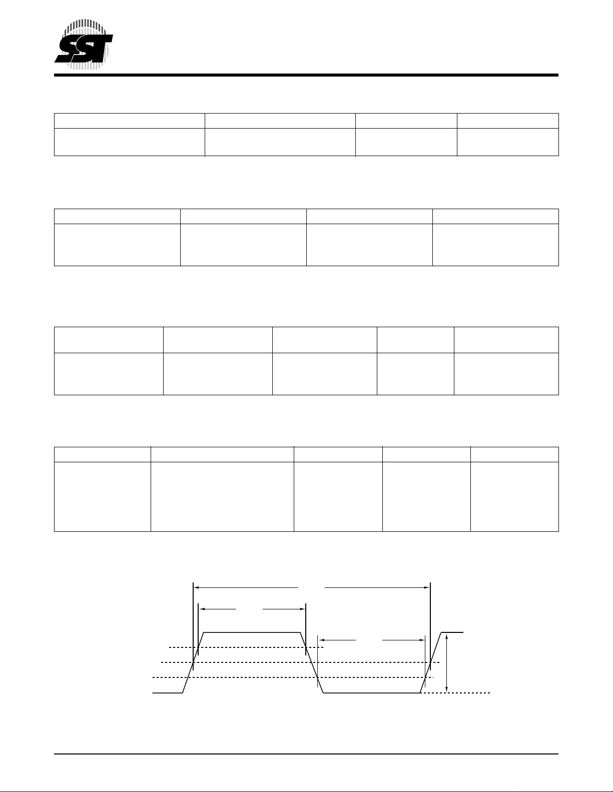
TABLE 9: CLOCK TIMING PARAMETERS (LPC MODE)
Symbol Parameter Min Max Units
T
CYC
T
HIGH
T
LOW
- LCLK Slew Rate (peak-to-peak) 1 4 V/ns
- RST# or INIT# Slew Rate 50 mV/ns
LCLK Cycle Time 30 ns
LCLK High T i me 11 ns
LCLK Low Time 11 ns
T7.0 526
T8.1 526
T9.0 526
T
cyc
T
high
0.6 V
0.4 V
0.3 V
0.5 V
DD
DD
DD
DD
T
low
0.2 V
DD
0.4 V
DD
(minimum)
526 ILL F27.0
p-to-p
FIGURE 3: LCLK WAVEFORM
©2001 Silicon Storage Technology, Inc. S71175-02-000 5/01 526
12
 Loading...