

Silicon Storage Technology Inc SST49LF008A-33-4C-WH, SST49LF008A-33-4C-NH, SST49LF004A-33-4C-WH, SST49LF004A-33-4C-NH, SST49LF003A-33-4C-WH Datasheet
...
2 Mbit / 3 Mbit / 4 Mbit / 8 Mbit Firmware Hub
SST49LF002A / SST49LF003A / SST49LF004A / SST49LF008A
SST49LF002A / 003A / 004A / 008A2 Mb / 3 Mb / 4 Mb / 8 Mb Firmware Hub for Intel 8xx Chipsets
FEATURES:
Advance Information
• Firmware Hub for Intel 8xx Chipsets
• 2 Mbit, 3 Mbit, 4 Mbit, or 8 Mbit SuperFlash
memory array for code/data storage
– SST49LF002A: 256K x8 (2 Mbit)
– SST49LF003A: 384K x8 (3 Mbit)
– SST49LF004A: 512K x8 (4 Mbit)
– SST49LF008A: 1024K x8 (8 Mbit)
• Flexible Erase Capability
– Uniform 4 KByte Sectors
– Uniform 16 KByte overlay blocks for
SST49LF002A
– Uniform 64 KByte overlay blocks for
SST49LF003A/004A/008A
– Top Boot Block protection
- 16 KByte for SST49LF002A
- 64 KByte for SST49LF003A/004A/008A
– Chip-Erase for PP Mode Only
• Single 3.0-3.6V Read and Write Operations
• Superior Reliability
– Endurance:100,000 Cycles (typical)
– Greater than 100 years Data Retention
• Low Power Consumption
– Active Read Current: 6 mA (typical)
– Standby Current: 10 µA (typical)
• Fast Sector-Erase/Byte-Program Operation
– Sector-Erase Time: 18 ms (typical)
– Block-Erase Time: 18 ms (typical)
– Chip-Erase Time: 70 ms (typical)
– Byte-Program Time: 14 µs (typical)
– Chip Rewrite Time:
SST49LF002A: 4 seconds (typical)
SST49LF003A: 6 seconds (typical)
SST49LF004A: 8 seconds (typical)
SST49LF008A: 15 seconds (typical)
– Single-pulse Program or Erase
– Internal timing generation
• Two Operational Modes
– Firmware Hub Interface (FWH) Mode for
in-system operation
– Parallel Programming (PP) Mode for fast
production programming
• Firmware Hub Hardware Interface Mode
– 5-signal communication interface supporting
byte Read and Write
– 33 MHz clock frequency operation
– WP# and TBL# pins provide hardware write
protect for entire chip and/or top Boot Block
– Block Locking Register for all blocks
– Standard SDP Command Set
– Data# Polling and Toggle Bit for End-of-Write
detection
– 5 GPI pins for system design flexibility
– 4 ID pins for multi-chip selection
• Parallel Programming (PP) Mode
– 11-pin multiplexed address and
8-pin data I/O interface
– Supports fast In-System or PROM programming
for manufacturing
• CMOS and PCI I/O Compatibility
• Packages Ava ilable
– 32-lead PLCC
– 32-lead TSOP (8mm x 14mm)
PRODUCT DESCRIPTION
The SST49LF00xA flash memory devices are designed
to be read-compat ib le with t he Int el 8280 2 Firmware Hub
(FWH) device for PC-BIOS application. It provides protection for the storage and update of code and data in
addition to adding system design flexibility through five
general purpose inputs. Two interface modes are supported by the SST49LF00xA: Firmware Hub (FWH)
Interface Mode for In-System programming and Parallel
Programming (PP) Mode for fast factory programming of
PC-BIOS applications.
©2001 Silicon Storage Technology, Inc.
S71161-06-000 9/01 504
1
MPF is a trademark of Silicon Storage Technology, Inc. Intel is a registered trademark of Intel Corporation.
The SST49LF00xA flash memory devices are manufactured with SST’s proprietary, high performance SuperFlash Technology. The split-gate cell design and thick
oxide tunneling injector attain better reliability and manufacturability compared with alternate approaches. The
SST49LF00xA devices significantly improve perfor mance
and reliability, while lowering power consumption. The
SST49LF00xA devices write (Program or Erase) with a
single 3.0-3.6V power supply. It uses less energy during
Erase and Program than alternative flash memory technologies. The total energy consumed is a function of the
applied voltage, current and time of application. Since for
The SST logo and SuperFlash are registered trademarks of Silicon Storage Technology, Inc.
These specifications are subject to change without notice.

2 Mbit / 3 Mbit / 4 Mbit / 8 Mbit Firmware Hub
SST49LF002A / SST49LF003A / SST49LF004A / SST49LF008A
Advance Information
any given voltage range, the SuperFlash technology uses
less current to program and has a shorter erase time, the
total energy consumed during any Erase or Program operation is less than alternative flash memory technologies.
The SST49LF00xA products provide a maximum ByteProgram time of 20 µsec. The entire memory can be
erased and programmed byte-by-byte typically in 15 seconds for an 8-Mbit device, when using status detection
features such as Toggle Bit or Data# Polling to indicate the
completion of Program operation. The SuperFlash technology provides fixed Erase and Program time, independent of the number of Erase/Program cycles that have
performed. Therefore the system software or hardware
does not have to be calibrated or correlated to the cumulated number of Erase/Program cycles as is necessary
with alternative flash memory technologies, whose Erase
and Program time increase with accumulated Erase/Program cycles.
To protect against inadvertent write, the SST49LF00xA
devices employ hardware and software data (SDP) protection schemes. It is offered with typical endurance of
100,000 cycles. Data retention is rated at greater than 100
years.
To meet high density, surface mount requirements, the
SST49LF00xA device is offered in 32- lead T SOP and 32lead PLCC packages. See Figures 7 and 8 for pinouts and
Table 8 for pin descriptions.
Mode Selection and Description
The SST49LF00xA flash memory de vices can ope r ate in
two distinct interface modes: the Firmware Hub Interface
(FWH) mode and the Parallel Programming (PP) mode.
The IC (Interface Configuration pin) is used to set the
interface mo de selection . I f the I C pin is set to lo gic H igh ,
the device is in PP mode; while if the IC pin is set Low,
the device is in the FWH mode . The IC selection pin mu st
be configured prior to device operation. The IC pin is
internally pulled do wn if t he p in is not co nne cte d. I n FWH
mode, the device is configured to interface with its host
using Intel’ s Fi rmware Hub pr oprietary protocol. Comm u-
nication between H ost a nd the SS T4 9LF0 0xA occu rs via
the 4-bit I/O communication signals, FWH [3:0] and the
FWH4. In PP mode , the de vice is p rogr ammed via an 1 1bit address and an 8-bit data I/O parallel signals. The
address inputs are multiplexed in row and column
selected by control signal R/C# pin. The column
addresses are mapped to the higher internal addresses,
and the row addresses are mapped to the lower internal
addresses. See the Device Memory Maps in Figures 3
through 6 for add ress assignmen ts .
FIRMWARE HUB (FWH) MODE
Device Operation
The FWH mode uses a 5-s ignal com munication inte rface,
FWH[3:0] and FWH4, to control operations of the
SST49LF00xA. Operations such as Memory Read and
Memory Write uses Intel FWH propriety protocol. JEDEC
Standard SDP (Software Data Protection) Byte-Program,
Sector-Erase and Block-Erase command sequences are
incorp orated into the FWH memor y cycles. Chip -Erase is
only available in PP Mode.
The device enters standby mode when FWH4 is high and
no internal operation is in progress. The device is in ready
mode when FWH4 is low and no activity is on the FWH b us.
Firmware Hub Interface Cycles
Addresses and data are transferred to and from the
SST49LF00xA by a series of “fields,” where each field contains 4 bits of data. ST49LF00xA supports only single-byte
read and writes, and all fields are one clock cycle in length.
Field sequences and contents are strictly defined for Read
and Write operations. Addresses in this section refer to
addresses as seen from the SST49LF00xA’s “point of
view,” some calculation will be required to translate these to
the actual locati on s in the memory ma p ( a nd vi c e versa) i f
multiple memory device is used on the bus. T ables 1 and 2
list the fiel d seque nces f or Re ad and Wri te cycle s.
©2001 Silicon Storage Technology, Inc. S71161-06-000 9/01 504
2
2 Mbit / 3 Mbit / 4 Mbit / 8 Mbit Firmware Hub
SST49LF002A / SST49LF003A / SST49LF004A / SST49LF008A
Advance Information
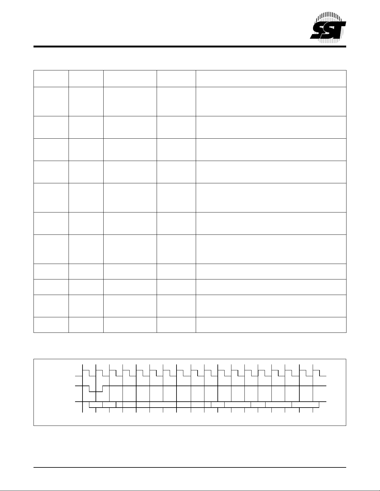
TABLE 1: FWH READ CYCLE
Clock
Cycle
1 START 1101 IN FWH4 must be acti v e (lo w) for the part to respond. Only the
2 IDSEL 0000 to 1111 IN Indicates which FWH device should respond. If the to IDSEL (ID
3-9 IMADDR YYYY IN These seven clock cycles make up the 28-bit memory
10 IMSIZE 0000 (1 byte) IN A field of this size indica tes ho w man y b ytes will be or tra ns-
11 TAR0 1111 IN
12 TAR1 1111 (float) Float
13 RSYNC 0000 (READY) OUT During this clock cycle, the FWH will generate a “ready-
14 DATA YYYY OUT YYYY is the least-significant nibble of the least-significant
15 DATA YYYY OUT YYYY is the most-significant nibble of the least-significant
16 TAR0 1111 OUT
17 TAR1 1111 (float) Float thenINThe master (Intel ICH) resumes control of the bus during
1. Field contents are valid on the rising edge of the present clock cycle.
Field
Name
Field Contents
FWH[3:0]
1
FWH[3:0]
Direction Comments
last start field (before FWH4 transitioning high) should be
recognized. The START field contents indicate a FWH
memory read cycle.
select) field matches the value ID[3:0], then that particular device
will respond to the whole bus cycle.
address. YYYY is one nibble of the entire address.
Addresses are transferred most-significant nibble first.
ferred during multi-byte operations. The SST49LF00xA will
only support single-byte operation. IMSIZE=0000b
In this clock cy cle , the m aster (In tel IC H) has driven the bus
then Float
then float to all ‘1’s and then floats the bus, prior to the next
clock cycle. This is the first part of the bus “turnaround
cycle.”
The SST49LF00xA takes control of the bus during this
then OUT
cycle. Durin g the next clock cycle, it will be driving “sync
data.”
sync” (RSYNC) indicating that the least-sig nifica nt nib ble of
the least-significant byte will be available during the next
clock cycle.
data byte.
data byte.
In this clock cycle, the SST49LF00xA has driven the bus to
then Float
all ones and th en flo ats th e b us prior to the n e xt c loc k cycl e.
This is the first part of the bus “turnaround cycle.”
this cycle.
T1.3 504
CLK
FWH4
FWH[3:0]
STR TAR RSYNCIMSIMADDRIDS DATA TAR
504 ILL F59.1
FIGURE 1: SINGLE-BYTE READ WAVEFORMS
©2001 Silicon Storage Technology, Inc. S71161-06-000 9/01 504
3
2 Mbit / 3 Mbit / 4 Mbit / 8 Mbit Firmware Hub
SST49LF002A / SST49LF003A / SST49LF004A / SST49LF008A
Advance Information
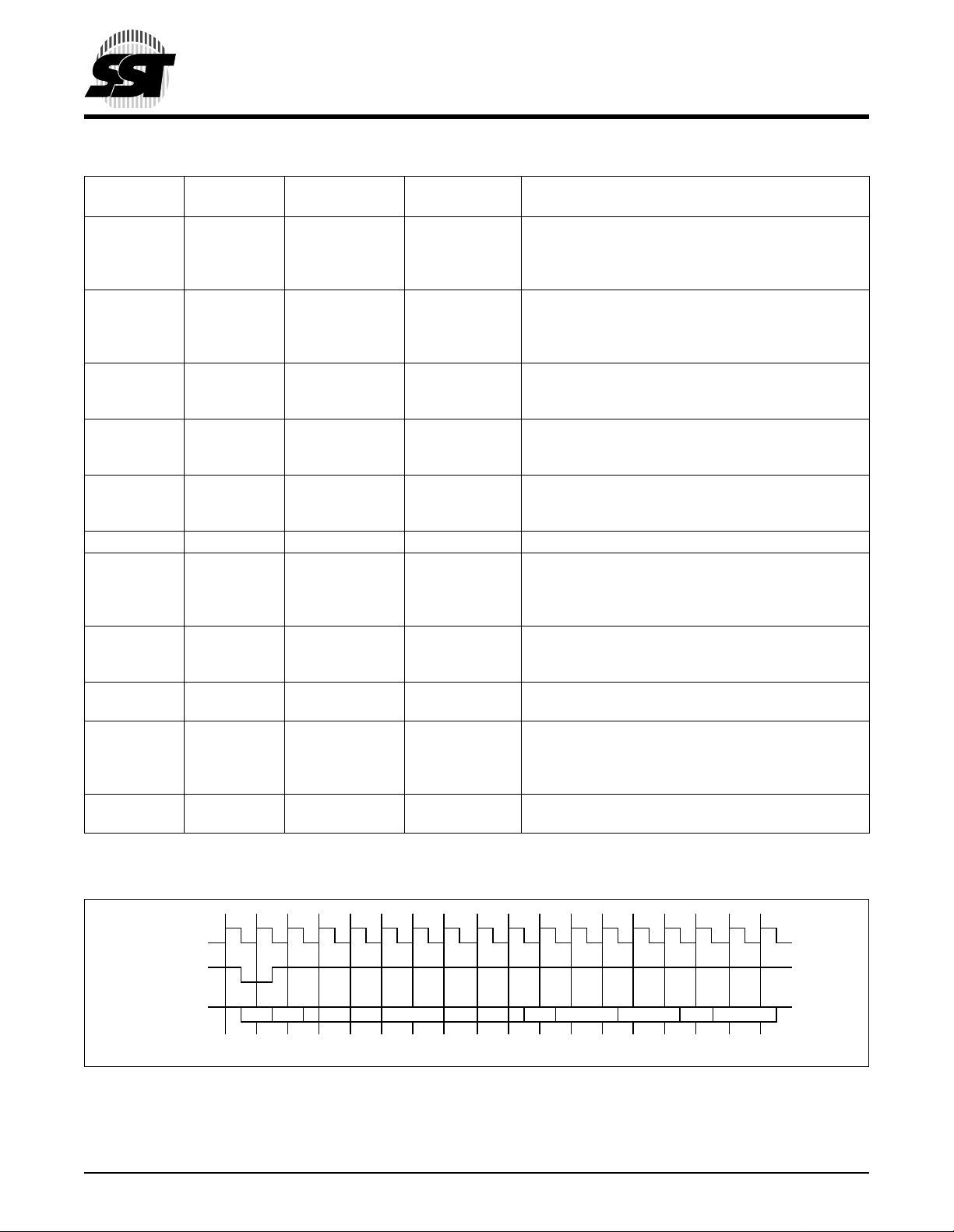
TABLE 2: FWH WRITE CYCLE
Clock
Cycle
1 START 1110 IN FWH4 must be active (low) for the part to respond.
2 IDSEL 0000 to 1111 IN Indicates which SST49LF00xA device should
3-9 IMADDR YYYY IN These seven clock cycles make up the 28-bit memory
10 IMSIZE 0000 (1 byte) IN This size field indicates how many bytes will be
11 DATA YYYY IN This field is the lea st-signif icant n ibb le of the d ata b yte .
12 DATA YYYY IN This field is the most-significant nibble of the data b y te.
13 TAR0 1111 IN then Float In this clock cycle, the master (Intel ICH) has driven the
14 TAR1 1111 (float) Float then OUT T he SST49LF00xA takes control of the bus during this
15 RSYNC 0000 OUT The SST49LF00xA outputs the values 0000, indicat-
16 TAR0 1111 OUT then Float In this clock cycle, the SST49LF00xA has driven the
17 TAR1 1111 (float) Float then IN The master (Intel ICH) resumes control of the bus during
1. Field contents are valid on the rising edge of the present clock cycle.
Field
Name
Field Contents
FWH[3:0]
1
FWH[3:0]
Direction Comments
Only the last start field (before FWH4 transitioning
high) should be recognized. The START field contents
indicate a FWH memory read cycle.
respond. If the IDSEL (ID select) f ield matches the
value ID[3:0], then that particular device will respond
to the whole bus cycle.
address. YYYY is one nibble of the entire address.
Addresses are transferred most-significant nibble first.
transferred during multi-byte operations. The FWH
only supports single-byte wr ites. I MSIZE=0 000b
This data is either the data to be programmed into the
flash memory or any valid flash command.
then float bus to all ‘1’s and then floats the bus prior to
the next clock cycle. This is the first part of the bus
“turnaround cycle.”
cycle. During the next clock cycle it will be driving the
“sync” data.
ing that it h as received data or a flash command.
bus to all then float ‘1’s and then floats the bus prior to
the next clock cycle. This is the first part of the bus
“turnaround cycle.”
this cycle.
T2.4 504
CLK
FWH4
FWH[3:0]
STR DATA TARTAR
IMSIMADDRIDS
RSYNC
504 ILL F60.1
FIGURE 2: WRITE WAVEFORMS
©2001 Silicon Storage Technology, Inc. S71161-06-000 9/01 504
4

2 Mbit / 3 Mbit / 4 Mbit / 8 Mbit Firmware Hub
SST49LF002A / SST49LF003A / SST49LF004A / SST49LF008A
Advance Information
Abort Mechanism
If FWH4 is driven low for one or more clock cycles during a
FWH cycle, the cycle will be terminated and the device will
wait for the ABORT command. The ho st must drive the
FWH[3:0] with ‘1111b’ (ABORT command) to return the
device to ready mode. If abor t occurs during the inte rnal
write cycle, the data may be incorrectly programmed or
erased. It is required to wait for the Write operation to complete prior to initiation of the abort com mand. It is recommended to check the Write status with Data# Polling (DQ
or Toggle Bit (DQ
) pins. One other option is to wait for the
6
fixed write time to expire.
Response To Invalid Fields
During FWH opera tions, the FWH will not exp licit ly in dica te
that it has received invalid field sequ ences. The respon se
to specific invalid fields or sequences is as follows:
Address out of range: The FWH address s equence is
7 fields long (28 bi ts), but only the last five addre ss fields
(20 bits) will be decoded by SST49LF00xA.
Address A
writes to the flash core (A
=0).
(A
22
has the special f unction of dire cting re ads and
22
=1) or to the register space
22
The SST49LF003A features are equivalent to the
SST49LF004A with 128 KByte less memory. For the
SST49LF003A, operations beyond the 3-Mbit boundary (below 20000H) are not valid (see Device Memo ry
Map). Invalid address range locations will read as
00H.
Invalid IMSIZE field: If the FWH receives a n in v a lid s ize
field during a Read or Write operation, the device will reset
and no operation will be attempted. The SST49LF00xA will
not generate any kind of r e sp on se in this situat io n. Invalidsize fields for a Read/Write cycle are anything but 0000b.
Once valid START , IDSEL, and IMSIZE fields are received,
the SST49LF00xA always will respond to subsequent
inputs as if they were valid. As long as the states of device
FWH[3:0] and FWH4 are known, the response of the
SST49LF00xA to sig nals received during the FWH cycle
should be predic table. The S ST4 9LF0 0xA will make no
attempt to check the validity of incoming flash operation
commands.
Device Memory Hardware Write Protection
The Top Boot Lock (TBL#) and Write Protect (WP#) pins
are provided for hardware write protection of device
memory in the SST49LF00xA. The TBL# pin is used to
write protect 16 boot sectors (64 KByte) at the highest
flash memory address range for the SST49LF003A/
004A/008A and 4 boot sectors (16 KByte) for
SST49LF002A. WP# pin write protects the remaining
sectors in the flash memory.
An active low signal at the TBL# pin prevents Program and
Erase operations of the top boot sectors. When TBL# pin is
held high, write protection of the top boot sectors is then
determin ed by the Boot Block Lockin g register. The WP#
pin serves the same fu nction for the remainin g sectors of
)
7
the device memory. The TBL# and WP# pins write protection functions operate independently of one another.
Both TBL# and WP# p ins must be set to their require d
protection states prior to starting a Program or Erase
operation. A logic level change occurring at the TBL# or
WP# pin during a Program or Erase operation could
cause unpredictable res ults. TBL# and WP# pins cann ot
be left unconnected.
TBL# is inter nally ORed with th e top Boot Block Locking
register. When TBL# is low, the top Boot Block is hardware write protected regardles s of the sta te of the Wr iteLock bit for the Boot Block Locking register. Clearing the
Write-Protect bit in the register when TBL# is low will have
no functional effect, even though the register may indicate
that the block is no longer locked.
WP# is internal ly ORed with the Block Locking register.
When WP# is low, the blocks are hardware write protected regardless of the stat e of th e W r ite- Lock bit for the
corresponding Block Locking registers. Clearing the
Write-Protect bit in any register when WP# is low will have
no functional effect, even though the register may indicate
that the block is no longer locked.
Reset
A VIL on INIT# or RST# pin initiates a device reset. INIT#
and RST# pins have the same function internally. It is
required to dri ve INIT# or RST# pins l ow during a sy stem
reset to ensure proper CPU initialization.
During a Read opera tion, driving IN IT# or RST# pins low
deselects the device and places the output drivers,
FWH[3:0], in a high-impedance state. The reset signal
must be held low for a minimal duration of ti me T
reset latency will occur if a reset procedure is performed
during a Program or Erase operation. See T ab le 18, Reset
Timing Parameters for more information. A device reset
during an active Program or E rase will abo rt the operatio n
and memory contents may become invalid due to data
being altered or corrupted from an incomplete Erase or
Program operation.
RSTP.
A
©2001 Silicon Storage Technology, Inc. S71161-06-000 9/01 504
5

2 Mbit / 3 Mbit / 4 Mbit / 8 Mbit Firmware Hub
SST49LF002A / SST49LF003A / SST49LF004A / SST49LF008A
Advance Information
Write Operation Status Detection
The SST49LF00xA device provides two software means to
detect the completion of a Write (Program or Erase) cycle,
in order to optimize the system write cycle time. The software detection includes two status bits: Data# Polling
) and Toggle Bit (DQ6). The End-of-Write detection
(DQ
7
mode is incorporated into the FWH Read Cycle. The actual
completion of the nonvolatile write is asynchronous with the
system; therefore, either a Data# Polling or Toggle Bit read
may be simultaneous with the completion of the Write
cycle. If thi s occurs, the system ma y possibl y get an errone ous result, i.e., valid data may appear to conflict with either
or DQ6. In order to prevent spurious reje ction, if an
DQ
7
erroneous result occurs, the software routine should
include a loop to read the acces sed lo cation an addit ional
two (2) times. If both read s are valid, then the device has
completed the Write cycl e, ot herwise the rejection is v alid.
Data# Polling (DQ7)
When the SST49LF00xA device is in the internal Program
operation, any attemp t to read DQ
will produce the com-
7
plement of the tru e data. Once the Program operation is
completed, DQ
though DQ
will produce true data. Note that even
7
may have valid data immediately following the
7
completion of an internal Write operation, the remaining
data outputs may still be invalid: valid data on the e ntire
data bus will appear in subsequent successive Read
cycles. During internal Erase operation, any attempt to
read DQ
tion is completed, DQ
will produce a ‘0’. Once the internal Erase opera-
7
will produc e a ‘1’. Proper status will
7
not be given using Data# Polling if the address is in the
inva lid r ange .
Toggle Bit (DQ6)
During the internal Program o r Era se oper ati on, an y consecutive attempts to read DQ
will produce alternating
6
‘0’s and ‘1’s, i.e., toggling between 0 and 1. When the
internal Program or Erase operation is completed, the
toggling will stop.
Multiple Device Selection
The four ID pins, ID[3:0], allow multiple devices to be
attached to the same bus by using different ID strapping in
a system. When the SST49LF00xA is used as a boot
device, ID[3:0] must be strapped as 0000, all subsequent
devices should use a sequential up-count strapping (i.e.
0001, 0010, 0011, etc.). T he SST49LF00xA will com pare
the strapping values, if there is a misma tch , the device will
ignore the remainder of the cycle and go into standby
mode. For further information regarding FWH device mapping and paging, p lease refer to the Intel 8280 1(ICH) I/O
Controller H ub documenta tion. Since there is no ID supp ort
in PP Mode, to program multiple devices a stand-alone
PROM programmer is recommended.
REGISTERS
There are three types of registers available on the
SST49LF00xA, the General Purpose Inputs Register,
Block Locking Registers and the JEDEC ID Registers.
These regist ers ap pea r at thei r res pect iv e a ddre ss loca tion
in the 4 GByte sys tem memo ry map. Unus ed regis ter lo cations will read as 00H. Any attempt to read or write any registers during internal Write operation will be ignored.
General Purpose Inputs Register
The GPI_REG (General P ur pose Inp uts Regist er) pass es
the state of FGPI[4:0] pins at power-up on the
SST49LF00xA. It is rec om me nd ed tha t th e FG PI[4 :0] pins
are in the desired state before FWH4 is brought low for the
beginning of the bus cycle, and remain in that state until the
end of the cycle. There is no default value since this is a
pass-through regi s ter. The GPI regis te r for the boot d evice
appears at FFBC0100 H in the 4 GByte system memory
map, an d will appea r else wher e if th e de vice is not th e boot
device. Register is not available for read when the device is
in Erase/Program operation. See Table 3 for the GPI_REG
bits and function.
TABLE 3: G
Bit Function
7:5 Reserved - -
4 FGPI[4]
Reads status of general
purpose input pin
3 FGPI[3]
Reads status of general
purpose input pin
2 FGPI[2]
Reads status of general
purpose input pin
1 FGPI[1]
Reads status of general
purpose input pin
0 FGPI[0]
Reads status of general
purpose input pin
ENERAL PURPOSE INPUTS REGISTER
Pin #
32-PLCC 32-TSOP
30 6
311
412
513
614
T3.2 504
©2001 Silicon Storage Technology, Inc. S71161-06-000 9/01 504
6
2 Mbit / 3 Mbit / 4 Mbit / 8 Mbit Firmware Hub
SST49LF002A / SST49LF003A / SST49LF004A / SST49LF008A
Advance Information
Block Locking Registers
SST49LF00xA provides so ftware controlled lock protection through a set of Blo ck Locking registers. The Block
Locking Registers are read/wr ite registers and it is accessible through st andard addressable memory locati ons
specified in Table 4 and Table 5. Unused register locations will read as 00H.
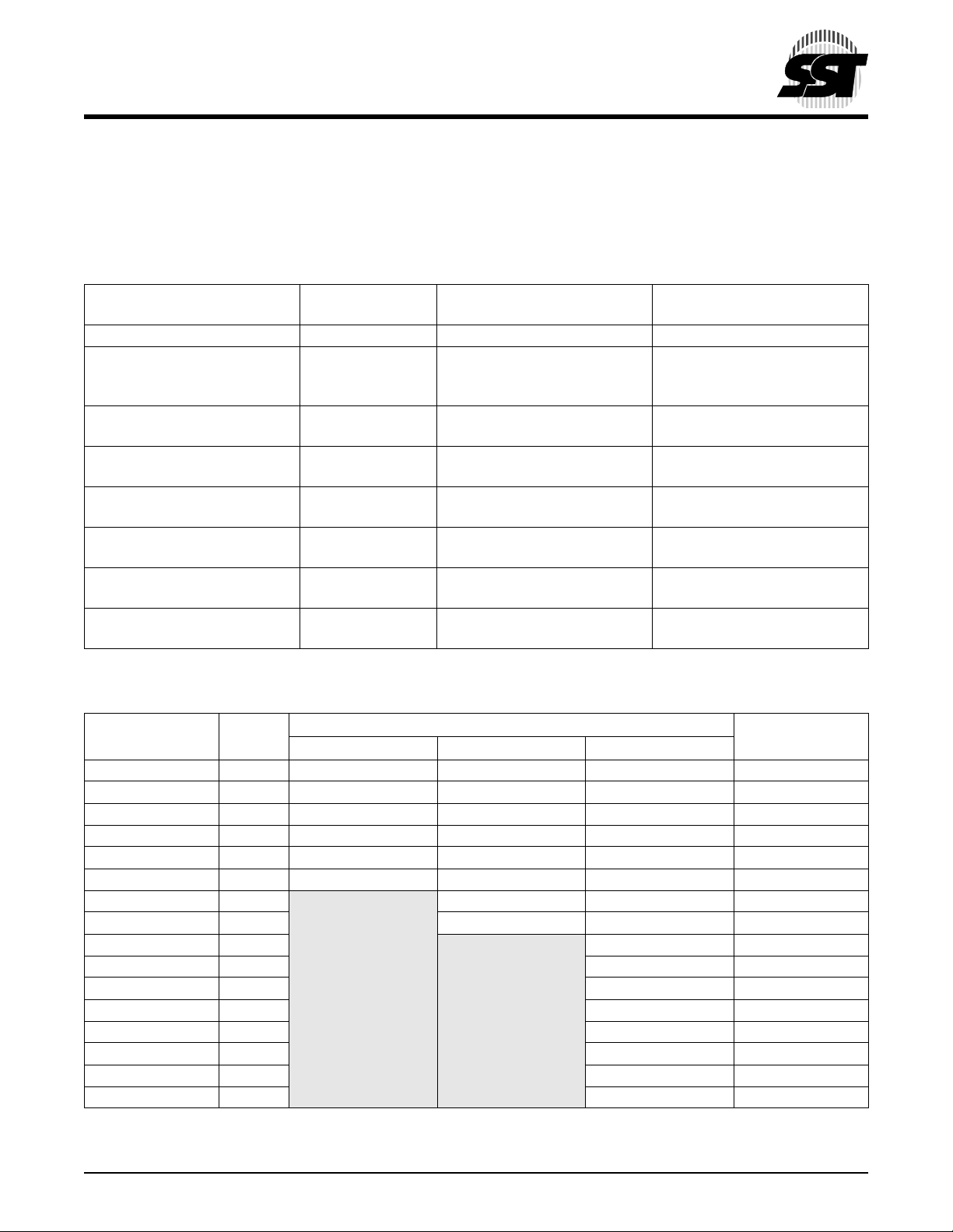
TABLE 4: B
Register Block Size
T_BLOCK_LK 16K 3FFFFH - 3C000H FFBF8002H
T_MINUS01_LK 16K
T_MINUS02_LK 16K
T_MINUS03_LK 16K
T_MINUS04_LK 16K
T_MINUS05_LK 16K
T_MINUS06_LK 16K
T_MINUS07_LK 16K
1. Default value at power up is 01H
LOCK LOCKING REGISTERS FOR SST49LF002A
16K
16K
16K
16K
16K
16K
16K
16K
TABLE 5: BLOCK LOCKING REGISTERS FOR SST49LF003A/004A/008A
Block
Register
T_BLOCK_LK 64K 07FFFFH - 070000H 07FFFFH - 070000H 0FFFFFH - 0F0000H FFBF0002H
T_MINUS01_LK 64K 06FFFFH - 060000H 0 6FF FFH - 060000H 0EFFFFH - 0E0000H FFBE0002H
T_MINUS02_LK 64K 05FFFFH - 050000H 05FFFFH - 050000H 0DFFFFH - 0D0000H FFBD0002H
T_MINUS03_LK 64K 04FFFFH - 040000H 04FFFFH - 040000H 0CFFFFH - 0C0000H FFBC0002H
T_MINUS04_LK 64K 03FFFFH - 030000H 0 3FF FFH - 030000H 0BFFFFH - 0B0000H FFBB0002H
T_MINUS05_LK 64K 02FFFFH - 020000H 0 2FF FFH - 020000H 0AFFFFH - 0A0000H FFBA0002H
T_MINUS06_LK 64K
T_MINUS07_LK 64K 00FFFFH - 000000H 08FFFFH - 080000H FFB80002H
T_MINUS08_LK 64K
T_MINUS09_LK 64K 06FFFFH - 060000H FFB60002H
T_MINUS10_LK 64K 05FFFFH - 050000H FFB50002H
T_MINUS11_LK 64K 04FFFFH - 040000H FFB40002H
T_MINUS12_LK 64K 03FFFFH - 030000H FFB30002H
T_MINUS13_LK 64K 02FFFFH - 020000H FFB20002H
T_MINUS14_LK 64K 01FFFFH -010000H FFB10002H
T_MINUS15_LK 64K 00FFFFH - 000000H FFB00002H
1. Default value at power up is 01H
Size
Protected Me mory Address Range
01FFFFH - 010000H 09FFFFH - 090000H FFB90002H
1
Protected Memory
Address Package
3BFFFH - 38000H
37FFFH - 34000H
33FFFH - 30000H
2FFFFH - 2C000H
2BFFFH - 28000H
27FFFH - 24000H
23FFFH - 20000H
1FFFFH - 1C000H
1BFFFH - 18000H
17FFFH - 14000H
13FFFH - 10000H
0FFFFH - 0C000H
0BFFFH - 08000H
07FFFH - 04000H
03FFFH - 00000H
1
07FFFFH - 070000H FFB70002H
Memory Map
Register Address
FFBF0002H
FFBE8002H
FFBE0002H
FFBD8002H
FFBD0002H
FFBC8002H
FFBC0002H
Memory Map
Register AddressSST49LF003A SST49LF004A SST49LF008A
T4.1 504
T5.2 504
©2001 Silicon Storage Technology, Inc. S71161-06-000 9/01 504
7
2 Mbit / 3 Mbit / 4 Mbit / 8 Mbit Firmware Hub
SST49LF002A / SST49LF003A / SST49LF004A / SST49LF008A
Advance Information
TABLE 6: B
Reserved Bit [7..2] Lock-Down Bit [1] Write-Lock Bit [0] Lock Status
Write Lock
The Write-Loc k bit, bit 0, co ntrols the loc k state de scribed in
Table 6. The default Wr ite status of all blocks a fter powerup is write locked. When bit 0 of the Block Locking register
is set, Program and Erase operations for the corresponding
block are prevented. Clearing the Write-Lock bit will unprotect the block. The Write-Lock bit must be cleared prior to
starting a Program or Erase operation since it is sampled at
the beginning of the operation.
The Write-Lo ck bit functions in conjun ction with the hardware Write Lock pin TBL# for the top Bo ot Block. When
TBL# is low, it overrides the software locking scheme. The
top Boot Block Locking reg is te r d oes no t indicate the stat e
of the TBL# pin.
The Write-Lo ck bit functions in conjun ction with the hardware WP# pin for blocks 0 to 6. When WP# is l ow, it overrides the software locking scheme. The Block Locking
register does not indicate the state of the WP# pin.
LOCK LOCKING REGISTER BITS
000000 0 0 Full Access
000000 0 1 Write Locked (Default State at Power-Up)
000000 1 0 Locked Open (Full Access Locked Down)
000000 1 1 Write Locked Down
PARALLEL PROGRAMMING MODE
Device Operation
Commands are used to initiate the memory operation functions of the device. The data port ion of the s oftware command sequence is latched on the rising edge of WE#.
During the sof tware comman d sequenc e the row addr ess
is latched on the falling edge of R/C# and the column
address is latched on the rising edge of R/C#.
Read
The Read operation of the SST49LF00xA device is controlled by OE#. OE# is the output control and is used to
gate data from the output pins. Refer to the Read cycle
timing diagra m, F igu re 14, for further details.
Reset
A VIL on RST# pin initiates a device reset.
T6.3 504
Lock Down
The Lock-Down bit, bit 1 , c ont r ol s t he Bl ock Lockin g reg is ter as described in Table 6. When in the FWH interface
mode, the default Lock Down status of all blocks upon
power-up is not locked down. Once the Lock-Down bit is
set, any future atte mpted changes to that Block Locking
register will be igno red. The Lo ck-Down bi t is on ly c leare d
upon a device reset with RST # or INIT# or power down.
Current Lock Down status of a particular block can be
determin ed by reading the corresponding Lock-Down bit.
Once a blo ck’s Lock-Do wn b it i s se t , th e W rite- Lo ck bits for
that block can no longer be modified, and the block is
locke d down in its current state of write accessi bility.
JEDEC ID Registers
The JEDEC ID registers for the boot device appear at
FFBC0000H and FFBC0001H in the 4 GByte system
memory map, and will appear elsewhere if the device is not
the boot device. Register is not a vailable for re ad w he n the
device is in Erase/Program operation. Unused register
location will read as 00H. Refer to the relevant application
note for details. See Tab le 7 for the device ID code.
Byte-Prog ram Op er a ti o n
The SST49LF00xA device is programmed on a byte-bybyte basis. Before programming, one must ensure that the
sector, in which the byte which is being programmed exists,
is fully erased. The Byte-Pr ogram operation is initiated by
executing a four-byte command load sequence for Software Data Protection with address (BA) and data in the last
byte sequence. During the Byte-Program operation, the
row address (A
and the column Addres s (A
edge of R/C#. T h e da ta bus is latched in the rising ed ge of
WE#. The Program operat ion, once initi ated, will be co mpleted, within 20 µs. See Figure 15 for Program operation
timing diagram, Figure 18 for timing waveforms, and Figure
26 for its flowchart. During the Program operation, the only
valid reads are Data# Polling and Toggle Bit. Dur ing the
internal Program operation, the host is free to perform additional tasks. Any commands written during the internal Program operation will be ignored.
) is latched on the falling edge of R/C#
10-A0
) is latched on the rising
21-A11
©2001 Silicon Storage Technology, Inc. S71161-06-000 9/01 504
8

2 Mbit / 3 Mbit / 4 Mbit / 8 Mbit Firmware Hub
SST49LF002A / SST49LF003A / SST49LF004A / SST49LF008A
Advance Information
Sector-Erase Operation
The Sector-Erase operation allows the system to erase the
device on a sector-by-sector basis. The sector architecture
is based on unifor m sector size of 4 KByte. The S ectorErase operation is initiated by executing a six-byte command load sequence for Software Data Protection with
Sector-Erase com mand (30 H) and sec tor addre ss (SA) in
the last bus cycle. The internal Erase operation begins after
the sixth WE# pul se . The End-o f-Er a se can be det ermined
using either Dat a# Polling or Toggle Bit methods. See Figure 19 for Sector-Erase timing waveforms. Any commands
written during the Sector-Erase operation will be ignored.
Block-Erase Ope ration
The Block-Erase Operation allows the system to erase
the device in 64 KByte uniform block size for the
SST49LF003A/SST49LF004A/SST49LF008A and 16
KByte uniform block size for the SST49LF002A. The
Block-Erase operation is initiated by executing a six-byte
command load sequence for Software Data Protection
with Block-Erase command (50H) and block address.
The internal Block-Erase operation begins after the sixth
WE# pulse. The End-of-Erase can be determined using
either Data# Polling or Toggle Bit methods. See Figure
20 for timing wavefor ms. Any commands written during
the Block-Er ase o peration will be ig nore d.
Chip-Erase
The SST49LF00xA device provides a Chip-Erase operation only in PP Mode, which allow s the user to erase the
entire memory array to the ‘1’s state. This is useful when
the entire device must be quickly erased.
The Chip-Erase operation is initiated by executing a sixbyte Software Data Protection command sequence with
Chip-Erase command (10H) with address 5555H in the last
byte sequence. The inter nal Erase operation beg ins with
the rising edge of the sixth WE#. During the internal Erase
operation, the only valid read is T oggle Bit or Data# Polling.
See Table 10 for the comm and sequence, Figure 21 for
timing diagram, and Figure 2 9 for the flowchar t. Any commands written during the Chip-Erase operation will be
ignored.
Write Operation Status Detection
The SST49LF00xA device provides two software means
to detect the completion of a Write (Program or Erase)
cycle, in order to optimize the system write cycle time. The
software detection includes two status bits: Data# Polling
) and Toggle Bit (DQ6). The End-of-Write detection
(DQ
7
mode is enabled after the rising edge of WE# which initiates the internal Program or Erase operation.
The actual completion of the nonvolatile write is asynchronous with the system; therefore, either a Data# Polling or Toggle Bit read may be simultaneous with the completion of the
Write cycle. If this occurs, the system may possibly get an
erroneous result, i.e., valid data may appear to conflict with
either DQ
or DQ6. In order to prevent spurious rejection, if an
7
erroneous result occurs, the software routine should include a
loop to read the accessed location an additional two (2) times.
If both reads are valid, then the device has completed the
Write cycle, otherwise the rejection is valid.
Data# Polling (DQ7)
When the SST49LF00 xA device is in th e int ernal Program
operation, any attemp t to read DQ
will produce the com-
7
plement of the tru e data. Once the Program operation is
completed, DQ
though DQ
will produce true data. Note that even
7
may have valid data immediately following the
7
completion of an internal Write operation, the remaining
data outputs may still be invalid: valid data on the e ntire
data bus will appear in subsequent successive Read
cycles after an interval of 1 µs. During internal Erase operation, any attempt to read DQ
internal Erase operation is compl eted, DQ
will produce a ‘ 0’. Once the
7
will produce a
7
‘1’. The Data# Polling is valid after the rising edge of fourth
WE# pulse for Program operation. For Sector- or ChipErase, the Data# Polling is valid after the rising edge of
sixth WE# pulse. See Figu re 16 for Data# Poll ing timing
diagram and Figure 27 for a flowchar t. Proper status will
not be given using Data# Polling if the address is in the
inva lid r ange .
Toggle Bit (DQ6)
During the inter nal Program or Erase ope ration, any consecutive attempts to read DQ
and ‘1’s, i.e., toggling between 0 and 1. Whe n the inte r nal
Program or Erase operation is com plete d, t he tog gling wi ll
stop. The device is then rea dy for the next operation. Th e
Toggle Bit is v a li d a ft er th e rising ed ge of fourth WE# pulse
for Program operation. For Sector-, Block- or Chip- Erase,
the Toggle Bit is valid after the rising edge o f sixth WE#
pulse. See Figure 17 for Toggle Bit timing diagram and Figure 27 for a flowchart.
will produce alternating ‘0 ’s
6
©2001 Silicon Storage Technology, Inc. S71161-06-000 9/01 504
9
2 Mbit / 3 Mbit / 4 Mbit / 8 Mbit Firmware Hub
SST49LF002A / SST49LF003A / SST49LF004A / SST49LF008A
Advance Information
Data Protection
The SST49LF00xA device provides both hardware and
software features to prot ect n onvolatile da ta fr om i nad vertent writes.
Hardware Data Protection
Noise/Glitch Protection: A WE# pulse of less than 5 ns will
not initiate a Write cycl e.
Power Up/Down Detection: The Write operation is
V
DD
inhibited when V
Write Inhibi t Mode:
is less than 1.5V.
DD
Forcing OE# low, WE# high will inhibit
the Write operation. This prevents inadvertent writes during
power- up or po w er-do wn.
Software Data Protection (SDP)
The SST49LF00xA provides the JEDEC approved Software Data Protection s che me for all da ta al teration operation, i.e., program and erase. Any Program operation
requires the inclus ion of a series of three byte sequen ce.
The three byte-load seq uence is used to initi ate the Program operation, providing optimal protection from inadvertent Write operations, e.g., during the system power-up or
power-down. Any Erase operation requires the inclusion of
six byte load sequence. The SST49LF00xA device is
shipped with the Software Data Protection permanently
enabled. See Ta ble 10 for the specif ic software co mmand
codes. During SDP command sequence, invalid commands will abort the device to read mode, within T
RC
.
Electrical Specifications
The AC and DC specifications for the F WH Interface signals (FWH[3:0], CLK, FWH4, and RST#) as defined in
Section 4.2.2 of the PC I Loca l Bus S peci fica tion, Rev. 2.1.
Refer to Table 11 for the DC voltage and current specifications. Refer to the tables on pages 20 through 24 for the AC
timing specifications for Clock, Read/Write, and Reset
operations.
Product Identification
The product identification mode identifies the device as the
SST49LF00xA and manufacturer as SST.
TABLE 7: P
Manufacturer’s ID 0000H BFH FFBC0000H
Device ID
SST49LF002A 0001H 57H FFBC0001H
SST49LF003A 0001H 1BH FFBC0001H
SST49LF004A 0001H 60H FFBC0001H
SST49LF008A 0001H 5AH FFBC0001H
RODUCT IDENTIFICATION
Byte Data
JEDEC ID
Address
Location
T7.5 504
Design Considerations
SST recommends a high frequency 0.1 µF ceramic capacitor
to be placed as close as possible between V
than 1 cm away from the V
pin of the device. Additionally, a
DD
low frequency 4.7 µF electrolytic capacitor from V
should be placed within 1 cm of the VDD pin. If you use a
socket for programming purposes add an additional 1-10 µF
next to each socket.
The RST# pin must remain stable at V
IH
tion of an Erase operation. WP# must remain stable at V
the entire duration of the Erase and Program operations for
non-Boot Block sectors. To write data to the top Boot Block
sectors, the TBL# pin must also r emain s table at V
entire duration of the Erase and Program operations.
and VSS less
DD
to V
DD
SS
for the entire dura-
for
IH
for t h e
IH
©2001 Silicon Storage Technology, Inc. S71161-06-000 9/01 504
10

2 Mbit / 3 Mbit / 4 Mbit / 8 Mbit Firmware Hub
SST49LF002A / SST49LF003A / SST49LF004A / SST49LF008A
Advance Information
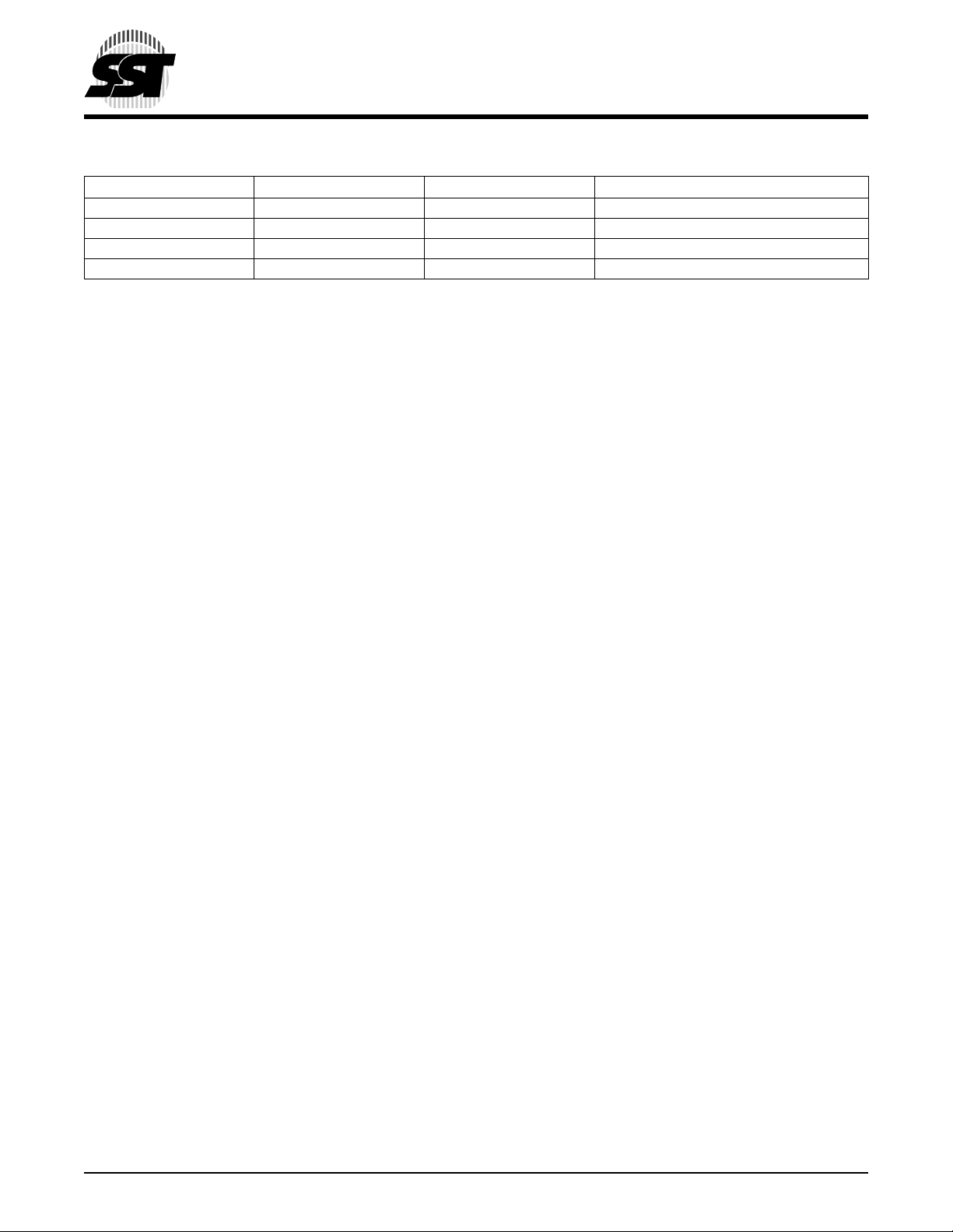
System Memory
(Top 4 MByte)
FFFFFFFFH
SST49LF002A
(2 Mbit)
SST49LF003A
(3 Mbit)
FFFC0000H
FFFA0000H
FFF80000H
SST49LF004A
(4 Mbit)
SST49LF008A
(8 Mbit)
FFF00000H
FFC00000H
BOOT-CONFIGURATION SYSTEM MEMORY MAP
Range for
Additional FWH Devices
504 ILL B1A.3
©2001 Silicon Storage Technology, Inc. S71161-06-000 9/01 504
11
 Loading...