

Silicon Storage Technology Inc SST48CF016-C1, SST48CF256-C1, SST48CF192-C1, SST48CF096-C1, SST48CF064-C1 Datasheet
...
SST48CF008 / 016 / 024 / 032 / 048 / 064 / 096 / 128 / 192 / 256
FEATURES:
CompactFlash Card
8MB / 16MB / 24MB / 32MB / 48MB / 64MB / 96MB / 128MB / 192MB / 256MB
SST48CFxxxATA/IDE Standard CompactFlash Card
Data Sheet
• CompactFlash Association specification
standard
• 8, 16, 24, 32, 48, 64, 96, 128, 192, and 256 MByte
capacities
• Small Form Factor: 36.4 mm x 42.8 mm x 3.3 mm
• Supports 5.0-Volt and 3.3-Volt Read and Write
– 4.5-5.5V, 3.135-3.465V for commercial
• PC Card ATA and True IDE interface
– 512 Bytes sector
– ATA command set compatible
• Low Power Consumption:
– Active mode: 35 mA/55 mA (3.3V/5.0V)(typical)
– Sleep mode: 100 µA/150 µA (3.3V/5.0V)(typical)
• Data Transfer Rate to/from Host
– 20 MB/s burst at 5.0V
– 6.6 MB/s burst at 3.3V
• High Performance
– Up to 1.4 MB/sec sustained write transfer rate
(host to flash)
• Controller Overhead Command to DRQ
– Less than 0.5 ms
• Zero Data Retention Power
– Batteries not required for data storage
•Start Up Time
– Sleep to Read: 200 ns
– Sleep to Write: 200 ns
– Reset to Ready: 50 ms typical, 400 ms Max.
• Support for Commercial Temperature Range
– 0°C to +70°C for operating commercial
– -25°C to +85°C non-operating (storage)
• Extremely Rugged and Reliable
– Built-in ECC support corrects 3 random Bytes
error per 512 Byte sector
– 2000 G operating and non-operating shock
• Intelligent ATA/IDE Controller
– Built-in microcontroller with intelligent firmware
– 256 Bytes of attribute memory for storing CIS
information
– Supports multiple-sector Read/Write operation
to enhance system performance
• Power Management Unit
– Immediate disabling of unused circuitry
PRODUCT DESCRIPTION
SST’s CompactFlash (CF) card is an ultra-small, low cost,
high performance, re movable flash memory data s torage
system. This te chnolo gy is well suited for soli d state mas s
storage por table applications offering new and expanded
functionality while enabling smaller and lighter designs.
CompactFlash technology is widely used in a variety of
consumer products such as portable computers, digital
cameras, handheld data collection scanners, Personal
Digital Assistants (PDAs), handy terminals, audio players,
monitoring devices and set-top bo xes .
SST’s CompactFlash products provide complete PCMCIAATA functionality and compatibility. This is achieved
because the 50- pin CF card can be e asily slipped into a
passive 68-pin Type II adapter ca rd that ful ly meets PCMCIA electrical and mechanical interface specifications.
SST’s CompactFlash products are also fully compliant with
©2001 Silicon Storage Technology, Inc.
S71125-03-000 9/01 375
1
SST is an authorized licensee of the CompactFlash™ and CF[logo]™ trademarks. Some data and tables are reproduced from the
CompactFlash Specification by permission of the CompactFlash Association. These specifications are subject to change without notice.
CFA standards. The SST CF card is read and written to
using a single power supply of 5.0V or 3.3V and is available
in 8 to 256 MByte densities.
SST’s CompactFlash cards contain additional attribute
memory of 256 Bytes for storing the Card Information
Structure (CIS) information. SST’s CompactFlash card has
built in microcontrolle r and file ma nagement fir mware that
communicates with ATA standard interfaces; there fore, the
SST’s CompactFlash cards do not requ ire additional software for the host, such as Flash File System (FFS) and
Memory Technology Driver (MTD).
The SST logo and SuperFlash are registered trademarks of Silicon Storage Technology, Inc.

CompactFlash Card
SST48CF008 / 016 / 024 / 032 / 048 / 064 / 096 / 128 / 192 / 256
Data Sheet
TABLE OF CONTENTS
PRODUCT DESCRIPTION . . . . . . . . . . . . . . . . . . . . . . . . . . . . . . . . . . . . . . . . . . . . . . . . . . . . . . . . . . . . . . . . . . . 1
1.0 GENERAL DESCRIPTION . . . . . . . . . . . . . . . . . . . . . . . . . . . . . . . . . . . . . . . . . . . . . . . . . . . . . . . . . . . . . . . 5
1.1 Performance-optimized ATA Controller . . . . . . . . . . . . . . . . . . . . . . . . . . . . . . . . . . . . . . . . . . . . . . . . . . 5
1.1.1 Microcontroller Unit (MCU). . . . . . . . . . . . . . . . . . . . . . . . . . . . . . . . . . . . . . . . . . . . . . . . . . . . . . . 5
1.1.2 Internal Direct Memory Access (DMA) Control . . . . . . . . . . . . . . . . . . . . . . . . . . . . . . . . . . . . . . . 5
1.1.3 Power Management Unit (PMU) . . . . . . . . . . . . . . . . . . . . . . . . . . . . . . . . . . . . . . . . . . . . . . . . . . 5
1.1.4 SRAM Buffer . . . . . . . . . . . . . . . . . . . . . . . . . . . . . . . . . . . . . . . . . . . . . . . . . . . . . . . . . . . . . . . . . 5
1.1.5 Embedded Flash File System . . . . . . . . . . . . . . . . . . . . . . . . . . . . . . . . . . . . . . . . . . . . . . . . . . . . 5
1.1.6 Error Correction Code (ECC). . . . . . . . . . . . . . . . . . . . . . . . . . . . . . . . . . . . . . . . . . . . . . . . . . . . . 5
1.2 SST’s CompactFlash Card Product Offering . . . . . . . . . . . . . . . . . . . . . . . . . . . . . . . . . . . . . . . . . . . . . . 6
2.0 ELECTRICAL INTERFACE . . . . . . . . . . . . . . . . . . . . . . . . . . . . . . . . . . . . . . . . . . . . . . . . . . . . . . . . . . . . . . 6
2.0.1 Pin Assignment and Pin Type . . . . . . . . . . . . . . . . . . . . . . . . . . . . . . . . . . . . . . . . . . . . . . . . . . . . 6
2.1 Electrical Description . . . . . . . . . . . . . . . . . . . . . . . . . . . . . . . . . . . . . . . . . . . . . . . . . . . . . . . . . . . . . . . . 6
2.2 Card Pin Assignment . . . . . . . . . . . . . . . . . . . . . . . . . . . . . . . . . . . . . . . . . . . . . . . . . . . . . . . . . . . . . . . . 7
2.3 Electrical Specification . . . . . . . . . . . . . . . . . . . . . . . . . . . . . . . . . . . . . . . . . . . . . . . . . . . . . . . . . . . . . . 13
2.3.1 Input Leakage Current . . . . . . . . . . . . . . . . . . . . . . . . . . . . . . . . . . . . . . . . . . . . . . . . . . . . . . . . . 13
2.3.2 Input Characteristics. . . . . . . . . . . . . . . . . . . . . . . . . . . . . . . . . . . . . . . . . . . . . . . . . . . . . . . . . . . 14
2.3.3 Output Drive Type . . . . . . . . . . . . . . . . . . . . . . . . . . . . . . . . . . . . . . . . . . . . . . . . . . . . . . . . . . . . 14
2.3.4 Output Drive Characteristics . . . . . . . . . . . . . . . . . . . . . . . . . . . . . . . . . . . . . . . . . . . . . . . . . . . . 14
2.3.5 Interface/Bus Timing . . . . . . . . . . . . . . . . . . . . . . . . . . . . . . . . . . . . . . . . . . . . . . . . . . . . . . . . . . 14
2.3.6 Attribute Memory Read Timing Specification. . . . . . . . . . . . . . . . . . . . . . . . . . . . . . . . . . . . . . . . 15
2.3.7 Configuration Register (Attribute Memory) Write Timing specification. . . . . . . . . . . . . . . . . . . . . 16
2.3.8 Common Memory Read Timing Specification . . . . . . . . . . . . . . . . . . . . . . . . . . . . . . . . . . . . . . . 17
2.3.9 Common Memory Write Timing Specification . . . . . . . . . . . . . . . . . . . . . . . . . . . . . . . . . . . . . . . 18
2.3.10 I/O Input (Read) Timing Specification . . . . . . . . . . . . . . . . . . . . . . . . . . . . . . . . . . . . . . . . . . . . 19
2.3.11 I/O Output (Write) Timing Specification . . . . . . . . . . . . . . . . . . . . . . . . . . . . . . . . . . . . . . . . . . . 20
2.3.12 True IDE Mode I/O Input (Read) Timing Specification. . . . . . . . . . . . . . . . . . . . . . . . . . . . . . . . 21
2.3.13 True IDE Mode I/O Output (Write) Timing Specification . . . . . . . . . . . . . . . . . . . . . . . . . . . . . . 22
2.4 Card Configuration. . . . . . . . . . . . . . . . . . . . . . . . . . . . . . . . . . . . . . . . . . . . . . . . . . . . . . . . . . . . . . . . . 23
2.4.1 Attribute Memory Function. . . . . . . . . . . . . . . . . . . . . . . . . . . . . . . . . . . . . . . . . . . . . . . . . . . . . . 24
2.4.2 Configuration Option Register (Address 200H in Attribute Memory) . . . . . . . . . . . . . . . . . . . . . . 24
2.4.3 Card Configuration and Status Register (Address 202H in Attribute Memory) . . . . . . . . . . . . . . 25
2.4.4 Pin Replacement Register (Address 204H in Attribute Memory) . . . . . . . . . . . . . . . . . . . . . . . . . 26
2.4.5 Socket and Copy Register (Address 206H in Attribute Memory) . . . . . . . . . . . . . . . . . . . . . . . . . 26
2.5 I/O Transfer Function. . . . . . . . . . . . . . . . . . . . . . . . . . . . . . . . . . . . . . . . . . . . . . . . . . . . . . . . . . . . . . . 27
2.5.1 I/O Function . . . . . . . . . . . . . . . . . . . . . . . . . . . . . . . . . . . . . . . . . . . . . . . . . . . . . . . . . . . . . . . . . 27
2.6 Common Memory Transfer Function . . . . . . . . . . . . . . . . . . . . . . . . . . . . . . . . . . . . . . . . . . . . . . . . . . . 28
2.6.1 Common Memory Function . . . . . . . . . . . . . . . . . . . . . . . . . . . . . . . . . . . . . . . . . . . . . . . . . . . . . 28
2.7 True IDE Mode I/O Transfer Function . . . . . . . . . . . . . . . . . . . . . . . . . . . . . . . . . . . . . . . . . . . . . . . . . . 29
2.7.1 True IDE Mode I/O Function . . . . . . . . . . . . . . . . . . . . . . . . . . . . . . . . . . . . . . . . . . . . . . . . . . . . 29
©2001 Silicon Storage Technology, Inc. S71125-03-000 9/01 375
2

CompactFlash Card
SST48CF008 / 016 / 024 / 032 / 048 / 064 / 096 / 128 / 192 / 256
Data Sheet
3.0 SOFTWARE INTERFACE . . . . . . . . . . . . . . . . . . . . . . . . . . . . . . . . . . . . . . . . . . . . . . . . . . . . . . . . . . . . . . 30
3.1 CF-ATA Drive Register Set Definition and Protocol. . . . . . . . . . . . . . . . . . . . . . . . . . . . . . . . . . . . . . . . 30
3.1.1 I/O Primary and Secondary Address Configurations . . . . . . . . . . . . . . . . . . . . . . . . . . . . . . . . . . 30
3.1.2 Contiguous I/O Mapped Addressing . . . . . . . . . . . . . . . . . . . . . . . . . . . . . . . . . . . . . . . . . . . . . . 31
3.1.3 Memory Mapped Addressing . . . . . . . . . . . . . . . . . . . . . . . . . . . . . . . . . . . . . . . . . . . . . . . . . . . . 32
3.1.4 True IDE Mode Addressing . . . . . . . . . . . . . . . . . . . . . . . . . . . . . . . . . . . . . . . . . . . . . . . . . . . . . 33
3.1.5 CF-ATA Registers . . . . . . . . . . . . . . . . . . . . . . . . . . . . . . . . . . . . . . . . . . . . . . . . . . . . . . . . . . . . 33
3.1.5.1 Data Register . . . . . . . . . . . . . . . . . . . . . . . . . . . . . . . . . . . . . . . . . . . . . . . . . . . . . . . . . 33
3.1.5.2 Error Register . . . . . . . . . . . . . . . . . . . . . . . . . . . . . . . . . . . . . . . . . . . . . . . . . . . . . . . . . 34
3.1.5.3 Feature Register . . . . . . . . . . . . . . . . . . . . . . . . . . . . . . . . . . . . . . . . . . . . . . . . . . . . . . . 34
3.1.5.4 Sector Count Register. . . . . . . . . . . . . . . . . . . . . . . . . . . . . . . . . . . . . . . . . . . . . . . . . . . 34
3.1.5.5 Sector Number (LBA 7-0) Register . . . . . . . . . . . . . . . . . . . . . . . . . . . . . . . . . . . . . . . . . 34
3.1.5.6 Cylinder Low (LBA 15-8) Register. . . . . . . . . . . . . . . . . . . . . . . . . . . . . . . . . . . . . . . . . . 34
3.1.5.7 Cylinder High (LBA 23-16) Register . . . . . . . . . . . . . . . . . . . . . . . . . . . . . . . . . . . . . . . . 34
3.1.5.8 Drive/Head (LBA 27-24) Register . . . . . . . . . . . . . . . . . . . . . . . . . . . . . . . . . . . . . . . . . . 35
3.1.5.9 Status & Alternate Status Registers . . . . . . . . . . . . . . . . . . . . . . . . . . . . . . . . . . . . . . . . 36
3.1.5.10 Device Control Register . . . . . . . . . . . . . . . . . . . . . . . . . . . . . . . . . . . . . . . . . . . . . . . . 36
3.1.5.11 Card (Drive) Address Register . . . . . . . . . . . . . . . . . . . . . . . . . . . . . . . . . . . . . . . . . . . 37
3.2 CF-ATA Command Description . . . . . . . . . . . . . . . . . . . . . . . . . . . . . . . . . . . . . . . . . . . . . . . . . . . . . . . 37
3.2.1 CF-ATA Command Set . . . . . . . . . . . . . . . . . . . . . . . . . . . . . . . . . . . . . . . . . . . . . . . . . . . . . . . . 37
3.2.1.1 Check Power Mode - 98H or E5H. . . . . . . . . . . . . . . . . . . . . . . . . . . . . . . . . . . . . . . . . . 39
3.2.1.2 Execute Drive Diagnostic - 90H . . . . . . . . . . . . . . . . . . . . . . . . . . . . . . . . . . . . . . . . . . . 39
3.2.1.3 Erase Sector(s) - C0H. . . . . . . . . . . . . . . . . . . . . . . . . . . . . . . . . . . . . . . . . . . . . . . . . . . 40
3.2.1.4 Format Track - 50H. . . . . . . . . . . . . . . . . . . . . . . . . . . . . . . . . . . . . . . . . . . . . . . . . . . . . 40
3.2.1.5 Identify Drive - ECH. . . . . . . . . . . . . . . . . . . . . . . . . . . . . . . . . . . . . . . . . . . . . . . . . . . . . 40
3.2.1.5.1 General Configuration. . . . . . . . . . . . . . . . . . . . . . . . . . . . . . . . . . . . . . . . . . . . 42
3.2.1.5.2 Default Number of Cylinders. . . . . . . . . . . . . . . . . . . . . . . . . . . . . . . . . . . . . . . 42
3.2.1.5.3 Default Number of Heads. . . . . . . . . . . . . . . . . . . . . . . . . . . . . . . . . . . . . . . . . 42
3.2.1.5.4 Number of Unformatted Bytes per Track . . . . . . . . . . . . . . . . . . . . . . . . . . . . . 42
3.2.1.5.5 Number of Unformatted Bytes per Sector. . . . . . . . . . . . . . . . . . . . . . . . . . . . . 42
3.2.1.5.6 Default Number of Sectors per Track . . . . . . . . . . . . . . . . . . . . . . . . . . . . . . . . 42
3.2.1.5.7 Number of Sectors per Card. . . . . . . . . . . . . . . . . . . . . . . . . . . . . . . . . . . . . . . 42
3.2.1.5.8 Memory Card Serial Number . . . . . . . . . . . . . . . . . . . . . . . . . . . . . . . . . . . . . . 42
3.2.1.5.9 Buffer Type. . . . . . . . . . . . . . . . . . . . . . . . . . . . . . . . . . . . . . . . . . . . . . . . . . . . 42
3.2.1.5.10 Buffer Size . . . . . . . . . . . . . . . . . . . . . . . . . . . . . . . . . . . . . . . . . . . . . . . . . . . 42
3.2.1.5.11 ECC Count . . . . . . . . . . . . . . . . . . . . . . . . . . . . . . . . . . . . . . . . . . . . . . . . . . . 42
3.2.1.5.12 Firmware Revision . . . . . . . . . . . . . . . . . . . . . . . . . . . . . . . . . . . . . . . . . . . . . 42
3.2.1.5.13 Model Number . . . . . . . . . . . . . . . . . . . . . . . . . . . . . . . . . . . . . . . . . . . . . . . . 42
3.2.1.5.14 Read/Write Multiple Sector Count . . . . . . . . . . . . . . . . . . . . . . . . . . . . . . . . . 42
3.2.1.5.15 Capabilities. . . . . . . . . . . . . . . . . . . . . . . . . . . . . . . . . . . . . . . . . . . . . . . . . . . 43
3.2.1.5.16 PIO Data Transfer Cycle Timing Mode. . . . . . . . . . . . . . . . . . . . . . . . . . . . . . 43
3.2.1.5.17 Translation Parameters Valid . . . . . . . . . . . . . . . . . . . . . . . . . . . . . . . . . . . . . 43
3.2.1.5.18 Current Number of Cylinders, Heads, Sectors/Track . . . . . . . . . . . . . . . . . . . 43
3.2.1.5.19 Current Capacity. . . . . . . . . . . . . . . . . . . . . . . . . . . . . . . . . . . . . . . . . . . . . . . 43
3.2.1.5.20 Multiple Sector Setting . . . . . . . . . . . . . . . . . . . . . . . . . . . . . . . . . . . . . . . . . . 43
3.2.1.5.21 Advanced PIO Data Transfer Mode . . . . . . . . . . . . . . . . . . . . . . . . . . . . . . . . 43
3.2.1.5.22 Minimum PIO Transfer Cycle Time Without Flow Control . . . . . . . . . . . . . . . 43
3.2.1.5.23 Minimum PIO Transfer Cycle Time With IORDY . . . . . . . . . . . . . . . . . . . . . . 43
3.2.1.5.24 Total Sectors Addressable in LBA Mode . . . . . . . . . . . . . . . . . . . . . . . . . . . . 43
3.2.1.6 Idle - 97H or E3H. . . . . . . . . . . . . . . . . . . . . . . . . . . . . . . . . . . . . . . . . . . . . . . . . . . . . . . 44
3.2.1.7 Idle Immediate - 95H or E1H. . . . . . . . . . . . . . . . . . . . . . . . . . . . . . . . . . . . . . . . . . . . . . 44
©2001 Silicon Storage Technology, Inc. S71125-03-000 9/01 375
3

CompactFlash Card
SST48CF008 / 016 / 024 / 032 / 048 / 064 / 096 / 128 / 192 / 256
Data Sheet
3.2.1.8 Initialize Drive Parameters - 91H. . . . . . . . . . . . . . . . . . . . . . . . . . . . . . . . . . . . . . . . . . . 44
3.2.1.9 Read Buffer - E4H. . . . . . . . . . . . . . . . . . . . . . . . . . . . . . . . . . . . . . . . . . . . . . . . . . . . . . 45
3.2.1.10 Read Multiple - C4H . . . . . . . . . . . . . . . . . . . . . . . . . . . . . . . . . . . . . . . . . . . . . . . . . . . 45
3.2.1.11 Read Long Sector - 22H or 23H . . . . . . . . . . . . . . . . . . . . . . . . . . . . . . . . . . . . . . . . . . 46
3.2.1.12 Read Sector(s) - 20H or 21H. . . . . . . . . . . . . . . . . . . . . . . . . . . . . . . . . . . . . . . . . . . . . 46
3.2.1.13 Read Verify Sector(s) - 40H or 41H . . . . . . . . . . . . . . . . . . . . . . . . . . . . . . . . . . . . . . . 47
3.2.1.14 Recalibrate - 1XH . . . . . . . . . . . . . . . . . . . . . . . . . . . . . . . . . . . . . . . . . . . . . . . . . . . . . 47
3.2.1.15 Request Sense - 03H . . . . . . . . . . . . . . . . . . . . . . . . . . . . . . . . . . . . . . . . . . . . . . . . . . 47
3.2.1.16 Seek - 7XH . . . . . . . . . . . . . . . . . . . . . . . . . . . . . . . . . . . . . . . . . . . . . . . . . . . . . . . . . . 48
3.2.1.17 Set Features - EFH . . . . . . . . . . . . . . . . . . . . . . . . . . . . . . . . . . . . . . . . . . . . . . . . . . . . 48
3.2.1.18 Set Multiple Mode - C6H . . . . . . . . . . . . . . . . . . . . . . . . . . . . . . . . . . . . . . . . . . . . . . . . 49
3.2.1.19 Set Sleep Mode- 99H or E6H . . . . . . . . . . . . . . . . . . . . . . . . . . . . . . . . . . . . . . . . . . . . 50
3.2.1.20 Standby - 96H or E2H. . . . . . . . . . . . . . . . . . . . . . . . . . . . . . . . . . . . . . . . . . . . . . . . . . 50
3.2.1.21 Standby Immediate - 94H or E0H . . . . . . . . . . . . . . . . . . . . . . . . . . . . . . . . . . . . . . . . . 50
3.2.1.22 Translate Sector - 87H . . . . . . . . . . . . . . . . . . . . . . . . . . . . . . . . . . . . . . . . . . . . . . . . . 51
3.2.1.23 Wear Level - F5H . . . . . . . . . . . . . . . . . . . . . . . . . . . . . . . . . . . . . . . . . . . . . . . . . . . . . 51
3.2.1.24 Write Buffer - E8H. . . . . . . . . . . . . . . . . . . . . . . . . . . . . . . . . . . . . . . . . . . . . . . . . . . . . 52
3.2.1.25 Write Long Sector - 32H or 33H . . . . . . . . . . . . . . . . . . . . . . . . . . . . . . . . . . . . . . . . . . 52
3.2.1.26 Write Multiple Command - C5H. . . . . . . . . . . . . . . . . . . . . . . . . . . . . . . . . . . . . . . . . . . 53
3.2.1.27 Write Multiple without Erase - CDH. . . . . . . . . . . . . . . . . . . . . . . . . . . . . . . . . . . . . . . . 54
3.2.1.28 Write Sector(s) - 30H or 31H. . . . . . . . . . . . . . . . . . . . . . . . . . . . . . . . . . . . . . . . . . . . . 54
3.2.1.29 Write Sector(s) without Erase - 38H . . . . . . . . . . . . . . . . . . . . . . . . . . . . . . . . . . . . . . . 55
3.2.1.30 Write Verify - 3CH . . . . . . . . . . . . . . . . . . . . . . . . . . . . . . . . . . . . . . . . . . . . . . . . . . . . . 55
3.2.2 Error Posting . . . . . . . . . . . . . . . . . . . . . . . . . . . . . . . . . . . . . . . . . . . . . . . . . . . . . . . . . . . . . . . . 56
4.0 APPENDIX . . . . . . . . . . . . . . . . . . . . . . . . . . . . . . . . . . . . . . . . . . . . . . . . . . . . . . . . . . . . . . . . . . . . . . . . . . 57
4.1 Differences between CF-ATA and PC Card-ATA/True IDE. . . . . . . . . . . . . . . . . . . . . . . . . . . . . . . . . . 57
4.1.1 Electrical Differences . . . . . . . . . . . . . . . . . . . . . . . . . . . . . . . . . . . . . . . . . . . . . . . . . . . . . . . . . . 57
4.1.1.1 TTL Compatibility . . . . . . . . . . . . . . . . . . . . . . . . . . . . . . . . . . . . . . . . . . . . . . . . . . . . . . 57
4.1.1.2 Pull Up Resistor Input Leakage Current . . . . . . . . . . . . . . . . . . . . . . . . . . . . . . . . . . . . . 57
4.1.2 Functional Differences . . . . . . . . . . . . . . . . . . . . . . . . . . . . . . . . . . . . . . . . . . . . . . . . . . . . . . . . . 57
4.1.2.1 Additional Set Features Codes in CF-ATA . . . . . . . . . . . . . . . . . . . . . . . . . . . . . . . . . . . 57
4.1.2.2 Additional Commands in CF-ATA . . . . . . . . . . . . . . . . . . . . . . . . . . . . . . . . . . . . . . . . . . 57
4.1.2.3 Idle Timer . . . . . . . . . . . . . . . . . . . . . . . . . . . . . . . . . . . . . . . . . . . . . . . . . . . . . . . . . . . . 57
4.1.2.4 Recovery from Sleep Mode. . . . . . . . . . . . . . . . . . . . . . . . . . . . . . . . . . . . . . . . . . . . . . . 57
5.0 PHYSICAL DIMENSIONS . . . . . . . . . . . . . . . . . . . . . . . . . . . . . . . . . . . . . . . . . . . . . . . . . . . . . . . . . . . . . . 58
6.0 PRODUCT ORDERING INFORMATION . . . . . . . . . . . . . . . . . . . . . . . . . . . . . . . . . . . . . . . . . . . . . . . . . . . 59
6.1 Valid combinations. . . . . . . . . . . . . . . . . . . . . . . . . . . . . . . . . . . . . . . . . . . . . . . . . . . . . . . . . . . . . . . . . 59
7.0 LIMITED WARRANTY . . . . . . . . . . . . . . . . . . . . . . . . . . . . . . . . . . . . . . . . . . . . . . . . . . . . . . . . . . . . . . . . . 60
7.1 Life Support Policy. . . . . . . . . . . . . . . . . . . . . . . . . . . . . . . . . . . . . . . . . . . . . . . . . . . . . . . . . . . . . . . . . 60
8.0 PATENT PROTECTION. . . . . . . . . . . . . . . . . . . . . . . . . . . . . . . . . . . . . . . . . . . . . . . . . . . . . . . . . . . . . . . . 60
9.0 PCMCIA STANDARD. . . . . . . . . . . . . . . . . . . . . . . . . . . . . . . . . . . . . . . . . . . . . . . . . . . . . . . . . . . . . . . . . . 60
10.0 COMPACTFLASH SPECIFICATION . . . . . . . . . . . . . . . . . . . . . . . . . . . . . . . . . . . . . . . . . . . . . . . . . . . . . . 60
11.0 RELATED DOCUMENTS . . . . . . . . . . . . . . . . . . . . . . . . . . . . . . . . . . . . . . . . . . . . . . . . . . . . . . . . . . . . . . . 60
©2001 Silicon Storage Technology, Inc. S71125-03-000 9/01 375
4
CompactFlash Card
SST48CF008 / 016 / 024 / 032 / 048 / 064 / 096 / 128 / 192 / 256
Data Sheet
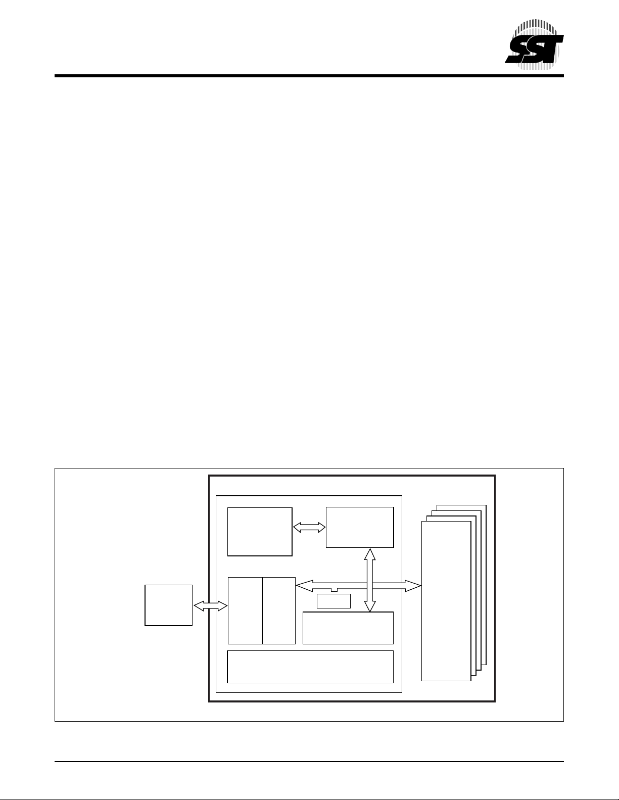
1.0 GENERAL DESCRIPTION
The SST’s CompactFlash card contains a controller,
embedded fir mware storage and flash media in a matchbook sized package with a 50-pin con nector consisti ng of
two rows of 25 female contacts each on 50 mil ( 1.27 m m)
centers. Refer to Figure 1 for SST’s CompactFlash card
block diagram. The controll er interfaces with th e host system allowing data to be wr itten to and rea d from the fla sh
media.
1.1 Performance-optimized ATA Controller
The heart of a CompactFlash card is the ATA controller
which translates standard IDE/ATA signals into flash media
data and controls. SST’s CompactFlash card contains a
proprietary ATA contro ller th at was spec ific ally de sign ed to
attain high data throughput from host to flash. The following
components contribute to the A TA controller’s performance.
1.1.1 Microcontroller Unit (MCU)
The MCU translates IDE/ATA commands into data and
control signals required for flash memory operation.
1.1.2 Internal Direct Memory Access (DMA) Control
The ATA controller inside SST’s CompactFlash card uses
DMA allowing instant data transfer to memory. This implementation eliminates controller overhead associated wit h
traditional, firmware based, memory control, increasing
data transfer rate.
1.1.3 Power Management Unit (PMU)
Power Management Unit control s the power c onsumptio n
of the CompactFlas h ca rd. T h e P MU dram ati cal ly extends
product battery life by putting the part of the circuitry that is
not in operation into sleep mode.
1.1.4 SRAM Buffer
A key contributor to the ATA controller performance is a
SRAM buffer. The buffer optimizes host’s data writes to
flash media.
1.1.5 Embedded Flash File System
Embedded Flash File System is an integral part of the
SST’s ATM contro ller. It contains MCU firmware that performs the f ollow ing tasks:
1. Translates host side signals into flash media
Writes and Reads.
2. Provides flash media wear leveling to spread the
flash writes across all the memory address space
to increase the longevity of flash media.
3. Keeps track of data file structures.
1.1.6 Error Correction Code (ECC)
The ATA Cont r ol l e r c o nt ai n s EC C al g o rithm that c o rr ec t s
3 bytes of error per 512 Byte sector.
ATA Controller
Embedded
Flash
File System
SRAM Buffer
To
Host
PMU
FIGURE 1: SST C
©2001 Silicon Storage Technology, Inc. S71125-03-000 9/01 375
OMPACTFLASH BLOCK DIAGRAM
5
MCU
Flash
Media
ECC
Internal
DMA
375 ILL1-1.4
CompactFlash Card
SST48CF008 / 016 / 024 / 032 / 048 / 064 / 096 / 128 / 192 / 256
Data Sheet
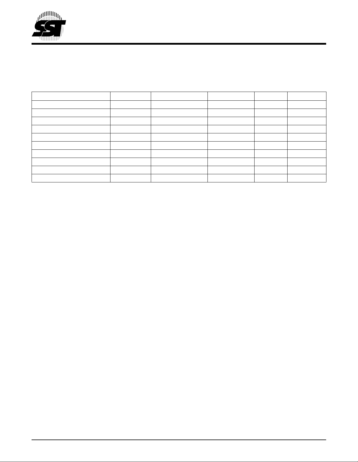
1.2 SST’s CompactFlash Card Product Offering
The SST48CFxxx High Co mpactFlash p roduct family is available in 8 to 256 MBy te densitie s. The following table
shows the specific capacity, default number of cylinder heads, sectors and cylinders for each product line.
.
Model Number Density T ota l Bytes Cylinders Heads Sectors
SST48CF008 8 MB 8,028,160 245 2 32
SST48CF016 16 MB 16,023,552 489 2 32
SST48CF024 24 MB 24,051,712 367 4 32
SST48CF032 32 MB 32,047,104 489 4 32
SST48CF048 48 MB 48,037,888 733 4 32
SST48CF064 64 MB 64,028,672 977 4 32
SST48CF096 96 MB 96,075,776 733 8 32
SST48CF128 128 MB 128,057 ,344 977 8 32
SST48CF192 192 MB 192,151 ,552 733 16 32
SST48CF256 256 MB 256,114 ,688 977 16 32
2.0 ELECTRICAL INTERFACE
2.0.1 Pin Assignment and Pin Type
The signal/pin assignments ar e listed in Table 2-1. Low active signals have a “-” p r ef ix. Pin types are Input, Output or Input/
Output. Section 2.3 defines the DC characteristics for all input and output type structures.
2.1 Electrical De scription
The CompactFlas h car d func tion s in thre e basic mode s: 1) PC Ca rd ATA using I/O Mode, 2) PC Ca rd ATA using Memor y
Mode and 3) True IDE Mode, which is compatible with most disk drives. The configuration of the CompactFlash card will be
controlled using the standard PCMCIA configuration registers starting at address 200H in the Attribute Memory space of the
storage card or for True IDE Mode, pin 9 being grounded.
Table 2-2 desc r i bes the I/O si gna ls. Si gn al s whos e s ourc e i s the hos t ar e desig nat ed as in pu ts whil e sig na ls tha t the Co mpactFlash card sources are outputs. The CompactFlash card logic levels conform to those specified in the PCMCIA Release
2.1 and CFA Specification Rev. 1.4. As shown in Table 2-2, each signal ha s three pos sible operating modes : 1) PC Card
Memory, 2) PC Card I/O and 3) True IDE. All outputs fro m the card ar e tot em po le e x cept th e dat a bu s sign als wh ic h are bi directional tri-state. Refer to Section 2.3 for definitions of Input and Output type.
©2001 Silicon Storage Technology, Inc. S71125-03-000 9/01 375
6
CompactFlash Card
SST48CF008 / 016 / 024 / 032 / 048 / 064 / 096 / 128 / 192 / 256
Data Sheet
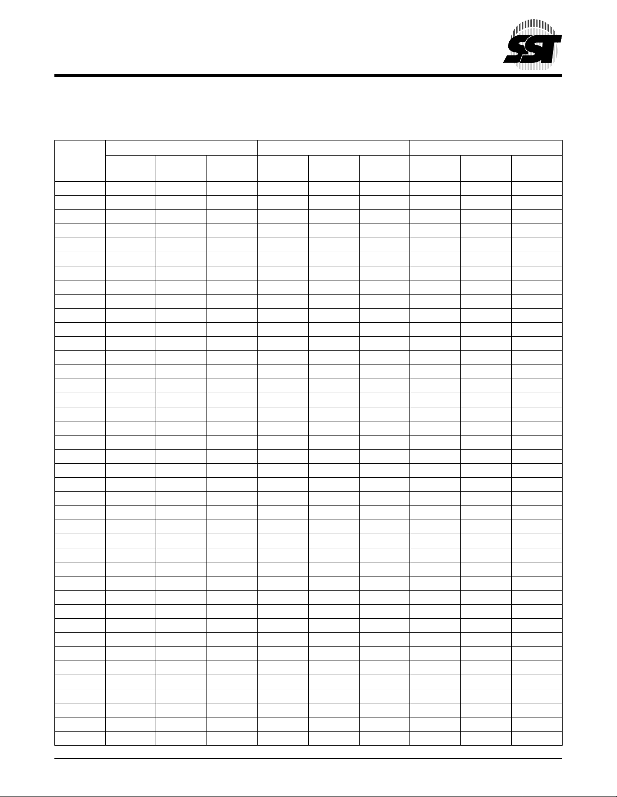
2.2 Card Pin Assignment
TABLE 2-1: CARD PIN ASSIGNMENT (1 OF 2)
Memory card mode I/O card mode True IDE mode
Signal
1
Name Pin Type I/O Type
Pin No.
Signal
Name Pin Type I/O Type
1 GND - GND GND - GND GND - GND
2D
3D
4D
5D
3
4
5
6
I/O I2D , O2 D
I/O I2D , O2 D
I/O I2D , O2 D
I/O I2D , O2 D
6D7I/O I2D , O2 D
3
4
5
6
7
I/O I2D , O2 D
I/O I2D , O2 D
I/O I2D , O2 D
I/O I2D , O2 D
I/O I2D , O2 D
7-CE1I I3U-CE1I I3U-CS0I I3U
8 A10 I I2D A10 I I2D A10 I I2D
9 -OE I I3U -OE I I3U -ATASEL I I3U
10 A
11 A
12 A
13 V
14 A
15 A
16 A
17 A
18 A
19 A
20 A
21 D
22 D
23 D
9
8
7
DD
6
5
4
3
2
1
0
0
1
2
II2DA9II2DA9II2D
II2DA8II2DA8II2D
II2DA7II2DA7II2D
-- VDD-- VDD-II2DA6II2DA6II2D
II2DA5II2DA5II2D
II2DA4II2DA4II2D
II2DA3II2DA3II2D
II2DA2II2DA2II2D
II2DA1II2DA1II2D
II2DA0II2DA0II2D
I/O I2D , O2 D
I/O I2D , O2 D
I/O I2D , O2 D
0
1
2
I/O I2D , O2 D
I/O I2D , O2 D
I/O I2D , O2 D
24 WP O O2 -IOIS16 O O2 -IOIS16 O O2
25 -CD2 O Ground -CD2 O Ground -CD2 O Ground
26 -CD1 O Ground -CD1 O Ground -CD1 O Ground
27 D
28 D
29 D
30 D
31 D
11
12
13
14
15
I/O I2D , O2 D
I/O I2D , O2 D
I/O I2D , O2 D
I/O I2D , O2 D
I/O I2D , O2 D
11
12
13
14
15
I/O I2D , O2 D
I/O I2D , O2 D
I/O I2D , O2 D
I/O I2D , O2 D
I/O I2D , O2 D
32 -CE2 I I3U -CE2 I I3U -CS1 I I3U
33 -VS1 O Ground -VS1 O Ground -VS1 O Ground
34 -IORD I I3U -IORD I I3U -IORD I I3U
35 -IOWR I I3U -IOWR I I3U -IOWR I I3U
36 -WE I I3U -WE I I3U -WE I I3U
37 RDY/-BSY O O1 -IREQ O O1 INTRQ O O1
38 V
DD
-- VDD-- VDD-39 -CSEL I I2U -CSEL I I2U -CSEL I I2U
40 -VS2 O open -VS2 O open -VS2 O open
Signal
1
Name Pin Type I/O Type
3
4
5
6
7
0
1
2
11
12
13
14
15
I/O I2D, O2
I/O I2D, O2
I/O I2D, O2
I/O I2D, O2
I/O I2D, O2
I/O I2D, O2
I/O I2D, O2
I/O I2D, O2
I/O I2D, O2
I/O I2D, O2
I/O I2D, O2
I/O I2D, O2
I/O I2D, O2
1
©2001 Silicon Storage Technology, Inc. S71125-03-000 9/01 375
7
CompactFlash Card
SST48CF008 / 016 / 024 / 032 / 048 / 064 / 096 / 128 / 192 / 256
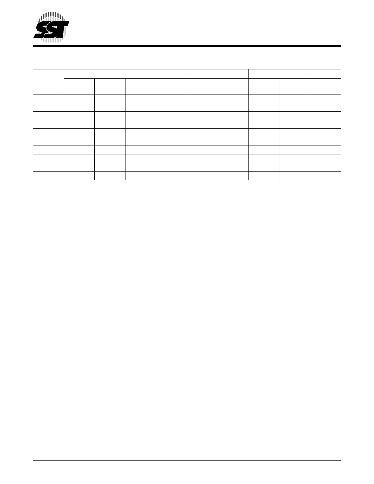
TABLE 2-1: CARD PIN ASSIGNMENT (CONTINUED) (2 OF 2)
Memory card mode I/O card mode True IDE mode
Signal
1
Name Pin Type I/O Type
Pin No.
Signal
Name Pin Type I/O Type
41 RESET I I4U RESET I I4U -RESET I I4U
42 -WAIT O O1 -WAIT O O1 IORDY O O1
43 -INPACK O O1 -INPACK O O1 -INPACK O O1
44 -REG I I3U -REG I I3U -REG I I3U
45 BVD2 O I2U, O1 -SPKR O I2U, O1 -DASP O I2U, O1
46 BVD1 O I2U, O1 -STSCHG O I2U, O1 -PDIAG O I2U, O1
47 D
48 D
49 D
8
9
10
I/O I2D , O2 D
I/O I2D , O2 D
I/O I2D , O2 D
8
9
10
I/O I2D , O2 D
I/O I2D , O2 D
I/O I2D , O2 D
50 GND - GND GND - GND GND - GND
1. Please refer to Sections 2.3.1 to 2.3.4 for detail.
Signal
1
Name Pin Type I/O Type
8
9
10
I/O I2D, O2
I/O I2D, O2
I/O I2D, O2
Data Sheet
1
T2-1.2 375
©2001 Silicon Storage Technology, Inc. S71125-03-000 9/01 375
8
CompactFlash Card
SST48CF008 / 016 / 024 / 032 / 048 / 064 / 096 / 128 / 192 / 256
Data Sheet
TABLE 2-2: SIGNAL DESCRIPTION (1 OF 4)
Symbol Type
- A
A
10
0
(PC Card Memory Mode)
- A
A
10
0
(PC Card I/O Mode)
A
- A
2
0
(True IDE Mode
BVD1
(PC Card Memory Mode)
-STSCHG
(PC Card I/O Mode)
Status Changed -PDIAG
(True IDE Mode)
BVD2
(PC Card Memory Mode)
-SPKR
(PC Card I/O Mode)
-DASP
(True IDE Mode)
-CD1, -CD2
(PC Card Memory Mode)
-CD1, -CD2
(PC Card I/O Mode)
-CD1, -CD2
(True IDE Mode)
-CE1, -CE2
(PC Card Memory Mode)
Card Enable
-CE1, -CE2
(PC Card I/O Mode)
Card Enable
-CS0, -CS1
(True IDE Mode)
1
I 8,10,11,12,
Pin Name and Functions
These address lines along with the -REG signa l are used to selec t
14,15,16,17,
18,19,20
the following: The I/O port address registers within the CompactFlash card, the memory mapped port address registers within the
CompactFlash card, a byte in the card’s information s tructure and its
configuration control and status registers.
This signal is the same as the PC Card Memory Mode signal
I 18,19,20 In True IDE Mode only A[2:0] are used to select the one of e ight (True
IDE Mode) registers in the Task File, the remaining address lines
should be grounded by the host.
I/O 46 This s ignal i s asse rted high as the BVD1 sig nal sin ce a bat tery is not
used with this product.
This signal is asserted low to alert the host to changes in the RDY/-
BSY and Write Protect states, while the I/O interface is configured.
Its use is controlled by the Card Config and Status Register.
In the True IDE Mode, this input/output is the Pass Diagnostic signal
in the Master/Slave handshake proto co l.
I/O 45 This output line is always driven to a high state in Memory Mode
since a battery is not required for this product.
This output line is a lways driven to a high state in I /O Mode s ince this
product does not support the audio function.
In the True IDE Mode, this input/output is the Disk Active/Slave
Present signal in the Master/Slave handshake protocol.
O 26,25 These Card Detect pins are connected to ground on the Compact-
Flash card. They are used by the host to determine that the CompactFlash card is fully inserted into its socket.
This signal is the same for all modes.
This signal is the same for all modes.
I 7,32 These input signals are used both to select the card and to indicate
to the card whether a byte or a word operation is being performed. CE2 always accesses the Odd Byte of the word. -CE1 accesses the
Even Byte or the O dd Byte of the wo rd depe nding on A
multiplexing scheme based on A
access all data on D
0-D7
.
, -CE1, -CE2 allows 8 bit hosts to
0
See Tables 2-11, 2-13, 2-16, 2-17, and 2-18.
This signal is the same as the PC Card Memory Mode signal.
In the True IDE Mode CS0 is the chip select f or th e ta sk fil e reg is ters
while CS2 is used to select the Alternate Status Register and the
Device Control Register.
and -CE2. A
0
©2001 Silicon Storage Technology, Inc. S71125-03-000 9/01 375
9
SST48CF008 / 016 / 024 / 032 / 048 / 064 / 096 / 128 / 192 / 256
TABLE 2-2: SIGNAL DESCRIPTION (CONTINUED) (2 OF 4)
Symbol Type
-CSEL
(PC Card Memory Mode)
-CSEL
(PC Card I/O Mode)
-CSEL
(True IDE Mode)
D15 - D00
(PC Card Memory Mode)
D15 - D00
(PC Card I/O Mode)
D15 - D00
(True IDE Mode)
GND
(PC Card Memory Mode)
GND
(PC Card I/O Mode)
GND
(True IDE Mode)
-INPACK
(PC Card Memory Mode)
-INPACK
(PC Card I/O Mode)
Input Acknowledge
-INPACK
(True IDE Mode)
-IORD
(PC Card Memory Mode)
-IORD
(PC Card I/O Mode)
-IORD
(True IDE Mode)
-IOWR
(PC Card Memory Mode)
-IOWR
(PC Card I/O Mode)
-IOWR
(True IDE Mode)
1
I 39 This signal is not used for this mode.
I/O 31,30,29,28,
- 1,50 Ground.
O 43 This signal is not used in this mode.
I 34 This signal is not used in this mode.
I 35 This signal is not used in this mode.
Pin Name and Functions
This signal is not used for this mode.
This internally pulled up signal is used to configure this device as a
Master or a Slave when configured in the True IDE Mode. When this
pin is grounded, this device is configured as a Master. When the pin
is open, this device is configured as a Slave.
These lines carry the Data, Commands and Status information
27,49,48,47,
6,5,4,3,2,
23, 22, 21
between the host and th e cont roller. D00 is the LSB of the Even Byte
of the Word. D08 is the LSB of the Odd Byte of the Word.
This signal is the same as the PC Card Memory Mode signal.
In True IDE Mode, all Task File operations occur i n Byte-M ode o n the
low order bus D00-D07 while all data transfers are 16 bit using D00D15.
This signal is the same for all modes.
This signal is the same for all modes.
The Input Acknowledge signal is asserted by the CompactFlash
Card when the card is selected and responding to an I/O read cycle
at the address that is on the address bus. This signal is used by the
host to control the enab le o f any input da ta b uff ers betw een th e CompactFlash card and the CPU.
In True IDE Mode this output signal is not used and should not be
connected at the host.
This is an I/O Read strobe generated by the host. This signal gates
I/O data onto the bus from the CompactFlash Card when the card is
configured to use the I/O interface.
In True IDE Mode, this signal has the same fun cti on as in PC Card
I/O Mode.
The I/O Write strobe pulse is used to clock I/O data on the Card Data
bus into the CompactFlash card controller registers when the CompactFlash card is configured to use the I/O interface.
The clocking will occur on the negative to positive edge of the signal
(trailing edge). In True IDE Mode, this signal has the same function
as in PC Card I/O Mode.
CompactFlash Card
Data Sheet
©2001 Silicon Storage Technology, Inc. S71125-03-000 9/01 375
10
CompactFlash Card
SST48CF008 / 016 / 024 / 032 / 048 / 064 / 096 / 128 / 192 / 256
Data Sheet
TABLE 2-2: SIGNAL DESCRIPTION (CONTINUED) (3 OF 4)
Symbol Type
-OE
(PC Card Memory Mode)
-OE
(PC Card I/O Mode)
-ATA SEL
(True IDE Mode)
RDY/-BSY
PC Card Memor y Mode)
-IREQ
PC Card I/O Mode)
INTRQ
(True IDE Mode)
-REG
(PC Card Memory Mode)
-REG
PC Card I/O Mode)
-REG
(True IDE Mode)
RESET
(PC Card Memory Mode)
RESET
(PC Card I/O Mode)
-RESET
(True IDE Mode)
V
DD
(PC Card Memory Mode)
V
DD
(PC Card I/O Mode)
V
DD
(True IDE Mode)
1
Pin Name and Functions
I 9 This is an Output Enable strobe generated by the host interface. It is
used to read data from the Co mpac tFlash card i n Mem ory Mode and
to read the CIS and configuration registers.
In PC Card I/O Mode, this signal is used to read the CIS and configuration registers.
To enable True IDE Mode this input should be grounded by the host.
O 37 In Mem ory Mode this s ignal is s et high w hen the Co mpactFla sh Card
is ready to accept a new data transfer operation and held low when
the card is busy. The Host memory card socket must provide a pullup resistor.
At power up and at Reset, the RDY/-BSY signal is held low (busy)
until the CompactFlash card has completed its power up or reset
function. No access of any type should be made to the CompactFlash card during this time. The RDY/-BSY signal is held high (disabled from being busy) whenever the following condition is true: The
CompactFlash Card has been powered up with +RESET continuously disconnected or asserted.
I/O Operation - A fter the Compac tFlash c ard ha s been confi gured f or
I/O operation, this signal is used as -Interrupt Request. This line is
strobed low to gen erate a pulse mod e i nte rrupt or he ld low fo r a l evel
mode interrupt.
In True IDE Mode signal is the active high Interrupt Request to the
host.
I 44 This signal is used during Memory Cycles to distinguish between
Common Memory and Register (Attribute) M emory Attribute Memory
Select accesses. High for Common Memory, Low for Attribute Memory.
The signal must also be active (low) during I/O Cycles when the I/O
address is on the Bus.
In True IDE Mode this input signal is not used and should be connected to V
by the host.
DD
I 41 When the pin is high, t his signal Resets th e Comp actFlash Card. The
CompactFlash card i s R ese t o nl y at po wer up if this p in is l eft hi gh or
open from power-up . The Compa ctFlash card is also Res et when the
Soft Reset bit in the Card Configuration Option Register is set.
This signal is the same as the PC Card Memory Mode signal.
In the True IDE Mode this input pin is the active low hardware reset
from the host.
- 13,38 +5.0V, +3.3V power.
This signal is the same for all modes.
This signal is the same for all modes.
©2001 Silicon Storage Technology, Inc. S71125-03-000 9/01 375
11
SST48CF008 / 016 / 024 / 032 / 048 / 064 / 096 / 128 / 192 / 256
TABLE 2-2: SIGNAL DESCRIPTION (CONTINUED) (4 OF 4)
Symbol Type
-VS1
-VS2
(PC Card Memory Mode)
-VS1
-VS2
(PC Card I/O Mode)
-VS1
-VS2
(True IDE Mode)
-WAIT
(PC Card Memory Mode)
-WAIT
(PC Card I/O Mode)
1
Pin Name and Functions
O3340Voltage Sense Signals. -VS1 is grounded so that the CompactFlash
card CIS can be read at 3.3V and -VS2 i s r ese rved by PCMCIA for a
secondary voltage.
This signal is the same for all modes.
This signal is the same for all modes.
O 42 The -WAIT signal is driven low by the CompactFlash
Card to signal the host to delay completion of a memory or I/O cycle
that is in progress.
This signal is the same as the PC Card Memory Mode signal.
CompactFlash Card
Data Sheet
IORDY
(True IDE Mode)
-WE
(PC Card Memory Mode)
-WE
(PC Card I/O Mode)
-WE
(True IDE Mode)
WP
(PC Card Memory Mode)
Write Protect
-IOIS16
(PC Card I/O Mode)
-IOIS16
(True IDE Mode)
1. I = Input
0 = Output
In True IDE Mode this output signal may be used as IORDY.
I 36 This is a signal driven by the host and used for strobing memory
write data to the registers of the CompactFlash card when the card is
configured in the memory interface mode. It is also used for writing
the configuration registers.
In PC Card I/O Mode, this signal is used for writing the configuration
registers.
In True IDE Mode this input signal is not used and should be connected to V
by the host.
DD
O 24 Memory Mode - The CompactFlash card does not have
a write protect switch. This signal is held low after the completion
of the reset initialization sequence.
I/O Operation - When the CompactFlash card is configured for I/O
Operation Pin 24 is u sed f or the -I/O Selec ted i s 16 Bit Port (-IOIS16)
function. A Low signal indicates that a 16 bit or Odd Byte only operation can be performed at the addressed port.
In True IDE Mode this output signal is asserted low when this device
is expecting a word data transfer cycle.
T2-2.0 375
©2001 Silicon Storage Technology, Inc. S71125-03-000 9/01 375
12
CompactFlash Card
SST48CF008 / 016 / 024 / 032 / 048 / 064 / 096 / 128 / 192 / 256
Data Sheet
2.3 Electrical Specification
The following table defines all D.C. Characteristics for the SST CompactFlash card product family.
Unless otherwise stated, conditions are:
Non operating (storage) temperature range -25°C to +85°C
V
= 4.5-5.5V
DD
V
= 3.135-3.465V
DD
Ta = 0°C to +70°C
BSOLUTE MAXIMUM CONDITIONS
A
Parameter Symbol Conditions
Input Powe r V
Voltage on any pin except VDD with respect to GND V -0.5V min. to VDD + 0.5V Max
DD
INPUT POWER
Maximum Average RMS
Voltage
3.135-3.465V 75 mA 200 µA 3.3V at 25°C
4.5-5.5V 100 mA 300 µA 5.0V at 25°C
Active Current
Maximum Average RMS
Sleep Current Measurement Method
-0.3V min. to 6.5V Max
1
1
1. Current measurement is accomplished by connecting an amp meter (set to the 2 amp scale range) in series with the VDD supply to
the CompactFlash card. Current measurements are to be taken while looping on a data transfer command with a sector count of 128.
Current consumption values for both Read and Write commands are not to exceed the Maximum Average RMS Current specified in
this table
CompactFlash produc ts shal l opera te cor rec tl y in bot h voltage ranges as sh own in the table above. To compl y wit h
this specification, current requirements must not exceed the maximum limit.
2.3.1 Input Leakage Current
In the table below, x refers to the characteristics descr ibed in Sectio n 2.3.2. For example, I1U indicates a pul l up
resistor with a type 1 input characteristic.
Type Parameter Symbol Conditions Min Typ Max Units
V
IxZ Input Leakage Current IL
IxU Pull Up Resistor RPU1 VDD = 5.0V 50k 500k Ohm
IxD Pull Down Resistor RPD1 VDD = 5.0V 50k 500k Ohm
= VDD / VIL = GND -1 1 µA
IH
©2001 Silicon Storage Technology, Inc. S71125-03-000 9/01 375
13
SST48CF008 / 016 / 024 / 032 / 048 / 064 / 096 / 128 / 192 / 256
2.3.2 Input Characteristics
Type Parameter Symbol
1 Input Voltage
CMOS
2 Input Voltage
CMOS
3 Input Voltage V
CMOS Schmitt Trigger
4 Input Voltage CMOS V
Schmitt Trigger V
2.3.3 Output Drive Type
All output drive type are CMOS level.
2.3.4 Output Drive Characteristics
CompactFlash Card
Data Sheet
Min Typ Max Min Typ Max Units
VDD = 3.3V VDD = 5.0V
V
2.4 2.4 Volts
IH
V
IL
V
2.0 2.7 Volts
IH
V
IL
TH
V
TL
TH
TL
2.0 2.4 Volts
0.5 0.8
1.8 2.4 Volts
0.9 0.8
0.6 0.8
0.8 0.8
Type Parameter Symbol Conditions Min Typ Max Units
O1 Output Voltage VOH I
V
OL
O2 Output Voltage V
I
OH
V
OL
= -4 mA V
OH
-0.8V Volts
DD
IOL = 4 mA GND +0.4V
= -8 mA V
OH
-0.8V Volts
DD
IOL = 8 mA GND +0.4V
2.3.5 Interface/Bus Timing
There are two types of bus cycles and timing sequences that occur in the PCMCIA type interface, a direct mapped
I/O transfer and a memory access. The two timing sequences are explained in detail in the PCMCIA PC Card Standard. SST’s CompactFlash card conforms to the timing in that reference document.
©2001 Silicon Storage Technology, Inc. S71125-03-000 9/01 375
14
CompactFlash Card
SST48CF008 / 016 / 024 / 032 / 048 / 064 / 096 / 128 / 192 / 256
Data Sheet
2.3.6 Attribute Memory Read Timing Specification
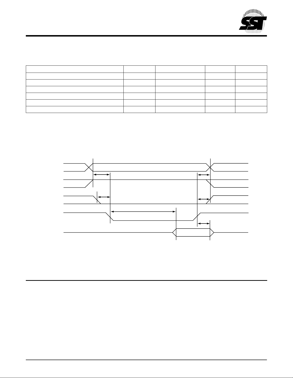
The Attribute Memory access time is defined as 100 ns. Detailed timing specifications are shown in Table 2-3.
TABLE 2-3: ATTRIBUTE MEMORY READ TIMING
Speed Version 100 ns
Item Symbol IEEE Symbol Min
Read Cycle Time tc(R) tAVAV 100
Address Access Time ta(A) tAVQV 100
Card Enable Access Time ta(CE) tELQV 100
Output Enable Access Time ta(OE) tGLQV 50
Output Disable Time from CE tdis(CE) tEHQZ 50
Output Disable Time from OE tdis(OE) tGHQZ 50
Address Setup Time tsu(A) tAVGL 10
Output Enable Time from CE ten(CE) tELQNZ 5
Output Enable Time from OE ten(OE) tGLQNZ 5
Data Valid from Address Change tv(A) tAXQX 0
1. All times are in nanoseconds. D
signal and the -WE signal must be de-asserted between consecutive cycle operations.
All AC specifications are guaranteed by design.
signifies data provided by the CompactFlash card to the system. The -CE signal or both the -OE
OUT
1
Max
T2-3.1 375
1
tc(R)
An
-REG
tsu(A)
ta(A)
ta(CE)
-CE
ten(CE)
ta(OE)
-OE
ten(OE)
Dout
FIGURE 2-1: ATTRIBUTE MEMORY READ TIM I N G DIAGRAM
tv(A)
tdis(CE)
tdis(OE)
Dout
375 ILL2-1.0
©2001 Silicon Storage Technology, Inc. S71125-03-000 9/01 375
15
CompactFlash Card
SST48CF008 / 016 / 024 / 032 / 048 / 064 / 096 / 128 / 192 / 256
Data Sheet
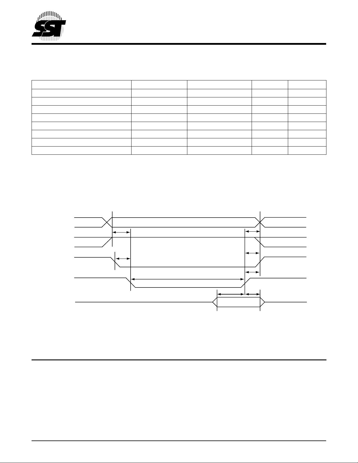
2.3.7 Configuration Register (Attribute Memory) Write Timing specification
The Card Configuration write access time is defined as 100 ns. Detailed timing specifications are shown in Table 2-4.
TABLE 2-4: CONFIGURATION REGISTER (ATTRIBUTE MEMORY) WRITE TIMING
Speed Version 100 ns
Item Symbol IEEE Symbol Min
Write Cycle Time tc(W) tAVAV 100
Write Pulse Width tw(WE) tWLWH 60
Address Setup Time tsu(A) tAVWL 10
Write Recovery Time trec(WE) tWMAX 15
Data Setup Time for WE tsu(D-WEH) tDVWH 40
Data Hold Time th(D) tWMDX 15
1. All times are in nanoseconds. DIN signifies data provided by the system to the CompactFlash card.
All AC specifications are guaranteed by design.
1
Max
T2-4.1 375
1
tc(W)
-Reg
An
tsu(A)
tw(WE)
trec(WE)
-WE
tsu(D-WEH)
-CE
-OE
Din
FIGURE 2-2: CONFIGURATION REGISTER (ATTRIBUTE MEMORY) WRITE TIMING DIAGRAM
Din Valid
375 ILL2-2.0
th(D)
©2001 Silicon Storage Technology, Inc. S71125-03-000 9/01 375
16
CompactFlash Card
SST48CF008 / 016 / 024 / 032 / 048 / 064 / 096 / 128 / 192 / 256
Data Sheet
2.3.8 Common Memory Read Timing Specification
TABLE 2-5: COMMON MEMORY READ TIMING
Item Symbol IEEE Symbol Min1 ns
Output Enable Access Time ta(OE) tGLQV 50
Output Disable Time from OE tdis(OE) tGHQZ 50
Address Setup Time tsu(A) tAVGL 10
Address Hold Time th(A) tGHAX 15
CE Setup before OE ts u(CE ) tELGL 0
CE Hold following OE th(CE) tGHEH 15
1. All times are in nanoseconds.
All AC specifications are guaranteed by design.
Max1 ns
T2-5.1 375
An
tsu(A)
-REG
-CE
tsu(CE)
ta(OE)
-OE
Dout
FIGURE 2-3: CO MMON MEM ORY READ TIMING DIAGRAM
th(A)
th(CE)
tdis(OE)
Dout
375 ILL2-3.0
©2001 Silicon Storage Technology, Inc. S71125-03-000 9/01 375
17
CompactFlash Card
SST48CF008 / 016 / 024 / 032 / 048 / 064 / 096 / 128 / 192 / 256
2.3.9 Common Memory Write Timing Specification
TABLE 2-6: COMMON MEMORY WRITE TIMING
Item Symbol IEEE Symbol Min1 ns
Data Setup before WE tsu(D-WEH) tDVWH 40
Data Hold following WE th(D) tWMDX 15
WE Pulse Width tw(WE) tWLWH 60
Address Setup Time tsu(A) tAVWL 10
CE Setup before WE tsu(CE) tELWL 0
Write Recovery Time trec(WE) tWMAX 15
Address Hold Time th(A) tGHAX 15
CE Hold following WE th(CE) tGHEH 15
1. All times are in nanoseconds.
All AC specifications are guaranteed by design.
Data Sheet
Max1 ns
T2-6.1 375
An
tsu(A)
-REG
-CE
tsu(CE)
tw(WE)
-WE
Din
tsu(D-WEH)
FIGURE 2-4: CO MMON MEM ORY WRITE TIMING DIAGRAM
th(A)
th(CE)
trec(WE)
th(D)
Din Valid
375 ILL2-4.0
©2001 Silicon Storage Technology, Inc. S71125-03-000 9/01 375
18
 Loading...