

Silicon Storage Technology Inc SST45LF010-10-4C-SA, SST45LF010-10-4C-QA Datasheet

FEATURES:
1 Megabit Serial Flash
SST45LF010
SST45LF0101Mb Serial Architecture Interface flash memory
Data Sheet
• Single 3.0-3.6V Read and Write Operations
• Serial Interface Architecture
• Byte Serial Read with Single Command
• Superior Reliability
– Endurance: 100,000 Cycles (typical)
– Greater than 100 years Data Retention
• Low Power Consumption
– Ac ti ve Current: 10 mA (typical)
– Standby Current: 10 µA (typical)
• Sector or Chip-Erase Capability
– Uniform 4 KByte sectors
• Fast Erase and Byte-Program
– Chip-Erase Time: 70 ms (typical)
– Sector-Erase Time: 18 ms (typical)
– Byte-Program Time: 14 µs (typical)
PRODUCT DESCRIPTION
The SST45LF010 is a 1 Mbit serial flash memory manufactured with SST’s proprietary, high performance CMOS
SuperFlash technology . The 1 Mbit of memory is organized
as 32 sectors of 409 6 By tes. The fl ash m emor y use s a 3wire serial interface and a chip enable to select and
sequentially access its data. The serial interface consists
of; serial data input (SI), serial data output (SO), serial clock
(SCK), and chip enable (CE#). A write protect (WP#) inhibits the entire memory from write operation and a hardware
reset pin (RST#) resets the device to standby mode.
• Automatic Write Timing
– Internal V
Generation
PP
• End-of-Write Detection
– Software Status
• 10 MHz Max Clock Frequency
• Hardware Reset Pin (RST#)
– Resets the device to Standby Mode
• CMOS I/O Compatibility
• Hardware Data Protec tion (WP#)
– Protects and unprotects the device from Write
operation
• Packages Available
– 8-lead SOIC (4.9mm x 6mm)
– 8-contact WSON
Read
The Read operation outp uts th e data in order fro m the initial accessed address. While SCK is input, the address will
be incremented automatically until end (top) of the address
space (1FFFFH), then the internal address pointer automatically increments to beginning (bottom) of the address
space (00000H) , and data out stream will con tinue. The
read data stream is conti nuous th rough al l addr esses until
terminated by a low to high transition on CE#.
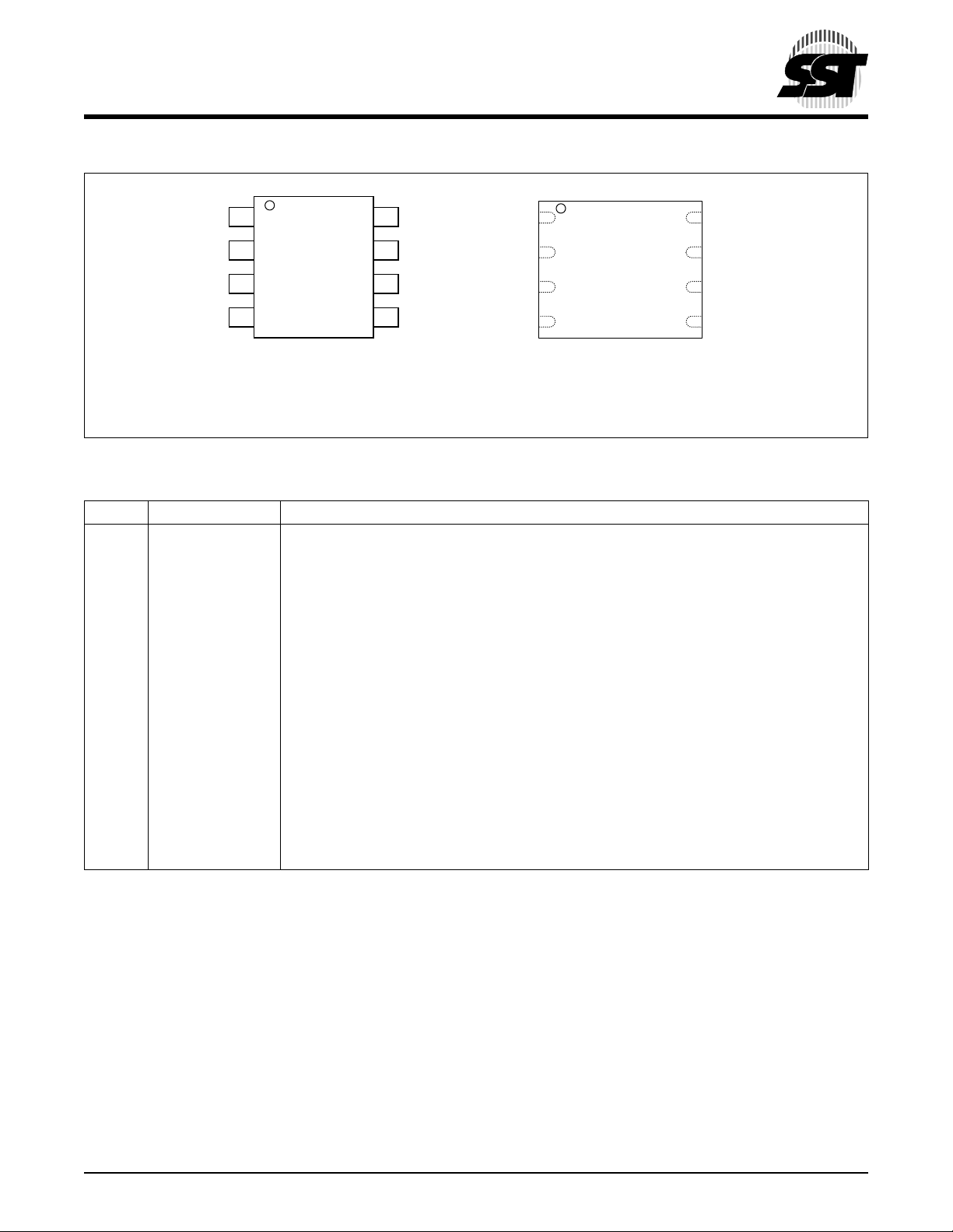
The SST45LF 010 device is offered in both 8- lead SOIC
and 8-contact WSON packages. See Figure 1 for the
pinouts.
Device Operation
The SST45LF01 0 uses bus cy cle s of 8 b its each for commands, data, and addresses to execute operations. The
operation instructions are listed in Tab le 3.
All instructions ar e syn chr onized off a high to low transiti on
of CE#. The first low to high trans ition on SCK will initiate
the instruction se quence. Inputs wil l be accep ted on the rising edge of SCK s tar ting with the m ost si gnificant bit. Any
low to high transition on CE# before the input instru ction
completes will terminate any instruction in progress and
return the device to the standby mode.
©2001 Silicon Storage Technology, Inc.
S71128-03-000 4/01 372
1
Sector/Chip-Erase Operation
The Sector-Erase op eration clears all bits in the se lected
sector to FFH. The Chip-Erase instruction clears all bits in
the device to FFH.
Byte-Program Operation
The Byte-Program operation programs the bits in the
selected byte to the desi red data. The s elected byte must
be in the erased state (FFH) when initiating a Program
operation. The data is input from bit 7 to bit 0 in order.
Software Status Operation
The Status opera tion determines if an Erase or Program
operation is in progress. If bit 0 is at a “0” an Erase or Pro-
gram operation is in progres s, the device is busy. If bit 0 is
at a “1” the device is ready for any valid operation. The sta-
tus read is cont inuous with ong oing cloc k cycles un til terminated by a low to high tran sition on CE#.
The SST logo and SuperFlash are registered trademarks of Silicon Storage Technology, Inc.
These specifications are subject to change without notice.
1 Megabit Serial Flash
SST45LF010
Data Sheet
Reset
Reset will terminate any oper ation, e .g., Re ad, Erase and
Program, in prog re ss . It is a ctivated by a hi gh to lo w t ra nsition on t he RST# pin. Th e device will rema in in reset
condition as long as RS T# is low. Minimum res et time is
10 µs. See Figur e 14 for reset timing diagram. RST# is
internally pulled-up and could remain unconnected during normal operation. Af ter re set, the d evice is in stan dby
mode, a high to low transition on CE# is required to start
the next oper ation .
An internal power-on reset circuit protects against accidental data writes. Appl ying a logic le vel lo w to RST# during the power-on process then changing to a logic level
high when V
has reached the correct voltage level will
DD
provide additional protection against accidental writes
during powe r on .
Read SST ID/Read Device ID
The Read SST ID and Read Device ID operations read the
JEDEC assigned manufacturer identification and the manufacturer assigned device identification IDs. These IDs may be
used to determine the actual device resident in the system.
TABLE 1: P
Manufacturer’s ID 0000H BFH
Device ID 0001H 42H
RODUCT IDENTIFICATION
Byte Data
T1.2 372
Write Protect
The WP# pin provides inadvertent write protection. The
WP# pin must be held high for any Erase or Program operation. The WP# pin is “Don’t Care” for all other operations.
In typical use, the WP# pin is connected to V
dard pull-down resistor. WP# is then driven high whenever
an Erase or Program operation i s requi red. If the W P# pi n
is tied to V
with a pull-up resistor, then all operations may
DD
occur and the write protection feature is disabled. The WP#
pin has an inter nal pu ll-up and could r emain un connecte d
when not use d.
with a stan-
SS
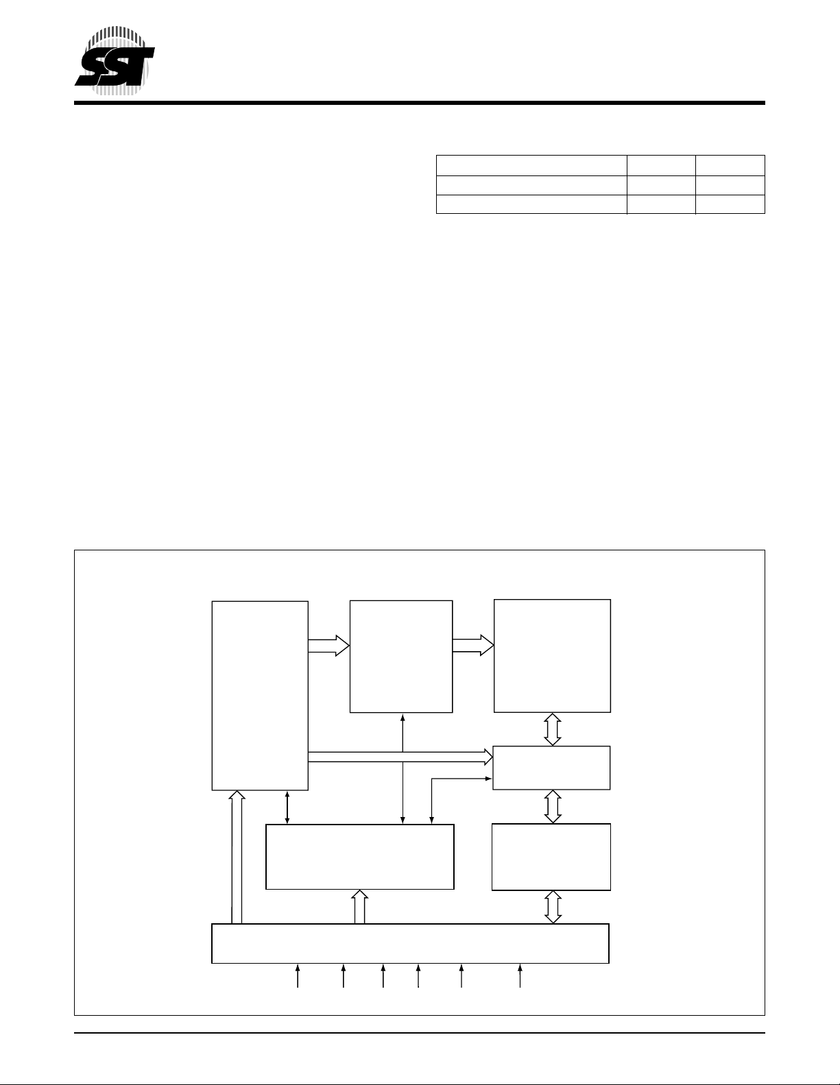
FUNCTIONAL BLOCK DIAGRAM
Address
Buffers
and
Latches
X - Decoder
Control Logic
Serial Interface
SuperFlash
Memory
Y - Decoder
I/O Buffers
and
Data Latches
CE#
©2001 Silicon Storage Technology, Inc. S71128-03-000 4/01 372
SCK SI SO WP# RST#
2
372 ILL B1.4
1 Megabit Serial Flash
SST45LF010
Data Sheet
WP#
V
DD
CE#
SCK
1
2
T op Vie w
3
4
8
RST#
7
V
6
SO
5
SI
372 ILL F01.6
SS
WP#
V
DD
CE#
SCK
1
2
T op View
3
4
8
RST#
7
V
SS
6
SO
5
SI
372 ILL F01a.2
8-LEAD SOIC 8-CONTACT WSON
FIGURE 1: PIN ASSIGNMENTS
TABLE 2: PIN DESCRIPTION
Symbol Pin Name Functions
SCK Serial Clock To provide the timing of the serial interface. Commands, addresses, or input data are latched
on the rising edge of the clock input, while output data is shifted out on the falling edge of the
clock input.
SI Serial Data Input To transfer commands, addresses, or data serially into the device. Inputs are latched on the
rising edge of the serial clock.
SO Serial Data Output To transfer data serially out of the device.
Data is shifted out on the falling edge of the serial clock.
CE# Chip Enable The device is enabled by a high to low transition on CE#.
WP# Write Protect To protect the device from unintentional Write (Erase or Program) operations. When WP# is
low, all Erase and Program commands are ignored. When WP# is high, the device may be
erased or programmed. This pin has an internal pull-up and could remain unconnected when
not used.
RST# Reset A high to low tra nsitio n on RST# will te rminate an y o per ation in p rogre ss an d res et the internal
logic to the stand by mod e. T he de v ice wi ll remain in the reset condi tion as long as the RST# is
low. Operations may only occ ur w h en RS T # is hi gh. This pin has an int ernal p ull -up and co uld
remain unconnected when not used.
V
DD
V
SS
Power Supply To provide power supply (3.0-3.6V).
Ground
T2.5 372
©2001 Silicon Storage Technology, Inc. S71128-03-000 4/01 372
3
1 Megabit Serial Flash
SST45LF010
Data Sheet
OUT
1
S
S
IN
OUT
S
S
IN
OUTSINSOUTSINSOUTSINSOUT
Hi-Z X Hi-Z X Hi-Z X D
0
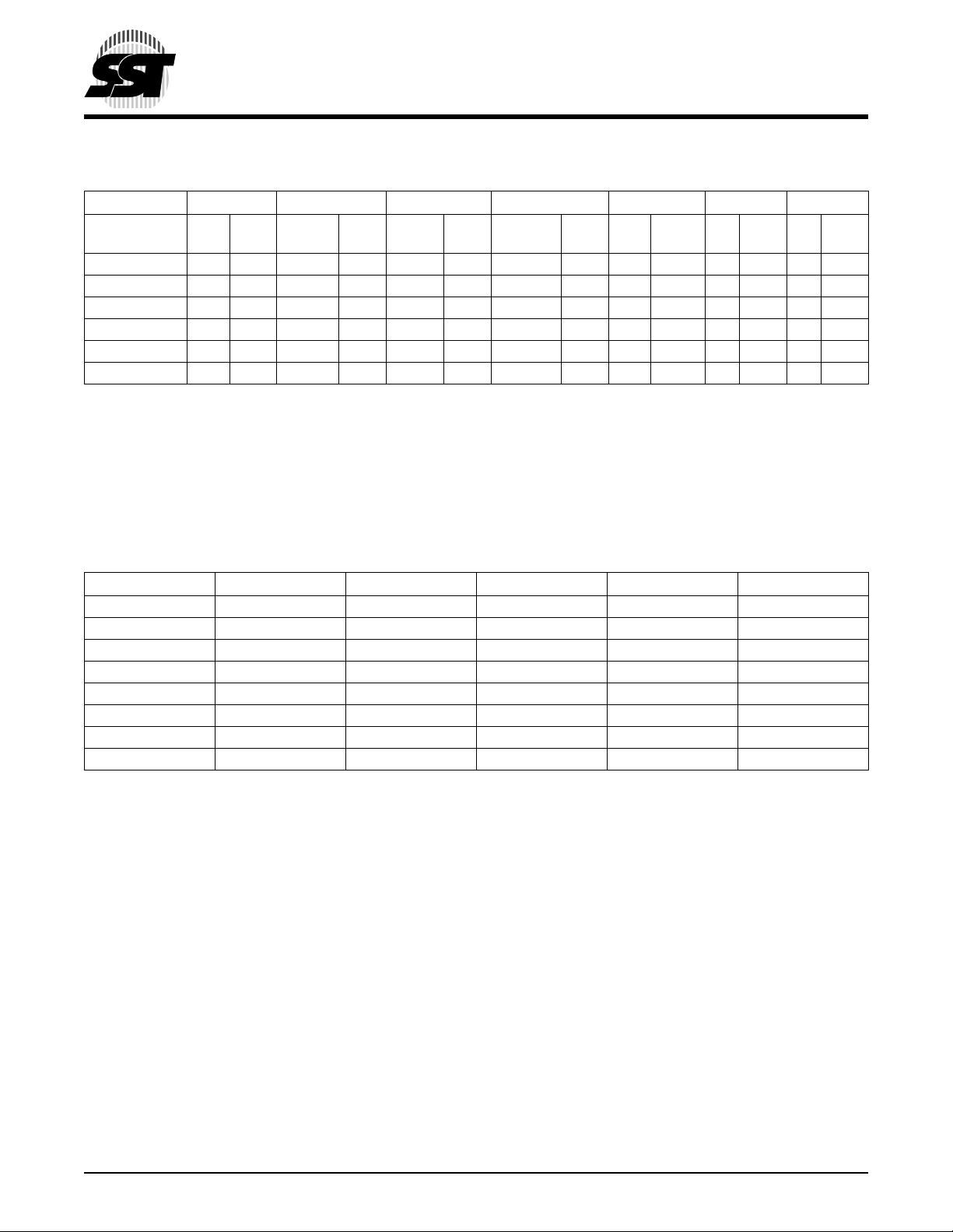
TABLE 3: DEVICE OPERATION INSTRUCTIONS
Bus Cycle
Cycle Type/
Operation
Read FFH Hi-Z A23-A16Hi-Z A15-A8Hi-Z A7-A
Sector-Erase
2
3,4
5
12 3 4 567
SINS
OUT
S
S
IN
20H Hi-Z A23-A16Hi-Z A15-A8Hi-Z X Hi-Z D0H Hi-Z X Hi-Z X Hi-Z
Chip-Erase 60H Hi -Z X Hi-Z X Hi-Z X Hi-Z D0H Hi-Z X Hi-Z X Hi-Z
Byte-Program 10H Hi-Z A
23-A16
Status Reg. 9FH X X D
Hi-Z A15-A8Hi-Z A7-A
6
Note
OUT
X
X Note6X Note6X Note6X Note
Read-ID 90H Hi-Z 00H Hi-Z 00H Hi-Z ID Addr
1. For SST45LF010, A23-A17 are “Don’t Care.”
2. One bus cycle is eight clock periods
3. Operation: SIN=Serial In, S
4. X=D ummy cycles (Don’t Care)
5. A16-A12 are used to determine sector address, A11-A8 are “Don’t Care.”
6. The status read is continuous with ongoing clock cycles until terminated by a low to high transition on CE#.
7. Manufacturer’s ID=BFH, is read with A0 =0 and Device ID = 42H, is read with A0 =1; All other address bits are 0
8. The data output is arbitrary.
=Serial Out
OUT
Hi-Z D
0
7
Hi-Z X D
Hi-Z X Hi-Z X Hi-Z
IN
OUT
7
X Note
8
X Note
T3.10 372
TABLE 4: DEVICE OPERATION TABLE
Operation SI SO CE#
Read X D
OUT
Sector-Erase X X Low High High
Chip-Erase X X Low High High
Byte-Program D
IN
Software-Status X D
2
Reset
XXXXLow
Read SST ID X D
Read Device ID X D
1. A high to low transition on CE# will be required to start any device operation except for Reset.
2. The RST# low will return the device to standby and terminate any Erase or Program operation in progress.
X Low High High
OUT
OUT
OUT
1
WP# RST#
Low X High
Low X High
Low X High
Low X High
T4.6 372
OUT
6
8
©2001 Silicon Storage Technology, Inc. S71128-03-000 4/01 372
4

1 Megabit Serial Flash
SST45LF010
Data Sheet
Absolute Maximum Stress Ratings (Applied conditions greater than those listed under “Absolute Maximum
Stress Ratings” may cause pe r manent dama ge to the device. This is a stres s rating only and funct ional operatio n
of the device at these conditions or conditions greater tha n those defined in the ope rational sections of this data
sheet is not implied. Exposure to absolute maximum stress rating conditions may affect device reliability.)
Temperature Under Bias . . . . . . . . . . . . . . . . . . . . . . . . . . . . . . . . . . . . . . . . . . . . . . . . . . . . . . . . . -55°C to +125°C
Storage Temperature . . . . . . . . . . . . . . . . . . . . . . . . . . . . . . . . . . . . . . . . . . . . . . . . . . . . . . . . . . . . -65°C to +150°C
D. C. Voltage on Any Pin to Ground Potential . . . . . . . . . . . . . . . . . . . . . . . . . . . . . . . . . . . . . . . .-0.5V to V
Transient Voltage (<20 ns) on Any Pin to Ground Potential . . . . . . . . . . . . . . . . . . . . . . . . . . . . . .-1.0V to V
Package Power Dissipation Capability (Ta = 25°C) . . . . . . . . . . . . . . . . . . . . . . . . . . . . . . . . . . . . . . . . . . . . . . 1.0W
Surface Mount Lead Soldering Temperature (3 Seconds). . . . . . . . . . . . . . . . . . . . . . . . . . . . . . . . . . . . . . . . 240°C
1
Output Short Circ uit Curr ent
1. Outputs shorted for no more than one second. No more than one output shorted at a time.
. . . . . . . . . . . . . . . . . . . . . . . . . . . . . . . . . . . . . . . . . . . . . . . . . . . . . . . . . . . . . . 50 mA
DD
DD
+0.5V
+1.0V
OPERATING RANGE
Range Ambient Temp V
Commercial 0°C to +70°C3.3V±0.3V
DD
AC CONDITIONS OF TEST
Input Rise/Fall Time . . . . . . . . . . . . . . . 5 ns
Output Load . . . . . . . . . . . . . . . . . . . . . CL = 30 pF
See Figures 2 and 3
TABLE 5: DC OPERATING CHARACTERISTICS VDD = 3.0-3.6V
Limits
Symbol Parameter
I
DD
I
SB
I
LI
I
LO
I
IL
V
IL
V
IH
V
IHC
V
OL
V
OH
1. This parameter only applies to WP# and RST# pins.
Power Supply Current f=10 MHz
Read 20 mA CE#=V
Program and Erase 30 mA CE#=VIL, VDD=VDD Max
Standby Current 15 µA CE#=V
Input Leakage Current 1 µA VIN=GND to VDD, VDD=VDD Max
Output Leakage Current 1 µA V
Input Low Current
1
360 µA WP#, RST#=GND
Input Low Voltage 0.8 V VDD=VDD Min
Input High Voltage 0.7 V
DD
Input High Voltage (CMOS) VDD-0.3 V VDD=VDD Max
Output Low Voltage 0.2 V IOL=100 µA, VDD=VDD Min
Output High Voltage VDD-0.2 V IOH=-100 µA, VDD=VDD Min
Test ConditionsMin Max Units
, VDD=VDD Max
IL
, VDD=VDD Max
IHC
=GND to VDD, VDD=VDD Max
OUT
VVDD=VDD Max
T5.1 372
©2001 Silicon Storage Technology, Inc. S71128-03-000 4/01 372
5
 Loading...