

Silicon Storage Technology Inc SST39VF160-90-4I-EK, SST39VF160-90-4C-EK, SST39VF160-90-4C-B3K, SST39VF160-70-4I-EK, SST39VF160-70-4I-B3K Datasheet
...
FEATURES:
16 Mbit (x16) Multi-Purpose Flash
SST39LF160 / SST39VF160
SST39LF/VF1603.0 & 2.7V 16Mb (x16) MPF memories
Data Sheet
• Organized as 1M x16
• Single Voltage Read and Write Operations
– 3.0-3.6V for SST39LF160
– 2.7-3.6V for SST39VF160
• Superior Reliability
– Endurance: 100,000 Cycles (typical)
– Greater than 100 years Data Retention
• Low Power Consumption
– Ac ti ve Current: 15 mA (typical)
– Standby Current: 4 µA (typical)
– Auto Low Power Mode: 4 µA (typical)
• Sector-Erase Capability
– Uniform 2 KWord sectors
• Fast Read Access Time
– 55 ns for SST39LF160
– 70 and 90 ns for SST39VF160
• Latched Address and Data
PRODUCT DESCRIPTION
The SST39LF/VF160 devices are 1M x16 CMOS MultiPurpose Flash (MPF) manufactured with SST’s proprietary ,
high performance CMOS SuperFlash technology. The
split-gate cell design and thick oxide tunneling injector
attain better reliability and manufacturability compared with
alternate approaches. The SST39LF160 write (Program or
Erase) with a 3.0-3.6V power supply. The SST39VF160
write (Program or Erase) with a 2.7-3.6V power supply.
These devices conform to JEDEC standard pinouts for x16
memories.
Featuring high performance Word-Program, the SST39LF/
VF160 devices provide a typical Word-Program time of 14
µsec.These devices use Toggle Bit or Data# Polling to indicate the completion of Program operation. To protect
against inadver ten t wri te, they have on-chip hardware an d
Software Data Protection schemes. Designed, manufactured, and tested for a wide spectrum of applications, these
devices are offered with a guaranteed endurance of 10,000
cycles. Data retention is rated at greater than 100 years.
The SST39LF/VF160 devices are suited for applications
that require convenient and economical updating of program, configuration, or data memory. For all system applications, they significantly improve performance and
reliability, while lowering power consumptio n. They inherently use less energy during Erase and Program than alternative flash technologi es. The total energy consu med is a
function of the applied voltage, current, and time of application. Since for any given voltage range, the SuperFlash
• Fast Erase and Word-Program
– Sector-Erase Time: 18 ms (typical)
– Block-Erase Time: 18 ms (typical)
– Chip-Erase Time: 70 ms (typical)
– Word-Program Time: 14 µs (typical)
– Chip Rewrite Time: 15 seconds (typical) for
SST39LF/VF160
• Automatic Write Timing
– Internal V
Generation
PP
• End-of-Write Detection
– Toggle Bit
– Data# Polling
• CMOS I/O Compatibility
• JEDEC Standard
– Flash EEPROM Pinouts and command sets
• Packages Available
– 48-lead TSOP (12mm x 20mm)
– 48-ball TFBGA (6mm x 8mm)
technology uses less current to program and has a shorter
erase time, the total energy consumed during any Erase or
Program operation is l ess than alter native flash technologies. These devices also im prove flexibility while lowering
the cost for program, data, and configuration storage applications.
The SuperFlash te ch nology provides fixed Erase and P r ogram times, independent o f th e numbe r of Erase/ Pro gram
cycles that have occurred. Therefore the system software
or hardware does not have to be modified or de-rated as is
necessary with alternative flash technologies, whose Erase
and Program times i ncrease with accumul ated Erase/P rogram cycles .
To meet high density, surface mount requirements, the
SST39LF/VF160 ar e offered in 48-lead TSOP and 48- ball
TFBGA packages. See Figure 1 for pinouts.
Device Operation
Commands are used to initiate the memory operation functions of the device. Commands ar e written to the device
using standard microprocess or write sequences. A command is written by asse r ting WE# low whil e keeping CE#
low. The address bus is latched on the falling edge of WE#
or CE#, whichever occurs last. T he data bus is latc hed o n
the rising edge of WE# or CE#, whichever occurs first.
©2001 Silicon Storage Technology, Inc.
S71145-02-000 6/01 399
1
The SST logo and SuperFlash are registered trademarks of Silicon Storage Technology, Inc.
MPF is a trademark of Silicon Storage Technology, Inc.
These specifications are subject to change without notice.

16 Mbit Multi-Purpose Flash
SST39LF160 / SST39VF160
Data Sheet
The SST39LF/VF160 also have the Auto Low Power
mode which puts the device in a ne ar standby mode aft er
data has been accessed with a valid Read operation. This
reduces the I
typically 4 µA. The Auto Low Pow er mode reduces the typi-
active read current to the range of 1 mA/MHz of
cal I
DD
read cycle time. The device exits the Auto Low Power
mode with any address transition or control signal transition
used to initiate ano ther Read cycle, with no access t ime
penalty. Note that the device does not enter Auto Low
Po wer m ode afte r po wer-up with CE # held s teadily low u ntil
the first add ress tr ansi tion or CE# is driv en hi gh.
active read current from typically 15 mA to
DD
Read
The Read operation of the SST39LF/VF160 is controlled
by CE# and OE#, both h ave to be low for the system to
obtain data from the outputs. CE# is used for device selection. When CE# is high, the chip is desele cted and only
standby power is consumed. OE# is the output control and
is used to gate data from the output pins. The data bus is in
high impedance state when either CE# or OE# is high.
Refer to the Read cycle timing diagram for fur ther details
(Figure 2).
Word-Program Operation
The SST39LF/VF160 are programmed on a word-by-word
basis. Before programming, one must ensure that the sector, in which the word which is being programmed exists, is
fully erased. The Program operation consists of three
steps. The first step is the three-byte load sequence for
Software Data Protection. The second step is to load word
address and word data . During t he Word-Program operation, the addresses are latched on the falling edge of either
CE# or WE#, whichever occurs last. The data is latched on
the rising edg e of either CE# or WE#, whichever occurs
first. The third step is the internal Program operation which
is initiated afte r the r ising e dge of th e four th WE# or CE#,
whichever occurs first. The P rogram operation, once in itiated, will be comple ted with in 20 µs. See Figu res 3 and 4
for WE# and CE# controlled Program operation timing diagrams and Figure 15 for flowcharts. During the Program
operation, the only valid reads are Data# Polling and Toggle Bit. During the in ternal Program opera tion, the host is
free to perform additional tasks. Any commands issued
during the internal Program operation are ignored.
Sector/Block-Erase Operation
The Sector- (or Block-) Erase operation allows the system
to erase the device on a sector-by-sector (or block-byblock) basis. The SST39LF/VF160 offer both Sector-Erase
and Block-Erase mode. The sec tor architecture is based
on unifo rm sector si z e of 2 KWord. The Blo ck-Erase mo de
is based on unifor m block size of 32 KWord. The SectorErase operation is initiated by executing a six-byte command sequence with Sector-Erase command (30H) and
sector address (SA) in the last bus cycle. The Block-Erase
operation is initiated by executing a six-byte command
sequence with Block-Erase command (50H) and block
address (BA) in the last bus cycle. The sector or block
address is latched on the falling edge of the sixth WE#
pulse, while the comm and (30H or 50H) is latched on th e
rising edge of the sixth WE# pulse. The internal Erase
operation begins a fter the sixth WE# pulse. The End -ofErase operation can be determined using either Data#
Polling or Toggle Bit methods. See Figures 8 and 9 for timing waveforms. Any commands issued d uring the Sectoror Block-Erase operation are ignored.
Chip-Erase Operation
The SST39LF/VF160 provide a Chip-Erase operation,
which allows the user to erase the en tire mem ory array to
the “1” state. This is useful when the entire device must be
quickly erased.
The Chip-Erase operation is initiated by executing a sixbyte command sequence with Chip-Erase command (10H)
at address 5555H in the last byte sequence. The Eras e
operation begins with the rising edge of the sixt h WE# or
CE#, whichever occurs first. During the Erase operation,
the only valid read is T oggle Bit or Data# Polling. See Table
4 for the command sequence, Figure 7 for timing diagram,
and Figure 18 for the flowchart. Any commands issued during the Chip-Erase operation are ignored.
Write Operation Status Detection
The SST39LF/VF160 provide two software means to
detect the completion of a Write (Program or Erase) cycle,
in order to opt imize the system wr ite cy cle time. Th e software detection includes two status bits: Data# Polling
) and Toggle Bit (DQ6). The End-of-Write detection
(DQ
7
mode is enabled after the r ising edge of WE#, which in itiates the internal Program or Erase operation.
The actual comple tion of the n onvolatile write is as ync hronous with the sys tem; therefore, either a Data# Polling or
Toggle Bit read may be simultaneous wi th the complet ion
of the write cycle. If this occurs, the system may possibly
get an erroneous result, i.e., valid data may appear to conflict with either DQ
rejection, if an erroneous result occurs, the software routine
should include a loop to read the accessed location an
additional two (2) times. If bo th reads are valid, then the
device has completed the Write cycle, otherwise the rejection is valid.
or DQ6. In order to prevent spurious
7
©2001 Silicon Storage Technology, Inc. S71145-02-000 6/01 399
2
16 Mbit Multi-Purpose Flash
SST39LF160 / SST39VF160
Data Sheet
Data# Polling (DQ7)
When the SST39LF/VF160 are in the internal Program
operation, any attemp t to read DQ
will produce the com-
7
plement of the tru e data. Once the Program operation is
completed, DQ
will produce true data. T he device is then
7
ready for the next operation. Dur ing inter nal Erase ope ration, any attempt to read DQ
internal Erase operation is compl eted, DQ
will produce a ‘0’. Once the
7
will produce a
7
‘1’. The Data# Polling is valid after the rising edge of fourth
WE# (or CE#) pulse for Program operat ion. For Sector-,
Block- or Chip-Erase, the Data# Polling is valid after the rising edge of sixth WE # (or CE#) pulse. See Figure 5 for
Data# Polling timing diagram and Figure 16 for a flowchart.
Toggle Bit (DQ6)
During the inter nal Program or Erase ope ration, any consecutive attempts to read DQ
will produce alter nating 1s
6
and 0s, i.e., toggling between 1 and 0. W hen the internal
Program or Erase operat ion is complete d, the DQ
bit will
6
stop toggling. The device is the n re ady for the next ope ration. The Toggle Bit is valid af ter the rising edge of fourth
WE# (or CE#) pulse for Program operat ion. For Sector-,
Block- or Chip-Erase, the Toggle Bit is valid after the risin g
edge of sixth WE# (or CE#) pulse. See Figure 6 for Toggle
Bit timing diag ram and Fi gure 16 f or a fl owc hart.
Data Protection
The SST39LF/VF160 provide both hardware and software
features to protect nonvolatile data from inadvertent writes.
Hardware Data Protection
Noise/Glitch Protection: A WE# or CE# pulse of le ss than 5
ns will not initiate a write cycle.
Power Up/Down Detection: The Write operation is
V
DD
inhibited when V
Write Inhibit Mode:
is less than 1.5V.
DD
Forcing OE# low, CE# high, or WE#
high will inhibit the W r ite operation. This prevents inadvertent writes durin g pow er-u p or po wer- dow n.
Software Data Protection (SDP)
The SST39LF/VF160 provide the JEDEC approved Software Data Protection s che me for all da ta al teration operations, i.e., Program and Erase. Any Program operation
requires the inclusion of the three-byte sequence. The
three-byte load sequ ence is used to initiate the Pro gram
operation, providing optimal protection from inadvertent
Write operations, e.g., during the system power-up or
power-d own. Any Er as e o peration requi re s th e incl usion of
six-byte sequence. These devices are shipped with the
Software Data Protectio n pe rmanently ena bled. Se e Table
4 for the specific software co mmand codes. During SDP
command sequence, invalid commands will abort the
device to read mode within T
can be VIL or VIH, but no other value, during any SDP command sequence.
. The contents of DQ15-DQ
RC
8
©2001 Silicon Storage Technology, Inc. S71145-02-000 6/01 399
3
16 Mbit Multi-Purpose Flash
SST39LF160 / SST39VF160
Data Sheet
Common Flash Memory Interface (CFI)
The SST39LF160 and SST39VF160 also contain the CFI
information to descr ibe the characteristics of the device.
In order to enter the CFI Query mode, the system must
write three-byte sequence, same as product ID entry
command with 98H (CFI Query command) to address
5555H in the last byte sequence. Once t he device ent ers
the CFI Query mode, the system can read CFI data at the
addresses given in Tables 5 through 7. The system must
write the CFI Exit command to return to Read mode from
the CFI Query mode.
Product Identification
The Product Id entification mode ide ntifies the devices as
the SST39LF/VF160 and manufacturer as SST. This mode
may be accessed by software ope rations. Users m ay use
the Software Product Ident ifi c ati on operati on to id en tify the
part (i. e., using the device ID) when usi ng multiple manufacturers in the same socket. For details, see Table 4 for
software operation, Figure 10 for the Software ID Entry and
Read timing diagram, and Figure 17 for the Software ID
Entry command sequenc e flow chart.
TABLE 1: P
Manufacturer’s ID 0000H 00BFH
Device ID
SST39LF/VF160 0001H 2782H
RODUCT IDENTIFICATION
Address Data
T1.2 399
Product Identification Mode Exit/
CFI Mode Exit
In order to return to the standard Read mode, the Software
Product Identific ation mode must be exited. Exit is acco mplished by issuing the Software ID Exit command
sequence, which returns the device to the Read operation.
This command may also be used to reset the device to the
Read mode after any inadvertent transient condition that
apparently caus es the device to behave abnor mally, e.g.,
not read correct ly. Please note that the Software ID Exit /
CFI Exit command is ignored during an internal Program or
Erase operation. See Table 4 for software command
codes, Figure 12 for timing waveform and Figure 17 for a
flowchart.
©2001 Silicon Storage Technology, Inc. S71145-02-000 6/01 399
4
16 Mbit Multi-Purpose Flash
SST39LF160 / SST39VF160
Data Sheet
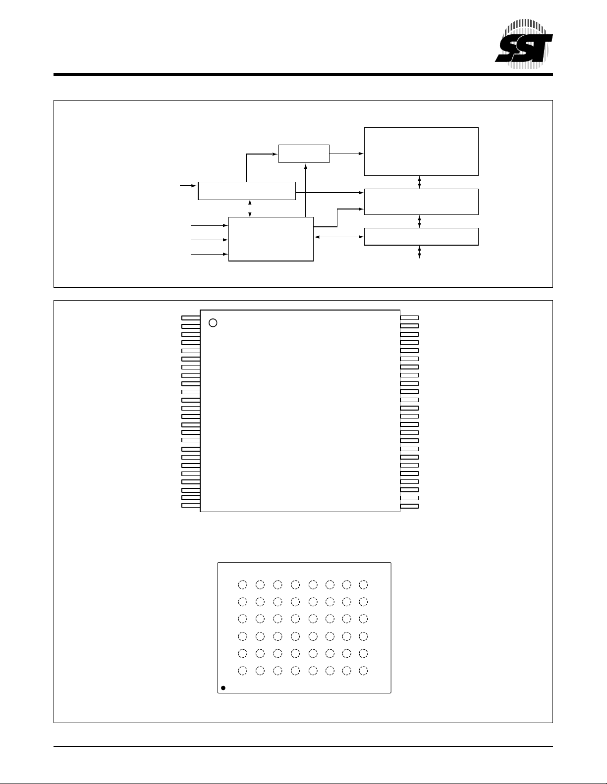
FUNCTIONAL BLOCK DIAGRAM
Memory Address
A15
A14
A13
A12
A11
A10
A19
WE#
A18
A17
Address Buffer & Latches
CE#
OE#
WE#
1
2
3
4
5
A9
A8
NC
NC
NC
NC
NC
A7
A6
A5
A4
A3
A2
A1
6
7
8
9
10
11
12
13
14
15
16
17
18
19
20
21
22
23
24
X-Decoder
Control Logic
Standard Pinout
T op Vie w
Die Up
SST39LF160/SST39VF160
SuperFlash
Memory
Y-Decoder
I/O Buffers and Data Latches
DQ15 - DQ
48
47
46
45
44
43
42
41
40
39
38
37
36
35
34
33
32
31
30
29
28
27
26
25
399 ILL F01.2
A16
NC
V
SS
DQ15
DQ7
DQ14
DQ6
DQ13
DQ5
DQ12
DQ4
V
DD
DQ11
DQ3
DQ10
DQ2
DQ9
DQ1
DQ8
DQ0
OE#
V
SS
CE#
A0
0
399 ILL B1.1
TOP VIEW (balls facing down)
SST39LF/VF160
6
A13
A12
A14
A15
A16
NC
DQ15
V
SS
5
4
3
2
1
A9
WE#
NC
A7
A3
A8
NC
NC
A17
A4
A10
NC
A18
A6
A2
A11
A19
NC
A5
A1
DQ7
DQ5
DQ2
DQ0
A0
DQ14
DQ12
DQ10
DQ8
CE#
DQ13
V
DD
DQ11
DQ9
OE#
DQ6
DQ4
DQ3
DQ1
V
SS
399 ILL F02a.1
A B C D E F G H
FIGURE 1: PIN ASSIGNME NTS FOR 48-LEA D TSOP AND 48-BALL TFBGA
©2001 Silicon Storage Technology, Inc. S71145-02-000 6/01 399
5
16 Mbit Multi-Purpose Flash
SST39LF160 / SST39VF160
TABLE 2: PIN DESCRIPTION
Symbol Pin Name Functions
A
19-A0
-DQ
DQ
15
CE# Chip Enable To activate the device when CE# is low
OE# Output Enable To gate the data output buffers
WE# Write Enable To control the Write operations
V
DD
V
SS
NC No Connection Unconnected pins
TABLE 3: OPERATION MODES SELECTION
Mode CE# OE# WE# DQ Address
Read V
Program V
Erase V
Standby V
Write Inhibit X V
Product Identification
Software Mode V
1. X can be VIL or VIH, but no other value
Address Inputs To provide memory addresses. During Sector-Erase A19-A11 address lines will select the
sector. During Block-Erase, A
Data Input/output To output data during Read cycles and receive input data during Write cycles.
0
address line will select the block.
19-A15
Data is internally latched during a Write cycle.
The outputs are in tri-state when OE# or CE# is high.
Power Supply To provide power supply voltage: 3.0-3.6V for SST39LF160
2.7-3.6V for SST39VF160
Ground
IL
IL
IL
V
IL
V
IH
V
IH
V
V
V
D
IH
IL
IL
OUT
D
IN
1
X
A
IN
A
IN
Sector or B lock address,
XXH for Chip-Erase
IH
XXVIHHigh Z/ D
IL
XXHigh Z X
IL
V
IL
XHigh Z/ D
V
IH
OUT
OUT
X
X
See Table 4
Data Sheet
T2.3 399
T3.4 399
©2001 Silicon Storage Technology, Inc. S71145-02-000 6/01 399
6
16 Mbit Multi-Purpose Flash
SST39LF160 / SST39VF160
Data Sheet
TABLE 4: SOFTWARE COMMAND SEQUENCE
Command
Sequence
Word-Program 5555H AAH 2AAAH 55H 5555H A0H WA3Data
Sector-Erase 5555H AAH 2AAAH 55H 5555H 80H 5555H AAH 2AAAH 55H SA
Block-Erase 5555H AAH 2AAAH 55H 5555H 80H 5555H AAH 2AAAH 55H BA
Chip-Erase 5555H AAH 2AAAH 55H 5555H 80H 5555H AAH 2AAAH 55H 5555H 10H
Software ID Entry
CFI Query Entry
Software ID Exit
5,6
5
7
/
CFI Exit
Software ID Exit
7
/
CFI Exit
1. Addres s format A14-A0 (Hex), Addres ses A15-A19 can be VIL or VIH, but no other value, f or Command sequence for SST39LF/VF160
- DQ8 can be VIL or VIH, but no other value, for Command sequence
2. DQ
15
3. WA = Program word address
for Sector-Erase; uses A19-A11 address lines
4. SA
X
BA
, for Block-Erase; uses A19-A15 address lines
X
5. The device does not remain in Software Product ID Mode if powered down.
6. With A
7. Both Software ID Exit operations are equivalent
=0; SST Manufacturer’s ID= 00BFH, is read with A0 = 0,
19-A1
1st Bus
Write Cycle
2nd Bus
Write Cycle
3rd Bus
Write Cycle
4th Bus
Write Cycle
5th Bus
Write Cycle
6th Bus
Write Cycle
Addr1Data2Addr1Data2Addr1Data2Addr1Data2Addr1Data2Addr1Data
4
X
4
X
5555H AAH 2AAAH 55H 5555H 90H
5555H AAH 2AAAH 55H 5555H 98H
XXH F0H
5555H AAH 2AAAH 55H 5555H F0H
SST39LF160/SST39VF160 Device ID = 2782H, is read with A
0
= 1
30H
50H
T4.4 399
2
TABLE 5: CFI QUERY IDENTIFICATION STRING1 FOR SST39LF /VF160
Address Data Data
10H 0051H Query Unique ASCII string “QRY”
11H 0052H
12H 0059H
13H 0001H Primary OEM command set
14H 0007H
15H 0000H Address for Primary Extended Table
16H 0000H
17H 0000H Alternate OEM command set (00H = none exists)
18H 0000H
19H 0000H Address for Alternate OEM extended Table (00H = none exits)
1AH 0000H
1. Refer to CFI publication 100 for more details.
T5.0 399
©2001 Silicon Storage Technology, Inc. S71145-02-000 6/01 399
7
16 Mbit Multi-Purpose Flash
SST39LF160 / SST39VF160
TABLE 6: SYSTEM INTERFACE INFORMATION FOR SST39LF/V F16 0
Address Data Data
1
1BH 0027H
0030H1DQ7-DQ4: Volts, DQ3-DQ0: 100 millivolts
1CH 0036H V
1DH 0000H V
1EH 0000H V
1FH 0004H Typical time out for Word-Prog ra m 2
20H 0000H Typical time out for min. size buffer program 2
21H 0004H Typical time out for ind ividu al Sec tor/Bl ock-Erase 2
22H 0006H Typical time out for C hip -Er ase 2
23H 0001H Maximum time out for Word-Program 2N times typical (21 x 24 = 32 µs)
24H 0000H Maximum time out for buffer program 2N times typical
25H 0001H Maximum time out for individual Sector/Block-Erase 2
26H 0001H Maximum time out for Chip-Erase 2N times typical (21 x 26 = 128 ms)
1. 0030H for SST39LF160 and 0027H for SST39VF160
VDD Min. (Program/Erase)
Max. (Program/Erase)
DD
DQ
-DQ4: Volts, DQ3-DQ0: 100 millivolts
7
min. (00H = no VPP pin)
PP
max. (00H = no VPP pin)
PP
N
µs (24 = 16 µs)
N
N
ms (26 = 64 ms)
µs (00H = not supported)
N
ms (24 = 16 ms)
N
times typica l (21 x 24 = 32 ms)
Data Sheet
T6.2 399
TABLE 7: DEVICE GEOMETRY INFORMATION FOR SST39LF/VF160
Address Data Data
27H 0015H Device size = 2
28H 0001H Flash Device Interface description; 0001H = x16-only asynchronous interface
29H 0000H
2AH 0000H Maximum number of bytes in multi-byte write = 2
2BH 0000H
2CH 0002H Number of Erase Sector/Block sizes supported by device
2DH 00FFH Sector Information (y + 1 = Number of sectors; z x 256B = sector size)
2EH 0001H y = 155 + 1 = 512 sectors (01FFH = 511)
2FH 0010H
30H 0000H z = 16 x 256 Bytes = 4 KBytes/sector (0010H = 16)
31H 003FH Block Information (y + 1 = Number of blocks; z x 256B = block size)
32H 0000H y = 31 + 1 = 32 blocks (001FH = 31)
33H 0000H
34H 0001H z = 256 x 256 Bytes = 64 KBytes/block (0100H = 256)
N
Bytes (15H = 21; 221 = 2 MBytes)
N
(00H = not supported)
T7.3 399
©2001 Silicon Storage Technology, Inc. S71145-02-000 6/01 399
8
 Loading...