

Silicon Storage Technology Inc SST39VF100-70-4I-WK, SST39VF100-70-4I-WI, SST39VF100-70-4I-B3K, SST39VF100-70-4I-B3I, SST39VF100-70-4C-WK Datasheet
...
FEATURES:
1 Mbit (64K x16) Multi-Purpose Flash
SST39LF100 / SST39VF100
SST39LF/VF1003.0 & 2.7V 1 Mb (x16) MPF memories
Data Sheet
• Organized as 64K x16
• Single Voltage Read and Write Operations
– 3.0-3.6V for SST39LF100
– 2.7-3.6V for SST39VF100
• Superior Reliability
– Endurance: 100,000 Cycles (typical)
– Greater than 100 years Data Retention
• Low Power Consumption
– Ac ti ve Current: 20 mA (typical)
– Standby Current: 3 µA (typical)
• Sector-Erase Capability
– Uniform 2 KWord sectors
• Fast Read Access Time
– 45 ns for SST39LF100
– 70 ns for SST39VF100
• Latched Address and Data
PRODUCT DESCRIPTION
The SST39LF/VF 100 devices are 64K x16 CMOS MultiPurpose Flash (MPF) manufactured with SST’s proprietary ,
high performance CMOS SuperFlash technology. The
split-gate cell design and thick oxide tunneling injector
attain better reliability and manufacturability compared with
alternate approaches. The SST39LF100 and
SST39VF100 wr ite (Program or Erase) with a si ngle voltage power supply of 3.0-3.6V and 2.7-3.6V, respectively.
Featuring high performance Word-Program, the SST39LF/
VF100 devices provide a typical Word-Program time of 14
µsec. The de vice s use Toggle Bit or Data # P oll ing to dete ct
the completion of the Pr ogram or Erase o perati on. To protect against inadvertent write, the SST39LF/VF100 have
on-chip hardware and s oftware data protection schem es.
Designed, manufactured, and tested for a wide spectrum of
applications, the SST39 LF/VF10 0 are offered with a guaranteed endur a nce of 10 ,00 0 cycle s. Data r etent ion is ra ted
at greater than 100 years.
The SST39LF/VF100 devices are suited for applications
that require convenient and economical updating of program, configuration, or data memory. For all system applications, the SST39LF/VF100 significantly improve
performanc e and relia bility, while loweri ng powe r consumption. The SST39LF /VF100 inhe rent ly us e less ener gy during Erase and Program than alternative flash technologies.
The total energy consumed is a function of the applied voltage, current, and tim e of application. Si nce for any given
voltage range, the SuperFla sh technology uses less current to program and has a shorter erase time, the total
• Fast Erase and Word-Program
– Sector-Erase Time: 18 ms (typical)
– Chip-Erase Time: 70 ms (typical)
– Word-Program Time: 14 µs (typical)
– Chip Rewrite Time: 1 second (typical)
• Automatic Write Timing
– Internal V
Generation
PP
• End-of-Write Detection
– Toggle Bit
– Data# Polling
• CMOS I/O Compatibility
• JEDEC Standard Command Sets
• Packages Available
– 40-lead TSOP (10mm x 14mm)
– 48-ball TFBGA (6mm x 8mm)
energy consumed during any Erase or Program operation
is less than alternative flash technologies. The SST39LF/
VF100 also im prove flexibility while lowering the cost for
program, data, and configuration storage applications.
The SuperFlash te ch nology provides fixed Erase and P r ogram times, independent o f th e numbe r of Erase/ Pro gram
cycles that have occurred. Therefore the system software
or hardware does not have to be modified or de-rated as is
necessary with alternative flash technologies, whose Erase
and Program times i ncrease with accumul ated Erase/P rogram cycles .
To meet surface mount requirements, the SST39LF/VF100
are offered in 40-lead TSOP and 48-ball TFBGA packages.
See Figure 1 for pinout.
Device Operation
Commands are used to initiate the memory operation functions of the device. Commands ar e written to the device
using standard microprocess or write sequences. A command is written by asse r ting WE# low whil e keeping CE#
low. The address bus is latched on the falling edge of WE#
or CE#, whichever occurs last. T he data bus is latc hed o n
the rising edge of WE# or CE#, whichever occurs first.
©2001 Silicon Storage Technology, Inc.
S71129-02-000 6/01 363
1
The SST logo and SuperFlash are registered trademarks of Silicon Storage Technology, Inc.
MPF is a trademark of Silicon Storage Technology, Inc.
These specifications are subject to change without notice.

1 Mbit Multi-Purpose Flash
SST39LF100 / SST39VF100
Data Sheet
Read
The Read operation of the SST39LF/VF100 is controlled
by CE# and OE#, both h ave to be low for the system to
obtain data from the outputs. CE# is used for device selection. When CE# is high, the chip is desele cted and only
standby power is consumed. OE# is the output control and
is used to gate data from the output pins. The data bus is in
high impedance state when either CE# or OE# is high.
Refer to the Read cycle timing diagram for fur ther details
(Figure 2).
Word-Program Operation
The SST39LF/VF100 are programmed on a word-by-word
basis. Before programming, one must ensure that the sector in which the word is programmed is e rased. The Program operation consists of three steps. The first step is the
three-byte load sequence for Software Data Protection.
The second step is to load word add ress and word data.
During the Word-Program operation, the addresses are
latched on the falling ed ge of either CE# or WE#, whi chever occurs last. The data i s latched on the r ising edge of
either CE# or WE#, whichever occurs first. The third step is
the interna l Program operation which is initiated after the
rising edge of the fourth WE# or CE#, whichever occurs
first. The Program operation, once initiated, will be completed within 20 µs. See Figures 3 and 4 for WE# and CE#
controlled Pro gram operation timing diagrams a nd Figure
13 for flowcharts. Dur ing the Program operation, th e only
valid reads are Data# Polling and Toggle Bit. Durin g the
internal Program operation, the host is free to perform additional tasks. Any commands issued during the internal Program oper atio n are ignored .
Sector-Erase Operation
The Sector-Erase operation allows the system to erase the
device on a sector-by-sector basis. The sector architecture
is based on uniform s ector size of 2 KWord. The SectorErase operation is initiated by executing a six-byte command sequence with Sector-Erase command (30H) and
sector addres s (SA) in the last bus cyc le. The ad dress line s
A
sector addres s is latched on the falling ed ge of the sixth
WE# pulse, while the command (30H) is latched on the rising edge of the sixth WE# pulse. The internal Erase operation begins after the sixth WE# pulse. The End-of-Eras e
operation can be de ter m ined usin g eith er D ata# Polling or
Toggle Bit methods. See Figure 8 for timing waveforms.
Any commands issue d during th e Sector-Eras e operation
are ignored.
are used to determine the sector address. The
11-A15
Chip-Erase Operation
The SST39LF/VF100 provide a Chip-Erase operation,
which allows the user to erase the en tire mem ory array to
the “1” state. This is useful when the entire device must be
quickly erased.
The Chip-Erase operation is initiated by executing a sixbyte command sequence with Chip-Erase command (10H)
at address 5555H in the last byte sequence. The Eras e
operation begins with the rising edge of the sixt h WE# or
CE#, whichever occurs first. During the Erase operation,
the only valid read is T oggle Bit or Data# Polling. See Table
4 for the command sequence, Figure 7 for timing diagram,
and Figure 16 for the flowchart. Any commands issued during the Chip-Erase operation are ignored.
Write Operation Status Detection
The SST39LF/VF100 provide two software means to
detect the completion of a Write (Program or Erase) cycle,
in order to opt imize the system wr ite cy cle time. Th e software detection includes two status bits: Data# Polling
) and Toggle Bit (DQ6). The End-of-Write detection
(DQ
7
mode is enabled after the r ising edge of WE#, which in itiates the internal program or erase operation.
The actual comple tion of the n onvolatile write is as ync hronous with the sys tem; therefore, either a Data# Polling or
Tog gle Bit read may be si multaneous with th e completion
of the write cycle. If this occurs, the system may possibly
get an erroneous result, i.e., valid data may appear to conflict with either DQ
or DQ6. In order to prevent spurious
7
rejection, if an erroneous result occurs, the software routine
should include a loop to read the accessed location an
additional two (2) times. If bo th reads are valid, then the
device has completed the Write cycle, otherwise the rejection is valid.
Data# Polling (DQ7)
When the SST39LF/VF100 are in the internal Program
operation, any attemp t to read DQ
plement of the tru e data. Once the Program operation is
completed, DQ
will produce true data. T he device is then
7
ready for the next operation. Dur ing inter nal Erase ope ration, any attempt to read DQ
internal Erase operation is compl eted, DQ
‘1’. The Data# Polling is valid after the rising edge of fourth
WE# (or CE#) pulse for Program operation. For Sector- or
Chip-Erase, the Data# Polling is valid after the r ising edge
of sixth WE# (or CE#) pulse. See Figure 5 for Data# Polling
timing diagram and Figure 14 for a flowchart.
will produce the com-
7
will produce a ‘0’. Once the
7
will produce a
7
©2001 Silicon Storage Technology, Inc. S71129-02-000 6/01 363
2
1 Mbit Multi-Purpose Flash
SST39LF100 / SST39VF100
Data Sheet
Toggle Bit (DQ6)
During the inter nal Program or Erase ope ration, any consecutive attempts to read DQ
will produce alter nating 1s
6
and 0s, i.e., toggling between 1 and 0. W hen the internal
Program or Erase operat ion is complete d, the DQ
bit will
6
stop toggling. The device is the n re ady for the next ope ration. The Toggle Bit is valid af ter the rising edge of fourth
WE# (or CE#) pu ls e for Program ope rati on . For Secto r - or
Chip-Erase, the Toggle Bit is valid after the rising edge of
sixth WE# (or CE #) p ul s e. See Fig ur e 6 for Toggle Bit timing diag ram an d Figu re 14 f or a flo wcha rt.
Data Protection
The SST39LF/VF100 provide both hardware and software
features to protect nonvolatile data from inadvertent writes.
Hardware Data Protection
Noise/Glitch Protection: A WE# or CE# pulse of le ss than 5
ns will not init iate a Writ e cycle .
Power Up/Down Detection: The Write operation is
V
DD
inhibited when V
Write Inhibit Mode:
high will inhibit the W r ite operation. This prevents inadvertent Writes during power-up or power-down.
is less than 1.5V.
DD
Forcing OE# low, CE# high, or WE#
Table 4 for s of t w are operati on , Fi gu re 9 for the So f tware ID
Entry and Read timing diagram, and Figure 15 for the Software ID Entry command sequ ence flo wchart.
TABLE 1: P
Manufacturer’s ID 0000H 00BFH
Device ID
SST39LF/VF100 0001H 2788H
RODUCT IDENTIFICATION
Address Data
T1.3 363
Product Identification Mode Exit/
CFI Mode Exit
In order to return to the standard Read mode, the Software
Product Identific ation mode must be exited. Exit is acco mplished by issuing the Software ID Exit command
sequence, which returns the device to the Read mode.
This command may also be used to reset the device to the
Read mode after any inadvertent transient condition that
apparently caus es the device to behave abnor mally, e.g.,
not read correct ly. Pleas e note that the Software ID Exit/
CFI Exit command is ignored during an internal Program or
Erase operation. See Table 4 for software command
codes, Figure 10 for timing waveform and Figure 15 for a
flowchart.
Software Data Protection (SDP)
The SST39LF/VF100 provide the JEDEC approved Software Data Protection s che me for all da ta al teration operations, i.e., Program and Erase. Any Program operation
requires the inclusion of the three-byte sequence. The
three-byte load sequ ence is used to initiate the Pro gram
operation, providing optimal protection from inadvertent
Write operations, e.g., during the system power-up or
power-down. Any Erase operation requires the inclusion of
six-byte sequence. The SST39LF/VF100 devices are
shipped with the Software Data Protection permanently
enabled. See Table 4 for the specific software command
codes. During SDP command sequence, invalid commands will abort the device to Read mode within T
contents of DQ
-DQ8 are “Don’t Care” during any SDP
15
RC
. The
command sequence.
Product Identification
The Product Id entification mode ide ntifies the devices as
SST39LF100 and SST39VF100 and manufacturer as SST .
This mode may be accessed by software operations.
Users may use the Software P roduct Identi fication ope ration to identify the part (i.e., using the device ID) when using
multiple manufacturers in the same socket. For details, see
©2001 Silicon Storage Technology, Inc. S71129-02-000 6/01 363
3
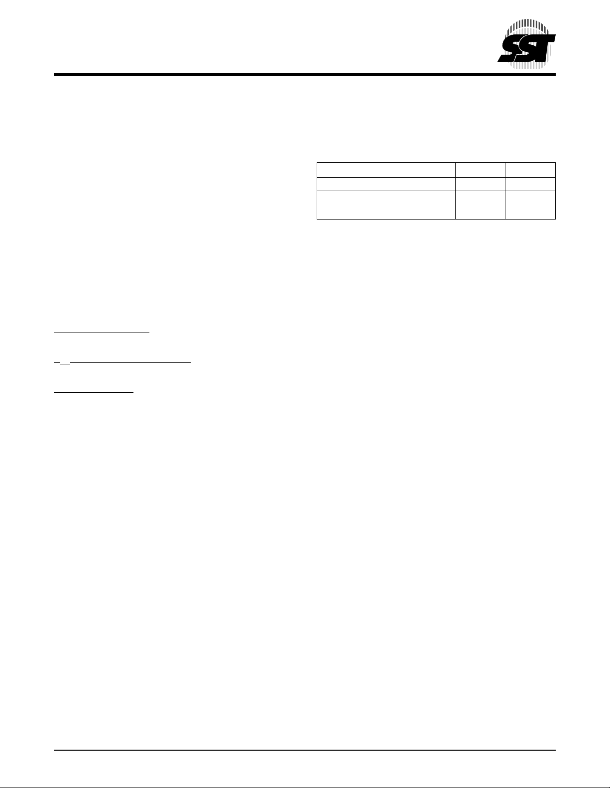
FUNCTIONAL BLOCK DIAGRAM
1 Mbit Multi-Purpose Flash
SST39LF100 / SST39VF100
Data Sheet
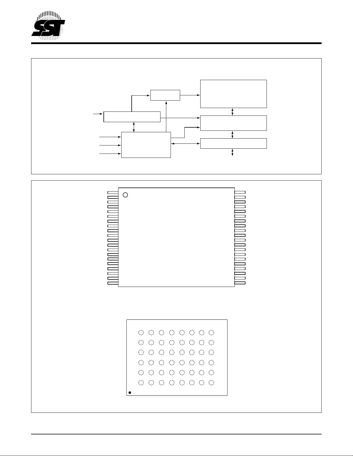
A0-A
15
CE#
OE#
WE#
Address Buffer & Latches
Control Logic
A10
A11
A12
A13
A14
A15
NC
WE#
V
DD
NC
CE#
DQ15
DQ14
DQ13
DQ12
DQ11
DQ10
DQ9
DQ8
A9
1
2
3
4
5
6
7
8
9
10
11
12
13
14
15
16
17
18
19
20
X-Decoder
I/O Buffers and Data Latches
Standard Pinout
T op Vie w
Die Up
SST39LF100/SST39VF100
SuperFlash
Memory
Y-Decoder
DQ15 - DQ
40
39
38
37
36
35
34
33
32
31
30
29
28
27
26
25
24
23
22
21
363 ILL F01.3
0
363 ILL B1.2
V
SS
A8
A7
A6
A5
A4
A3
A2
A1
A0
OE#
DQ0
DQ1
DQ2
DQ3
DQ4
DQ5
DQ6
DQ7
V
SS
TOP VIEW (balls facing down)
SST39LF/VF100
6
A13
A12
A14
A15
NC
NC
DQ15
V
SS
5
4
3
2
1
A9
WE#
NC
A7
A3
A8
NC
NC
NC
A4
A10
NC
NC
A6
A2
A11
NC
NC
A5
A1
DQ7
DQ5
DQ2
DQ0
A0
DQ14
DQ12
DQ10
DQ8
CE#
DQ13
V
DD
DQ11
DQ9
OE#
DQ6
DQ4
DQ3
DQ1
V
SS
363 ILL F02b.1
A B C D E F G H
FIGURE 1: PIN ASSIGN ME NTS FOR 40-LE A D TSOP AND 48-BALL TFBGA
©2001 Silicon Storage Technology, Inc. S71129-02-000 6/01 363
4

1 Mbit Multi-Purpose Flash
SST39LF100 / SST39VF100
Data Sheet
TABLE 2: PIN DESCRIPTION
Symbol Pin Name Functions
A
15-A0
-DQ
DQ
15
CE# Chip Enable To activate the device when CE# is low.
OE# Output Enable To gate the data output buffers.
WE# Write Enable To control the Write operations.
V
DD
V
SS
NC No Connection Unconnected pins.
TABLE 3: OPERATION MODES SELECTION
Mode CE# OE# WE# DQ Address
Read V
Program V
Erase V
Standby V
Write Inhibit X V
Product Identification
Software Mode V
1. X can be VIL or VIH, but no other value.
Address Inputs To provide memory addresses.
During Sector-Erase A
Data Input/output To output data during Read cycles and receive input data during Write cycles.
0
address lines will select the sector.
15-A11
Data is internally latched during a Write cycle.
The outputs are in tri-state when OE# or CE# is high.
Power Supply To provide power supply voltage: 3.0-3.6V for SST39LF100
2.7-3.6V for SST39VF100
Ground
V
IL
V
IL
V
IL
V
IL
IH
IH
IH
VILD
VILX
D
OUT
IN
1
A
IN
A
IN
Sector or Block address,
XXH for Chip-Erase
XXHigh Z X
IH
XHigh Z/ D
IL
XXVIHHigh Z/ D
V
IL
V
IL
IH
OUT
OUT
X
X
See Table 4
T2.2 363
T3.2 363
©2001 Silicon Storage Technology, Inc. S71129-02-000 6/01 363
5
1 Mbit Multi-Purpose Flash
SST39LF100 / SST39VF100
Data Sheet
TABLE 4: SOFTWARE COMMAND SEQUENCE
Command
Sequence
Word-Program 5555H AAH 2AAAH 55H 5555H A0H WA3Data
Sector-Erase 5555H AAH 2AAAH 55H 5555H 80H 5555H AAH 2AAAH 55H SA
Chip-Erase 5555H AAH 2AAAH 55H 5555H 80H 5555H AAH 2AAAH 55H 5555H 10H
Software ID Entry
Software ID Exit
Software ID Exit
1. Addres s format A14-A0 (Hex), Addres ses A15 can be VIL or VIH, but no other value, for the Command sequence
- DQ8 can be VIL or VIH, but no other value, for the Command sequence
2. DQ
15
3. WA = Program word address
for Sector-Erase; uses A15-A11 address lines
4. SA
X
5. The device does not remain in Software Product ID Mode if powered down.
6. With A
7. Both Software ID Exit operations are equivalent
5,6
7
7
=0; SST Manufacturer’s ID= 00BFH, is read with A0 = 0,
15-A1
1st Bus
Write Cycle
2nd Bus
Write Cycle
3rd Bus
Write Cycle
4th Bus
Write Cycle
5th Bus
Write Cycle
6th Bus
Write Cycle
Addr1Data2Addr1Data2Addr1Data2Addr1Data2Addr1Data2Addr1Data
4
X
5555H AAH 2AAAH 55H 5555H 90H
XXH F0H
5555H AAH 2AAAH 55H 5555H F0H
SST39LF100/SST39VF100 Device ID = 2788H, is read with A
0
= 1
30H
T4.4 363
2
Absolute Maximum Stress Ratings (Applied conditions greater than those listed under “Absolute Maximum
Stress Ratings” may cause pe r manent dama ge to the device. This is a stres s rating only and funct ional operatio n
of the device at these conditions or conditions greater tha n those defined in the ope rational sections of this data
sheet is not implied. Exposure to absolute maximum stress rating conditions may affect device reliability.)
Temperature Under Bias . . . . . . . . . . . . . . . . . . . . . . . . . . . . . . . . . . . . . . . . . . . . . . . . . . . . . . . . . -55°C to +125°C
Storage Temperature . . . . . . . . . . . . . . . . . . . . . . . . . . . . . . . . . . . . . . . . . . . . . . . . . . . . . . . . . . . -65°C to +150°C
D. C. Voltage on Any Pin to Ground Potential . . . . . . . . . . . . . . . . . . . . . . . . . . . . . . . . . . . . . . .-0.5V to V
Transient Voltage (<20 ns) on Any Pin to Ground Potential . . . . . . . . . . . . . . . . . . . . . . . . . . . .-1.0V to V
Voltage on A
Pin to Ground Potential . . . . . . . . . . . . . . . . . . . . . . . . . . . . . . . . . . . . . . . . . . . . . . . . -0.5V to 13.2V
9
+ 0.5V
DD
+ 1.0V
DD
Package Power Dissipation Capability (Ta = 25°C) . . . . . . . . . . . . . . . . . . . . . . . . . . . . . . . . . . . . . . . . . . . . . . 1.0W
Surface Mount Lead Soldering Temperature (3 Seconds) . . . . . . . . . . . . . . . . . . . . . . . . . . . . . . . . . . . . . . . 240°C
1
Output Short Circ uit Curr ent
1. Outputs shorted for no more than one second. No more than one output shorted at a time.
OPERATING RANGE: SST39LF100
Range Ambient Temp V
Commercial 0°C to +70°C 3.0-3.6V
. . . . . . . . . . . . . . . . . . . . . . . . . . . . . . . . . . . . . . . . . . . . . . . . . . . . . . . . . . . . . 50 mA
OPERATING RANGE: SST39VF100
DD
Range Ambient Temp V
DD
Commercial 0°C to +70°C 2.7-3.6V
Industrial -40°C to +85°C 2.7-3.6V
AC CONDITIONS OF TEST
Input Rise/Fall Time . . . . . . . . . . . . . . 5 ns
Output Load . . . . . . . . . . . . . . . . . . . . . C
Output Load . . . . . . . . . . . . . . . . . . . . . CL = 100 pF for SST39VF100
See Figures 11 and 12
= 30 pF for SST39LF100
L
©2001 Silicon Storage Technology, Inc. S71129-02-000 6/01 363
6

1 Mbit Multi-Purpose Flash
SST39LF100 / SST39VF100
Data Sheet
TABLE 5: DC OPERATING CHARACTERISTICS VDD = 3.0-3.6V FOR SST39LF100 AND 2.7-3.6V FOR SST39VF100
Limits
Symbol Parameter
I
DD
Power Supply Current Address input = VIL/VIH, at f=1/TRC Min.,
Read 30 mA CE#=OE#=V
Program and Erase 30 mA CE#=WE#=V
I
SB
I
LI
I
LO
V
IL
V
IH
V
IHC
V
OL
V
OH
Standby VDD Current 20 µA CE#=V
Input Leakage Current 1 µA VIN =GND to VDD, VDD = VDD Max.
Output Leakage Current 10 µA V
Input Low Voltage 0.8 VDD = VDD Min.
Input High Voltage 0.7V
Input High Voltage (CMOS) VDD-0.3 V VDD = VDD Max.
Output Low Voltage 0.2 V IOL = 5.8 mA, VDD = VDD Min.
Output Hi gh Voltage VDD-0.2 V IOH = -100 µA, VDD = VDD Min.
DD
Test ConditionsMin Max Units
V
DD=VDD
OUT
Max.
IL
IL
, VDD = VDD Max.
IHC
=GND to VDD, VDD = VDD Max.
VVDD = VDD Max.
,WE#=VIH, all I/Os open
, OE#=V
IH
T5.5 363
TABLE 6: RECOMMENDED SYSTEM POWER-UP TIMINGS
Symbol Parameter Minimum Units
T
T
1
PU-READ
PU-WRITE
1
1. This parameter is measured only for initial qualification and after a design or process change that could affect this parameter.
Power-up to Read Operation 100 µs
Power-up to Program/Erase Operation 100 µs
TABLE 7: CAPACITANCE (Ta = 25°C, f=1 Mhz, other pins open)
Parameter Description Test Condition Maximum
1
C
I/O
1
C
IN
1. This parameter is measured only for initial qualification and after a design or process change that could affect this parameter.
I/O Pin Capacitance V
= 0V 12 pF
I/O
Input Capacitance VIN = 0V 6 pF
TABLE 8: RELIABILITY CHARACTERISTICS
Symbol Parameter Minimum Specification Units Test Method
1
N
END
1
T
DR
1
I
LTH
1. This parameter is measured only for initial qualification and after a design or process change that could affect this parameter.
Endurance 10,000 Cycles JEDEC Standard A117
Data Retention 100 Years JEDEC Standard A103
Latch Up 100 + I
DD
mA JEDEC Standard 78
T6.0 363
T7.0 363
T8.1 363
©2001 Silicon Storage Technology, Inc. S71129-02-000 6/01 363
7
 Loading...