

Silicon Storage Technology Inc SST39VF512-70-4C-B3H, SST39VF512-55-4I-WK, SST39VF512-55-4I-WH, SST39VF512-55-4I-NK, SST39VF512-55-4I-NH Datasheet
...
512 Kbit / 1 Mbit / 2 Mbit / 4 Mbit (x8) Multi-Purpose Flash
SST39LF512 / SST39LF010 / SST39LF020 / SST39LF040
SST39VF512 / SST39VF010 / SST39VF020 / SST39VF040
SST39LF/VF512 / 010 / 020 / 0403.0 & 2.7V 512Kb / 1Mb / 2Mb / 4Mb (x8) MPF memories
FEATURES:
• Organized as 64K x8 / 128K x8 / 256K x8 / 512K x8
• Single V oltage Read and Write Operations
– 3.0-3.6V for SST39LF512/010/020/040
– 2.7-3.6V for SST39VF512/010/020/040
• Superior Reliability
– Endurance: 100,000 Cycles (typical)
– Greater than 100 years Data Retention
• Low Power Consumption:
– Ac ti ve Current: 10 mA (typical)
– Standby Current: 1 µA (typical)
• Sector-Erase Capability
– Uniform 4 KByte sectors
• Fast Read Access Time:
– 45 ns for SST39LF512/010/020/040
– 55 ns for SST39LF020/0 40
– 70 and 90 ns for SST39VF512/ 010/ 020 /040
• Latched Address and Data
• Fast Erase and Byte-Program:
– Sector-Erase Time: 18 ms (typical)
– Chip-Erase Time: 70 ms (typical)
– Byte-Program Time: 14 µs (typical)
– Chip Rewrite Time:
1 second (typical) for SST39LF/VF512
2 seconds (typical) for SST39LF/VF010
4 seconds (typical) for SST39LF/VF020
8 seconds (typical) for SST39LF/VF040
• Automatic Write Timing
– Internal V
Generation
PP
• End-of-Write Detection
– Toggle Bit
– Data# Polling
• CMOS I/O Compatibility
• JEDEC Standard
– Flash EEPROM Pinouts and command sets
• Packages Available
– 32-lead PLCC
– 32- l ead TSOP (8mm x 14mm)
– 48-ball TFBGA (6mm x 8mm) for 1 Mbit
Data Sheet
PRODUCT DESCRIPTION
The SST39LF512/010/020/040 and SST39VF512/010/
020/040 are 64K x8, 128K x8, 256K x8 and 5124K x8
CMOS Multi-Purpose Flash (MPF) manufactured with
SST’s proprietary, high performance CMOS SuperFlash
technology. The split-gate cell design and thick oxide tunneling injector atta in better reliability and manufacturability
compared with alternate approaches. The SST39LF512 /
010/020/040 devices wr ite (Program or Erase) with a 3.0-
3.6V power supply. The SST39VF512/010/020/040
devices write with a 2.7-3.6V power supply. The devices
conform to JEDEC standard pinouts for x8 memories.
Featuring high performance Byte-Program, the
SST39LF512/010/020/040 and SST39VF512/010/020/
040 devices provide a maxi mum Byte -Pr ogram time of 2 0
µsec. These devices use Toggle Bit or Data# Polling to indicate the completion of Program operation. To protect
against inadver ten t wri te, they have on-chip hardware an d
Software Data Protection schemes. Designed, manufactured, and tested for a wide spe ctr um of appl icatio ns, they
are offered with a guaranteed endurance of 10,000 cycles.
Data retention is rated at greater than 100 years.
The SST39LF512/010/020/040 and SST39VF512/010/
020/040 devices are suited for applications that require
convenient and economical updating of program, c onfiguration, or data memor y. For all system applica tions, they
significantly improves performance and reliability, while lowering power consumption. They inherently use less energy
during Erase and P rogram tha n alte r nat ive flash techn ologies. The total energy consumed is a function of the
applied voltage, cu rrent, an d time of appli cation. Si nce for
any given voltage range, the Supe rFlash te chnology uses
less current to program and has a shor ter era se time, the
total energy consumed during any Erase or Program operation is less than alternative flash technologies. These
devices also impr ove flexibility while lowering the c ost for
program, data, and configuration storage applications.
The SuperFlash te ch nology provides fixed Erase and P r ogram times, independent o f th e numbe r of Erase/ Pro gram
cycles that have occurred. Therefore the system software
or hardware does not have to be modified or de-rated as is
necessary with alternative flash technologies, whose Erase
and Program times i ncrease with accumul ated Erase/P rogram cycles .
To meet surface mount requirements, the SST39LF512/
010/020/040 and SST39VF512/010/020/040 devices are
offered in 32-lead PLCC and 32-lead TSOP packages. The
39LF/VF010 is also offered in a 48-ball TFBGA package.
See Figures 1 and 2 for pinouts.
©2001 Silicon Storage Technology, Inc.
S71150-03-000 6/01 395
1
The SST logo and SuperFlash are registered trademarks of Silicon Storage Technology, Inc.
MPF is a trademark of Silicon Storage Technology, Inc.
These specifications are subject to change without notice.

512 Kbit / 1 Mbit / 2 Mbit / 4 Mbit Multi-Purpose Flash
SST39LF512 / SST39LF010 / SST39LF020 / SST39LF040
SST39VF512 / SST39VF010 / SST39VF020 / SST39VF040
Data Sheet
Device Operation
Commands are used to initiate the memory operation functions of the device. Commands are written to the device
using standard microprocess or write sequences. A command is written by asse r ting WE# low whil e keeping CE#
low. The address bus is latched on the falling edge of WE#
or CE#, whichever occurs last. T he data bus is latc hed o n
the rising edge of WE# or CE#, whichever occurs first.
Read
The Read operation o f the S ST3 9LF 5 12/ 01 0/0 20/ 040 and
SST39VF512/010/020/040 device is controlled by CE#
and OE#, both have to be low for the system to obtain data
from the outputs. C E# is used for device selec tion. When
CE# is high, the chip is deselected and only standby power
is consumed. OE# is the output control and is used to gate
data from the outp ut pins. The data bus is in hi gh impedance state when e ither CE# or OE# is high. Refer to the
Read cycle timing diagra m f or further details (Figur e 4).
Byte-Program Operation
The SST39LF512/010/020/040 and SST39VF512/010/
020/040 are programmed on a byte-by-byte basis. Before
programming, one must ens ure that the sector, in which
the byte which is being programmed exists, is fully erased.
The Program operati on consists of three steps. Th e first
step is the three-byte-load sequence for Software Data
Protection. The second step is to load byte ad dress and
byte data. During the Byte-Program operation, the
addresses are latched on the falling edge of ei ther CE# or
WE#, whichever occurs last. The data is latched on the rising edge of either CE# or WE#, whichever occurs first. The
third step is the internal Program operat ion which is initiated after the rising edge of the fourth WE# or CE#, whichever occurs first. The Program operation, once initiated, will
be completed, within 20 µs. Se e Figures 5 and 6 for WE#
and CE# controlled Program operation timing diagrams
and Figure 15 for flowchar ts. During the Program ope ration, the only valid reads are Dat a# Polling and Toggle Bit.
During the inte rnal Program operat ion, the host is fre e to
perform additional tasks. Any commands written during the
internal Program operation will be ignored.
Sector-Erase Operation
The Sector-Erase operation allows the system to erase the
device on a sector-by-sector basis. The sector architecture
is based on unifor m sector size of 4 KByte. The S ectorErase operation is initiated by executing a six-byte-command sequence with Sector-Erase command (30H) and
sector address (SA) in the last bus cycle. The sector
address is latched on the falling edge of the sixth WE#
pulse, while the command (30H) is latched on the rising
edge of the sixth W E # pu ls e. The i nte rnal Erase op eratio n
begins after the sixth WE# pulse. The End-of-Erase can be
determined us ing either Data# Polling or Toggle Bit methods. See Figure 9 for timing waveforms. Any commands
written during the Sector-Erase operation will be ignored.
Chip-Erase Operation
The SST39LF512/010/020/040 and SST39VF512/010/
020/040 devices provide a Chip-Erase operation, which
allows the user to erase the entire memory array to the “1s”
state. This is useful when the entire device must be quickly
erased.
The Chip-Erase operation is initiated by executing a sixbyte Software Data Protection command sequence with
Chip-Erase command (10H) with address 5555H in the last
byte sequence. The inter nal Erase operation beg ins with
the rising edge of the sixt h WE # o r CE# , which ever oc cu rs
first. During the internal Erase operation, the only valid read
is T oggle Bit or Data# Polling. See Table 4 f or the command
sequence, Figure 10 for timing diagram, an d Figu re 18 for
the flowchart. Any commands written during the ChipErase operation will be ignored.
Write Operation Status Detection
The SST39LF512/010/020/040 and SST39VF512/010/
020/040 devices provide two software means to detect the
completion of a Write (Program or Erase) cycle, in order to
optimize the system write cycle time. The software detection includes two s ta tus b it s: Dat a# Polling (DQ
gle Bit (DQ
after the rising edge of WE# which initiates the internal Program or E rase op erat ion.
The actual comple tion of the n onvolatile write is as ync hronous with the sys tem; therefore, either a Data# Polling or
Toggle Bit read may be simultaneous wi th the complet ion
of the Write cycle. If this occurs, the system may possibly
get an erroneous result, i.e., valid data may appear to conflict with either DQ
rejection, if an erroneous result occurs, the software routine
should include a loop to read the accessed location an
additional two (2) times. If bo th reads are valid, then the
device has completed the Write cycle, otherwise the rejection is valid.
). The End-of-Write detection mode is enabled
6
or DQ6. In order to prevent spurious
7
) and Tog-
7
©2001 Silicon Storage Technology, Inc. S71150-03-000 6/01 395
2
512 Kbit / 1 Mbit / 2 Mbit / 4 Mbit Multi-Purpose Flash
SST39LF512 / SST39LF010 / SST39LF020 / SST39LF040
SST39VF512 / SST39VF010 / SST39VF020 / SST39VF040
Data Sheet
Data# Polling (DQ7)
When the SST39LF512/010/020/040 and SST39VF512/
010/020/040 are in the internal Program operation, any
attempt to read DQ
will produce the complement of the
7
true data. Onc e the P rogram ope ration is c ompl eted, D Q
will produce true data. The device is then ready for the next
operation. Duri ng inter nal E rase operation, any attempt t o
read DQ
tion is completed, DQ
will produce a ‘0’. Once the internal Erase opera-
7
will produce a ‘1’. The Data# Polling
7
is valid after the r ising edg e of four th WE# (or CE#) p ulse
for Program operation. For Sector- or Chip-Erase, the
Data# Polling is valid after the rising edg e of six th WE # ( or
CE#) pulse. See Figure 7 for Data# Polling timing dia gram
and Figure 16 for a flowchart.
Toggle Bit (DQ6)
During the inter nal Program or Erase ope ration, any consecutive attempts to read DQ
will produce alter nating 0s
6
and 1s, i.e., toggling between 0 and 1. W hen the internal
Program or Erase operation is com plete d, t he tog gling wi ll
stop. The device is then rea dy for the next operation. Th e
Toggle Bit is valid after the rising edge of fourth WE # (or
CE#) pulse for Program operation. For Sector- or ChipErase, the Toggle Bit is valid after the rising edge of sixth
WE# (or CE#) pulse. See Figure 8 for T oggle Bit timing diagram an d Figur e 16 f or a flo wcha rt.
Data Protection
The SST39LF512/010/020/040 and SST39VF512/010/
020/040 provide both hardware and software features to
protect non v ol atile d ata fr om inad ve rtent writes.
Hardware Data Protection
Noise/Glitch Protection: A WE# or CE# pulse of le ss than 5
ns will not init iate a Writ e cycle .
Power Up/Down Detection: The Write operation is
V
DD
inhibited when V
Write Inhibit Mode:
high will inhibit the W r ite operation. This prevents inadvertent writes during p ow er-up o r pow er- down.
is less than 1.5V.
DD
Forcing OE# low, CE# high, or WE#
Software Data Protection (SDP)
The SST39LF512/010/020/040 and SST39VF512/010/
020/040 provide the JEDEC approved Software Data Protection scheme for all data alteration operation, i.e., Program and Erase. Any Program operation requires the
7
inclusion of a series of three byte sequence. The three
byte-load sequence i s used to in itiate the P rogram operation, providing optimal protection from inadvertent Write
operations, e.g., during the system power-up or powerdown. Any Erase operation requires the inclusion of six
byte load sequence. These devices are shipped with th e
Software Data Protectio n pe rmanently ena bled. Se e Table
4 for the specific software co mmand codes. During SDP
command sequence, invalid commands will abort the
device to read mode, within T
RC
.
Product Identification
The Product Id entification mode ide ntifies the devices as
the SST39LF/VF512, SST39LF/VF010, SST39LF/VF020
and SST39LF/VF040 and manufacturer as SST. This
mode may be accessed by software operations. Users
may use the Software Pro duct Identification operation t o
identify the part (i.e., using the device ID) when using multiple manufacturers in the same socket. For details, see
Table 4 for software operation, Figure 11 for the Software
ID Entry and Read timing diagram, and F igure 17 for the
Software ID entry command sequence flowchart.
TABLE 1: P
Manufacturer’s ID 0000H BFH
Device ID
SST39LF/VF512 0001H D4H
SST39LF/VF010 0001H D5H
SST39LF/VF020 0001H D6H
SST39LF/VF040 0001H D7H
RODUCT IDENTIFICATION
Address Data
Product Identification Mode Exit/Reset
In order to return to the standard Read mode, the Software
Product Identific ation mode must be exited. Exit is acco mplished by issuing the Software ID Exit command
sequence, which returns the device to the Read operation.
Please note that the S oftware ID Exit command is ig nor e d
during an internal Program or Erase operation. See T able 4
for software command codes, Figure 12 for timing waveform, and Figure 17 for a flowchart.
T1.1 395
©2001 Silicon Storage Technology, Inc. S71150-03-000 6/01 395
3
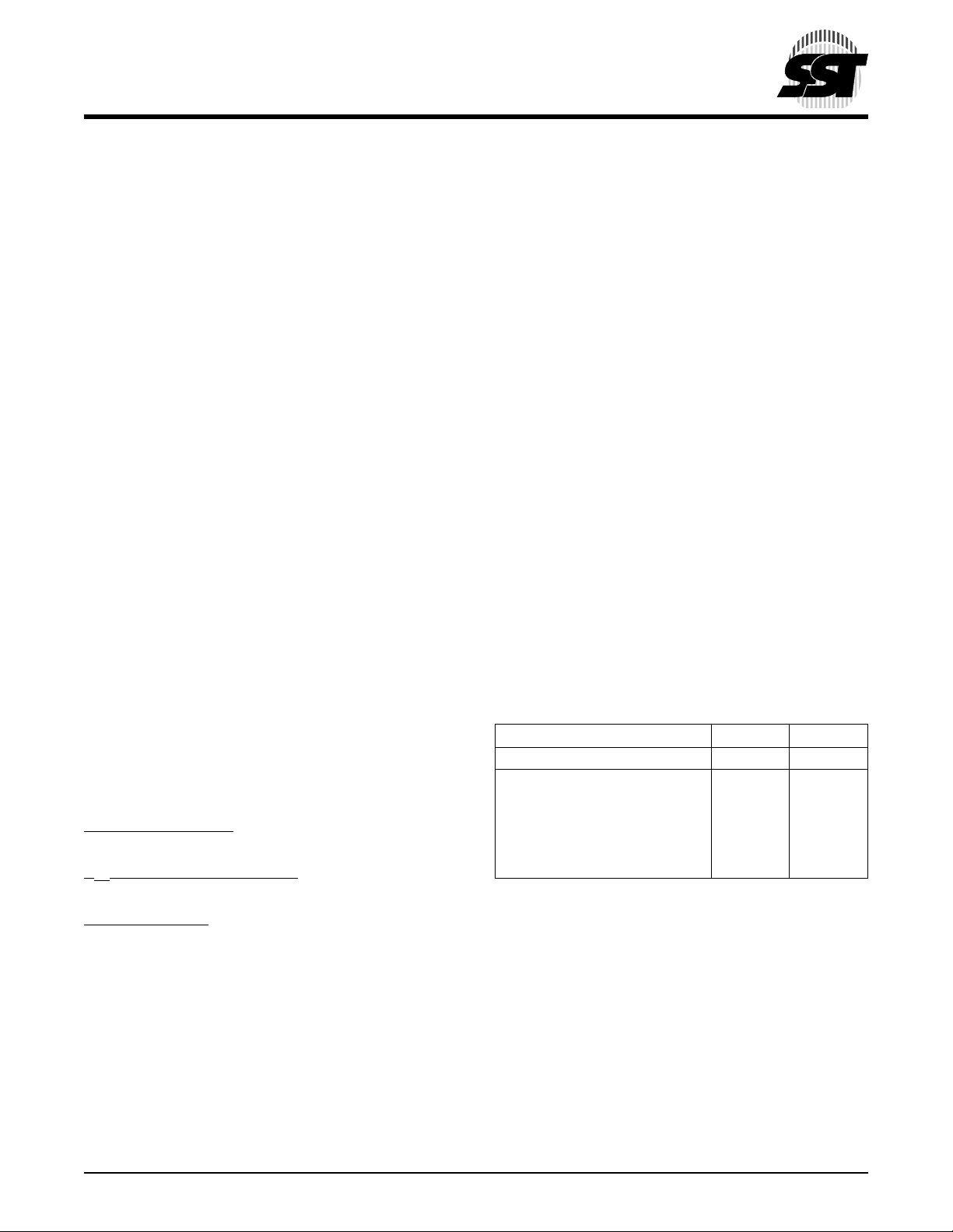
FUNCTIONAL BLOCK DIAGRAM
512 Kbit / 1 Mbit / 2 Mbit / 4 Mbit Multi-Purpose Flash
SST39LF512 / SST39LF010 / SST39LF020 / SST39LF040
SST39VF512 / SST39VF010 / SST39VF020 / SST39VF040
Data Sheet
Memory Address
Address Buffers & Latches
CE#
OE#
WE#
X-Decoder
Control Logic
A12
A12
A12
A15
A16
A18
A15
A16NCVDDWE#
A15
A16NCVDDWE#
VDDWE#
SuperFlash
Memory
Y-Decoder
I/O Buffers and Data Latches
DQ7 - DQ
A17
A17
NC
0
395 ILL B1.1
A7
A6
A5
A4
A3
A2
A1
A0
DQ0
A7
A6
A5
A4
A3
A2
A1
A0
DQ0
A7
A6
A5
A4
A3
A2
A1
A0
DQ0
A12
A15NCNC
SST39LF/VF512SST39LF/VF010SST39LF/VF020SST39LF/VF040 SST39LF/VF010 SST39LF/VF020 SST39LF/VF040SST39LF/VF512
A7
A6
A5
A4
A3
A2
A1
A0
DQ0
4 3 2 1 32 31 30
5
6
7
8
32-lead PLCC
9
10
11
12
13
SST39LF/VF512SST39LF/VF010SST39LF/VF020SST39LF/VF040 SST39LF/VF010 SST39LF/VF020 SST39LF/VF040SST39LF/VF512
T op Vie w
14 15 16 17 18 19 20
DQ1
DQ2
DQ1
DQ2
DQ1
DQ2
DQ1
DQ2
VDDWE#
NC
29
A14
28
A13
27
A8
26
A9
25
A11
24
OE#
23
A10
22
CE#
21
DQ7
SS
V
DQ3
DQ4
DQ5
DQ6
SS
V
DQ3
DQ4
DQ5
DQ6
SS
V
DQ3
DQ4
DQ5
DQ6
SS
V
DQ3
DQ4
DQ5
DQ6
395 ILL F02b.3
A14
A13
A8
A9
A11
OE#
A10
CE#
DQ7
A14
A13
A8
A9
A11
OE#
A10
CE#
DQ7
A14
A13
A8
A9
A11
OE#
A10
CE#
DQ7
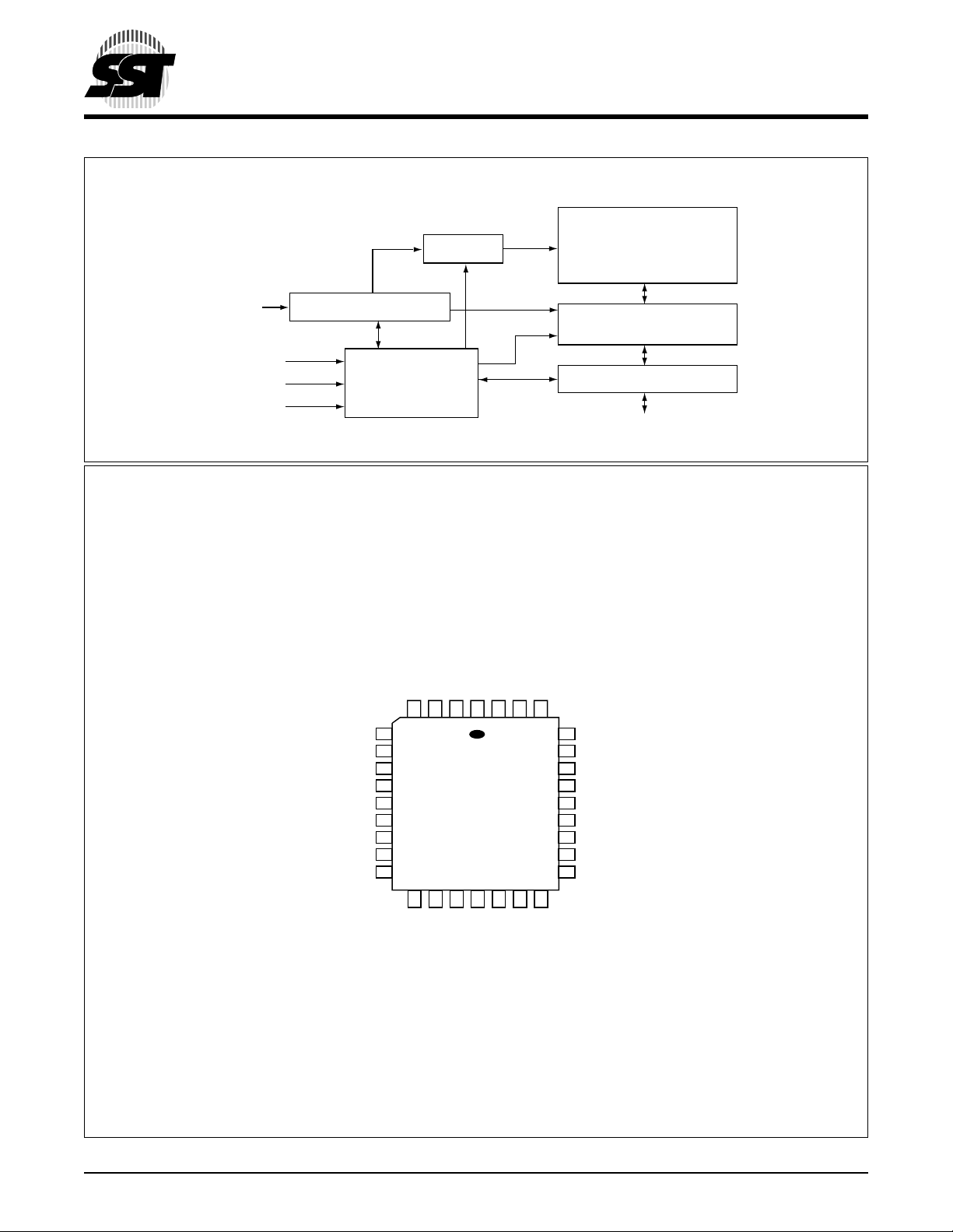
FIGURE 1: PIN ASSIGNMENTS FOR 32-LEAD PLCC
©2001 Silicon Storage Technology, Inc. S71150-03-000 6/01 395
4
512 Kbit / 1 Mbit / 2 Mbit / 4 Mbit Multi-Purpose Flash
SST39LF512 / SST39LF010 / SST39LF020 / SST39LF040
SST39VF512 / SST39VF010 / SST39VF020 / SST39VF040
Data Sheet
SST39LF/VF512SST39LF/VF010SST39LF/VF020SST39LF/VF040 SST39LF/VF010 SST39LF/VF020 SST39LF/VF040SST39LF/VF512
A11
A9
A8
A13
A14
A17
WE#
V
DD
A18
A16
A15
A12
A7
A6
A5
A4
FIGURE 2: PIN ASSIGNMENTS FOR 32-LEAD TSOP (8MM X 14MM)
A11
A13
A14
A17
WE#
V
DD
NC
A16
A15
A12
A9
A8
A7
A6
A5
A4
A11
A13
A14
WE#
V
A16
A15
A12
NC
DD
NC
A11
A9
A8
A7
A6
A5
A4
A13
A14
WE#
V
A15
A12
A9
A8
NC
DD
NC
NC
A7
A6
A5
A4
1
2
3
4
5
6
7
8
9
10
11
12
13
14
15
16
Standard Pinout
T op Vie w
Die Up
395 ILL F01.0
OE#
32
A10
31
CE#
30
DQ7
29
DQ6
28
DQ5
27
DQ4
26
DQ3
25
V
24
DQ2
23
DQ1
22
DQ0
21
A0
20
A1
19
A2
18
A3
17
OE#
A10
CE#
DQ7
DQ6
DQ5
DQ4
DQ3
V
DQ2
DQ1
DQ0
A0
A1
A2
A3
SS
SS
OE#
A10
CE#
DQ7
DQ6
DQ5
DQ4
DQ3
V
DQ2
DQ1
DQ0
A0
A1
A2
A3
SS
OE#
A10
CE#
DQ7
DQ6
DQ5
DQ4
DQ3
V
SS
DQ2
DQ1
DQ0
A0
A1
A2
A3
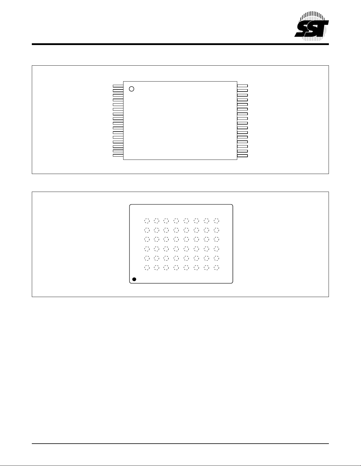
FIGURE 3: P
TOP VIEW (balls facing down)
SST39LF/VF010
6
A14
5
4
3
2
WE#
NC
1
A9
A7
A3
A13
A8
NC
NC
NC
A4
A15
A11
NC
NC
A6
A2
A16
A12
NC
NC
A5
A1
NC
NC
DQ5
DQ2
DQ0
A0
NC
A10
NC
DQ3
NC
CE#
NC
DQ6
V
DD
V
DD
NC
OE#
V
SS
DQ7
DQ4
NC
DQ1
V
SS
A B C D E F G H
IN ASSIGNMENT FOR 48-BALL TFBGA (6MM X 8MM) FOR 1 MBIT
395 ILL F01a.0.eps
©2001 Silicon Storage Technology, Inc. S71150-03-000 6/01 395
5
512 Kbit / 1 Mbit / 2 Mbit / 4 Mbit Multi-Purpose Flash
SST39LF512 / SST39LF010 / SST39LF020 / SST39LF040
SST39VF512 / SST39VF010 / SST39VF020 / SST39VF040
TABLE 2: PIN DESCRIPTION
Symbol Pin Name Functions
1
-A
A
MS
-DQ
DQ
7
CE# Chip Enable To activate the device when CE# is low.
OE# Output Enable To gate the data output buffers.
WE# Write Enable To control the Write operations.
V
DD
V
SS
NC No Connection Unconnected pins.
1. AMS = Most significant address
A
MS
Address Inputs To provide memory addresses. During Sector-Erase AMS-A12 address lines will s ele ct the
0
Data Input/output To output data during Read cycles and receive input data during Write cycles.
0
sector. During Block-Erase A
MS-A16
Data is internally latched during a Write cycle.
The outputs are in tri-state when OE# or CE# is high.
Power Supply To provide power supply voltage: 3.0-3.6V for SST39LF512/010/020/040
Ground
= A15 for SST39LF/VF512, A16 for SST39LF/VF010, A17 for SST39LF/VF020, and A18 for SST39LF/VF040
Data Sheet
address lines will select the block.
2.7-3.6V for SST39VF512/010/020/040
T2.1 395
TABLE 3: OPERATION MODES SELECTION
Mode CE# OE# WE# DQ Address
Read V
Program V
Erase V
Standby V
IL
IL
IL
IH
Write Inhibit X V
XXV
Product Identification
Software Mode V
1. X can be VIL or VIH, but no other value.
IL
V
IL
V
IH
V
IH
V
V
V
D
IH
IL
IL
D
X
OUT
IN
1
A
IN
A
IN
Sector address,
XXH for Chip-Erase
XXHigh Z X
IL
V
IL
XHigh Z/ D
High Z/ D
IH
V
IH
OUT
OUT
X
X
See Table 4
T3.4 395
©2001 Silicon Storage Technology, Inc. S71150-03-000 6/01 395
6
512 Kbit / 1 Mbit / 2 Mbit / 4 Mbit Multi-Purpose Flash
SST39LF512 / SST39LF010 / SST39LF020 / SST39LF040
SST39VF512 / SST39VF010 / SST39VF020 / SST39VF040
Data Sheet
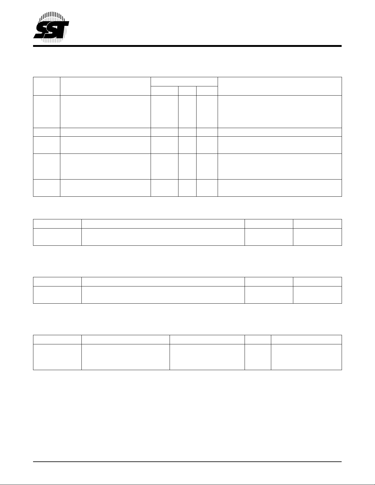
TABLE 4: SOFTWARE COMMAND SEQUENCE
Command
Sequence
Byte-Program 5555H AAH 2AAAH 55H 5555H A0H BA
Sector-Erase 5555H AAH 2AAAH 55H 5555H 80H 5555H AAH 2AAAH 55H SA
Chip-Erase 5555H AAH 2AAAH 55H 5555H 80H 5555H AAH 2AAAH 55H 5555H 10H
Software ID Entry
Software ID Exit
Software ID Exit
1. Address format A14-A0 (Hex),
2. BA = Program Byte address
for Sector-Erase; uses AMS-A12 address lines
3. SA
X
= Most significant address
A
MS
= A15 for SST39LF/VF512, A16 for SST39LF/VF010, A17 for SST39LF/VF020, and A18 for SST39LF/VF040
A
MS
4. The device does not remain in Software Product ID Mode if powered down.
5. With A
6. Both Software ID Exit operations are equivalent
4,5
6
6
Address A
Addresses A
Addresses A
Addresses A
=0; SST Manufacturer’s ID= BFH, is read with A0 = 0,
MS-A1
1st Bus
Write Cycle
2nd Bus
Write Cycle
3rd Bus
Write Cycle
4th Bus
Write Cycle
5th Bus
Write Cycle
6th Bus
Write Cycle
Addr1Data Addr1Data Addr1Data Addr1Data Addr1Data Addr1Data
2
Data
3
X
5555H AAH 2AAAH 55H 5555H 90H
XXH F0H
5555H AAH 2AAAH 55H 5555H F0H
can be VIL or VIH, but no other value, for the Command sequence for SST39LF/VF512.
15
can be VIL or VIH, but no other value, for the Command sequence for SST39LF/VF010.
15-A16
can be VIL or VIH, but no other value, for the Command sequence for SST39LF/VF020.
15-A17
can be VIL or VIH, but no other value, for the Command sequence for SST39LF/VF040.
15-A18
SST39LF/VF512 Device ID = D4H, is read with A
SST39LF/VF010 Device ID = D5H, is read with A
SST39LF/VF020 Device ID = D6H, is read with A
SST39LF/VF040 Device ID = D7H, is read with A
0
0
0
0
= 1
= 1
= 1
= 1
30H
T4.2 395
Absolute Maximum Stress Ratings (Applied conditions greater than those listed under “Absolute Maximum
Stress Ratings” may cause pe r manent dama ge to the device. This is a stres s rating only and funct ional operatio n
of the device at these conditions or conditions greater tha n those defined in the ope rational sections of this data
sheet is not implied. Exposure to absolute maximum stress rating conditions may affect device reliability.)
Temperature Under Bias . . . . . . . . . . . . . . . . . . . . . . . . . . . . . . . . . . . . . . . . . . . . . . . . . . . . . . . . . -55°C to +125°C
Storage Temperature . . . . . . . . . . . . . . . . . . . . . . . . . . . . . . . . . . . . . . . . . . . . . . . . . . . . . . . . . . . -65°C to +150°C
D. C. Voltage on Any Pin to Ground Potential . . . . . . . . . . . . . . . . . . . . . . . . . . . . . . . . . . . . . . .-0.5V to V
Transient Voltage (<20 ns) on Any Pin to Ground Potential . . . . . . . . . . . . . . . . . . . . . . . . . . . .-1.0V to V
Voltage on A
Pin to Ground Potential . . . . . . . . . . . . . . . . . . . . . . . . . . . . . . . . . . . . . . . . . . . . . . . . -0.5V to 13.2V
9
+ 0.5V
DD
+ 1.0V
DD
Package Power Dissipation Capability (Ta = 25°C) . . . . . . . . . . . . . . . . . . . . . . . . . . . . . . . . . . . . . . . . . . . . . . 1.0W
1
Output Short Circ uit Curr ent
1. Outputs shorted for no more than one second. No more than one output shorted at a time.
OPERATING RANGE FOR SST39L F512/010 /020/040
Range Ambient Temp V
Commercial 0°C to +70°C 3.0-3.6V
OPERATING RANGE FOR SST39V F51 2/010/020 /040
Range Ambient Temp V
Commercial 0°C to +70°C 2.7-3.6V
Industrial -40°C to +85°C 2.7-3.6V
. . . . . . . . . . . . . . . . . . . . . . . . . . . . . . . . . . . . . . . . . . . . . . . . . . . . . . . . . . . . . 50 mA
AC CONDITIONS OF TEST
DD
DD
Input Rise/Fall Time . . . . . . . . . . . . . . . 5 ns
Output Load
C
= 30 pF for SST39LF512/010/020/040
L
= 100 pF for SST39VF512/010/020/040
C
L
See Figures 13 and 14
©2001 Silicon Storage Technology, Inc. S71150-03-000 6/01 395
7
512 Kbit / 1 Mbit / 2 Mbit / 4 Mbit Multi-Purpose Flash
SST39LF512 / SST39LF010 / SST39LF020 / SST39LF040
SST39VF512 / SST39VF010 / SST39VF020 / SST39VF040
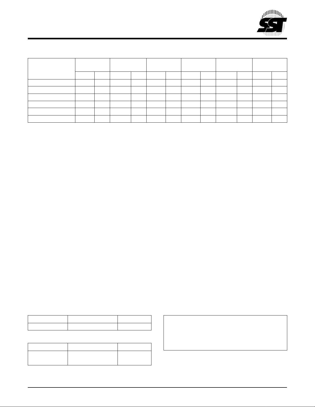
TABLE 5: DC OPERATING CHARACTERISTICS
VDD = 3.0-3.6V FOR SST39L F512/010/020/0 40 AND 2.7- 3.6V FOR SST39VF512/010/0 20/040
Symbol Parameter
I
DD
I
SB
I
LI
I
LO
V
IL
V
IH
V
IHC
V
OL
V
OH
Power Supply Current Address input=VIL/VIH, at f=1/TRC Min
Read 20 mA CE#=OE#=V
Write 20 mA CE#=WE#=V
Standby VDD Current 15 µA CE#=V
Input Leakage Current 1 µA VIN=GND to VDD, VDD=VDD Max
Output Leakage Current 10 µA V
Input Low Voltage 0.8 V VDD=VDD Min
Input High Voltage 0.7V
Input High Voltage (CMOS) VDD-0.3 V VDD=VDD Max
Output Low Voltage 0.2 V IOL=100 µA, VDD=VDD Min
Output Hi gh Voltage VDD-0.2 V IOH=-100 µA, VDD=VDD Min
DD
Limits
Test ConditionsMin Max Units
V
DD=VDD
OUT
Max
, VDD=VDD Max
IHC
=GND to VDD, VDD=VDD Max
VVDD=VDD Max
, WE#=VIH, all I/Os open
IL
, OE#=V
IL
IH
Data Sheet
T5.2 395
TABLE 6: RECOMMENDED SYSTEM POWER-UP TIMINGS
Symbol Parameter Minimum Units
T
T
1
PU-READ
PU-WRITE
1
1. This parameter is measured only for initial qualification and after a design or process change that could affect this parameter.
Power-up to Read Operation 100 µs
Power-up to Program/Erase Operation 100 µs
TABLE 7: CAPACITANCE (Ta = 25°C, f=1 Mhz, other pins open)
Parameter Description Test Condition Maximum
1
C
I/O
1
C
IN
1. This parameter is measured only for initial qualification and after a design or process change that could affect this parameter.
I/O Pin Capacitance V
= 0V 12 pF
I/O
Input Capacitance VIN = 0V 6 pF
TABLE 8: RELIABILITY CHARACTERISTICS
Symbol Parameter Minimum Specification Units Test Method
1
N
END
1
T
DR
1
I
LTH
1. This parameter is measured only for initial qualification and after a design or process change that could affect this parameter.
Endurance 10,000 Cycles JEDEC Standard A117
Data Retention 100 Years JEDEC Standard A103
Latch Up 100 + I
DD
mA JEDEC Standard 78
T6.1 395
T7.0 395
T8.2 395
©2001 Silicon Storage Technology, Inc. S71150-03-000 6/01 395
8
 Loading...