

Silicon Storage Technology Inc SST31LF043A-70-4E-WI, SST31LF043A-70-4E-WH, SST31LF043A-70-4C-WI, SST31LF043A-70-4C-WH, SST31LF043A-300-4E-WI Datasheet
...
4 Mbit Flash + 1 Mbit or 256 Kbit SRAM ComboMemory
SST31LF041 / SST31LF041A / SST31LF043 / SST31LF043A
SST31LF041 / 041A4Mb Flash (x8) + 1 Mb SRAM (x8) ComboMemories
FEATURES:
Data Sheet
• Monolithic Flash + SRAM ComboMemory
– SST31LF041/041A: 512K x8 Flash + 128K x8 SRAM
– SST31LF043/043A: 512K x8 Flash + 32K x8 SRAM
• Single 3.0-3.6V Read and Write Operations
• Concurrent Operation
– Read from or write to SRAM while
Erase/Program Flash
• Superior Reliability
– Endurance: 100,000 Cycles (typical)
– Greater than 100 years Data Retention
• Low Power Consumption:
– Active Current: 10 mA (typical) for Flash and
20 mA (typical) for SRAM Read
– Standby Current: 10 µA (typical)
• Flash Sector-Erase Capability
– Uniform 4 KByte sectors
• Latched Address and Data for Flash
PRODUCT DESCRIPTION
• Fast Read Access Times:
– SST31LF041/043 Flash: 70 ns
SRAM: 70 ns
– SST31LF041A/043A Flash: 300 ns
SRAM: 300 ns
• Flash Fast Erase and Byte-Program:
– Sector-Erase Time: 18 ms (typical)
– Bank-Erase Time: 70 ms (typical)
– Byte-Program Time: 14 µs (typical)
– Bank Rewrite Time: 8 seconds (typical)
• Flash Automatic Erase and Program Timing
– Internal V
Generation
PP
• Flash End-of-Write Detection
– Toggle Bit
– Data# Polling
• CMOS I/O Compatibility
• JEDEC Standard Command Set
• Packages Available
– 32-lead TSOP (8 x 14 mm) SST31LF041A/043A
– 40-lead TSOP (10 x 14 mm) SST31LF041/043
The SST31LF041/0 41A/043/043A devices are a 512K x8
CMOS flash memor y bank combined with a 128K x8 or
32K x8 CMOS SRAM memory bank manufactured with
SST’s proprieta ry, high performance SuperFl ash technol-
ogy. The SST31LF041/041A/043/043A devices write
(SRAM or flash) wi th a 3.0 -3 .6V power supply. The monolithic SST31LF041/041A/043/043A devices conform to
Software Data Protect (SDP) commands for x8
EEPROMs .
Featuring high performance Byte-Program, the flash memory bank provides a maxi mum Byte-Program time of 20
µsec. The entire f lash memory bank can be erase d and
programmed byte-by-byte in typically 8 seconds, when
using inter f ac e features such as Toggle Bit or Data # Polling
to indicate the completion of Program operation. To protect
against inadvertent flash write, the SST31LF041/041A/
043/043A devices have on-chip hardware and Software
Data Protection schemes. Designed, manufactured, and
tested for a wide spectrum of applications, the
SST31LF041/041A/043/043A devices are offered with a
guaranteed endurance of 10, 000 cycles. Data retent ion is
rated at greater than 100 years.
The SST31LF041/041A/043/043A operate as two independent memor y banks with re spective bank enable signals. The SRAM and Flash memory banks are
superimposed in the same memory address space. Both
memory ba nks share common address lines, data lines,
WE# and OE#. The memor y bank selection is done by
memory bank enable signals. The SRAM bank enable signal, BES# selects the SR AM bank and the flas h memor y
bank enable signal, B EF# s elects the f lash me mory bank.
The WE# signal has to be used with Software Data Protection (SDP) command sequence when controlling the Erase
and Program operatio ns in the flash memor y bank. The
SDP command seque nce protects the data stored in th e
flash memory bank from accidental alteration.
The SST31LF041/041A/043/043A provide the added functionality of being able to simulta neousl y read fro m or wr ite
to the SRAM bank while erasing or programming in the
flash memory ba nk. The SRAM m emory bank ca n be r ead
or written while the flash memory bank perfor ms SectorErase, Bank-Erase, or Byte-Program concurrently . All flash
memory Era se and Program operatio ns will automatic ally
latch the input ad dr ess a nd dat a s i gn als and c om pl ete th e
operation in background without further input stimulus
requirement. On ce the internall y controlled Erase or Program cycle in the fla sh bank has c ommenced , the SRAM
bank can be accessed for Read or Write.
The SST31LF041/041A/043/043A devices are suited for
applications that use both nonvolatile flash memory and
volatile SRAM memor y to stor e code or da ta. For all system applications, the SST31LF041/041A/043/043A
©2001 Silicon Storage Technology, Inc.
S71107-03-000 5/01 349
1
The SST logo and SuperFlash are registered trademarks of Silicon Storage Technology, Inc.
ComboMemory are trademarks of Silicon Storage Technology, Inc.
These specifications are subject to change without notice.

4 Mbit Flash + 1 Mbit or 256 Kbit SRAM ComboMemory
SST31LF041 / SST31LF041A / SST31LF043 / SST31LF043A
Data Sheet
devices significantly improve performance and reliability,
while lowering power consu mption, when compared with
multiple chip solu tions. The SST31LF041/041 A/043/043A
inherently use less energy during Erase and Program than
alternative flash te chnologies. Wh en programming a fla sh
device, the total energy consumed is a function of the
applied voltage, cu rrent, an d time of appli cation. Si nce for
any given voltage range, the Supe rFlash te chnology uses
less current to pr ogram and ha s a shor te r Erase t ime, the
total energy consumed during any Erase or Program operation is less than alternative flash technologies. The monolithic ComboMem or y elimi nates redu ndant fu nctions when
using two separate memories of similar architecture; therefore, reducing the total power consumption.
The SuperFlash te ch nology provides fixed Erase and P r ogram times, independent o f th e numbe r of Erase/ Pro gram
cycles that have occurred. Therefore the system software
or hardware does not have to be modified or de-rated as is
necessary with al ternativ e flas h techno logies , whos e Erase
and Program times i ncrease with accumul ated Erase/P rogram cycles .
The SST31LF041/041A/043/043A devices also improve
flexibility by using a single package and a common set of
signals to perfor m fun ct io ns previous ly req ui ring two separate devices. To meet high density, surface mount requirements, the SST31LF04 1/043 device is offered in 40-lead
TSOP package and the SST31LF041A/043A device is
offered in 32-lead TSOP package. See Figures 1 and 2 for
the pinouts.
Device Operation
The ComboMemory uses BES# and BEF# to control operation of either the SRA M or the flash memor y bank. Bus
contention is eliminated as the monolithi c device will not
recognize both bank enables as being simultaneously
active. If both bank enables are asser ted (i.e., BEF# and
BES# are both low), the BEF# will dominate while the
BES# is ignored and the appropriate operation will be executed in the flash memory bank. SST does not recommend
that both bank enables be simultaneously asserted. All
other address, data, and control lines are shared which
minimizes power consump tion and a rea. The device goes
into standby when both ba nk enables are raised to V
See T abl e 3 for SRAM operation mode selection.
For SST31LF041A/043A only: BES# and OE# share
pin 32. During SRAM operation, pin 32 will function as
BES#. During flash operation, pin 32 will function as OE#.
When pin 32 (OE#/BES#) is high, the data bus is in high
impedance state.
IHC
SRAM Operation
With BES# low and BEF# high, the SST31LF041/041A
operate as a 128K x8 CMOS SRAM and the
SST31LF043/043A operate as 32K x8 CMOS SRAM, with
fully static op eration requir ing no exter nal clocks or tim ing
strobes. The SRAM is mapped into the first 128 KByte
address space of the device for 041/041A or 32 KB yte for
043/043A. Read and Write cycle times are equal.
SRAM Read
The SRAM Read operation of the SST31LF041/041A/
043/043A are controlled by OE# and B ES #, bo th have to
be low with WE# high, for the system to obtain data from
the outputs. BES# is used for SRAM bank selection.
When BES# and BEF# are high, both memory banks are
deselected. OE# is the output control and is used to gate
data from the output pins. The data bus is in high impedance state when OE# is high. See Figure 3 for the Read
cycle timing diagram.
SRAM Write
The SRAM Write operation of the SST31LF041/041A/043/
043A is controlled by WE# and BES#; both have to be low
for the system to write to the SRAM. BES# is used for
SRAM bank selection. During the Byte-Write operation, the
addresses and da ta are referenced to the r ising edge of
either BES# or WE#, whichever occurs first. The Write time
is measured from the last falling edge to the first rising edge
of BES# and WE# . OE# can be V
value, for SRAM Write operations. See Figure 4 for the
SRAM Write cycle ti ming di agr am.
or VIH, but no other
IL
Flash Operation
With BEF# active, the SS T31LF 041/0 41A/ 043/04 3A o perate as a 51 2K x8 f la sh m em ory. The flash memo ry bank i s
read using the common address lines, data lines, WE# and
OE#. Erase and Program operations are initiated with the
JEDEC standard SDP command sequences. Address and
data are latched during the SDP commands and internally
timed Erase and Program operations. See T ab le 3 for flash
operation mode selection.
.
Flash Read
The Read operation of th e SST31LF041/041A/043/043A
devices are controlled by BE F# and O E #; b oth h ave to be
low, with WE# high, for the system to obtain data from th e
outputs. BEF# is used for flash memory bank selection.
When BEF# and BES# are high, both banks are deselected and only standby power is consumed. OE# i s the
©2001 Silicon Storage Technology, Inc. S71107-03-000 5/01 349
2

4 Mbit Flash + 1 Mbit or 256 Kbit SRAM ComboMemory
SST31LF041 / SST31LF041A / SST31LF043 / SST31LF043A
Data Sheet
output control and is used to gate data from the output pins.
The data bus is in high impedance state when OE# is high.
See Figure 5 for the Read cycle timing diagram.
Flash Erase/Program Operation
SDP command s are used to init iate the flash me mory bank
Program and Erase operation s of the S ST31LF0 41/041A /
043/043A. SDP comm ands are load ed to the flash me mory bank u sing stand ard mi crop roces sor wr i te se quences.
A command is loaded by asserting WE# low while keeping
BEF# low and OE# high. The address is latched on the falling edge of WE# or B EF#, whi che ver occu rs l ast. The d ata
is latched on the rising edge of WE# or BEF#, whichever
occurs first.
Flash Byte-Program Operation
The flash memory bank of the SST31LF041/041A/043/
043A devices are programmed on a byte-by-byte basis.
Before the Program operations, the memory must be
erased first. The Program operation consists of three steps.
The first step is the three-byte-load sequence for Software
Data Protection. The se cond step is to load byte address
and byte data. During the Byte-Program operation, the
addresses are latched on the falling edge of either BEF# or
WE#, whichever occurs last. The data is latched on the rising edge of either BEF# or WE#, whichever occurs first.
The third step is the internal Program operation which is initiated after the rising edge of the fourth WE# or BEF#,
whichever occurs first. The P rogram operation, once in itiated, will be completed, within 20 µs. See Figures 6 and 7
for WE# and BEF# controlled Program operation timing
diagrams and Figure 17 for flowcharts. During the Program
operation, the on ly valid Fl ash R ead o perati ons a re Data #
Polling and Toggle Bit. During the i nter nal Pr ogram operation, the host is free to pe rform additio nal tasks. Any SDP
commands load ed during the inter nal Program operation
will be ignored.
Flash Sector-Erase Operation
The Sector-Erase operation allows the system to erase the
flash memory bank on a sector-by-sector basis. The sector
architecture is based on uniform sector size of 4 KBy tes.
The Sector-Erase op eration is in itiated by executing a sixbyte-command load se quence for Software Data Protection with Sector-Erase command (30H) and sector address
(SA) in the last bus cy cle. The ad dress lines A
used to determ ine the sector addr es s. The s ector ad dr ess
is latched on the falling edge of the six th WE # pu ls e, whil e
the command (30H) is latched on the rising edge of the
sixth WE# pulse. The internal Erase operation begins after
the sixth WE# pul se . The End-o f-Er a se can be det ermined
18-A12
will be
using either Dat a# Polling or Toggle Bit methods. See Figure 10 for timing waveforms. Any SDP commands loaded
during the Sector-Erase operation will be ignored.
Flash Bank-Erase Operation
The SST31LF041/041A/043/043A flash memory bank provides a Bank-Erase operation, which allows the user to
erase the entire flash memory bank array to the “1s” state.
This is useful when the entire bank must be quickly erased.
The Bank-Erase operation is initiated by executing a sixbyte Software Data Protection command sequence with
Bank-Erase command (10H) with address 5555H in the last
byte sequence. The internal Erase operation begins with
the rising edge of the sixth WE# or BEF# pulse, whichever
occurs first. During the internal Erase operation, the only
valid Flash Read operations are Toggle Bit and Data# Polling. See Table 4 for the command sequence, Figure 11 for
timing diagram, and Figure 20 for the flowchart. Any SDP
commands loaded during the Bank-Erase operation will be
ignored.
Flash Write Operation Status Detection
The SST31LF041/041A/043/043A flash memory bank provides two software means to detect the completion of a
flash memory bank Write (Program or Erase) cycle, in
order to optimize the system Write cycle time. The software
detection includes two status bits: Data# Polling (DQ
Toggle Bit (DQ
). The End-of-Write detection mode is
6
) and
7
enabled after the rising edge of WE#, which initiate s the
internal Pr ogram or Erase operation. The a ctual completion of the nonvolatile write is a synchronous with th e system; therefore, either a Data# Polling or Toggle Bit Read
may be simultaneous with the completion of the Write
cycle. If thi s occurs, the system ma y possibl y get an errone ous result, i.e., valid data may appear to conflict with either
or DQ6. In order to prevent spurious reje ction, if an
DQ
7
erroneous result occurs, the software routine should
include a loop to read the acces sed lo cation an addit ional
two (2) times. If both read s are valid, then the device has
completed the Write cycl e, ot herwise t he rejection is v alid.
Flash Data# Polling (DQ7)
When the SST31LF041/041A/043/043A flash memory
bank is in th e internal P rogram operation, any atte mpt to
read DQ
Once the Program operation is completed, DQ
duce true d ata. The flash me mory bank is then ready for
the next operation. During internal Erase operation, any
attempt to read DQ
Erase operation is c omplete d, DQ
Data# Polling is valid after the rising edge of the fourth WE#
will produce the complement of the true data.
7
will pro-
7
will produce a ‘0’. Once the inter nal
7
will produce a ‘1’. The
7
©2001 Silicon Storage Technology, Inc. S71107-03-000 5/01 349
3

4 Mbit Flash + 1 Mbit or 256 Kbit SRAM ComboMemory
SST31LF041 / SST31LF041A / SST31LF043 / SST31LF043A
Data Sheet
(or BEF#) pulse for Program operation. For Sector or BankErase, t he Da ta# Pollin g i s valid afte r the risi ng edge o f t he
sixth WE# (or BEF#) pulse. See Figure 8 for Data# Polling
timing diagram and Figure 18 for a flowchart.
Flash Toggle Bit (DQ6)
During the inter nal Program or Erase ope ration, any consecutive attempts to read DQ
will produce alter nating 0s
6
and 1s, i.e., toggling between 0 and 1. W hen the internal
Program or Erase operation is com plete d, t he tog gling wi ll
stop. The flash memor y bank is then ready for the next
operation. The T oggle Bit is valid after the rising edge of the
fourth WE# (or BE#) pulse for Program operation. For Sector or Bank-Erase, the Toggle Bit is valid after the rising
edge of the sixth WE# (or BEF#) pulse. See Figur e 9 for
Toggle Bit timing diagram and Figure 18 for a flowchart.
Flash Memory Data Protection
The SST31LF041/041A/043/043A flash memory bank provides both hardware a nd sof tware features to pr otect no nvolatile data from inadvertent writes.
Flash Hardware Data Protection
Noise/Glitch Protection: A WE# or BEF# pulse of less than
5 ns will not initiate a Write cycle.
Power Up/Down Detection: The Write operation is
V
DD
inhibited when is less than 1.5V.
Write Inhibi t Mode: Forcing OE# low, BEF# high, or WE#
high will inhibit the Flash Write operation. This prevents
inadvertent writes during power-up or power-down.
Flash Software Data Protection (SDP)
The SST31LF041/041A/043/043A provide the JEDEC
approved Software Data Protection scheme for all flash
memory bank data alteration operations, i.e., Program and
Erase. Any Program operation req uires the inclusion of a
series of three-byte sequence. The three byte-load
sequence is used to initiate the Program operation, providing optimal protection from inadvertent Write operations,
e.g., during the system power-up or power-down. Any
Erase operation requires the inclusion of six-byte load
sequence. The SST3 1LF041/041A/043/0 43A devices are
shipped with the Software Data Protection permanently
enabled. See Table 4 for the specific software command
codes. During SDP command sequence, invalid SDP commands will abort the device to the Read mode, within T
RC
Concurrent Read and Write Operations
The SST31LF041/041A/043/043A provide the unique benefit of being able to read from or write to SRAM, while
simultaneously erasing or programming the Flash. The
device will ignore all SDP c ommands when an Erase or
Program operation is in progress. This allows dat a alteration code to be executed from SRAM, whil e altering the
data in Flash. The following table list s all valid state s. SST
does not recomme nd that both bank enables, BEF# an d
BES#, be simultaneously asserted.
ONCURRENT READ/WRITE STATE TABLE
C
Flash SRAM
Program/Erase Read
Program/Erase Write
Note that Product Identification commands use SDP;
therefore, these commands will also be ignored while an
Erase or Program operation is in progress.
Product Identification
The product id entification mode identifies the devices as
either SST31LF041/043 or SST31LF041A/043A and the
manufacturer as SST. This mode may be accessed by
hardware or software operations. The hardware device ID
Read operation is typ ica ll y us ed by a p r ogramm er to identify the correct algorithm for the SST31LF041/041A/043/
043A flash memory banks. Users may wish to use the software product identification operation to identify the part
(i.e., using the device ID) when usi ng multipl e manufacturers in the same socket. For details, see Table 3 for hardware ope r at io n or Table 4 for soft w a r e op eration, Fi gu re 12
for the software ID entry and read ti mi ng diagram and Figure 19 for the ID entry command sequence flowchart.
TABLE 1: PRODUCT IDENTIFICATION
Address Data
Manufacturer’s ID 0000H BFH
Device ID
SST31LF041 0001H 17H
SST31LF041A 0001H 16H
SST31LF043 0001H 65H
SST31LF043A 0001H 66H
T1.2 349
.
Product Identification Mode Exit/Reset
In order to return to the standard Read mode, the Software
Product Identification mode must be exited. Exiting is
accomplished by issuing the Exit ID command sequence,
©2001 Silicon Storage Technology, Inc. S71107-03-000 5/01 349
4
4 Mbit Flash + 1 Mbit or 256 Kbit SRAM ComboMemory
SST31LF041 / SST31LF041A / SST31LF043 / SST31LF043A
Data Sheet
which returns the device to the Read operation. Please
note that the software-reset command is ignored during an
internal Pr ogram or Erase op eration. See Table 4 for software command cod es, Figur e 13 for timin g waveform and
Figure 19 for a flowchart.
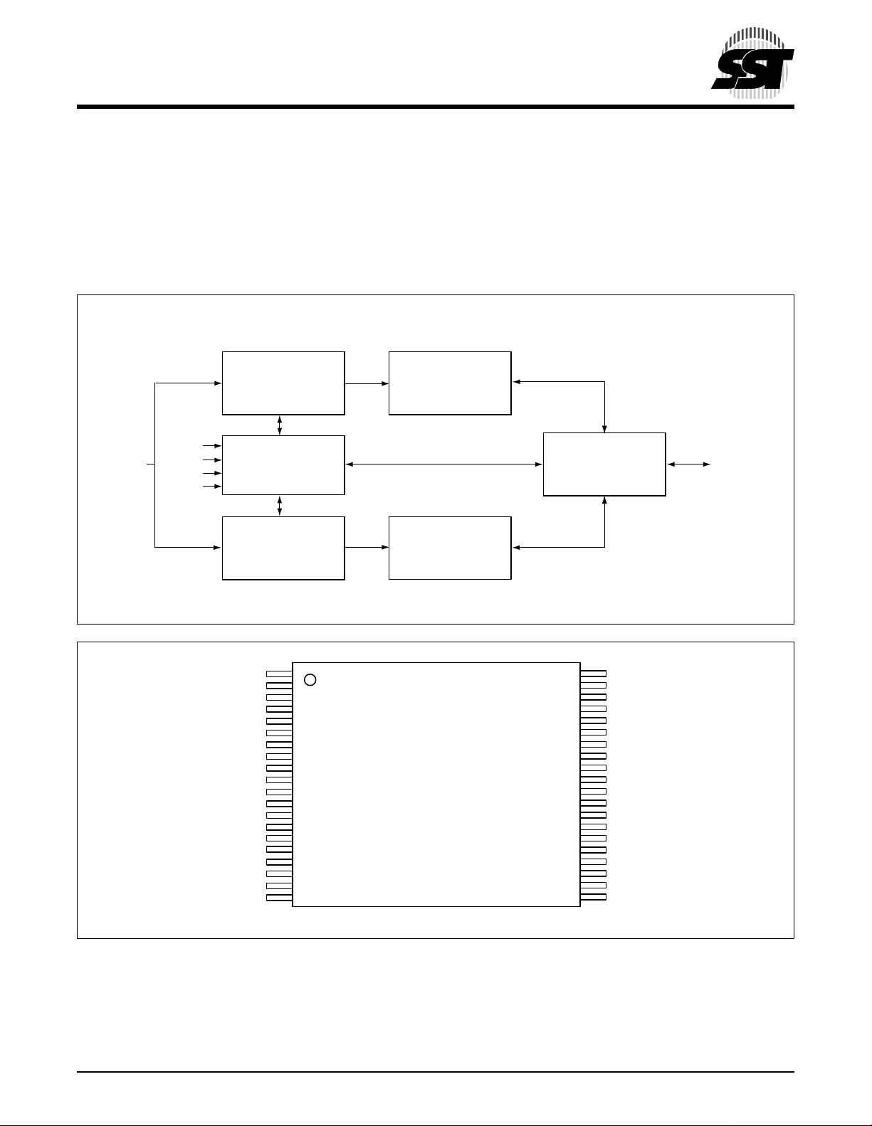
FUNCTIONAL BLOCK DIAGRAM
Address Buffers
BES#
AMS - A
BEF#
0
OE#
Control Logic
WE#
Address Buffers
& Latches
Design Considerations
SST recommends a high frequency 0.1 µF ceramic capacitor to be plac ed as close as possible between V
, e.g., less than 1 cm away from the VDD pin of the
V
SS
device. Additionally, a low frequency 4.7 µF electrolytic
capacitor from V
the V
SRAM
SuperFlash
Memory
DD
pin.
to VSS should be placed within 1 cm of
DD
I/O Buffers
DQ7 - DQ
DD
and
0
AMS = Most Significant Address
FIGURE 1: P
A16
A15
A14
A13
A12
A11
WE#
NC
BES#
NC
A18
1
2
3
4
5
A9
A8
A7
A6
A5
A4
A3
A2
A1
6
7
8
9
10
11
12
13
14
15
16
17
18
19
20
Standard Pinout
T op Vie w
Die Up
40
39
38
37
36
35
34
33
32
31
30
29
28
27
26
25
24
23
22
21
A17
V
NC
NC
A10
DQ7
DQ6
DQ5
DQ4
V
V
NC
DQ3
DQ2
DQ1
DQ0
OE#
V
BEF#
A0
349 ILL F01.2
SS
DD
DD
SS
IN ASSIGNMENTS FOR 40-LEAD TSOP (10MM X 14MM) - SSTLF041/043
349 ILL B1.6
©2001 Silicon Storage Technology, Inc. S71107-03-000 5/01 349
5
4 Mbit Flash + 1 Mbit or 256 Kbit SRAM ComboMemory
SST31LF041 / SST31LF041A / SST31LF043 / SST31LF043A
Data Sheet
A11
A13
A14
A17
WE#
V
DD
A18
A16
A15
A12
A9
A8
A7
A6
A5
A4
1
2
3
4
5
6
7
8
9
10
11
12
13
14
15
16
Standard Pinout
T op Vie w
Die Up
32
31
30
29
28
27
26
25
24
23
22
21
20
19
18
17
349 ILL F01A.1
OE#/BES#
A10
BEF#
DQ7
DQ6
DQ5
DQ4
DQ3
V
SS
DQ2
DQ1
DQ0
A0
A1
A2
A3
FIGURE 2: PIN ASSIGNMENTS FOR 32-LEA D TSOP (8MM X 14MM) - S STLF041 A/043A
TABLE 2: P
Symbol Pin Name Functions
1
-A
A
MS
-DQ0Data Input/output To output data during Read cycles and receive input data during Write cycles.
DQ
7
BES# SRAM Memory Bank Enable To activate the SRAM memory bank when BES# is low.
BEF# Flash Memory Bank Enable To activate the Flash memory bank when BEF# is low.
OE# Output Enable To gate the data output buffers.
WE# Write Enable To control the Write operations.
V
DD
V
SS
1. AMS = Most significant address
IN DESCRIPTION
Address Inputs To provide memory addresses. A18-A0 to provide flash address
0
to provide SRAM addresses for
A
16-A0
SST32LF041/041A
A14-A0 to provide SRAM addresses for
SST31LF043/043A
During flash Sector-Erase, A18-A12 address lines will select the sector.
Data is internal ly latched during a flash Erase/P rogram cycle.
The outputs are in tri-state when OE# or BES# and BEF# are high.
Note: For SST31LF041A/043A, BES# and OE# share pin 32.
Note: For SST31LF041A/043A, BES# and OE# share pin 32.
Power Supply 3.0-3.6V Power Supply
Ground
T2.11 349
©2001 Silicon Storage Technology, Inc. S71107-03-000 5/01 349
6
4 Mbit Flash + 1 Mbit or 256 Kbit SRAM ComboMemory
SST31LF041 / SST31LF041A / SST31LF043 / SST31LF043A
Data Sheet
TABLE 3: OPERATION MODES SELECTION
Mode BES#1BEF#1OE# WE# A9DQ Address
Flash
Read X
2
Program X V
Erase X V
SRAM
Read V
Write V
Standby V
IL
IL
IHC
Flash Write Inhibit X X V
XXXVIHXHigh Z / D
XVIHXXXHigh Z / D
Product Identification
Hardware Mode X V
Software Mode X V
1. BES# and BEF# cannot be asserted simultaneously. For SST31LF041A/043A BES# and OE# share pin 32.
When flash is active, pin 32 becomes OE#. When flash is inactive, pin 32 becomes BES#.
2. X can be V
3. Device ID 17H for SST31LF041, 16H for SST31LF041A, 65H for SST31LF043 and 66H for SST31LF043A.
or VIH, but no other value.
IL
V
IL
IL
IL
V
V
V
V
IL
IH
IH
AIND
IH
V
IL
V
IL
OUT
AIND
IN
X X Sector address,
A
IN
A
IN
XXH for Bank-Erase
V
IH
V
IH
V
IHC
IL
IL
V
XVILAIND
V
IL
AIND
IH
OUT
IN
A
IN
A
IN
XXXHigh Z X
IL
V
IL
V
IL
X X High Z / D
V
VHManufacturer’s ID (BFH)
IH
Device ID
V
AINID Code See Table 4
IH
OUT
OUT
OUT
3
X
X
X
A18-A1=VIL, A0=V
A18-A1=VIL, A0=V
IL
IH
T3.9 349
TABLE 4: SOFTWARE COMMAND SEQUENCE
Command
Sequence
Byte-Program 5555H AAH 2AAAH 55H 5555H A0H BA
Sector-Erase 5555H AAH 2AAAH 55H 5555H 80H 5555H AAH 2AAAH 55H SA
Bank-Erase 5555H AAH 2AAAH 55H 5555H 80H 5555H AAH 2AAAH 55H 5555H 10H
Software ID Entry
4,5
Software ID Exit 5555H AAH 2AAAH 55H 5555H F0H
1. Address format A14-A0 (Hex),Address A15-A18 can be VIL or VIH, but no other value, for the Command sequence.
2. BA = Program Byte address
3. SAX for Sector-Erase; uses A18-A12 address lines
4. The device does not remain in Software Product ID Mode if powered down.
5. With A
=0; SST Manufacturer’s ID= BFH, is read with A0 = 0,
18-A1
1st Bus
Write Cycle
1
Addr
Data Addr1Data Addr1Data Addr1Data Addr1Data Addr1Data
2nd Bus
Write Cycle
3rd Bus
Write Cycle
5555H AAH 2AAAH 55H 5555H 90H
SST31LF041 Device ID = 17H, is read with A
SST31LF041A Device ID = 16H, is read with A
SST31LF043 Device ID = 65H, is read with A
SST31LF043A Device ID = 66H, is read with A
= 1,
0
= 1
0
0
0
= 1
= 1
4th Bus
Write Cycle
2
Data
5th Bus
Write Cycle
6th Bus
Write Cycle
3
30H
X
T4.7 349
©2001 Silicon Storage Technology, Inc. S71107-03-000 5/01 349
7
4 Mbit Flash + 1 Mbit or 256 Kbit SRAM ComboMemory
SST31LF041 / SST31LF041A / SST31LF043 / SST31LF043A
Data Sheet
Absolute Maximum Stress Ratings (Applied conditions greater than those listed under “Absolute Maximum
Stress Ratings” may cause pe r manent dama ge to the device. This is a stres s rating only and funct ional operatio n
of the device at these conditions or conditions greater tha n those defined in the ope rational sections of this data
sheet is not implied. Exposure to absolute maximum stress rating conditions may affect device reliability.)
Operating Temperature . . . . . . . . . . . . . . . . . . . . . . . . . . . . . . . . . . . . . . . . . . . . . . . . . . . . . . . . . . . -20°C to +85°C
Storage Temperature . . . . . . . . . . . . . . . . . . . . . . . . . . . . . . . . . . . . . . . . . . . . . . . . . . . . . . . . . . . . -65°C to +150°C
D. C. Voltage on Any Pin to Ground Potential . . . . . . . . . . . . . . . . . . . . . . . . . . . . . . . . . . . . . . . .-0.5V to V
Transient Voltage (<20 ns) on Any Pin to Ground Potential. . . . . . . . . . . . . . . . . . . . . . . . . . . . . .-1.0V to V
Voltage on A
Pin to Ground Potential . . . . . . . . . . . . . . . . . . . . . . . . . . . . . . . . . . . . . . . . . . . . . . . . . -0.5V to 13.2V
9
Package Power Dissipation Capability (Ta = 25°C) . . . . . . . . . . . . . . . . . . . . . . . . . . . . . . . . . . . . . . . . . . . . . . 1.0W
Surface Mount Lead Soldering Temperature (3 Seconds). . . . . . . . . . . . . . . . . . . . . . . . . . . . . . . . . . . . . . . . 240°C
1
Output Short Circ uit Curr ent
1. Outputs shorted for no more than one second. No more than one output shorted at a time.
. . . . . . . . . . . . . . . . . . . . . . . . . . . . . . . . . . . . . . . . . . . . . . . . . . . . . . . . . . . . . . 50 mA
DD
DD
+0.5V
+1.0V
OPERATING RANGE
Range Ambient Temp V
Commercial 0°C to +70°C 3.0-3.6V
Extended -20°C to +85°C 3.0-3.6V
DD
AC CONDITIONS OF TEST
Input Rise/Fall Time . . . . . . . . . . . . . . . 5 ns
Output Load . . . . . . . . . . . . . . . . . . . . . C
See Figures 15 and 16
= 30 pF
L
©2001 Silicon Storage Technology, Inc. S71107-03-000 5/01 349
8
 Loading...