


SST29VE020-250-4I-WN
Silicon Storage Technology Inc SST29VE020-250-4I-WN, SST29VE020-250-4I-WH, SST29VE020-250-4I-UN, SST29VE020-250-4I-UH, SST29VE020-250-4I-PN Datasheet
...
©2001 Silicon Storage Technology, Inc.
S71062-06-000 6/01 307
1
The SST logo and SuperFlash are registered trademarks of Silicon Storage Technology, Inc.
SSF is a trademark of Silicon Storage Technology, Inc.
These specifications are subject to change without notice.
Data Sheet
2 Mbit (256K x8) Page-Mode EEPROM
SST29EE020 / SST29LE020 / SST29VE020
FEATURES:
• Single Voltage Read and Write Operations
– 5.0V-only for SST29EE020
– 3.0-3.6V for SST29LE020
– 2.7-3.6V for SST29VE020
• Superior Reliability
– Endurance: 100,000 Cycles (typical)
– Greater than 100 years Data Retention
• Low Power Consumption
– Active Current: 20 mA (typical) for 5V and
10 mA (typical) for 3.0/2.7V
– Standby Current: 10 µA (typical)
• Fast Page-Write Operation
– 128 Bytes per Page, 2048 Pages
– Page-Write Cycle: 5 ms (typical)
– Complete Memory Rewrite: 10 sec (typical)
– Effective Byte-Write Cycle Time: 39 µs (typical)
• Fast Read Access Time
– 5.0V-only operation: 120 and 150 ns
– 3.0-3.6V operation: 200 and 250 ns
– 2.7-3.6V operation: 200 and 250 ns
• Latched Address and Data
• Automatic Write Timing
– Internal V
PP
Generation
• End of Write Detection
– Toggle Bit
– Data# Polling
• Hardware and Software Data Protection
• Product Identification can be accessed via
Software Operation
• TTL I/O Compatibility
• JEDEC Standard
– Flash EEPROM Pinouts and command sets
• Packages Available
– 32-lead PLCC
– 32-lead TSOP (8mm x 14mm, 8mm x 20mm)
– 32-pin PDIP
PRODUCT DESCRIPTION
The SST29EE/LE/VE020 are 256K x8 CMOS Page-Write
EEPROM manufactured with SST’s proprietary, high per-
formance CMOS SuperFlash technology. The split-gate
cell design and th ick oxide tunneling injector attain better
reliability and manufacturability compared with alternate
approaches. The SST29EE/LE/VE020 write with a single
power supply. Internal Erase /Pro gram is transp ar en t to th e
user. The SST29EE/LE/VE020 conform to JEDEC stan-
dard pinouts for byte-wide memories.
Featuring high performance Page-Write, the SST29EE/LE/
VE020 provide a typica l Byte-Write time of 39 µsec. The
entire memor y, i.e., 256 KBytes, can be written page -by-
page in as litt le as 10 s econds, when u sing interface fea-
tures such as Toggle Bit or Data# Polling to indicate the
completion of a W ri te cy cle. To protect agains t inadvertent
write, the SST29EE/LE/VE020 have on-chip hardware and
Software Data Protection schemes. Designed, manufac-
tured, and tested for a wid e spectrum of ap plications, the
SST29EE/LE/VE02 0 are offered with a guaranteed Page-
Write endurance of 10,000 cycles. Data retention is rated at
greater th an 10 0 years .
The SST29EE/LE /VE020 are suited for applications that
require convenient and economi cal updating of program,
configuration, or data memory. For all system applicatio ns,
the SST29EE/ LE/VE020 signifi cantly imp rov e perf ormance
and reliability, while lowering power consumption. The
SST29EE/LE/VE 020 improve flexibility while lowering the
cost for program, data, and confi guration storage appli ca-
tions.
To meet high density, surface mount requirements, the
SST29EE/LE/VE020 are offered in 32-lead PLCC and 32-
lead TSOP packages. A 600-mi l, 32-pin P DIP package is
also available. See Figures 1, 2, and 3 for pinouts.
Device Operation
The SST Page-Mode EE PROM offers in-circuit electr ical
write capability. The SST29EE/LE/VE020 does not require
separate Erase and Program operations. The internally
timed Write c ycl e executes both erase and p ro gram t rans-
parently to the user. The SST29EE/LE/VE020 have indus-
try standard optional Software Data Protection, which SST
recommends always to be enabled. The SST29EE/LE/
VE020 are compatible with industry standard EEPROM
pinouts and functionality .
SST29EE020 / SST29LE020 / SST29VE0202 Mb Page-Mode flash memories

2
Data Sheet
2 Mbit Page-Mode EEPROM
SST29EE020 / SST29LE020 / SST29VE020
©2001 Silicon Storage Technology, Inc. S71062-06-000 6/01 307
Read
The Read operations o f th e SS T 29E E /LE /VE0 20 are con-
trolled by CE# and OE#, both have to be low for the system
to obtain data from the outputs. CE# is used for device
selection. When CE# is high, the chip is deselected and
only standby power is consumed. OE# is the output control
and is used to gate data from the output pins. The data bus
is in high impedance state when either CE# or OE# is high.
Refer to the Read cycle timing diagram for fur ther details
(Figure 4).
Write
The Page-Write to the SST29EE/LE/VE020 should always
use the JEDEC Stan dard So ftware Dat a P rotec ti on (SDP )
three-byte command s equen ce. The SST29 EE/L E/VE 020
contain the opti onal JED EC approved Software Dat a Pro-
tection scheme. SST recommends that SDP always be
enabled, thus, the description of the write operations will be
given using the SDP en abled format. The three-byte S DP
Enable and SDP Wr i te c o mma nd s a r e id en tic a l; therefore,
any time a SDP Write command is issued , Software Dat a
Protection is automatically assured. The first time the three-
byte SDP command is given, the device becomes SDP
enabled. Subsequent issuance of the same command
bypasses the data protection for the page being written. At
the end of the desired Page-Write, the entire device
remains protec ted. For addi tional de scr iptions, pl ease se e
the applicatio n not es The P r ope r Us e of JE DE C Sta nda r d
Software Data Protection and Protecting Against Uninten-
tional Writes When Using Single Power Supply Flash
Memories.
The Write ope ration consists o f three steps. Ste p 1 is the
three-byte load sequence for Software Data Protection.
Step 2 is the byte-load cycle to a page buffer of the
SST29EE/LE/VE020. Steps 1 and 2 use the same timing
for both operations. Step 3 is an internally controlled Write
cycle for writing the data loaded i n t he pag e buffer into th e
memory array for nonvolatile storage. During both the SDP
three-byte load sequence and the byte-load cycle, the
addresses are lat ched by the falling e dge of e ither CE# or
WE#, whichever occ ur s la st . Th e da ta is latched by the ris-
ing edge of either CE# or WE#, whichever occurs first. The
internal Write cycle is initiated by the T
BLCO
timer after the
rising edge o f WE# or CE#, whichever occurs first. The
Write cycle, once initiated, will continue to completion, typi-
cally within 5 ms. See Figur es 5 and 6 for WE# and CE#
controlled Page-Wr ite cycle timing diagrams and F igures
15 and 17 for flowcharts.
The Write op eration has three functional cycles : the Soft-
ware Data Protection loa d sequ ence, the page l oad c ycle,
and the internal Write cycle. The Software Data Protection
consists of a s pec ifi c t hr ee - byte lo ad sequence that allows
writing to the selected page an d will leave the SST29EE/
LE/VE020 protected at the end of the Page-Write. The
page load cycle consists of loading 1 to 128 Bytes of data
into the page buffer. The internal Write cycle consists of the
T
BLCO
time-out and the write timer operation. Dur ing the
Write operation, the only valid reads are Data# Polling and
Toggle Bit.
The Page-Write operation allow s the loading of up to 128
bytes of data into the page buffer of the SST29EE/LE/
VE020 before the initiation of the internal Write cycle. Dur-
ing the internal Write cycle, all the data in the page buffer is
written simultane ously into the me mory array. Hence, the
Page-Write feature of SST29EE/LE/VE020 allow the entire
memory to be written in as little as 10 seconds. During the
internal Wr ite cycle, the host is free t o perform additional
tasks, such as to fetch data from other locations in the sys-
tem to set up the write to the next page. In each Page-Write
operation, all the bytes that are loaded into the page buffer
must have the same page address, i.e. A
7
through A
16
. Any
byte not loaded with user data will be written to FFH.
See Figures 5 and 6 for the Page-Write cycle timing dia-
grams. If after the completio n of the three-byte SDP loa d
sequence or the initial byte-load cycle, the host loads a sec-
ond byte into the page buffer within a byte-load cycle time
(T
BLC
) of 100 µs, the SST29EE/LE/VE020 will stay in the
page load cycle. Additional bytes are then loaded consecu-
tively. The page load cycle will be terminated if no addi-
tional byte is loaded into the page buffer within 200 µs
(T
BLCO
) from the last byte-load c ycle, i.e., no subsequent
WE# or CE# hig h-to -lo w t ran siti on after the la st risi ng ed ge
of WE# or CE#. Data in the page buffer can be changed by
a subsequent byte-load cyc le. The page load period can
continue indefin itely, as long as the host co ntinues to load
the device within the byte-load cycle time of 100 µs. The
page to be loaded is d etermined by the page address of
the last byte loaded.
Software Chip-Erase
The SST29EE/LE/VE020 provide a Chip-Erase operation,
which allows the user to simultaneously clear the entire
memory array to the “1” state. This is useful when the entire
device must be quickly erased.
The Software Chip- Erase operation is i nitiated by using a
specific six-byte l oad sequence. After th e load sequence,
the device enters into an internally timed cycle similar to the
Write cycle. During the Erase operation, the only valid read
is Toggle Bit. See T ab le 4 for the load sequence, Figure 10
for timing diagram, and Figure 19 for the flowchart.

Data Sheet
2 Mbit Page-Mode EEPROM
SST29EE020 / SST29LE020 / SST29VE020
3
©2001 Silicon Storage Technology, Inc. S71062-06-000 6/01 307
Write Operation Status Detection
The SST29EE/LE/VE020 provide two software means to
detect the completi on of a W r ite c yc le, in or d er to o pti mi ze
the system Write cycle time. The software detection
includes two status bits: Data# Polling (DQ
7
) and T oggle Bit
(DQ
6
). The end of write detection mode is enabled after the
rising WE# or CE# whichever occurs first, wh ich initiates
the internal Write cycle .
The actual completion of the nonvolatile write is asynchro-
nous with the system ; therefore, either a Data# Polling or
Toggle B it read may be simultaneous with the complet ion
of the Write cycle. If this occurs, the system may possibly
get an erroneous result, i.e., valid data may appear to con-
flict with either DQ
7
or DQ
6
. In order to prevent spurious
rejection, if an erroneous result occurs, the software routine
should include a loop to read the accessed location an
additional two (2) times. If bo th reads are valid, then the
device has completed the Write cycle, otherwise the rejec-
tion is valid.
Data# Polling (DQ
7
)
When the SST29EE/LE/VE020 are in the internal Write
cycle, any attempt to read DQ
7
of the last byte loaded dur-
ing the byte-load cycle wil l receive the complem ent of the
true data. Once the Write cycle is completed, DQ
7
will
show true data. The device is then ready for the next opera-
tion. See Figure 7 for Data# Polling timing diagram and Fig-
ure 16 for a flowchart.
Toggle Bit (DQ
6
)
During the internal Write cycle , any consecu tive attemp ts to
read DQ
6
will produce alter nating 0s and 1s, i.e., toggling
between 0 and 1. When the Wr ite c ycle is co mpleted , the
toggling will stop. The device is then ready for the next
operation. See Fig ure 8 for Toggle Bit timing diagram and
Figure 16 for a flowchart. The initial read of the Toggle Bit
will typically be a “1”.
Data Protection
The SST29EE/LE/ VE 02 0 pr ovid e b oth ha r dware an d so ft-
ware features to protect nonvolatile data from inadverten t
writes.
Hardware Data Protection
Noise/Glitch Protection: A WE# or CE# pulse of l ess th an 5
ns will not init iate a Writ e cycle .
V
DD
Power Up/Down Detection: The Write operation is
inhibited when V
DD
is less than 2.5V.
Write Inhibit Mode:
Forcing OE# low, CE# high, or WE#
high will inhibit the W r it e operation. This prevents inadvert-
ent writes during p ow er-u p or po wer- dow n.
Software Data Protection (SDP)
The SST29EE/LE/VE020 provide the JEDEC approved
optional Software Data Protection scheme for all data alter-
ation operations, i.e., Write and Chip-Erase. With this
scheme, any Write operation requires the inclusion of a
series of three byte-load operations to precede the data
loading operation. The three byte-load sequence is used to
initiate the Write cycle, providing optimal protection from
inadvertent write operations, e.g., during the system power-
up or power-down. The SST29 EE/LE/VE020 are shippe d
with the Software Data Protection disabled.
The software protection s cheme can be enabled by apply-
ing a three-byte sequenc e to the device, during a page-
load cycle (Figures 5 and 6). The device will then be auto-
matically set into the data protect mode. Any subsequent
Write operation will require the preceding three-byte
sequence. See Table 4 for the specific software comm an d
codes and Figures 5 and 6 for the timin g diagrams. To set
the device into the unprotected mode, a six-byte sequence
is required. See Table 4 for the specific codes and Figure 9
for the timing diagram. If a write is attempte d while SDP is
enabled the device will be in a non-accessible state for
~300 µs. SST recommends Software Data Protection
always be enabled. See Figure 17 for flowcharts.
The SST29EE/LE/VE020 Software Data Protection is a
global command, protecting all pages in the entire memory
array once enabled (or disabled). Therefore using SDP for
a single Page-Write will enable SDP for the entire array.
Single pages by themse lves cannot be SDP ena bl ed or
disabled.
Single power supply reprogrammable nonvolatile memo-
ries may be unintentionally altered. SST strongly recom-
mends that Software Data Protection (SDP) always be
enabled. The SST29EE/LE/VE020 should be programmed
using the SDP command sequence. SST recommends the
SDP Disable Command Seq uence not be issued to the
device prior to w riting.
Please refer to the following Application Notes for more
informati on on using SDP:
• Protecting Against Unintentional Writes When
Using Single Power Supply Flash Memories
• The Proper Use of JEDEC Standard Software
Data Protection
4
Data Sheet
2 Mbit Page-Mode EEPROM
SST29EE020 / SST29LE020 / SST29VE020
©2001 Silicon Storage Technology, Inc. S71062-06-000 6/01 307
Product Identification
The product id enti fic ati on mode ident ifi es the de vi ce as the
SST29EE/LE/VE020 and manufacturer as SST. This mode
is accessed via so ftware. For details, see Table 4, Figur e
11 for the software ID entr y and r ead timing diagram, an d
Figure 18 for the ID entry command sequence flowchart.
Product Identification Mode Exit
In order to retur n to the sta nda rd r ead mod e, the So ftware
Product Identification mode must be exited. Exiting is
accomplished b y issuing the Softw are ID Exit (reset) oper a-
tion, which ret urns the device to the Re ad operation. Th e
Reset operation may also be used to reset the device to the
Read mode after an inadvertent transient condition that
apparently causes the device to behave abnorma lly, e.g.,
not read correctly. See Table 4 for software command
codes, Figure 12 for timing waveform, and Figu re 18 for a
flowchart.
FIGURE 1: P
IN ASSIGNMENTS FOR 32-LEAD PLCC
TABLE 1: P
RODUCT IDENTIFICATION
Address Data
Manufacturer’s ID 0000H BFH
Device ID
SST29EE020 0001H 10H
SST29LE020 0001H 12H
SST29VE020 0001H 12H
T1.3 307
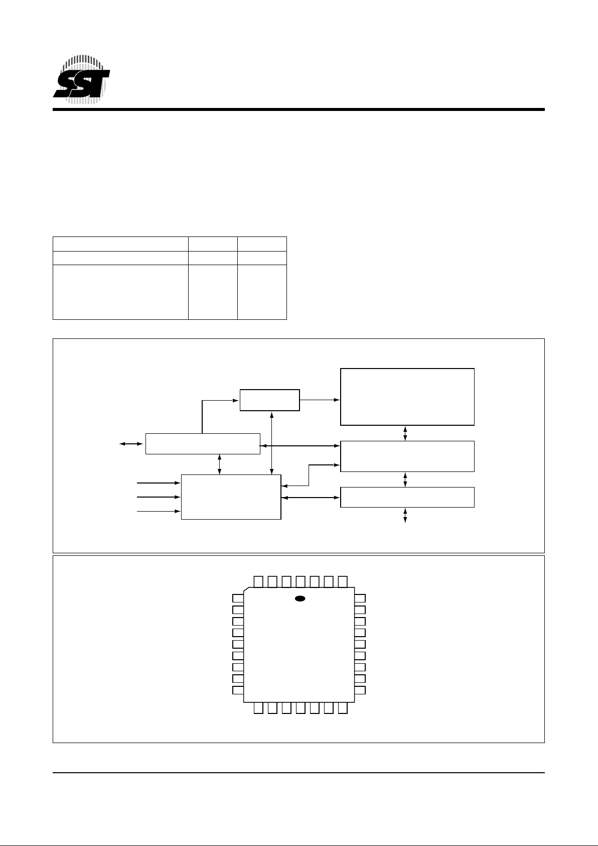
Y-Decoder and Page Latches
I/O Buffers and Data Latches
307 ILL B1.1
Address Buffer & Latches
X-Decoder
DQ
7
- DQ
0
A
17
- A
0
WE#
OE#
CE#
SuperFlash
Memory
Control Logic
FUNCTIONAL BLOCK DIAGRAM
5
6
7
8
9
10
11
12
13
29
28
27
26
25
24
23
22
21
A7
A6
A5
A4
A3
A2
A1
A0
DQ0
A14
A13
A8
A9
A11
OE#
A10
CE#
DQ7
4 3 2 1 32 31 30
A12
A15
A16
NC
V
DD
WE#
A17
32-lead PLCC
T op Vie w
307 ILL F02.3
14 15 16 17 18 19 20
DQ1
DQ2
V
SS
DQ3
DQ4
DQ5
DQ6
Data Sheet
2 Mbit Page-Mode EEPROM
SST29EE020 / SST29LE020 / SST29VE020
5
©2001 Silicon Storage Technology, Inc. S71062-06-000 6/01 307
FIGURE 2: PIN ASSIGNMENTS FOR 32-LEAD TSOP
FIGURE 3: P
IN ASSIGNMENTS FOR 32-PIN PDIP
A11
A9
A8
A13
A14
A17
WE#
V
DD
NC
A16
A15
A12
A7
A6
A5
A4
1
2
3
4
5
6
7
8
9
10
11
12
13
14
15
16
OE#
A10
CE#
DQ7
DQ6
DQ5
DQ4
DQ3
V
SS
DQ2
DQ1
DQ0
A0
A1
A2
A3
32
31
30
29
28
27
26
25
24
23
22
21
20
19
18
17
307 ILL F01.2
Standard Pinout
T op Vie w
Die Up
1
2
3
4
5
6
7
8
9
10
11
12
13
14
15
16
32-pin
PDIP
T op Vie w
307 ILL F19.0
NC
A16
A15
A12
A7
A6
A5
A4
A3
A2
A1
A0
DQ0
DQ1
DQ2
V
SS
32
31
30
29
28
27
26
25
24
23
22
21
20
19
18
17
V
DD
WE#
A17
A14
A13
A8
A9
A11
OE#
A10
CE#
DQ7
DQ6
DQ5
DQ4
DQ3
TABLE 2: PIN DESCRIPTION
Symbol Pin Name Functions
A
17
-A
7
Row Address Inputs To provide memory addresses. Row addresses define a page for a Write cycle.
A
6
-A
0
Column Address Inputs Column Addresses are toggled to load page data
DQ
7
-DQ
0
Data Input/output To output data du ring Read cycles and receive input data during Wri te cycles.
Data is internally latched during a Write cycle.
The outputs are in tri-state when OE# or CE# is high.
CE# Chip Enable To activate the device when CE# is low.
OE# Output Enable To gate the data output buffers.
WE# Write Enable To control the Write operations.
V
DD
Power Supply To provide: 5.0V supply (±10%) for SST29EE020
3.0V supply (3.0-3.6V) for SST29LE020
2.7V supply (2.7-3.6V) for SST29VE020
V
SS
Ground
NC No Connection Unconnected pins.
T2.2 307

6
Data Sheet
2 Mbit Page-Mode EEPROM
SST29EE020 / SST29LE020 / SST29VE020
©2001 Silicon Storage Technology, Inc. S71062-06-000 6/01 307
TABLE 3: OPERATION MODES SELECTION
Mode CE# OE# WE# DQ Address
Read V
IL
V
IL
V
IH
D
OUT
A
IN
Page-Write V
IL
V
IH
V
IL
D
IN
A
IN
Standby V
IH
X
1
XHigh Z X
Write Inhibit X V
IL
XHigh Z/ D
OUT
X
XXV
IH
High Z/ D
OUT
X
Software Chip-Erase V
IL
V
IH
V
IL
D
IN
A
IN,
See Table 4
Product Identification
Software Mode V
IL
V
IH
V
IL
Manufacturer’s ID (BFH)
Device ID
2
See Table 4
SDP Enable Mode V
IL
V
IH
V
IL
See Table 4
SDP Disable Mode V
IL
V
IH
V
IL
See Table 4
T3.3 307
1. X can be V
IL
or V
IH
, but no other value
2. Device ID = 10H for SST29EE020 and 12H for SST29LE/VE020
TABLE 4: SOFTWARE COMMAND SEQUENCE
Command
Sequence
1st Bus
Write Cycle
2nd Bus
Write Cycle
3rd Bus
Write Cycle
4th Bus
Write Cycle
5th Bus
Write Cycle
6th Bus
Write Cycle
Addr
1
1. Address format A
14
-A
0
(Hex), Addres s A
15
can be V
IL
or V
IH
, but no other value.
Data Addr
1
Data Addr
1
Data Addr
1
Data Addr
1
Data Addr
1
Data
Software
Data Protect Enable
& Page-Write
5555H AAH 2AAAH 55H 5555H A0H Addr
2
2. Page-Write consists of loading up to 128 Bytes (A
6
-A
0
)
Data
Software
Data Protect Disable
5555H AAH 2AAAH 55H 5555H 80H 5555H AAH 2AAAH 55H 5555H 20H
Software Chip-Erase
3
3. The software Chip-Erase function is not supported by the industrial temperature part.
Please contact SST if you require this function for an industrial temperature part.
5555H AAH 2AAAH 55H 5555H 80H 5555H AAH 2AAAH 55H 5555H 10H
Software ID Entry
4,5
4. The device does not remain in Software Product ID Mode if powered down.
5. With A
14
-A
1
=0; SST Manufacturer’s ID= BFH, is read with A
0
= 0,
SST29EE020 Device ID = 10H, is read with A
0
= 1
SST29LE/VE020 Device ID = 12H, is read with A
0
= 1
5555H AAH 2AAAH 55H 5555H 90H
Software ID Exit 5555H AAH 2AAAH 55H 5555H F0H
Alternate
Software ID Entry
6
6. Alternate six-byte Software Product ID Command Code
Note: This product supports both the JEDEC standard three-byte command code sequence and SST’s original six-byte command code
sequence. For new designs, SST recommends that the three-byte command code sequence be used.
5555H AAH 2AAAH 55H 5555H 80H 5555H AAH 2AAAH 55H 5555H 60H
T4.2 307
Data Sheet
2 Mbit Page-Mode EEPROM
SST29EE020 / SST29LE020 / SST29VE020
7
©2001 Silicon Storage Technology, Inc. S71062-06-000 6/01 307
Absolute Maximum Stress Ratings (Applied conditions greater than those listed under “Absolute Maximum
Stress Ratings” may cause pe r manent dama ge to the device. This is a stres s rating only and funct ional operatio n
of the device at these conditions or conditions greater tha n those defined in the ope rational sections of this data
sheet is not implied. Exposure to absolute maximum stress rating conditions may affect device reliability.)
Temperature Under Bias . . . . . . . . . . . . . . . . . . . . . . . . . . . . . . . . . . . . . . . . . . . . . . . . . . . . . . . . . -55°C to +125°C
Storage Temperature . . . . . . . . . . . . . . . . . . . . . . . . . . . . . . . . . . . . . . . . . . . . . . . . . . . . . . . . . . . -65°C to +150°C
D. C. Voltage on Any Pin to Ground Potential . . . . . . . . . . . . . . . . . . . . . . . . . . . . . . . . . . . . . . .-0.5V to V
DD
+ 0.5V
Transient Voltage (<20 ns) on Any Pin to Ground Potential . . . . . . . . . . . . . . . . . . . . . . . . . . . .-1.0V to V
DD
+ 1.0V
Voltage on A
9
Pin to Ground Potential . . . . . . . . . . . . . . . . . . . . . . . . . . . . . . . . . . . . . . . . . . . . . . . . -0.5V to 14.0V
Package Power Dissipation Capability (Ta = 25°C) . . . . . . . . . . . . . . . . . . . . . . . . . . . . . . . . . . . . . . . . . . . . . . 1.0W
Through Hold Lead Soldering Temperature (10 Seconds) . . . . . . . . . . . . . . . . . . . . . . . . . . . . . . . . . . . . . . . 300°C
Surface Mount Lead Soldering Temperature (3 Seconds) . . . . . . . . . . . . . . . . . . . . . . . . . . . . . . . . . . . . . . . 240°C
Output Short Circ uit Curr ent
1
. . . . . . . . . . . . . . . . . . . . . . . . . . . . . . . . . . . . . . . . . . . . . . . . . . . . . . . . . . . . 100 mA
1. Outputs shorted for no more than one second. No more than one output shorted at a time.
OPERATING RANGE FOR SST29E E020
Range Ambient Temp V
DD
Commercial 0°C to +70°C5.0V±10%
Industrial -40°C to +85°C5.0V±10%
OPERATING RANGE FOR SST29L E02 0
Range Ambient Temp V
DD
Commercial 0°C to +70°C 3.0-3.6V
Industrial -40°C to +85°C 3.0-3.6V
OPERATING RANGE FOR SST29V E020
Range Ambient Temp V
DD
Commercial 0°C to +70°C 2.7-3.6V
Industrial -40°C to +85°C 2.7-3.6V
AC CONDITIONS OF TEST
Input Rise/Fall Time . . . . . . . . . . . . . . 10 ns
Output Load . . . . . . . . . . . . . . . . . . . . . 1 TTL Gate and C
L
= 100 pF
See Figures 13 and 14
8
Data Sheet
2 Mbit Page-Mode EEPROM
SST29EE020 / SST29LE020 / SST29VE020
©2001 Silicon Storage Technology, Inc. S71062-06-000 6/01 307
TABLE 5: DC OPERATING CHARACTERISTICS V
DD
= 5.0V±10% FOR SST 29E E020
Symbol Parameter
Limits
Test ConditionsMin Max Units
I
DD
Power Supply Current Address input=V
IL
/V
IH
, at f=1/T
RC
Min,
V
DD
=V
DD
Max
Read 30 mA CE#=OE#=V
IL
, WE#=V
IH
, all I/Os open
Write 50 mA CE#=WE#=V
IL
, OE#=V
IH
, V
DD
=V
DD
Max
I
SB1
Standby V
DD
Current
(TTL input)
3 mA CE#=OE#=WE#=V
IH
, V
DD
=V
DD
Max
I
SB2
Standby V
DD
Current
(CMOS input)
50 µA CE#=OE#=WE#=V
DD
-0.3V, V
DD
=V
DD
Max
I
LI
Input Leakage Current 1 µA V
IN
=GND to V
DD
, V
DD
=V
DD
Max
I
LO
Output Leakage Current 10 µA V
OUT
=GND to V
DD
, V
DD
=V
DD
Max
V
IL
Input Low Voltage 0.8 V V
DD
=V
DD
Min
V
IH
Input High Voltage 2 .0 V V
DD
=V
DD
Max
V
OL
Output Low Voltage 0.4 V I
OL
=2.1 mA, V
DD
=V
DD
Min
V
OH
Output High Voltage 2.4 V I
OH
=-400 µA, V
DD
=V
DD
Min
T5.2 307
TABLE 6: DC OPERATING CHARACTERISTICS V
DD
= 3.0-3.6V FOR SST29LE020 AND 2.7-3.0V FOR SST29VE020
Symbol Parameter
Limits
Test ConditionsMin Max Units
I
DD
Power Supply Current Address input=V
IL
/V
IH
, at f=1/T
RC
Min,
V
DD
=V
DD
Max
Read 12 mA CE#=OE#=V
IL
, WE#=V
IH
, all I/Os open
Write 15 mA CE#=WE#=V
IL
, OE#=V
IH
, V
DD
=V
DD
Max
I
SB1
Standby V
DD
Current
(TTL input)
1 mA CE#=OE#=WE#=V
IH
, V
DD
=V
DD
Max
I
SB2
Standby V
DD
Current
(CMOS input)
15 µA CE#=OE#=WE#=V
DD
-0.3V, V
DD
=V
DD
Max
I
LI
Input Leakage Current 1 µA V
IN
=GND to V
DD
, V
DD
=V
DD
Max
I
LO
Output Leakage Current 10 µA V
OUT
=GND to V
DD
, V
DD
=V
DD
Max
V
IL
Input Low Voltage 0.8 V V
DD
=V
DD
Min
V
IH
Input High Voltage 2 .0 V V
DD
=V
DD
Max
V
OL
Output Low Voltage 0.4 V I
OL
=100 µA, V
DD
=V
DD
Min
V
OH
Output High Voltage 2.4 V I
OH
=-100 µA, V
DD
=V
DD
Min
T6.2 307
 Loading...