

Page 1
INSTRUCTION: Z-Wave 700 Integration Guide
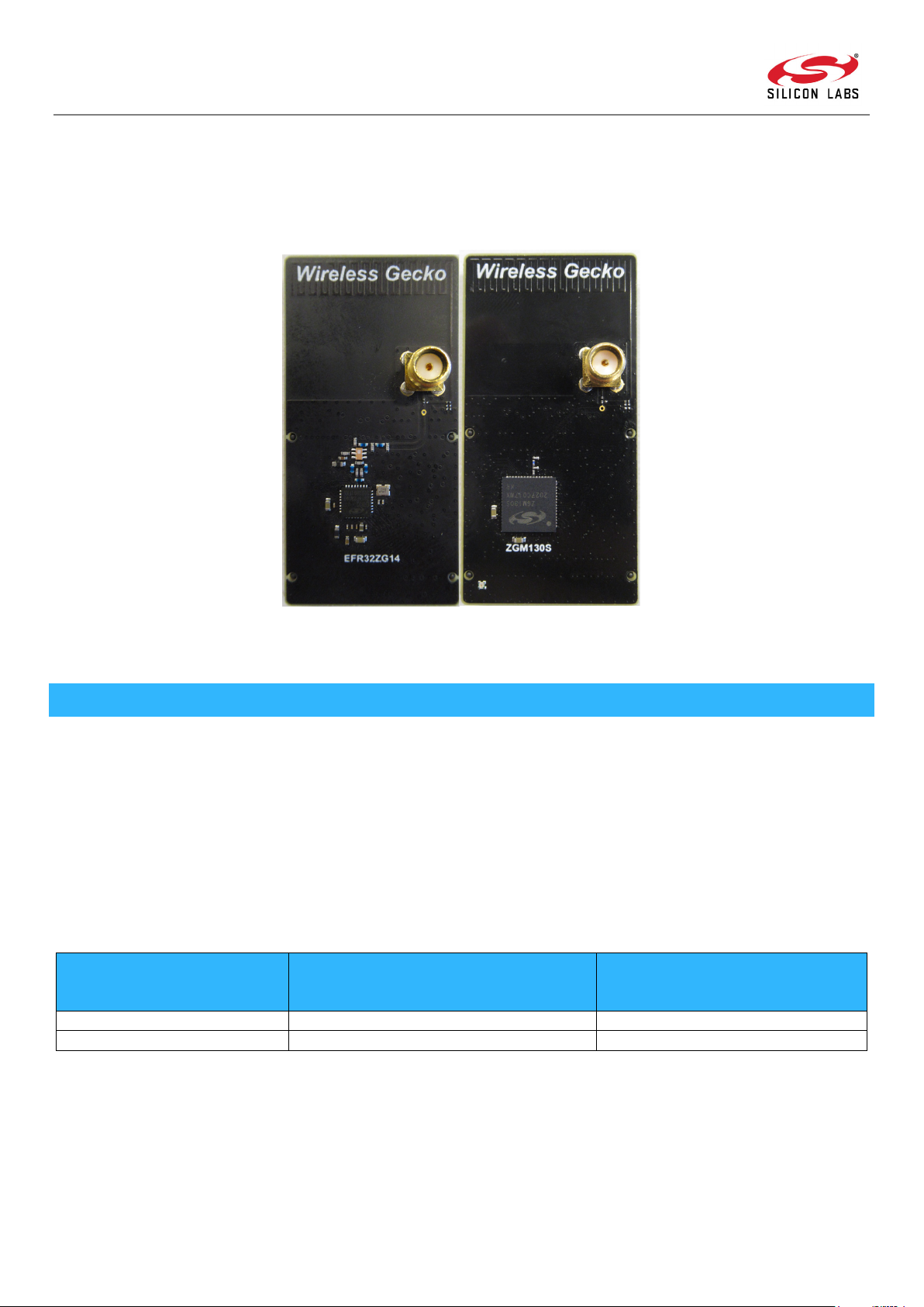
QFN32
5mm x 5mm
LGA64
9mm x 9mm
Chip
EFR32ZG14
Module
ZGM130S
INTEGRATION GUIDE FOR SILICON LABS ZENGECKO Z-WAVE® DEVICES
The purpose of this document is to provide an implementation guide for integrating Z-Wave 700 devices into product designs.
It is intended for product design engineers who aim for a fast integration of Z-Wave 700 devices.
1 OVERVIEW
The Z-Wave 700 device portfolio is shown in Table 1.1. The EFR32ZG14 SoC exposes the Z-Wave serial API via UART and is dedicated
to gateway applications. The ZGM130S SiP module combines a general-purpose SoC, crystal, supply decoupling components, and
RF matching components into a single small-footprint module requiring only two decoupling capacitors. The ZGM130S is mainly
targeted at end device applications and, with its built-in ARM M4 core and ultra-low power consumption, it is perfect for making
single chip sensors and other end devices that require advanced processing and low power consumption. Alternatively, the
ZGM130S SiP module can be used in gateway applications as well.
Please refer to [1] for an overview of supported Z-Wave regions and frequency bands supported by the Z-Wave protocol.
Table 1.1: Z-Wave 700 device portfolio
Type
SoC
SiP
The applicable modules are clearly stated at the beginning of each of the following sections.
INS14487-6 | 3/2021 1
Page 2

Instruction: Z-Wave Z-Wave 700 Integration Guide
2 CONTENT
1 OVERVIEW ........................................................................................................................................................................ 1
3 PROGRAMMING AND DEBUGGING INTERFACE .................................................................................................................. 3
3.1 PROGRAMMING INTERFACE OVERVIEW ......................................................................................................................................... 4
4 CALIBRATION .................................................................................................................................................................... 4
4.1 CRYSTAL ................................................................................................................................................................................. 4
5 RF VERIFICATION TOOL ...................................................................................................................................................... 4
6 COMPONENT SPECIFICATIONS ........................................................................................................................................... 5
6.1 SAW FILTER ........................................................................................................................................................................... 5
6.1.1 Recommended Components for GSM/LTE gateways .................................................................................................. 7
6.1.2 OPTIONAL Components for GSM/LTE gateways ......................................................................................................... 7
6.1.3 Z-Wave protocol support for optional SAW filter bank ............................................................................................... 7
6.2 CRYSTAL ................................................................................................................................................................................. 7
6.2.1 Recommended Components ....................................................................................................................................... 8
7 SUPPLY FILTER ................................................................................................................................................................... 8
8 MATCHING CIRCUIT ........................................................................................................................................................... 9
8.1 SUMMARY OF MATCHING + FILTERING NETWORKS .......................................................................................................................... 9
8.2 SOC TO RF LINE MATCHING ..................................................................................................................................................... 10
8.2.1 Mandatory Components for General Z-Wave ........................................................................................................... 12
8.2.2 Mandatory Components for Z-Wave Long Range ..................................................................................................... 12
8.3 ADDITIONAL FILTERING FOR Z-WAVE LONG RANGE ........................................................................................................................ 12
8.4 RF LINE TO ANTENNA MATCHING ............................................................................................................................................... 13
8.5 MEASUREMENT SETUP ............................................................................................................................................................ 14
9 PCB IMPLEMENTATION ................................................................................................................................................... 14
9.1 PLACEMENT .......................................................................................................................................................................... 14
9.2 STACK-UP ............................................................................................................................................................................. 15
9.3 POWER ROUTING ................................................................................................................................................................... 15
9.4 DECOUPLING ......................................................................................................................................................................... 15
9.4.1 For ZGM130S SiP MODULE ........................................................................................................................................ 15
9.4.2 For EFR32ZG14 SoC ................................................................................................................................................... 16
9.5 RF TRACE ............................................................................................................................................................................. 16
9.6 IC GROUNDING ..................................................................................................................................................................... 17
10 ANTENNA DESIGN........................................................................................................................................................ 17
11 ESD .............................................................................................................................................................................. 18
12 ABBREVIATIONS .......................................................................................................................................................... 19
13 REVISION HISTORY ...................................................................................................................................................... 22
14 REFERENCES ................................................................................................................................................................ 23
2 INS14487-6 | 3/2021
Page 3
Instruction: Z-Wave 700 Integration Guide
EFR32ZG14
ZGM130S
Applicable
Applicable
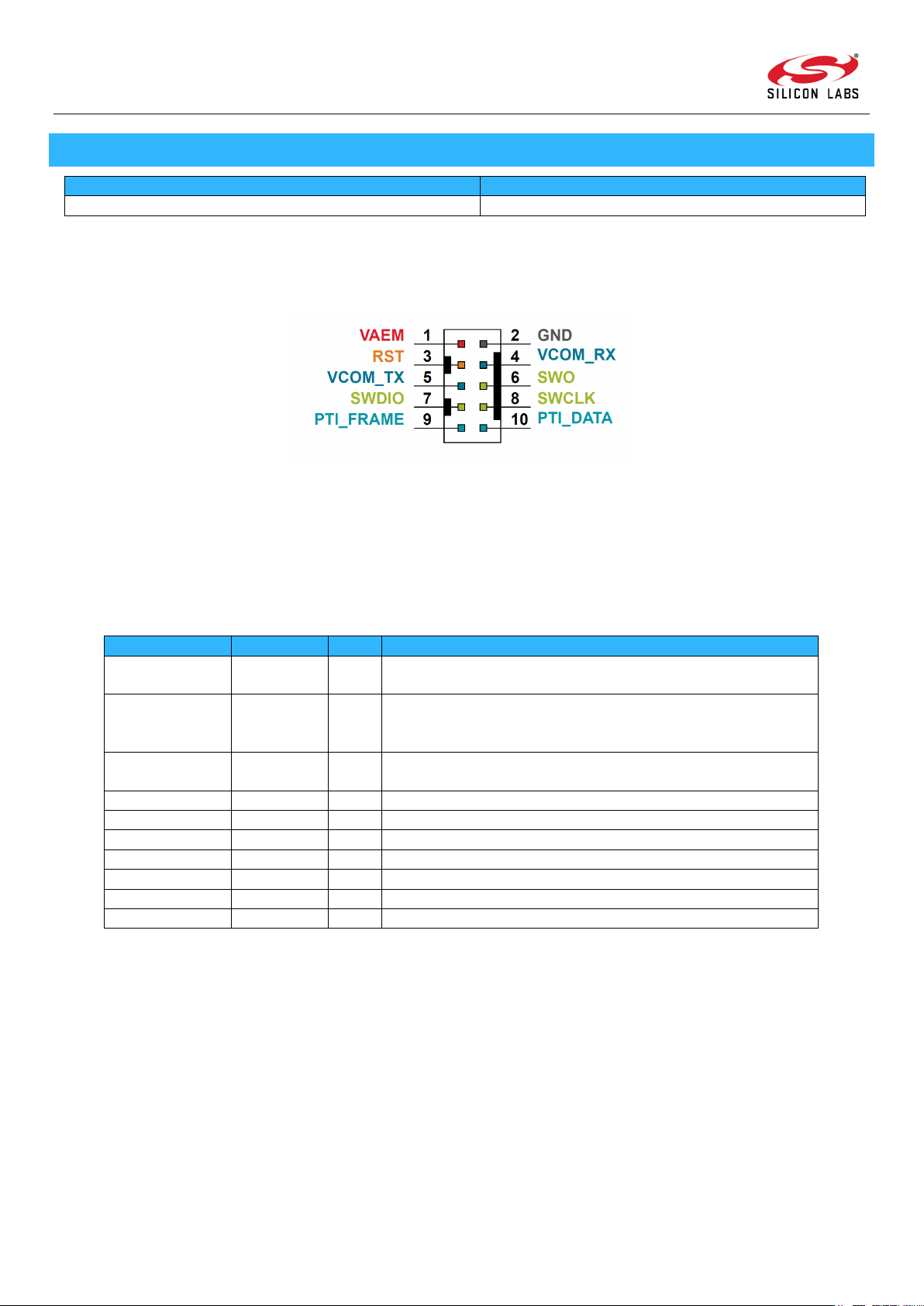
Figure 3.1: Silicon Labs Mini Simplicity Header
Pin Name
Pin Location
Type
Function
GND 2 S
Common ground between the programmer and Z-Wave 700
device
VAEM
1
S
Target voltage on the debugged application. Supplied and
"AEM" position.
RST 3 O
Driven low by the programmer to place the Z-Wave 700 device in
a reset state
VCOM_TX
5
I
Receive UART serial data from Z-Wave 700 device
VCOM_RX
4
O
Transmit UART serial data to Z-Wave 700 device
SWO
6
I
Serial Wire Output
SWDIO
7
I/O
Serial Wire Data
SWCLK
8
O
Serial Wire Clock
PTI_FRAME
9
I
Packet Trace Frame Signal
PTI_DATA
10
I
Packet Trace Data Signal
3 PROGRAMMING AND DEBUGGING INTERFACE
A programming interface is mandatory if In-System Programming of a Z-Wave 700 device is required, i.e., programming while
soldered onto the product PCB. To design in a footprint for the Mini Simplicity header, Silicon Labs recommends using a small 10pin 1.27 mm SMD header for both programming and debugging of chips from the Silicon Labs Gecko family.
If a connector is used, the Samtec FTSH-105-01-F-DH surface mounted or Harwin M50-3500542 through-hole male connector is
recommended and can be directly used with the
programmer’s perspective is shown in Table 3.1. Refer to [2] and [6] for programming instructions and more about the Mini
Simplicity Header.
BRD8010A STK/WSTK Debug Adapter. The functionality of the pins from the
Table 3.1: Z-Wave 700 Mini Simplicity Header Pin Functionality
monitored by the AEM when power selection switch is in the
INS14487-6 | 3/2021 3
Page 4
Instruction: Z-Wave Z-Wave 700 Integration Guide
SWD programming
X
X
Boot Loader UART programming
X
X
EFR32ZG14
ZGM130S
Applicable
N/A
EFR32ZG14
ZGM130S
Applicable
Applicable
3.1 PROGRAMMING INTERFACE OVERVIEW
The table below shows which interfaces can be used to program the flash memory of the various Z-Wave 700 products:
Table 3.2: Available Programming Interfaces
ZGM130S
4 CALIBRATION
It is mandatory to calibrate the crystal in EFR32ZG14 Z-Wave 700 devices during product development to make sure that the mean
value of the crystal frequency is correct. Refer to [5] for calibration instructions. Furthermore, for best possible performance, it is
recommended that calibration be performed during production to minimize the spread in crystal frequency. All ZGM130S Z-Wave
700 devices are calibrated during production and therefore do not need any further crystal calibration.
EFR32ZG14
4.1 CRYSTAL
It is mandatory to calibrate the crystal frequency for the EFR32ZG14 devices to ensure minimum error of the radio carrier
frequency.
5 RF VERIFICATION TOOL
The RailTest tool can be used to verify the RF performance of a device without the overhead of the Z-Wave protocol. The RailTest
tool supports both ZGM130S and EFR32ZG14 devices. The same RF PHY present in the Z-Wave protocol is used. The tool is suitable
when investigating RF performance and performing RF regulatory tests. To use the tool, it is required that the chip is
programmable and the UART0 interface is connected to a terminal over RS-232 or through the WSTK. For a comprehensive user’s
manual for the RailTest tool, refer to [3] and [4].
As the RF PHY can be updated for new software releases, it is important to compile a RailTest version based on the same software
release that will be used in the final product.
4 INS14487-6 | 3/2021
Page 5

Instruction: Z-Wave 700 Integration Guide
6 COMPONENT SPECIFICATIONS
6.1 SAW FILTER
EFR32ZG14 ZGM130S
Applicable Applicable
It is recommended that a SAW filter is used in Z-Wave 700 gateway designs also containing GSM or LTE transceivers operating in
the sub-GHz band. A SAW filter attenuates unwanted radio emissions and improves the receiver blocking performance. Three
regions are defined to cover the global Z-Wave frequency range. The SAW filter specifications described in Table 6.1, Table 6.2,
and Table 6.3 are recommended for new designs. An overview of supported Z-Wave regions and frequencies can be found in [1].
Please find a guideline on when to use a SAW filter in [15].
INS14487-6 | 3/2021 5
Page 6
Instruction: Z-Wave Z-Wave 700 Integration Guide
Frequency Range
Unit
Minimum
Typical
Maximum
Operating temperature
-
◦
C
-30 - +85
Insertion loss
865.0 to 870.1MHz
dB - -
3.5
Amplitude ripple
865.0 to 870.1MHz
dB - -
2.0
Relative attenuation
0.1 to 800.0MHz
dB
40 - -
805 to 830MHz
dB
35 - -
835 to 855MHz
dB - - - 860 to 862MHz
dB - -
-
890 to 1000MHz
dB
40 - -
1005 to 2000MHz
dB
30 - -
2005 to 3000MHz
dB
30 - -
3005 to 4000MHz
dB
30 - -
4005 to 6000MHz
dB - -
-
In / out impedance
-
Ω
-
50
-
Frequency Range
Unit
Minimum
Typical
Maximum
Operating temperature
-
◦
C
-30 - +85
Insertion loss
908.2 to 916.3MHz
dB - -
2.5
Amplitude ripple
908.2 to 916.3MHz
dB - -
1.5
Relative attenuation
720 to 800MHz
dB
45 - -
805 to 840MHz
dB - - - 845 to 870MHz
dB
40 - -
870 to 895MHz
dB - - - 940 to 1000MHz
dB 9 - - 1005 to 2000MHz
dB 9 - - 2005 to 3000MHz
dB
17 - -
3005 to 4000MHz
dB - - - 4005 to 6000MHz
dB - -
-
In / out impedance
-
Ω
-
50
-
Frequency Range
Unit
Minimum
Typical
Maximum
Operating temperature
-
◦
C
-30 - +85
Insertion loss
919.5 to 926.5MHz
dB - -
3.2
Amplitude ripple
919.5 to 926.5MHz
dB - -
1.0
Relative attenuation
40 to 870MHz
dB
40 - -
875 to 885MHz
dB
35 - -
890 to 905MHz
dB
20 - -
945 to 955MHz
dB
20 - -
960 to 1000MHz
dB
20 - -
1005 to 1500MHz
dB
40 - -
1505 to 3000MHz
dB
20 - -
3005 to 4000MHz
dB - - - 4005 to 6000MHz
dB - -
-
In / out impedance
-
Ω
-
50
-
Table 6.1: Region E
Table 6.2: Region U
6 INS14487-6 | 3/2021
Table 6.3: Region H
Page 7
Instruction: Z-Wave 700 Integration Guide
Region
Distributor
Component Number
Note
E
ACTE A/S, www.acte.dk, salessupport@acte.dk
SF4000-868-07-SX
Preferred
U
ACTE A/S, www.acte.dk, salessupport@acte.dk
SF4000-914-06-SX
Preferred
H
ACTE A/S, www.acte.dk, salessupport@acte.dk
SF1256-923-02
Preferred
Region
Distributor
Component Number
Note
E
ACTE A/S, www.acte.dk, salessupport@acte.dk
SF4000-869-14-SX
Improved LTE rejection
Region
State of PB14
State of PB15
E
High
Low U Low
High
H
Low
Low
EFR32ZG14
ZGM130S
Applicable
NA
6.1.1 RECOMMENDED COMPONENTS FOR GSM/LTE GATEWAYS
Table 6.4: SAW filters
6.1.2 OPTIONAL COMPONENTS FOR GSM/LTE GATEWAYS
Table 6.5: LTE improved SAW filters
6.1.3 Z-WAVE PROTOCOL SUPPORT FOR OPTIONAL SAW FILTER BANK
The Z-Wave Protocol offers support for usage of a SAW filter bank. Please refer to the BRD4200A and BRD4201A reference designs
for an example of such a SAW filter bank implementation.
Two GPIO pins on the Z-Wave 700 devices, GPIO PB14 and GPIO PB15 are assigned to control the selection of which SAW filter to
use in the SAW filter bank :
Table 6.6: SAW Filter Control Pins
6.2 CRYSTAL
The crystal is part of the oscillator that generates the reference frequency for the digital system clock and RF carrier. It is a critical
component of a Z-Wave 700 device. Further, it is mandatory to calibrate the crystal for EFR32ZG14-based designs. Refer to section
4 for more information.
The EFR32ZG14 has internal crystal capacitors and does not need any external circuitry apart from the crystal itself.
INS14487-6 | 3/2021 7
Page 8
Instruction: Z-Wave Z-Wave 700 Integration Guide
Parameter
Symbol
Min
Typ
Max
Unit
Crystal frequency
fHFXO
—
39 — MHz
Supported crystal equivalent series resistance
(ESR)
ESRHFXO_39M
— — 60
Ω
Supported range of crystal load capacitance 1
CHFXO_CL
6 — 12
pF
Initial frequency tolerance for the crystal
FTHFXO
-10 10
ppm
Temperature tolerance for the crystal
FTempHFXO
-40°C - 85°C
-12 12
ppm
Aging
FAge
-3 3
ppm/5yr
Combined tolerance for the crystal
FTtotalHFXO
-25 — 25
ppm/5yr
Manufacturer
Component Number
EOL issued
TXC
8Y39072002
C3
10U
R1
0R
GND
VBAT
C1
100N
C2
100N
VBAT_IN
EFR32ZG14
ZGM130S
Applicable
Applicable
The ZGM130S has an integrated crystal and is calibrated at the time of production.
For more information about the crystal oscillator, crystals and the EFR32ZG14 device, please refer to [7].
Table 6.7: Crystal specification for Z-Wave 700 devices
6.2.1 RECOMMENDED COMPONENTS
Table 6.8: Recommended crystals
7 SUPPLY FILTER
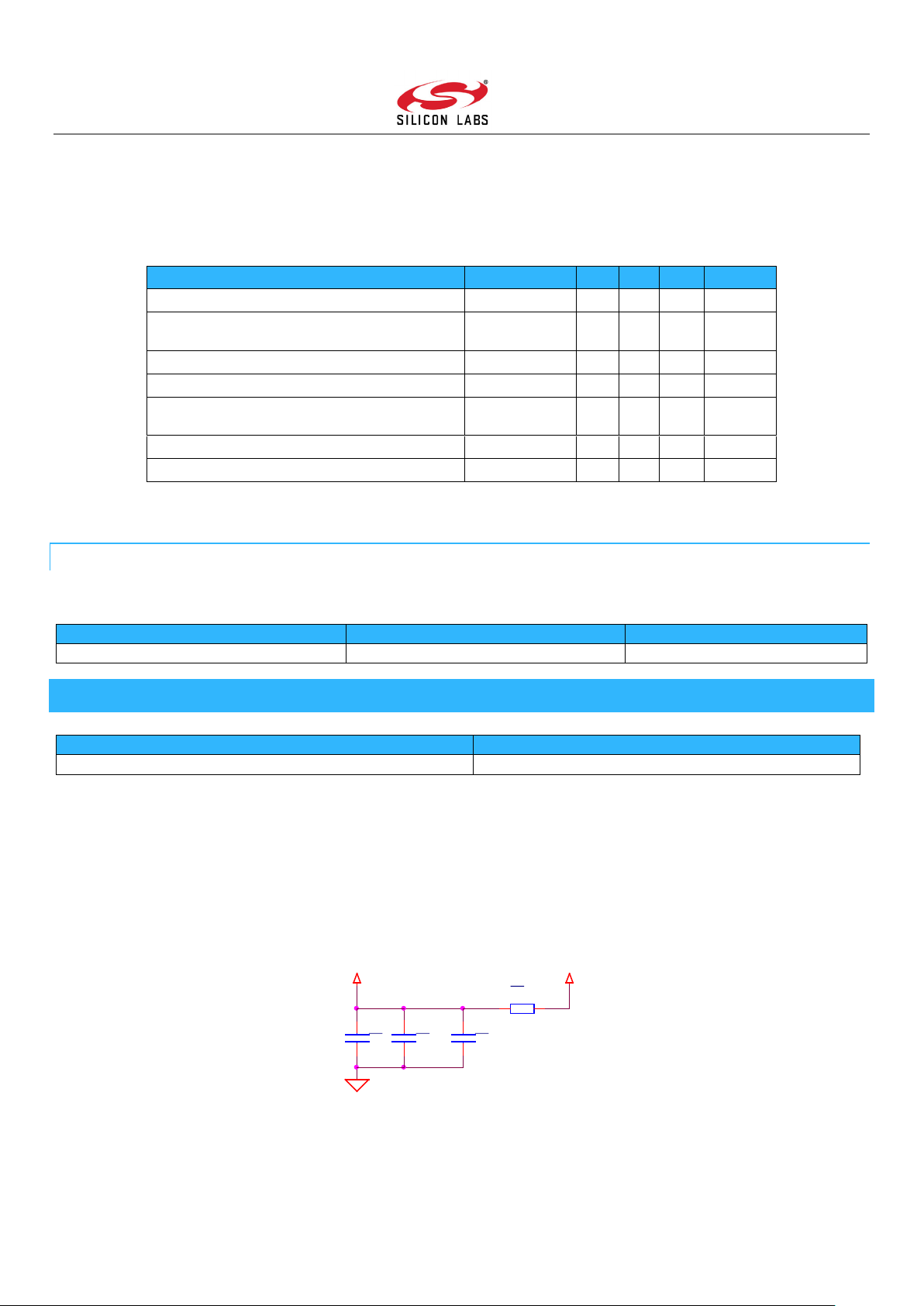
A good power supply filter is strongly recommended as part of the schematic. A filter with a ferrite and a capacitor can be used as
seen in Figure 8.1. The ferrite suppresses high frequency noise, while the capacitors decouple the power supply by acting as a
source for fast transient currents.
For Z-Wave 700 devices, the filter shown in Figure 7.1 is strongly recommended. For normal scenarios, this will provide adequate
filtering with a low BOM cost. In case of excessive supply noise, the 0 Ω resistor can be swapped for a ferrite bead to improve
filtering.
For more about supply decoupling, please refer to section 9.4. More in-depth information about decoupling strategies and the
Figure 7.1: Recommended Supply Filter for Z-Wave 700 Devices
power supply system of the Z-Wave devices can be found in [8] and [9].
8 INS14487-6 | 3/2021
Page 9

Instruction: Z-Wave 700 Integration Guide
General Z-Wave
Z-Wave Long Range
EFR32ZG14
ZGM130S
EFR32ZG14
ZGM130S
Matching
IPD + DC-blocking cap
DC blocking cap
Discrete match with ceramic
DC blocking cap
Matching
IPD + DC-blocking cap
DC blocking cap
Discrete match with ceramic
TX/RX path
DC blocking cap
Max. power
for US
-1 dBm
-1 dBm
14 dBm
14 dBm
Max. power
for EU
14 dBm
14 dBm
N/A
N/A
8 MATCHING CIRCUIT
The PA of the transmitter should be matched for maximum power transfer and the LNA of the receiver must be matched for
lowest noise. The matching is divided into the following operations:
1. Matching the SoC transceiver to a 50 Ω RF line on the PCB.
2. Additional filtering for Z-Wave Long Range.
3. Matching the 50 Ω RF line of the PCB to the antenna.
The first part is already done in the ZGM130S SiP and is therefore only applicable to the EFR32ZG14. The second part applies to
ZGM130S only when targeting Z-Wave Long Range. The third part must be done for all implementations unless a naturally matched
antenna like the ones on the BRD4206A or BRD4207A radio boards are used.
8.1 SUMMARY OF MATCHING + FILTERING NETWORKS
The recommended matching + filtering networks for General Z-Wave and Z-Wave Long Range can be found below:
Table 8.1: Z-Wave Recommended Matches
w/o SAW
w/SAW
The IPD and Discrete match with ceramic balun solutions are detailed in section 8.2.
+ SAW in TX/RX path
(BRD4201A)
(BRD4202A)
+ SAW in TX/RX
path (BRD4200A)
balun
+ 5-element Pi filter
(BRD4206A)
balun
+ 5-element Pi filter + SAW in
+ 3-element Pi filter
(BRD4207A)
+ SAW in TX/RX path
INS14487-6 | 3/2021 9
Page 10

Instruction: Z-Wave Z-Wave 700 Integration Guide
General Z-wave
Z-wave Long Range
EFR32ZG14
EFR32ZG14
Matching w/o SAW
Discrete match with ceramic balun
IPD + DC blocking cap
Full discrete match
Full discrete match
Matching w SAW
Discrete match with ceramic balun
IPD + DC-blocking cap
Max. power for US
-1 dBm
14 dBm
Max. power for EU
14 dBm
N/A
Alternatively, the following matching + filtering networks can be used for EFR32ZG14:
Table 8.2: Z-Wave Alternative Matches
+ 5-element Pi filter (Validated)
+ 5-element Pi filter (Tested)
+ 5-element Pi filter + SAW in TX/RX path (Validated)
The ‘Discrete match with ceramic balun + 5-element Pi filter’ is the same design that is present on BRD4206A. This solution is fully
characterized and validated.
The details about the ‘Full discrete match + 5-element Pi filter’ can be found in [16] section 3. This matching network has not been
validated yet but has been optimized on prototype PCBs.
The Murata LFD21868MMF5E233 IPD is recommended for General Z-Wave for EFR32ZG14 but can be used for Z-Wave Long Range
as well if an additional 3-element Pi filter is connected after the IPD for improved harmonic suppression. The proper component
values for the 3-element Pi filter can be found on Figure 8.3.
+ 3-element Pi filter (Tested)
+ 5-element Pi filter (Tested)
+ SAW in TX/RX path (Tested)
8.2 SOC TO RF LINE MATCHING
EFR32ZG14 ZGM130S
Applicable NA
The EFR32ZG14 has separate differential LNA input and PA outputs and will therefore require both balun and matching externally.
The recommended matching network for General Z-Wave with EFR32ZG14 is the Murata LFD21868MMF5E233 IPD, which matches
the EFR32ZG14 PA to the 50 Ω RF line as shown in Figure 8.1. This gives an easy and clean RF design with a very compact footprint
with only the IPD, two decoupling capacitors, and a ferrite for suppressing high frequency noise on the supply for the PA.
10 INS14487-6 | 3/2021
Page 11

Instruction: Z-Wave 700 Integration Guide
Sub-GHz
matching
network
C106
220N
U2
LFD21868MMF5E233
TXP
9
R XP
7
R XN
6
TXN
8
GND2
3
GND1
1
ANT
2
GND3
4
GND4
5
VDD
10
VDCDC
RF I/O
SUBGRF _OP
9
SUBGRF _ON
10
SUBGRF_IP
11
SUBGRF_IN
12
GND
L103
BLM03AX241SN1D
GND
50R_RF _OUT
C107
56P
Figure 8.1: Recommended RF Matching Component for the EFR32ZG14 SoC for General Z-Wave:
Murata LFD21868MMF5E233 IPD
The Murata part LFD21868MMF5E233 used for EFR32ZG14 circuits covers all supported Z-Wave regions and frequencies. The
IPD contains a matching network, a balun, and harmonic filtering as well, which provides sufficient harmonic suppression for
General Z-Wave applications.
For more in-depth knowledge about the IPD component and IPD’s in general, please refer to [13] and [14].
It is mandatory to connect the VDD pin of the IPD (U2) as shown in Figure 8.1. Connecting the VDD pin of the IPD to e.g. 3.3V is
not supported.
Z-Wave Long Range requires stronger harmonic suppression in the RF front-end, which the LFD21868MMF5E233 itself cannot
provide. For Z-Wave Long Range the recommended matching network is a discrete match combined with a ceramic balun and a
5-element low-pass filter:
Figure 8.2: Recommended Matching Network for the EFR32ZG14 SoC for Z-Wave Long Range
INS14487-6 | 3/2021 11
Page 12

Instruction: Z-Wave Z-Wave 700 Integration Guide
Manufacturer
Component Number
EOL issued
Murata
LFD21868MMF5E233
Manufacturer
Component Number
EOL issued
Johanson Technology
0900BL15C050
EFR32ZG14
ZGM130S
NA
Applicable
The matching network shown on Figure 8.2 used for EFR32ZG14 circuits is mainly recommended for Z-Wave Long Range but can
be used for General Z-Wave applications and other Z-Wave regions as well. The circuit contains a match to 50 Ω, a differential to
a single-ended balun, and a 5-element harmonic filtering network.
It is mandatory to connect the VDD pin of the balun (BAL1) as shown in Figure 8.2. Connecting the VDD pin of the balun (and the
EFR32ZG14 PA) to, e.g. 3.3V, is not supported.
For more in-depth knowledge about matching circuits, please refer to [10].
8.2.1 MANDATORY COMPONENTS FOR GENERAL Z-WAVE
Table 8.3: IPD
8.2.2 MANDATORY COMPONENTS FOR Z-WAVE LONG RANGE
Table 8.4: Balun
8.3 ADDITIONAL FILTERING FOR Z-WAVE LONG RANGE
ZGM130S has the matching and filtering network built-in, which provides acceptable harmonic performance for all Z-Wave regions
when targeting General Z-Wave. However, Z-Wave Long Range allows higher transmit power, therefore, additional harmonic
filtering is necessary. The following 3-element Pi filter should be connected to ZGM130S RF_ANT pin besides the DC blocking
capacitor (C11) when targeting Z-Wave Long Range.
Figure 8.3: Recommended Three-Element Pi Filter
12 INS14487-6 | 3/2021
Page 13

Instruction: Z-Wave 700 Integration Guide
RF_line
ANTENNA
1
R2
0R
GND
R1
0R
NM
R3
0R
NM
GND
8.4 RF LINE TO ANTENNA MATCHING
EFR32ZG14 ZGM130S
Applicable Applicable
Finding appropriate values for the components should be considered an iterative task. It is recommended to add a pi network for
matching as shown in Figure 8.4. The following matching strategy is proposed:
1. Calibrate your Vector Network Analyzer (VNA) for a frequency range larger than the intended bandwidth of the antenna.
2. Connect an RF coaxial cable to the RF line (for instance by soldering a pigtail to the line). Connect the RF coaxial cable to
a VNA to measure the reflection coefficient, S11, looking into the antenna through the matching network.
a. Be sure to have a good connection to the ground plane to get the best electrical performance and the highest
mechanical robustness during the measurement.
b. Make sure to route the pigtail towards the center of the PCB and then perpendicularly away from the PCB at the
center point. This will limit the effect of the cable on the measured data as much as possible.
3. Start out with no components on the antenna network shown in Figure 8.4:
a. The shunt components are not mounted.
b. The series component is not mounted.
4. Use line extension on the VNA to move the reference point to the footprint of R1 and R2.
a. This is achieved when the locus of the S-parameters in the Smith chart on the VNA have assembled in a point at
the right edge of the Smith chart.
5. Mount a 0 Ω resistor at R2 in Figure 8.4
6. Measure reflection coefficient for the frequency of interest (the frequency half way between the lowest frequency and
the highest frequency of the region of interest).
7. Use an online matching tool to calculate series and shunt component values to achieve 50 Ω match on the coaxial line.
a. This will give a good starting point and should result in a reasonably good match at first attempt.
8. Iteratively change component values until match is acceptable.
a. The standard matching criterion is either -6 dB or -10 dB reflection across all frequencies of interest.
b. When this goal is achieved, it is recommended to use the same values on a small sample of boards to make sure
that the matching is acceptable across production tolerances.
Figure 8.4: Recommended Antenna Matching Pi Network
A description of various antenna topologies can be found in [11]. Please also refer to the reference designs BRD4206A, BRD4207A,
and UZB7 for various methods of antenna implementations.
INS14487-6 | 3/2021 13
Page 14

Instruction: Z-Wave Z-Wave 700 Integration Guide
DUT Spectrum Analyzer
10
dB Attenuator
DUT
Z-Wave Frame
Generator
Attenuator
Variable Attenuator
1dB Steps
EFR32ZG14
ZGM130S
Applicable
Applicable except section 9.6
8.5 MEASUREMENT SETUP
The output power should be measured with a spectrum analyzer as shown in Figure 8.5 and sensitivity as shown in Figure 8.6. In
both cases, place the fixed attenuator as close as possible to the transmitter. The fixed attenuator prevents RF reflections in the
measurement setup.
Figure 8.5: Measuring Transmitter Output Power
When measuring the sensitivity, first measure and record the output power of the Z-Wave frame generator using the spectrum
analyzer. A Z-Wave 700 module programmed with the RailTest tool can be used as the Z-Wave frame generator. Then a fixed
attenuator can be used along with a variable attenuator to adjust the input power of the DUT. For example, by setting the output
power of the Z-Wave generator to -20dBm, a fixed 50dB attenuator and a variable 50dB attenuator can be used to measure the
sensitivity with a 1dB resolution. Place the fixed attenuator close to the Z-Wave generator and conduct the measurements in a
radio silent environment, e.g. by placing the DUT in a RF shielded box.
Figure 8.6: Measuring Receiver Sensitivity
9 PCB IMPLEMENTATION
A good PCB implementation is required to obtain the best performance from a Z-Wave 700 device. The following subsections
describe items that should be considered when designing the PCB layout.
Besides the descriptions below, please use the reference designs for the ZGM130S and the EFR32ZG14 devices as guidelines. The
reference designs for the ZGM130S are: BRD4200A, BRD4202A, and BRD4207A. The reference designs for the EFR32ZG14 are:
BRD4201A, BRD4206A, and UZB-7.
Further layout guidelines can be found in [12].
9.1 PLACEMENT
In general, it is mandatory that all decoupling and matching components are placed as close as possible to the Z-Wave 700 device,
and on the same layer to reduce trace parasitics. For gateway devices with GSM or LTE transceivers, it is also strongly
recommended to place the SAW filter as close as possible to the RF pin of the Z-Wave 700 device.
14 INS14487-6 | 3/2021
Page 15

Instruction: Z-Wave 700 Integration Guide
Prepreg
FR4
Prepreg
Signal
L1
L
2
L3
L4
Ground plane
Power and signal
Signal
Power in Power out
Low value capacitors High value capacitors
Via
Figure 9.3: Pin Decoupling
When implementing a Z-Wave system into a product, it is strongly recommended that the Z-Wave 700 device is placed close to a
corner of the product’s PCB, away from any high frequency switching circuits used elsewhere in the product, e.g. host CPU systems,
switching DC supplies, motor-controllers etc.
9.2 STACK-UP
If designing a product with the EFR32ZG14, it is recommended to use a 4-layer stack-up PCB as shown in Figure 9.1. The thickness
of the PCB stack-up can be chosen to optimize cost. It is strongly recommended that a solid copper plane be used as the ground
plane layer L2.
Figure 9.1: 4-layer stack-up
With the ZGM130S, the complex circuitry is contained inside the SiP. Therefore, there are good possibilities for making a cheap
two-layer PCB design with ZGM130S. This does require extra care in designing the RF routing, power supply, and ground layout as
no full-layer power and ground planes can be included.
Please refer to the BRD4206A and BRD4207A designs for more information.
9.3 POWER ROUTING
Use as short VDD traces as possible. The VDD trace can be a hidden, unwanted radiator so it is important to simplify the VDD
routing as much as possible and use large, continuous GND pours with many stitching vias. To achieve the simplified VDD routing,
try to avoid star topology of VDD traces (i.e., avoid connecting all VDD traces in one common point).
Please consider using the reference designs BRD4206A and BRD4207A as the reference designs when creating the power routing.
9.4 DECOUPLING
Power should be driven through decoupling capacitors to prevent parasitic inductances as shown in Figure 9.3. At least two
grounding vias is recommended for each component as shown in Figure 9.2.
Figure 9.2: Grounded Components
9.4.1 FOR ZGM130S SIP MODULE
For the ZGM130S, most of the decoupling is built in. This includes all supply decoupling except for two 10 µF capacitors, one on
AVDD and one on VDD and VDDIO combined.
INS14487-6 | 3/2021 15
Page 16

Instruction: Z-Wave Z-Wave 700 Integration Guide
Signal L1
L2Ground plane
Prepreg
Ground pour
Impedance
controlled trace
Ground pour
GND
C103
56P
VDCDC
Ground
RF Analog Power
RFVDD
5
RFVSS
13
C102
220N
GND
GND
GND
C116
10N
VDCDC
GND
GND
VMC U
GND
GND
C115
4U7
L100
4U7
C118
2U2
VMC U
GND
DC/DC Regulator
Analog Supply
I/O Supply
Reset
Ground
Digital Supply
Digital Logic
Digital Regulator
U1C
EFR32Z G14
RESETn
8
DVDD
28
DECOU PLE
29
IOVDD
30
VSS_PAD
0
AVDD
22
VREGVDD
27
VREGSW
26
VREGVSS
25
RADI O_#RESET
C111
220N
C110
10U
C113
10N
C114
220N
GND
C117
10N
C112
10U
VMC U
Figure 9.4: Recommended External Supply Decoupling for the ZGM130S
9.4.2 FOR EFR32ZG14 SOC
For an EFR32ZG14 device, the decoupling topology shown in Figure 9.5 is strongly recommended.
Figure 9.5: Minimum Supply Decoupling Required for the EFR32ZG14 SoC
9.5 RF TRACE
For RF traces longer than λ/16 at the fundamental frequency, it is mandatory to design the trace as a transmission line with a 50Ω
characteristic impedance. A coplanar waveguide similar to Figure 9.6 is recommended for a transmission line on signal layer L1.
16 INS14487-6 | 3/2021
Figure 9.6: Coplanar Waveguide
Page 17

Instruction: Z-Wave 700 Integration Guide
Ground pour
Ground pour
Via
Impedance controlled trace
Via
Applicable
Applicable
A via fence is recommended on both sides of a coplanar waveguide, as shown Figure 9.7, to short any return currents induced on
the top layer to ground.
Figure 9.7: Via Fence
A free tool, such as Saturn PCB Design Toolkit (http://www.saturnpcb.com/pcb_toolkit.htm
dimensions of the traces conveniently.
), can be used to calculate the
9.6 IC GROUNDING
QFN chips should be provided with a ground paddle with stitched-vias to minimize parasitic inductance and to provide a good
thermal heat sink as shown in Figure 9.8.
Figure 9.8: IC Ground Paddle
Please refer to the BRD4206A layout to see a practical implementation of a QFN footprint with exposed pad.
10 ANTENNA DESIGN
EFR32ZG14 ZGM130S
Since antenna design is very product dependent, it is mandatory to perform the antenna matching as described in Section 8.4.
Each product requires an individual antenna design for best power transfer and radiation characteristics.
The BRD4206A and BRD4207A radio boards example antenna designs are shown with naturally matched antennas not requiring
any lumped components.
INS14487-6 | 3/2021 17
Page 18

Instruction: Z-Wave Z-Wave 700 Integration Guide
EFR32ZG14
ZGM130S
Applicable
Applicable
11 ESD
Since ESD can destroy the Z-Wave 700 product, great care must be taken during manufacturing and assembly of final goods to
avoid ESD.
By design, all pins of EFR32ZG14 and ZGM130S are ESD protected up to a level of 2.5 kV HBM.
The ESD level of a SAW filter is typically << 2 kV HBM.
18 INS14487-6 | 3/2021
Page 19

Instruction: Z-Wave 700 Integration Guide
Abbreviation
Description
2FSK
2-key Frequency Shift Keying
2GFSK
2-key Gaussian Frequency Shift Keying
ACM
Abstract Control Model
ACMA
Australian Communications and Media Authority
ADC
Analog-to-Digital Converter
AES
Advanced Encryption Standard
API
Application Programming Interface
APM
Auto Programming Mode
AV
Audio Video
BALUN
Balanced to Unbalanced converter
BOD
Brown-Out Detector
CBC
Cipher-Block Chaining
CDC
Communications Device Class
CE
Conformité Européenne
COM
Communication
CPU
Central Processing Unit
CRC
Cyclic Redundancy Check
D
Differential
D-
Differential Minus
D+
Differential Plus
DAC
Digital-to-Analog Converter
DC
Direct Current
DMA
Direct Memory Access
DUT
Device Under Test
ECB
Electronic CodeBook
EMS
Electronic Manufacturing Services
EOL
End Of Life
ESD
Electro Static Discharge
ESR
Equivalent Series Resistance
FCC
Federal Communications Commission
FET
Field Effect Transistor
FER
Frame Error Rate
FLiRS
Frequently Listening Routing Slave
FR4
Flame Retardant 4
FSK
Frequency Shift Keying
GFSK
Gaussian Frequency Shift Keying
GP
General Purpose
GPIO
General Purpose Input Output
HBM
Human Body Model
I
Input
I/O
Input / Output
IC
Integrated Circuit
IDC
Insulation-Displacement Connector
IF
Intermediate Frequency
IGBT
Insulated-Gate Bipolar Transistor
INT
Interrupt
IPC
Interconnecting and Packaging Circuits
IPD
Integrated Passive Device
IR
Infrared
IRAM
Indirectly Addressable Random Access Memory
12 ABBREVIATIONS
INS14487-6 | 3/2021 19
Page 20

Instruction: Z-Wave Z-Wave 700 Integration Guide
Abbreviation
Description
ISM
Industrial, Scientific, and Medical
ISP
In-System Programming
ITU
International Telecommunications Union
JEDEC
Joint Electron Device Engineering Council
LED
Light-Emitting Diode
LNA
Low-Noise Amplifier
LO
Local Oscillator
lsb
Least Significant Bit
LSB
Least Significant Byte
MCU
Microcontroller Unit
MIC
Ministry of Internal affairs and Communications, Japan
MISO
Master In, Slave Out
MOSI
Master Out, Slave In
msb
Most Significant Bit
MSB
Most Significant Byte
NA
Not Applicable
NMI
Non-Maskable Interrupt
NRZ
Non-Return-to-Zero
NVM
Non-Volatile Memory
NVR
Non-Volatile Registers
O
Output
OEM
Original Equipment Manufacturer
OFB
Output FeedBack
OTP
One-Time Programmable
PA
Power Amplifier
Pb
Lead
PCB
Printed Circuit Board
PHY
L1 Physical Layer
POR
Power-On Reset
PWM
Pulse Width Modulator
QFN
Quad-Flat No-leads
RAM
Random Access Memory
RF
Radio Frequency
RoHS
Restriction of Hazardous Substances
ROM
Read Only Memory
RS-232
Recommended Standard 232
RX
Receive
S
Supply
SAW
Surface Acoustic Wave
SCK
Serial Clock
SFR
Special Function Register
SiP
System-in-Package
SPI
Serial Peripheral Interface
SRAM
Static Random Access Memory
T0
Timer 0
T1
Timer 1
TX
Transmit
UART
Universal Asynchronous Receiver Transmitter
USB
Universal Serial Bus
VNA
Vector Network Analyzer
WUT
Wake-Up Timer
20 INS14487-6 | 3/2021
Page 21

Instruction: Z-Wave 700 Integration Guide
Abbreviation
Description
XRAM
External Random Access Memory
XTAL
Crystal
ZEROX
Zero Crossing
INS14487-6 | 3/2021 21
Page 22

Instruction: Z-Wave Z-Wave 700 Integration Guide
Date
Version
Affected
Revision
2018/11/26
1A
§All
Initial draft based on INS12213-15: "500 Series Integration Guide”
2018/12/3
1B
P. 1, 3-5, 7, 9, 14, 18
Updated based on comments from JFR and OPP
2018/12/4
1C
P. 4, 6, 14
Updated based on comments from NTJ and MHANSEN
2018/12/4
1D
§All
Table 6.6 added and all references to devices corrected to ‘Z-Wave 700’
2018/12/5
1E
P. 18
Legal disclaimer updated based on Silicon Labs disclaimer from AN961
2018/12/5
1F
Front page
Corrected title to "Z-Wave 700 Integration Guide"
2018/12/6
1G
Table 6.6
Corrected temp range (-40 °C – 85 °C) and removed size specification
2019/02/26
1H
§All
Added references, corrected language and clarified content.
2019/03/14
1I
Section 1,
6.1,6.1.3,8.1
Minor corrections and additions of references
2020/12/1
1J
All
Added support for Z-Wave Long Range
2021/03/10
1K
Section 6.1, Table
Changing ZGM130S to applicable for SAW filters, minor corrections in
Table 8.2
13 REVISION HISTORY
8.1, Table 8.2
Table 8.1 and Table 8.2, minor changes in content to reflect ZGM130S
usability as a gateway, removed Split TX / RX + RF Switch option from
22 INS14487-6 | 3/2021
Page 23

Instruction: Z-Wave 700 Integration Guide
14 REFERENCES
[1] https://www.silabs.com/products/wireless/mesh-networking/z-wave/benefits/technology/global-regions
[2] Silicon Labs, “Silicon Labs Production Programming Options”, AN136
[3] Silicon Labs, “Instruction for Bring-up/test HW development”, INS14283
[4] Silicon Labs, “AN972: EFR32 RF Evaluation Guide”, AN972
[5] Silicon Labs, “Instruction for Mandatory crystal adjustment for EFR32ZG14 based products”, INS14498
[6] Silicon Labs, “Debugging and Programming Interfaces for Custom Designs”, AN958
[7] Silicon Labs, “Oscillator Design Considerations”, AN0016.1
[8] Silicon Labs, “EFM32 and EFR32 Series 1 Power Configurations and DC-DC”, AN0948
[9] Silicon Labs, “EFM32 and EFR32 Wireless Gecko Series 1 Hardware Design Considerations”, AN0002.1
[10] Silicon Labs, “EFR32 Series 1 sub-GHz Matching Guide”, AN923.1
[11] Silicon Labs, “Antennas for Short Range Devices”, APL10045
[12] Silicon Labs, “EFR32 Series 1 Layout Design Guide”, AN928.1
[13] Silicon Labs, “Integrated Passive Devices for EFR32 Sub-GHz RF Matching”, AN1081
[14] Silicon Labs, “Murata 868 MHz IPDs for EFR32 Wireless SOCs”, AN1149
[15] Silicon Labs, “Z-Wave 700: SAW filter recommendations” :
wave/knowledge-base.entry.html/2019/01/16/z-wave_700_saw_filt-s5Ev
[16] Silicon Labs, “EFR32 Series 1 sub-GHz Discrete Matching Solutions”, AN1180
https://www.silabs.com/community/wireless/z-
INS14487-6 | 3/2021 23
Page 24

Instruction: Z-Wave Z-Wave 700 Integration Guide
DISCLAIMER
Silicon Labs intends to provide customers with the latest, accurate, and in-depth documentation of all peripherals and modules
available for system and software implementers using or intending to use the Silicon Labs products. Characterization data,
available modules and peripherals, memory sizes and memory addresses refer to each specific device, and "Typical" parameters
provided can and do vary in different applications. Application examples described herein are for illustrative purposes only. Silicon
Labs reserves the right to make changes without further notice and limitation to product information, specifications, and
descriptions herein, and does not give warranties as to the accuracy or completeness of the included information. Silicon Labs
shall have no liability for the consequences of use of the information supplied herein. This document does not imply or express
copyright licenses granted hereunder to design or fabricate any integrated circuits. The products are not designed or authorized
to be used within any Life Support System without the specific written consent of Silicon Labs. A "Life Support System" is any
product or system intended to support or sustain life and/or health, which, if it fails, can be reasonably expected to result in
significant personal injury or death. Silicon Labs products are not designed or authorized for military applications. Silicon Labs
products shall under no circumstances be used in weapons of mass destruction including (but not limited to) nuclear, biological
or chemical weapons, or missiles capable of delivering such weapons.
TRADEMARKS
Silicon Laboratories Inc.® , Silicon Laboratories®, Silicon Labs®, SiLabs® and the Silicon Labs logo®, Z-Wave®, Z-Wave Logo®,
Bluegiga®, Bluegiga Logo®, Clockbuilder®, CMEMS®, DSPLL®, EFM®, EFM32®, EFR, Ember®, Energy Micro, Energy Micro logo and
combinations thereof, "the world’s most energy friendly microcontrollers", Ember®, EZLink®, EZRadio®, EZRadioPRO®, Gecko®,
ISOmodem®, Micrium, Precision32®, ProSLIC®, Simplicity Studio®, SiPHY®, Telegesis, the Telegesis Logo®, USBXpress®, Zentri and
others are trademarks or registered trademarks of Silicon Labs. ARM, CORTEX, Cortex-M4 and THUMB are trademarks or
registered trademarks of ARM Holdings. Keil is a registered trademark of ARM Limited. All other products or brand names
mentioned herein are trademarks of their respective holders.
SALES OFFICE AND DISTRIBUTOR CONTACT INFORMATION
https://www.silabs.com/about-us/contact-sales
HEADQUARTERS
Silicon Laboratories Inc.
400 West Cesar Chavez
Austin, TX 78701
USA
www.silabs.com
24 INS14487-6 | 3/2021
 Loading...