

Page 1
UG336: Si5396J Evaluation Board User's
Guide
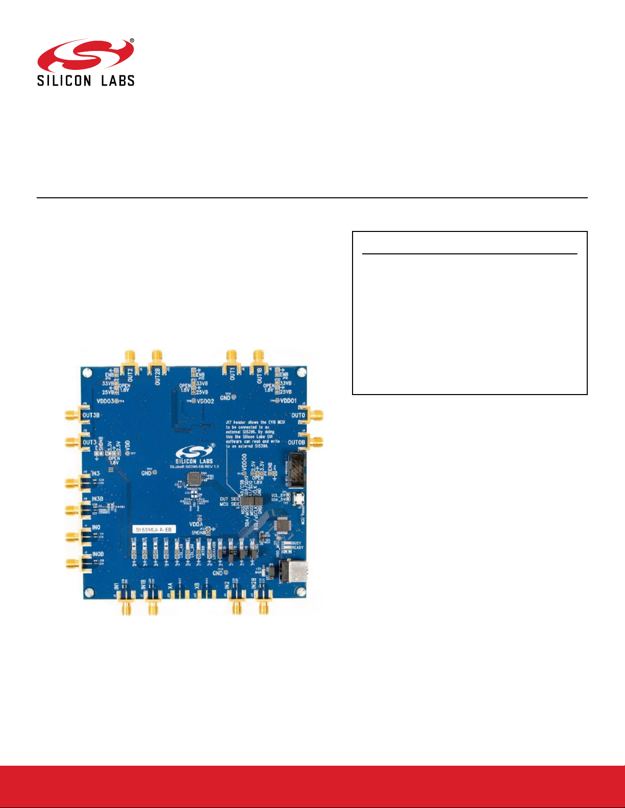
The Si5396J-A-EVB is used for evaluating the Si5396 Any-Frequency, AnyOuput, Jitter-Attenuating Clock Multiplier. There is only one EVB for the 44pin 4 output Si5396, which is an embedded reference device J-grade. There
is no EVB for the external reference A grade version for the Si5396-EVB.
The device grade and revision is distinguished by a white 1 inch x 0.187
inch label with the text “Si5396J-A-EB” installed in the lower left hand corner
of the board. (For ordering purposes only, the terms “EB” and “EVB” refer to
the board and the kit respectively. For the purpose of this document, the
terms are synonymous in context.)
KEY FEATURES OR KEY POINTS
• Si5396J-A-EVB for evaluating internal reference versions
Si5396J/K
•
Powered from USB port or external power supply.
•
ClockBuilder® Pro (CBPro) GUI programmable VDD
supply allows device to operate from 3.3, 2.5, or 1.8 V.
• CBPro GUI allows control and measurement of voltage,
current, and power of VDD and all 4 VDDO supplies.
• Status LEDs for power supplies and control/status
signals of Si5396J.
• SMA connectors for input clocks and output clocks
silabs.com | Building a more connected world. Rev. 1.1
Page 2

Table of Contents
Si5396J-A-EVB Functional Block Diagram ....................3
1.
2. Si5396J-A-EVB Support Documentation and ClockBuilder Pro Software .........4
3. Quick Start ................................5
4. Jumper Defaults ..............................6
5. Status LEDs................................7
6. Clock Input Circuits (INx/INxB) .........................8
7. Clock Output Circuits (OUTx/OUTxB) ......................9
8. External Reference Clock (XA/XB) Not Supported ................10
9. Installing ClockBuilder Pro Desktop Software ..................11
10. Using the Si5396J-A-EVB .........................12
10.1 Connecting the EVB to Your Host PC ......................12
10.2 Overview of ClockBuilder Pro Applications ....................13
10.3 Common ClockBuilder Pro Work Flow Scenarios ..................14
10.4 Workflow Scenario #1: Testing a Silicon Labs-Created Default Configuration ........15
10.4.1 Verify Free-Run Mode Operation ......................18
10.4.2 Verify Locked Mode Operation .......................20
10.5 Workflow Scenario #2: Modifying the Default Silicon Labs-Created Device
Configuration ..............................21
10.6 Workflow Scenario #3: Testing a User-Created Device Configuration ...........23
10.7 Exporting the Register Map File for Device Programming by a Host Processor ........26
11. Writing a New Frequency Plan or Device Configuration to Non-Volatile Memory (OTP) ..28
12. Serial Device Communications .......................29
12.1 Onboard SPI Support ...........................29
12.2 External I2C Support ...........................29
13. Si5396J-A-EVB Schematic and Bill of Materials (BOM) ..............30
14. Revision History............................. 31
silabs.com | Building a more connected world. Rev. 1.1 | 2
Page 3
UG336: Si5396J Evaluation Board User's Guide
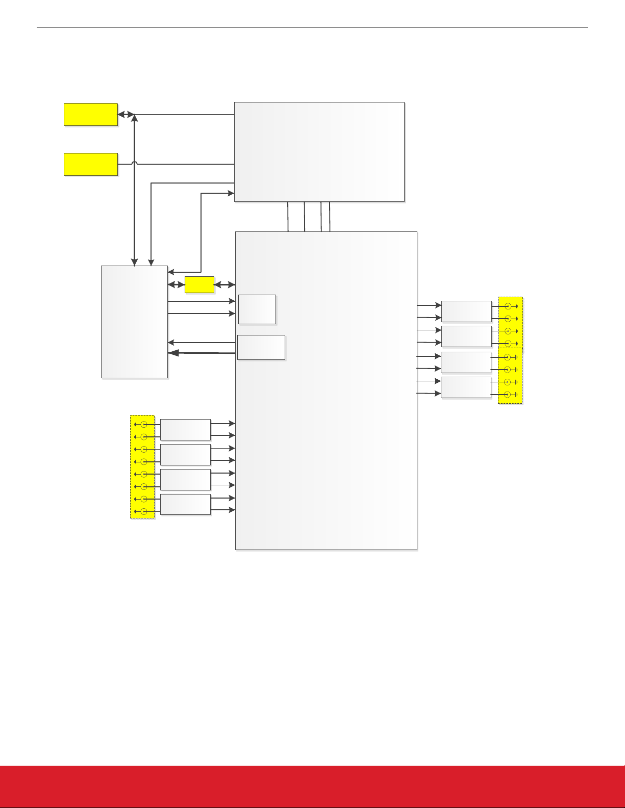
Si5396J-A-EVB Functional Block Diagram
1. Si5396J-A-EVB Functional Block Diagram
Below is a functional block diagram of the Si5396J-A-EVB. This evaluation board can be connected to a PC via the main USB connector for programming, control, and monitoring. See section 3. Quick Startor section 9. Installing ClockBuilder Pro Desktop Softwarefor
more information.
Main USB
Connector
USB Aux +5V
Connector
C8051F380
MCU
+
Peripherals
Power only
SPI
Conn
+5V_USB
+5V_Ext
VDDMCU
I2C
I2C/SPI Bus
Control/
Status
INTR
Alarm_Status
Power Supply
VDD_Core
VDD_Core
VDDO_0
VDD_3.3
VDDO_0
VDD_3.3
VDDO_1
VDDO_1
Si5396J
CLKOUT_0
CLKOUT_0B
CLKOUT_1
CLKOUT_1B
CLKOUT_2
CLKOUT_2B
CLKOUT_3
CLKOUT_3B
Output
Termination
Output
Termination
Output
Termination
Output
Termination
Output Clock 0
}
Output Clock 1
}
Output Clock 2
}
Output Clock 3
}
Input Clock 0
Input Clock 1
Input Clock 2
Input Clock 3
{
{
{
{
Input
Termination
Input
Termination
Input
Termination
Input
Termination
Figure 1.1. Si5396J-A-EVB Functional Block Diagram
CLKIN_0
CLKIN_0B
CLKIN_1
CLKIN_1B
CLKIN_2
CLKIN_2B
CLKIN_3
CLKIN_3B
silabs.com | Building a more connected world. Rev. 1.1 | 3
Page 4

UG336: Si5396J Evaluation Board User's Guide
Si5396J-A-EVB Support Documentation and ClockBuilder Pro Software
2. Si5396J-A-EVB Support Documentation and ClockBuilder Pro Software
All Si5396J-A-EVB schematics, BOMs, User’s Guides, and software can be found online:
www.silabs.com/documents/public/schematic-files/si539x-design-files.zip
silabs.com | Building a more connected world. Rev. 1.1 | 4
Page 5

UG336: Si5396J Evaluation Board User's Guide
3. Quick Start
1. Install ClockBuilder Pro desktop software from https://www.silabs.com/products/development-tools/software/clock.
2. Connect a USB cable from Si5396J-A-EB to the PC where the software was installed.
3. Confirm jumpers are installed as shown in Table 4.1 Si5396J-A-EVB Jumper Defaults on page 6.
4. Launch the ClockBuilder Pro Software.
5. You can use ClockBuilder Pro to create, download, and run a frequency plan on the Si5396-A-EB.
6. Find the Si5396J data sheet: https://www.silabs.com/documents/public/data-sheets/si5397-96-a-datasheet.pdf
Quick Start
silabs.com | Building a more connected world. Rev. 1.1 | 5
Page 6
4. Jumper Defaults
UG336: Si5396J Evaluation Board User's Guide
Jumper Defaults
Table 4.1. Si5396J-A-EVB Jumper Defaults
Location Type I = Installed
0 = Open
JP1 2 pin I
JP2 2 pin I
JP3 2 pin O
JP4 2 pin I
JP5 3 pin 1 to 2 (USB)
Note: Refer to the Si5396J-A-EVB schematics for the functionality associated with each jumper.
Location Type I = Installed
J17 5 x 2 Hdr All 5 installed
0 = Open
silabs.com | Building a more connected world. Rev. 1.1 | 6
Page 7
UG336: Si5396J Evaluation Board User's Guide
Status LEDs
5. Status LEDs
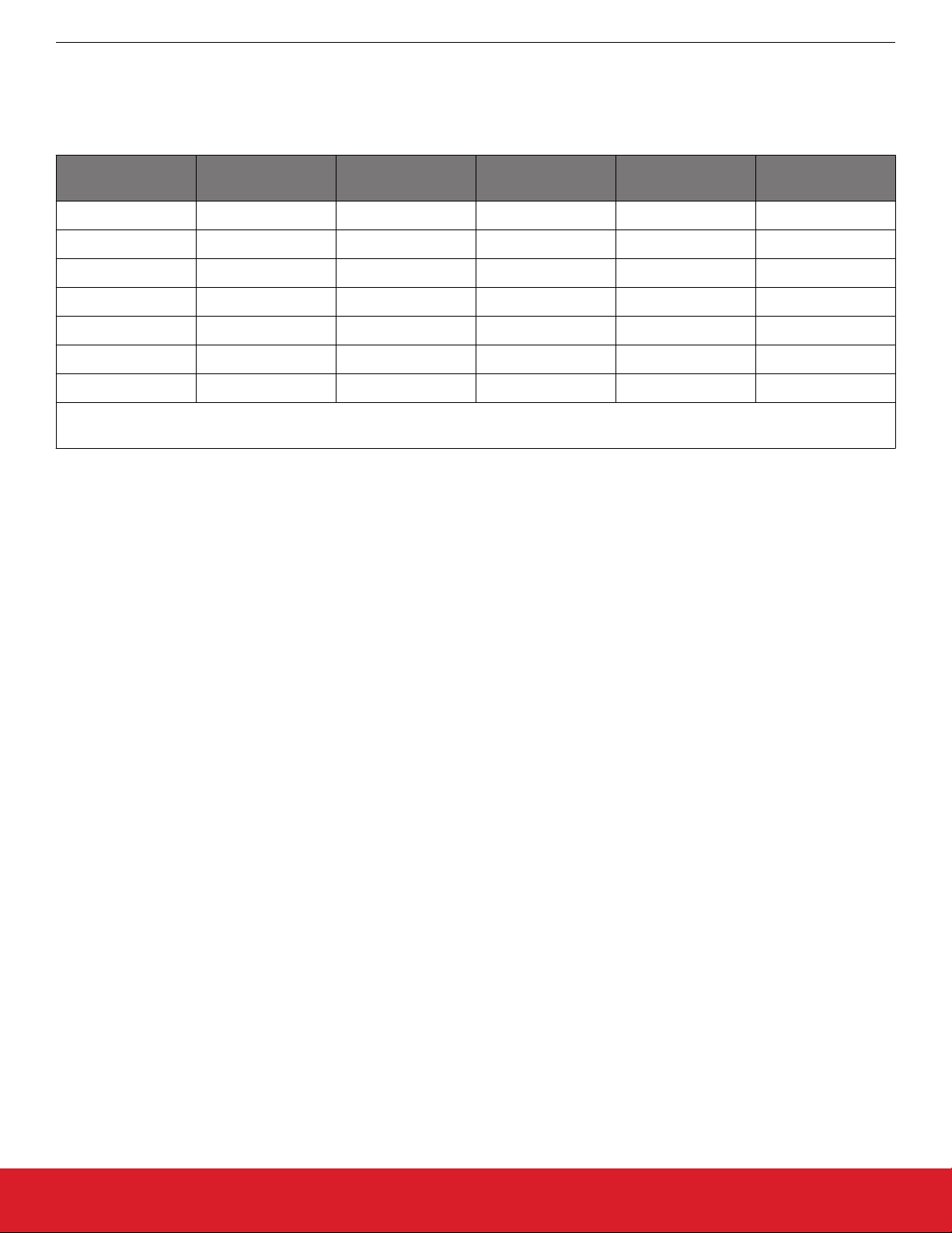
Table 5.1. Si5396J-A- EVB Status LEDs
Location Silkscreen Color Status Function Indication
D5 LOS_XAXBB Blue XA/XB Loss of Signal indicator
D6 INTRB Blue MCU INTR (Interrupt) active
D7 LOL_BB Blue DSPLL A Loss of Lock indicator
D8 LOL_AB Blue DSPLL B Loss of Lock indicator
D11 +5V MAIN Green Main USB +5V present
D12 READY Green MCU Ready
D13 BUSY Green MCU Busy
D5, D6, D7, and D8 are status LEDs indicating the device alarms currently asserted. D11 is illuminated when USB +5 V supply voltage
is present. D12 and D13 are status LEDs showing on-board MCU activity.
Figure 5.1. Status LEDs
silabs.com | Building a more connected world. Rev. 1.1 | 7
Page 8
UG336: Si5396J Evaluation Board User's Guide
Clock Input Circuits (INx/INxB)
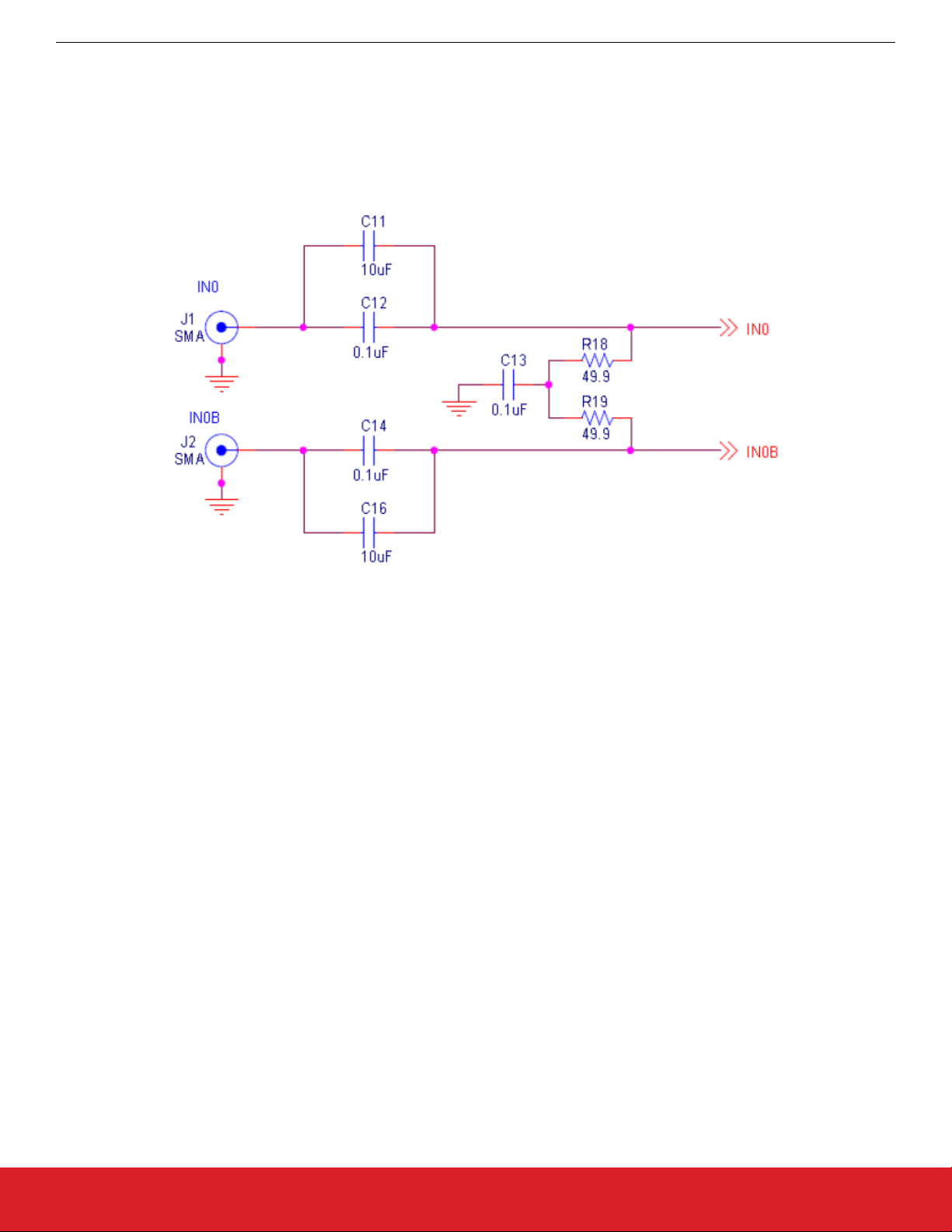
6. Clock Input Circuits (INx/INxB)
The Si5396J-A-EVB has eight SMA connectors (IN0/IN0B–IN3/IN3B) for receiving external clock signals. All input clocks are terminated
as shown in Figure 6.1 Input Clock Termination Circuit on page 8 below. Note input clocks are ac-coupled and 50 Ω terminated. This
represents four differential input clock pairs. Single-ended clocks can be used by appropriately driving one side of the differential pair
with a single-ended clock. For details on how to configure inputs as single-ended, please refer to the Si5396 data sheet. Typically a
0.1 μF dc block is sufficient, however, 10 μF may be needed for lower input frequencies. Note that the EVB is populated with both dc
block capacitor values.
Figure 6.1. Input Clock Termination Circuit
silabs.com | Building a more connected world. Rev. 1.1 | 8
Page 9
UG336: Si5396J Evaluation Board User's Guide
Clock Output Circuits (OUTx/OUTxB)
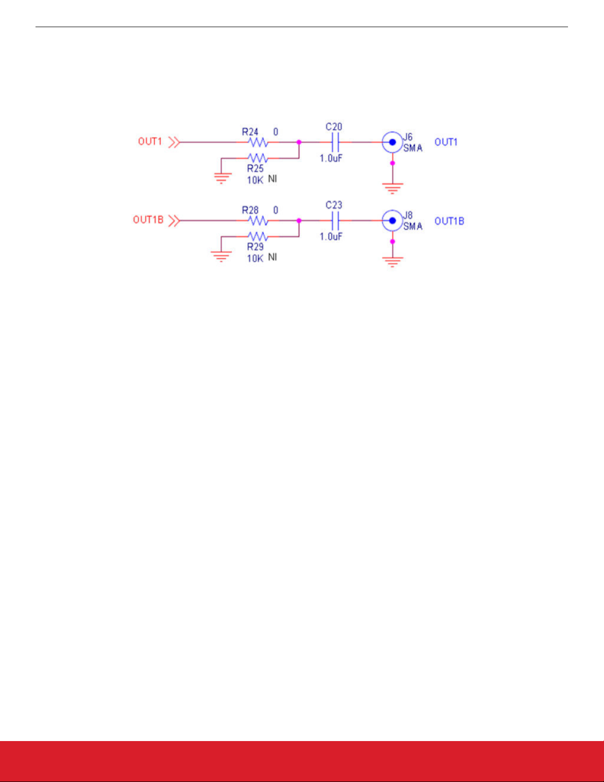
7. Clock Output Circuits (OUTx/OUTxB)
Each of the eight output drivers (four differential pairs) is ac-coupled to its respective SMA connector. The output clock termination circuit is shown in Figure 7.1 Output Clock Termination Circuit on page 9 below. The output signal will have no dc bias. If dc coupling is
required, the ac coupling capacitors can be replaced with a resistor of appropriate value. The Si5396J-A-EVB provides an L-network at
OUT0/OUT0B output pins for optional output termination resistors. Note that components with schematic “NI” designation are not normally populated.
Figure 7.1. Output Clock Termination Circuit
silabs.com | Building a more connected world. Rev. 1.1 | 9
Page 10
UG336: Si5396J Evaluation Board User's Guide
External Reference Clock (XA/XB) Not Supported
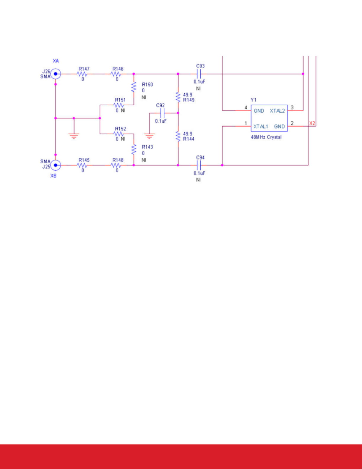
8. External Reference Clock (XA/XB) Not Supported
The Si5396J-A-EVB does not support an external reference clock on XA/XB. The layout for the external XTAL is on the board, but the
EVB for this part is an embedded XTAL version only and therefore this circuit should remain disconnected and unused.
Figure 8.1. External Reference Clock Termination Circuit
silabs.com | Building a more connected world. Rev. 1.1 | 10
Page 11

UG336: Si5396J Evaluation Board User's Guide
Installing ClockBuilder Pro Desktop Software
9. Installing ClockBuilder Pro Desktop Software
To install the CBOPro software on any Windows 7 (or above) PC:
Go to http://www.silabs.com/CBPro and download ClockBuilder Pro software.
Installation instructions and User’s Guide for ClockBuilder Pro can be found at the download link shown above. Please follow the instructions as indicated.
silabs.com | Building a more connected world. Rev. 1.1 | 11
Page 12
UG336: Si5396J Evaluation Board User's Guide
10. Using the Si5396J-A-EVB
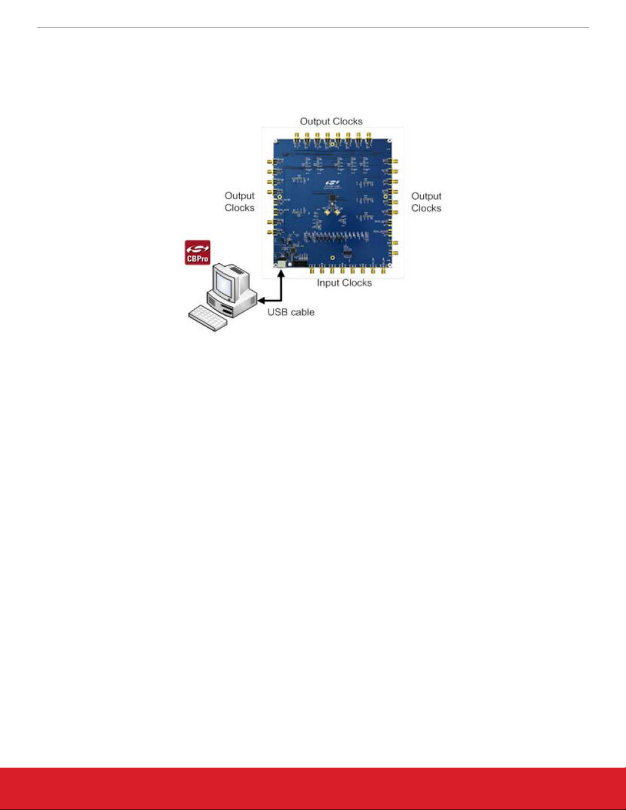
10.1 Connecting the EVB to Your Host PC
Once ClockBuilder Pro software is installed, connect to the EVB with a USB cable as shown below.
Using the Si5396J-A-EVB
Figure 10.1. EVB Connection Diagram
silabs.com | Building a more connected world. Rev. 1.1 | 12
Page 13
UG336: Si5396J Evaluation Board User's Guide
Using the Si5396J-A-EVB
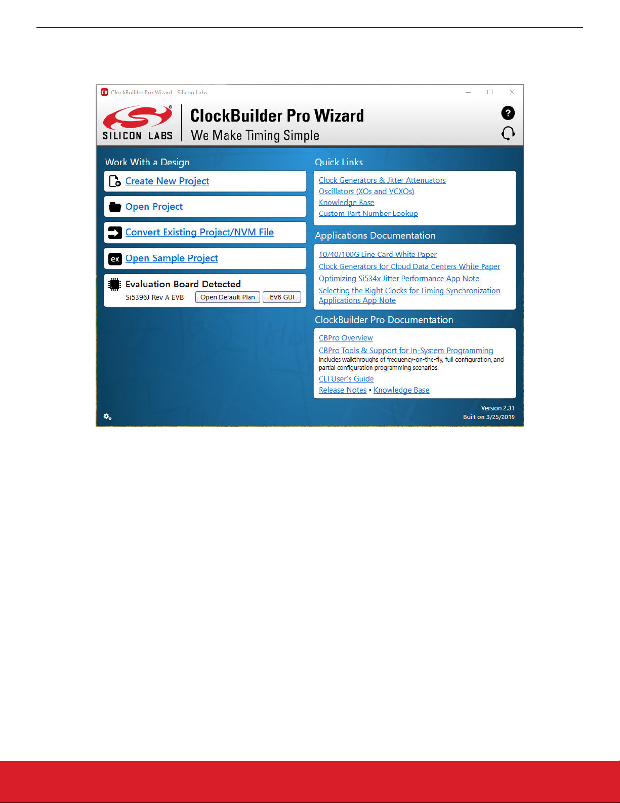
10.2 Overview of ClockBuilder Pro Applications
following instructions and screen captures may vary slightly depending on the version of ClockBuilder Pro. (The screen captures
The
below were taken for a board labeled "SI5396J-A-EB".) The ClockBuilder Pro installer will install two main applications:
Use the CBPro Wizard to:
• Create a new design
• Review or edit an existing design
• Export: create in-system programming
Figure 10.2. Application #1: ClockBuilder Pro Wizard
silabs.com | Building a more connected world. Rev. 1.1 | 13
Page 14

UG336: Si5396J Evaluation Board User's Guide
Using the Si5396J-A-EVB
Figure 10.3. Application #2: EVB GUI
Use the EVB GUI to:
• Download configuration to EVB’s DUT (Si5396)
• Control the EVB’s regulators
• Monitor voltage, current, power on the EVB
10.3 Common ClockBuilder Pro Work Flow Scenarios
There are three common workflow scenarios when using CBPro and the Si5396J-A-EVB. These workflow scenarios are:
• Workflow Scenario #1: Testing a Silicon Labs-Created Default Configuration
• Workflow Scenario #2: Modifying the Default Silicon Labs-Created Device Configuration
• Workflow Scenario #3: Testing a User-Created Device Configuration
Each is described in more detail in the following sections.
silabs.com | Building a more connected world. Rev. 1.1 | 14
Page 15
UG336: Si5396J Evaluation Board User's Guide
Using the Si5396J-A-EVB
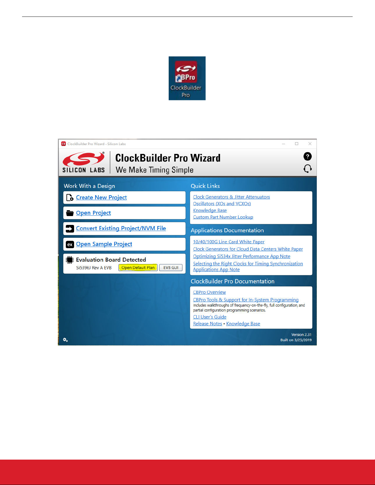
10.4 Workflow Scenario #1: Testing a Silicon Labs-Created Default Configuration
The flow for using the EVB GUI to initialize and control a device on the EVB is as follows.
Once the PC and EVB are connected, launch ClockBuilder Pro by clicking on this icon on your PC’s desktop.
Figure 10.4. ClockBuilder Pro Desktop Icon
If an EVB is detected, click on the “Open Default Plan” button on the Wizard’s main menu. CBPro automatically detects the EVB and
device type.
Figure 10.5. Open Default Plan
silabs.com | Building a more connected world. Rev. 1.1 | 15
Page 16

UG336: Si5396J Evaluation Board User's Guide
Using the Si5396J-A-EVB
Once you open the default plan (based on your EVB model number), a popup will appear.
Figure 10.6. Write Design to EVB Dialog
Select “Yes” to write the default plan to the Si5396 device mounted on your EVB. This ensures the device is completely reconfigured
per the Silicon Labs default plan for the DUT type mounted on the EVB.
Figure 10.7. Writing Design Status
After CBPro writes the default plan to the EVB, click on “Open EVB GUI” as shown below.
silabs.com | Building a more connected world. Rev. 1.1 | 16
Page 17

UG336: Si5396J Evaluation Board User's Guide
Using the Si5396J-A-EVB
Figure 10.8. Open EVB GUI
The EVB GUI will appear. Note all power supplies will be set to the values defined in the device default CBPro project file created by
Silicon Labs, as shown below.
Figure 10.9. EVB GUI Window
silabs.com | Building a more connected world. Rev. 1.1 | 17
Page 18

10.4.1 Verify Free-Run Mode Operation
UG336: Si5396J Evaluation Board User's Guide
Using the Si5396J-A-EVB
Assuming
no external clocks have been connected to the INPUT CLOCK differential SMA connectors (labeled “INx/INxB”) located
around the perimeter of the EVB, the DUT should now be operating in free-run mode, as the DUT will be locked to the crystal in this
case.
You can run a quick check to determine if the device is powered up and generating output clocks (and consuming power) by clicking on
the Read All button highlighted above and then reviewing the voltage, current and power readings for each VDDx supply.
Note: Shutting “Off” then “On” of the VDD and VDDA supplies will power-down and reset the DUT. Every time you do this, to reload the
Silicon Labs-created default plan into the DUT’s register space, you must go back to the Wizard’s main menu and select “Write Design
to EVB” as shown below.
Figure 10.10. Write Design to EVB
Failure to do the step above will cause the device to read in a pre-programmed plan from its non-volatile memory (NVM). However, the
plan loaded from the NVM may not be the latest plan recommended by Silicon Labs for evaluation.
At
this point, you should verify the presence and frequencies of the output clocks (running to free-run mode from the crystal) using appropriate external instrumentation connected to the output clock SMA connectors. To verify the output clocks are toggling at the correct
frequency and signal format, click on View Design Report as highlighted below.
silabs.com | Building a more connected world. Rev. 1.1 | 18
Page 19

UG336: Si5396J Evaluation Board User's Guide
Using the Si5396J-A-EVB
Figure 10.11. View Design Report
silabs.com | Building a more connected world. Rev. 1.1 | 19
Page 20

UG336: Si5396J Evaluation Board User's Guide
Using the Si5396J-A-EVB
Your configuration’s design report will appear in a new window, as shown below. Compare the observed output clocks to the frequencies and formats noted in your default project’s Design Report.
Figure 10.12. Design Report Window
10.4.2 Verify Locked Mode Operation
Assuming
you connect the correct input clocks to the EVB (as noted in the Design Report shown above), the DUT on your EVB will be
running in “locked” mode.
silabs.com | Building a more connected world. Rev. 1.1 | 20
Page 21

UG336: Si5396J Evaluation Board User's Guide
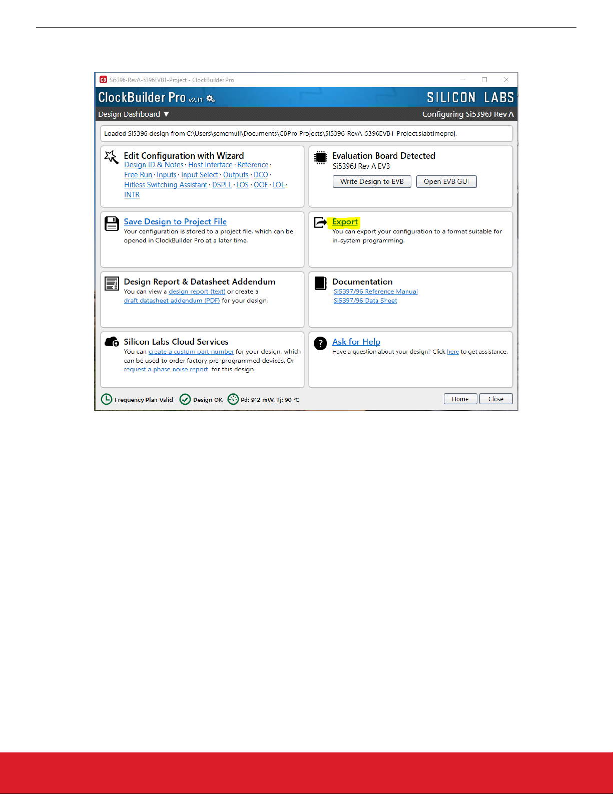
10.5 Workflow Scenario #2: Modifying the Default Silicon Labs-Created Device Configuration
To modify the “default” configuration using the CBPro Wizard, click on Edit Configuration with Wizard:
Using the Si5396J-A-EVB
Figure 10.13. Edit Configuration with Wizard
You will now be taken to the Wizard’s step-by-step menus to allow you to change any of the default plan’s operating configurations.
silabs.com | Building a more connected world. Rev. 1.1 | 21
Page 22

UG336: Si5396J Evaluation Board User's Guide
Using the Si5396J-A-EVB
Figure 10.14. Design Wizard
Note you can click on the icon on the lower left hand corner of the menu to confirm if your frequency plan is valid. After making your
desired changes, you can click on Write to EVB to update the DUT to reconfigure your device real-time. The Design Write status window will appear each time you make a change.
Figure 10.15. Writing Design Status
silabs.com | Building a more connected world. Rev. 1.1 | 22
Page 23

UG336: Si5396J Evaluation Board User's Guide
Using the Si5396J-A-EVB
10.6 Workflow Scenario #3: Testing a User-Created Device Configuration
test a previously created user configuration, open the CBPro Wizard by clicking on the icon on your desktop and then selecting
To
Open Design Project File.
Figure 10.16. Open Design Project File
Locate your CBPro design file (*.slabtimeproj or *.sitproj file).design file in the Windows file browser.
silabs.com | Building a more connected world. Rev. 1.1 | 23
Page 24

UG336: Si5396J Evaluation Board User's Guide
Using the Si5396J-A-EVB
Figure 10.17. Browse to Project File
Select Yes when the WRITE DESIGN to EVB popup appears:
silabs.com | Building a more connected world. Rev. 1.1 | 24
Page 25

UG336: Si5396J Evaluation Board User's Guide
Using the Si5396J-A-EVB
Figure 10.18. Write Design to EVB Dialog
The progress bar will be launched. Once the new design project file has been written to the device, verify the presence and frequencies
of your output clocks and other operating configurations using external instrumentation.
silabs.com | Building a more connected world. Rev. 1.1 | 25
Page 26
UG336: Si5396J Evaluation Board User's Guide
Using the Si5396J-A-EVB
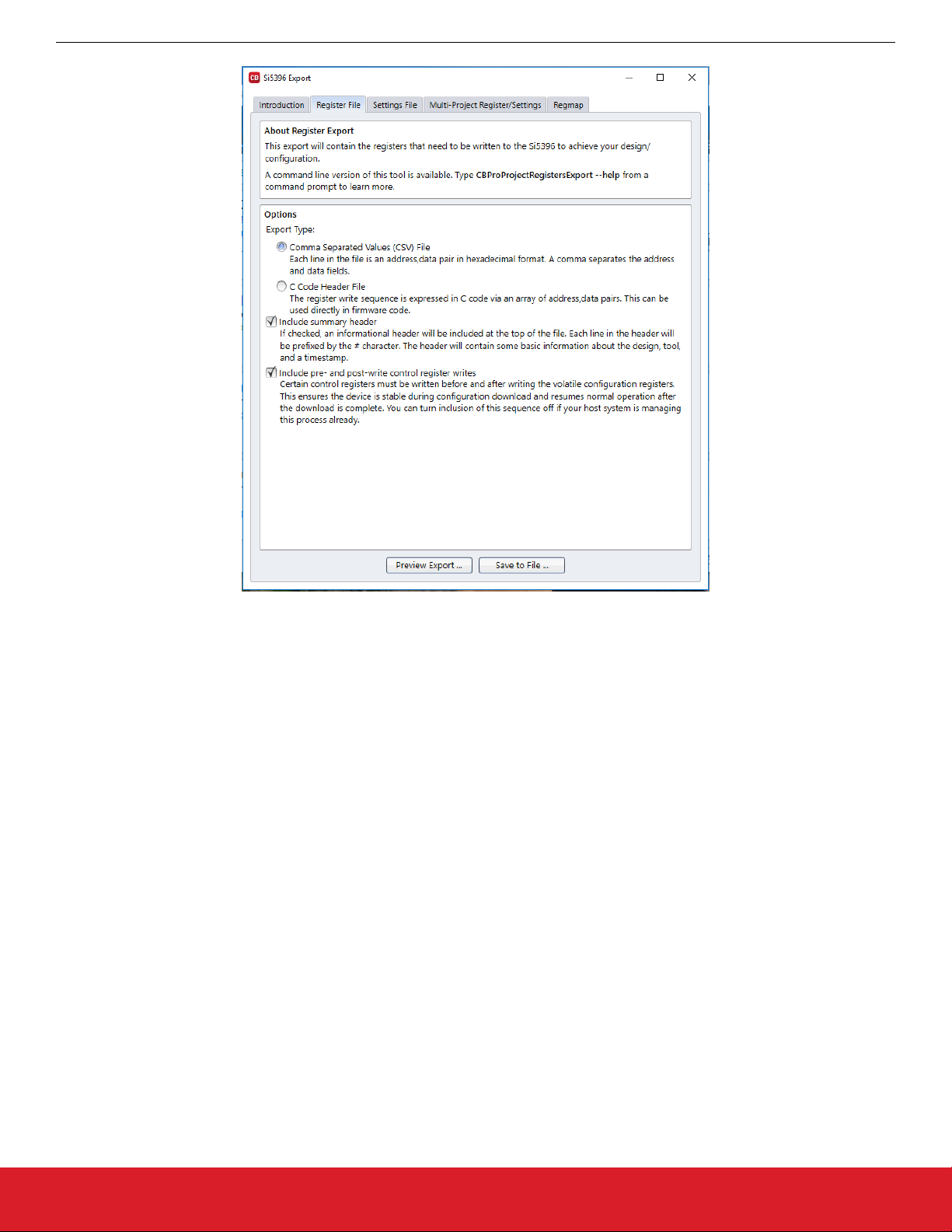
10.7 Exporting the Register Map File for Device Programming by a Host Processor
You can also export your configuration to a file format suitable for in-system programming by selecting Export as shown below:
Figure 10.19. Export Register Map File
You can now write your device’s complete configuration to file formats suitable for in-system programming.
silabs.com | Building a more connected world. Rev. 1.1 | 26
Page 27
UG336: Si5396J Evaluation Board User's Guide
Using the Si5396J-A-EVB
Figure 10.20. Export Settings
silabs.com | Building a more connected world. Rev. 1.1 | 27
Page 28

UG336: Si5396J Evaluation Board User's Guide
Writing a New Frequency Plan or Device Configuration to Non-Volatile Memory (OTP)
11. Writing a New Frequency Plan or Device Configuration to Non-Volatile Memory (OTP)
Note: Writing to the device non-volatile memory (OTP) is NOT the same as writing a configuration into the Si5396 using ClockBuilder
Pro on the Si5396J-A-EVB. Writing a configuration into the EVB from ClockBuilder Pro is done using Si5396 RAM space and can be
done virtually unlimited numbers of times. Writing to OTP is limited as described below.
Refer to the Si5397/96 Reference Manuals and device data sheets for information on how to write a configuration to the EVB DUT’s
non-volatile memory (OTP). The OTP can be programmed a maximum of two times only. Care must be taken to ensure the configuration desired is valid when choosing to write to OTP.
silabs.com | Building a more connected world. Rev. 1.1 | 28
Page 29
UG336: Si5396J Evaluation Board User's Guide
Serial Device Communications
12. Serial Device Communications
12.1 Onboard SPI Support
The MCU onboard the Si5396J-A- EVB communicates with the Si5396 device through a 4-wire SPI (Serial Peripheral Interface) link.
The MCU is the SPI master and the Si5396 device is the SPI slave. The Si5396 device can also support a 2-wire I2C serial interface,
although the Si5396 EVB does NOT support the I2C mode of operation. SPI mode was chosen for the EVB because of the relatively
higher speed transfers supported by SPI vs. I2C.
12.2 External I2C Support
I2C can be supported if driven from an external I2C controller. The serial interface signals between the MCU and Si5396 pass through
shunts loaded on header J17. These jumper shunts must be installed in J17 for normal EVB operation using SPI with CBPro. If testing
of I2C operation via external controller is desired, the shunts in J17 can be removed thereby isolating the on-board MCU from the
Si5396 device. The shunt at JP1 (I2C_SEL) must also be removed to select I2C as Si5396 interface type. An external I2C controller
connected to the Si5396 side of J17 can then communicate to the Si5396 device. (For more information on I2C signal protocol, please
refer to the Si5396 data sheet.)
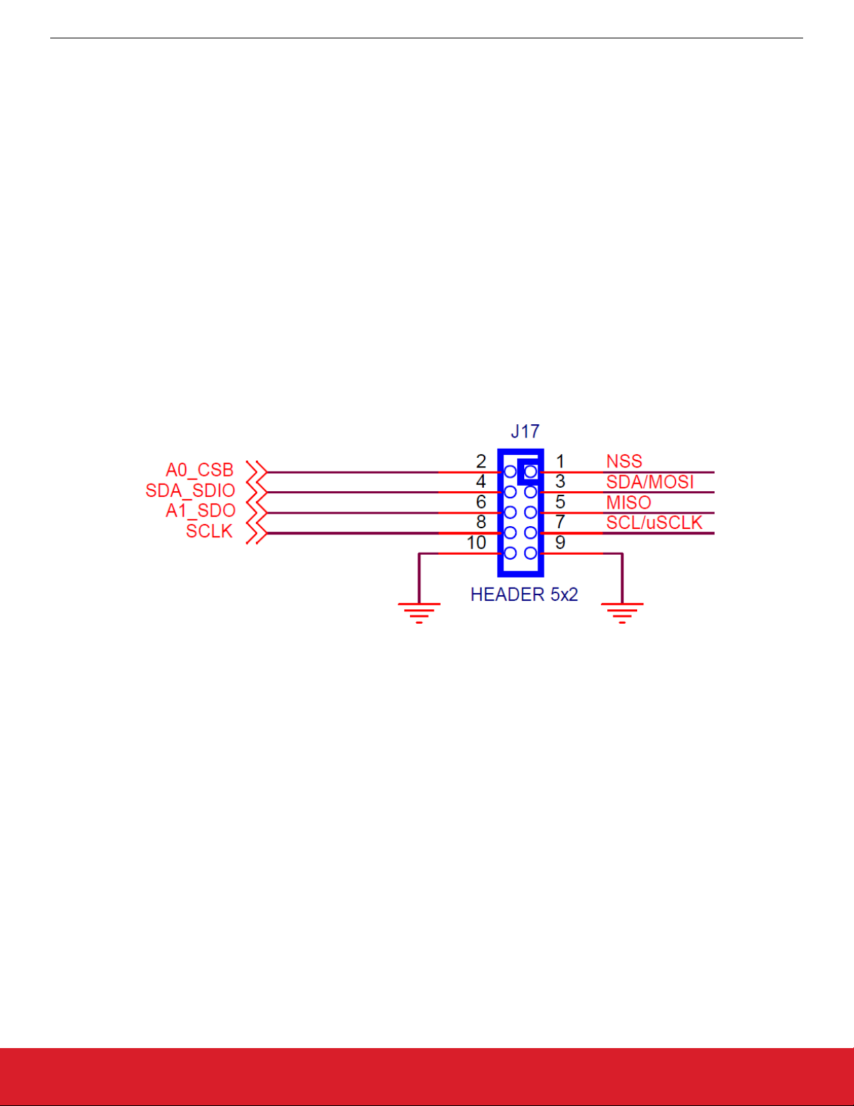
The figure below illustrates the J17 header schematic. J17 even numbered pins (2, 4, 6, etc.) connect to the Si5396 device and the odd
numbered pins (1, 3, 5, etc.) connect to the MCU. Once the jumper shunts have been removed from J17 and JP1, I2C operation should
use J17 pin 4 (DUT_SDA_SDIO) as the I2C SDA and J17 pin 8 (DUT_SCLK) as the I2C SCLK. Please note the external I2C controller
will need to supply its own I2C signal pull-up resistors.
Figure 12.1. Serial Communications Header J17
silabs.com | Building a more connected world. Rev. 1.1 | 29
Page 30
UG336: Si5396J Evaluation Board User's Guide
Si5396J-A-EVB Schematic and Bill of Materials (BOM)
13. Si5396J-A-EVB Schematic and Bill of Materials (BOM)
The Si5396J-A-EVB Schematic and Bill of Materials (BOM) can be found at www.silabs.com/documents/public/schematic-files/si539x-
design-files.zip
Note: Please be aware that the Si5396J-A-EVB schematic is in OrCad Capture hierarchical format and not in a typical “flat” schematic
format.
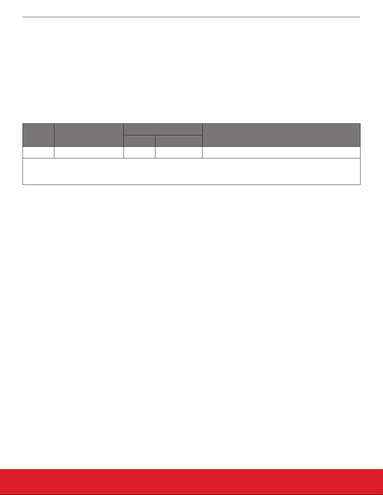
This document supports the evaluation board silkscreened Si5396J-A-EB for the following configurations as described in the table below. The data sheet documents the different Si5396 grades.
Table 13.1. Evaluation Board Configurations
Config # Eval Board Label Si5396 Notes
Grade Revision
1 Si5396J-A-EB J A No Crystal and related components installed.
Note:
1.
The Si5396J-A-EB should be used to evaluate Si5396J/K/L/M plans.
silabs.com | Building a more connected world. Rev. 1.1 | 30
Page 31

14. Revision History
Revision 1.1
November, 2020
•
Changed the front page description to specify 4 output 44-pin Si5396 device
UG336: Si5396J Evaluation Board User's Guide
Revision History
silabs.com | Building a more connected world. Rev. 1.1 | 31
Page 32

ClockBuilder Pro
One-click access to Timing tools,
documentation, software, source
code libraries & more. Available for
Windows and iOS (CBGo only).
www.silabs.com/CBPro
Timing Portfolio
www.silabs.com/timing
Disclaimer
Silicon Labs intends to provide customers with the latest, accurate, and in-depth documentation of all peripherals and modules available for system and software implementers using or
intending to use the Silicon Labs products. Characterization data, available modules and peripherals, memory sizes and memory addresses refer to each specific device, and "Typical"
parameters provided can and do vary in different applications. Application examples described herein are for illustrative purposes only . Silicon Labs reserves the right to make changes without
further notice to the product information, specifications, and descriptions herein, and does not give warranties as to the accuracy or completeness of the included information. Without prior
notification, Silicon Labs may update product firmware during the manufacturing process for security or reliability reasons. Such changes will not alter the specifications or the performance
of the product. Silicon Labs shall have no liability for the consequences of use of the information supplied in this document. This document does not imply or expressly grant any license
to design or fabricate any integrated circuits. The products are not designed or authorized to be used within any FDA Class III devices, applications for which FDA premarket approval is
required, or Life Support Systems without the specific written consent of Silicon Labs. A "Life Support System" is any product or system intended to support or sustain life and/or health,
which, if it fails, can be reasonably expected to result in significant personal injury or death. Silicon Labs products are not designed or authorized for military applications. Silicon Labs
products shall under no circumstances be used in weapons of mass destruction including (but not limited to) nuclear, biological or chemical weapons, or missiles capable of delivering
such weapons. Silicon Labs disclaims all express and implied warranties and shall not be responsible or liable for any injuries or damages related to use of a Silicon Labs product in such
unauthorized applications.
Trademark Information
Silicon Laboratories Inc.®, Silicon Laboratories®, Silicon Labs®, SiLabs® and the Silicon Labs logo®, Bluegiga®, Bluegiga Logo®, ClockBuilder®, CMEMS®, DSPLL®, EFM®, EFM32®,
EFR, Ember®, Energy Micro, Energy Micro logo and combinations thereof, "the world’s most energy friendly microcontrollers", Ember®, EZLink®, EZRadio®, EZRadioPRO®, Gecko®,
Gecko OS, Gecko OS Studio, ISOmodem®, Precision32®, ProSLIC®, Simplicity Studio®, SiPHY®, Telegesis, the Telegesis Logo®, USBXpress® , Zentri, the Zentri logo and Zentri DMS, ZWave®, and others are trademarks or registered trademarks of Silicon Labs. ARM, CORTEX, Cortex-M3 and THUMB are trademarks or registered trademarks of ARM Holdings. Keil is a
registered trademark of ARM Limited. Wi-Fi is a registered trademark of the Wi-Fi Alliance. All other products or brand names mentioned herein are trademarks of their respective holders.
Silicon Laboratories Inc.
400 West Cesar Chavez
Austin, TX 78701
USA
SW/HW
www.silabs.com/CBPro
Quality
www.silabs.com/quality
Support and Community
community.silabs.com
http://www.silabs.com
 Loading...