

Page 1
UG298: Si5xxUC-EVB
Universal Oscillator Evaluation Board
This document describes operation of the Silicon Laboratories Si5xxUC-EVB evaluation
board designed to evaluate any of Silicon Labs’ pin-controlled or I2C configurable Si5xx
XOs or VCXOs. Three device sites are available to support one of either 5mm x 7mm,
3.2mm x 5mm, or 2.5mm x 3.2mm devices in either 4, 6, or 8 pin configurations. Selector switches make it easy to configure device control pins (pins 1, 2, 7, or 8) for proper
operation without the use of jumpers. Similarly, XO device VDD voltage (3.3V, 2.5V,
1.8V) can be selected via switches based on either external +5V (for stand-alone operation) or micro USB sourced +5V USB operation. The EVB also features flexible output
termination circuits and PCB layout optimized for superior signal integrity.
Ext +5V
micro
USB
+VDD
GND
SDA
Vc_In
Power
Select
Switch
Silicon Labs
MCU
Pin 1
Signal
Selector
Switch
I2C Bus
Pin 1
SDA
SCL
Pin 1
Pin 2
Pin 7
Pin 8
Power
Supply
+VDD
XO
Location 1
(5mm x 7mm)
KEY FEATURES
• Evaluation of any Silicon Labs XO or
VCXO (Si51x, Si53x, Si54x, Si55x, Si56x,
Si57x, Si59x)
• AC coupled differential/single-ended output
clocks.
• Voltage control (Vc) port for VCXO
evalution.
• Switch selectable settings. No jumpers.
• External power or USB powered.
• Use stand-alone or with our Pro-
grammable Oscillator Calculator SW tool
Voltage
Selector
Switches
Output
Termination
CLK1_P
CLK1_N
+VDD
GND
SCL
+VDD
GND
SDA
+VDD
GND
SCL
silabs.com | Building a more connected world. Rev. 0.5
Pin 2
Signal
Selector
Switch
Pin 7
Signal
Selector
Switch
Pin 8
Signal
Selector
Switch
Pin 2
Pin 7
Pin 8
Pin 1
Pin 2
Pin 7
Pin 8
Pin 1
Pin 2
Pin 7
Pin 8
XO
Location 2
(3.2mm x 5mm)
XO
Location 3
(2.5mm x 3.2mm)
Output
Termination
Output
Termination
CLK2_P
CLK2_N
CLK3_P
CLK3_N
Page 2

Table of Contents
1. Quick Start - Board Configuration Check List ...................3
2. Functional Description............................4
3. General Operational Restrictions ........................5
3.1 Evaluate Only a Single Device at a Time .....................5
4. Power Supply and I2C Bus Control .......................6
5. Control Signal Switch Settings.........................7
5.1 Oscillator Pin 1 Control DIP Switch (Pin_1_Ctrl) ...................8
5.2 Oscillator Pin 2 Control DIP Switch (Pin_2_Ctrl) ...................9
5.3 Oscillator Pin 7 Control DIP Switch (Pin_7_Ctrl) ...................10
5.4 Oscillator Pin 8 Control DIP Switch (Pin_8_Ctrl) ...................11
6. Supported Devices - Stand-Alone Mode ....................12
7. Supported Devices - Software Controlled Mode - I2C ...............15
8. USB Port and External Powering .......................16
9. Output Clock Terminations .........................17
10. EVB Test Points and LEDs .........................18
10.1 Test Points ...............................18
10.2 LEDs .................................18
11. VCXO Voltage Control Input Circuit .....................19
12. Programmable Oscillator Calculator Tool ...................20
13. Layout of Board .............................21
13.1 Si56x XO and VCXO 2.5x3.2mm Footprint Recommendation ..............22
14. Si5xxUC-EVB Schematic .........................23
silabs.com
| Building a more connected world. Rev. 0.5 | 2
Page 3

UG298: Si5xxUC-EVB
Quick Start - Board Configuration Check List
1. Quick Start - Board Configuration Check List
Mount your oscillator device on the board at appropriate oscillator site location (U1, U2, or U3, but on only one location) if a device is
not yet mounted.
1. Start with EVB board powered down/off.
2. Set DIP switches (described in Section 5. Control Signal Switch Settings) for your specific device:
a. Look up your device as appropriate in the tables of Sections 6. Supported Devices - Stand-Alone Mode or 7. Supported Devi-
ces - Software Controlled Mode - I2C.
b. Make DIP switch settings per table entry for pins 1,2,7,8 as appropriate. See Sections 6. Supported Devices - Stand-Alone
Mode or 7. Supported Devices - Software Controlled Mode - I2C .
3. Verify output termination is appropriate for your device (see Section 9. Output Clock Terminations for more info).
4. Set +5V Select switch (SW5) based on how you will power the EVB, either via USB or via external +5V supply.
5. Connect power, either via USB port or external +5V power supply as chosen in previous step.
6. Output Clocks:
• For pin controlled oscillators, clock output should be available on output SMAs of DUT site in use.
• For I2C oscillators, run appropriate configuration software (e.g., Programmable Oscillator Software tool) and perform device
configuration to get desired output clock.
silabs.com | Building a more connected world. Rev. 0.5 | 3
Page 4

UG298: Si5xxUC-EVB
Functional Description
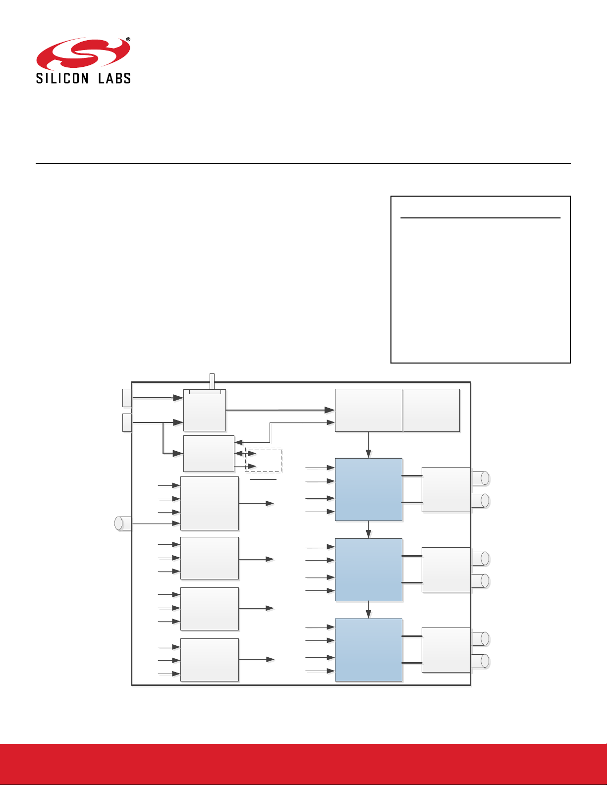
2. Functional Description
The Si5xxUC-EVB is an evaluation board designed to support any Silicon Labs XO/VCXO device. The Si5xxUC-EVB is designed to
operate in one of two general operational modes:
• Stand-alone mode: The stand-alone mode is for evaluation of fixed output frequency or pin-controlled XO/VCXO devices
where I2C support is NOT required to operate or evaluate the device. Control of device pins, such as OE or FS, is done via on-board
switches. In Stand-alone mode the on-board switches must be set according to the requirements of the device installed on the
board. For example, if the installed device is a dual frequency part with output enable, the appropriate switches must be set to assert
output enable (OE) and the frequency select pin (FS) to give the desired output frequency. Device VDD voltage can be set via on-
board switches as well. Switch setting details for Stand-alone mode are shown in Section 4. Power Supply and I2C Bus Control (for
power supply) and Section 5. Control Signal Switch Settings (for device pins).
• Software controlled mode: The software controlled mode is for use with PC-based software tools (such as our Programmable Os-
cillator Calculator Tool) to control/configure the device being evaluated via the device I2C bus. The software controlled mode is pri-
marily intended for I2C controlled XO/VCXO devices. When using software controlled mode, some of the on-board switches must
be placed in specific default settings to allow the on-board MCU to perform I2C control. Other switches must still be used on certain
device signals, like output enable (OE). Switch setting details for software controlled mode are shown in Section 4. Power Supply
and I2C Bus Control (for power supply & I2C) and Section 5. Control Signal Switch Settings (for device pins).
For each of the 3 device locations on the Si5XXUC-EVB, separate sets of SMA outputs and terminations are provided per XO “Device
Under Test” (DUT) location even though only one device may be populated and used at a time (see Section 3. General Operational
Restrictions below). Separate outputs and terminations per device site provides the best possible clock signal integrity for each DUT
location.
silabs.com | Building a more connected world. Rev. 0.5 | 4
Page 5

UG298: Si5xxUC-EVB
General Operational Restrictions
3. General Operational Restrictions
3.1 Evaluate Only a Single Device at a Time
Note: It is strongly recommended to populate only one device on the Si5xxUC-EVB board at a time. Carefully read the next paragraph
for important information.
The Si5xxUC-EVB supports evaluation of a single device in one of three different DUT locations. Device sizes supported are 5mm x
7mm, 3.2mm x 5mm, or 2.5mm x 3.2mm. All device locations can support 4, 6, or 8 pin configurations, but only one device at a time
should be installed in any one of the three locations on the Si5xxUC-EVB. This restriction is made to ensure no problems will occur due
to potential signal crosstalk, power supply over-loading/coupling, or signal contention/loading between multiple devices. Do not simply
remove power from a mounted device in an attempt to place it in an “unused”, but still mounted, state. Board control signals are wired in
parallel to all 3 locations and a non-powered device may load control signals to a powered device under test. Please follow this “one
device at a time” recommendation and only populate one device at a time.
silabs.com | Building a more connected world. Rev. 0.5 | 5
Page 6
UG298: Si5xxUC-EVB
Power Supply and I2C Bus Control
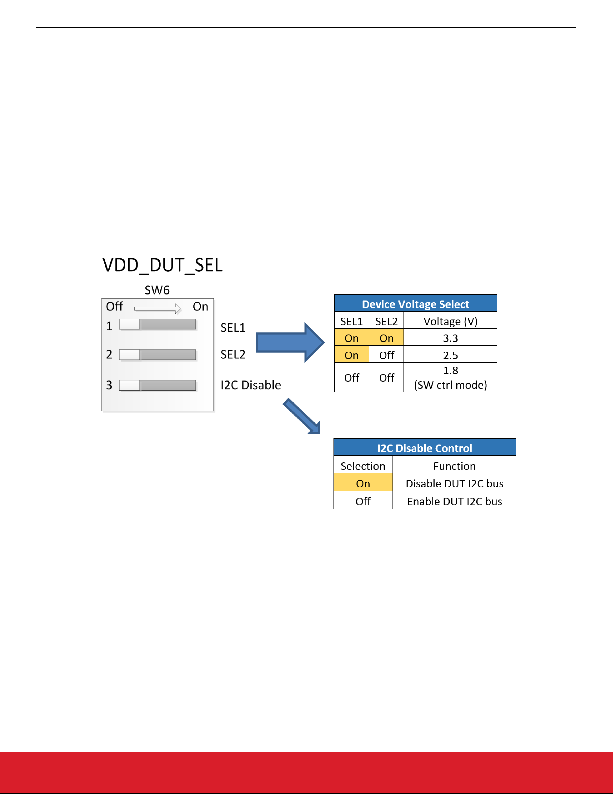
4. Power Supply and I2C Bus Control
The power supply uses a linear voltage regulator to drop the +5 V input supply voltage to one of the supported nominal VDD voltages of
+3.3 V, +2.5 V, or +1.8 V. A switch is provided on the EVB (SW5) to select the +5 V source for the voltage regulator as either the USB
port +5V or an external +5 V source. The EVB power supply supports operation in one of 2 general modes that correspond to the two
operational EVB use cases.
• Stand-alone mode: Power can be sourced from either external supply or USB port, but software is not required and no EVB software
tool should be actively connected to Si5XXUC-EVB when being used in Stand-alone mode. In Stand-alone mode the oscillator device VDD voltage is set via the “VDD_DUT_SEL” switch according to the voltage select table shown below. By default this switch is
set to 1.8 V and will need to be changed if evaluating a non-I2C oscillator with 2.5 V or 3.3 V VDD.
• Software controlled mode: Power can be sourced from either external power supply or USB port, but the Programmable Oscillator
Software tool can be used to set the VDD voltage to the oscillator. In software controlled mode, “VDD_DUT_SEL” switches should
remain set to 1.8 V setting regardless of the desired VDD voltage.
The I2C Disable switch is typically set to the “Off” setting (to enable the on-board MCU to drive the I2C bus) unless the user is attempting to connect an external I2C master to communicate with the oscillator device. The I2C Disable control allows for disabling the onboard I2C buffer to disconnect the oscillator from the on-board MCU. This disconnection is useful if the user wishes to connect an external I2C bus master to communicate with the DUT.
silabs.com | Building a more connected world. Rev. 0.5 | 6
Page 7
UG298: Si5xxUC-EVB
Control Signal Switch Settings
5. Control Signal Switch Settings
Four of the 5 on-board DIP switches (SW1, 2, 3, 4) are used for configuration of the EVB oscillator locations to match any standard
oscillator pin-out. Using this DIP switch arrangement, the Si5xxUC-EVB can be configured to support all Silicon Labs oscillator devices.
The oscillator device pins that can vary in function, depending on the device variant, are pins 1, 2, 7, and 8 as shown in the Device Pinout Mapping table below. Pins 3, 4, 5, and 6 are typically fixed function pins that do not change with device variant.
Note: All device locations on the Si5xxUC-EVB can support up to 8 pin variant devices. Devices with fewer pins (4, 6 pin) can be installed in the same location and will fit within the 8 pin footprint.
Device Pin-out Mapping
4 pin
Device
6 pin
Device
8 pin
Device
DIP Switch
Function
Options
1 1 1 Pin_1_Ctrl (SW1) FS/OE/SDA/Vc
- 2 2 Pin_2_Ctrl (SW2) FS/OE/SCL
2 3 3 - GND
3 4 4 - Output
- 5 5 - Output
4 6 6 - VDD
1
1
1
1
- - 7 Pin_7_Ctrl (SW3) FS/SDA
- - 8 Pin_8_Ctrl (SW4) FS/SCL
Note:
1. Fixed function pins
Configuration details of each of the 4 variable pin function DIP switches is described in following sections. For devices that may not
utilize all 4 of the variable pin function switches, the corresponding unused DIP switch can be set to the NC setting (all Off position).
Make sure to make the following switch settings with the Si5xxUC-EVB powered down. Once all are set appropriately, the board may
be powered on.
silabs.com | Building a more connected world. Rev. 0.5 | 7
Page 8
UG298: Si5xxUC-EVB
Control Signal Switch Settings
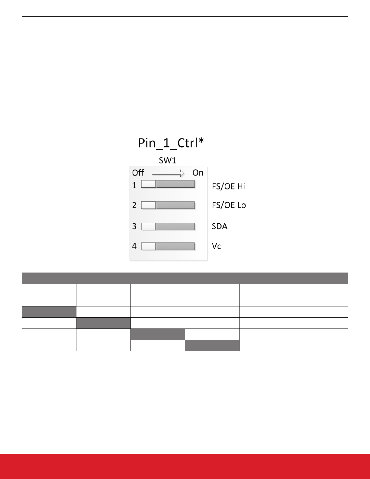
5.1 Oscillator Pin 1 Control DIP Switch (Pin_1_Ctrl)
The pin 1 control DIP switch allows oscillator pin 1 to be driven from any of these 4 sources.
1. High (VDD) level
2. Low (GND) level
3. I2C bus SDA signal
4. External control voltage Vc (for VCXO applications)
Note: The 4 signal sources listed above are connected on separate pins on left side of the switch and all pins on right side are tied
together (common) and then connect to pin 1 of the oscillator. This means that only one (1) of the switches in this DIP switch bank
can be in the ON position at a time. Switching more than 1 switch to the on position at a time may cause undesired behavior. All
switches can be set to OFF position to effectively isolate pin 1 from any signal source and is the No Connect (NC) state.
To determine the required Pin 1 switch settings for your specific device, please refer to the Supported Device Tables in Chapter
6. Supported Devices - Stand-Alone Mode and Chapter 7. Supported Devices - Software Controlled Mode - I2C.
Pin 1 DIP Switch (4, 6, or 8 pin DUT)
1 2 3 4 Pin 1 Signal
Off Off Off Off NC
On Off Off Off FS/OE high
Off On Off Off FS/OE low
Off Off On Off SDA
Off Off Off On Vc
silabs.com | Building a more connected world. Rev. 0.5 | 8
Page 9

UG298: Si5xxUC-EVB
Control Signal Switch Settings
5.2 Oscillator Pin 2 Control DIP Switch (Pin_2_Ctrl)
This DIP switch allows oscillator pin 2 to be driven from 1 of 3 sources.
1. High (VDD) level
2. Low (GND) level
3. I2C bus SCL signal
Note: The 3 signal sources listed above are located on separate pins on the left side of the switch and all pins on the right side are tied
together (common) and then connect to pin 2 of the oscillator. This means that only one (1) of the switches in this DIP switch bank
can be in the ON position at a time. Switching more than 1 switch to the ON position at a time may cause undesired behavior. All
switches set to OFF position effectively isolates pin 2 from any signal source and is the No Connect (NC) state.
To determine the required Pin 2 switch settings for your specific device, please refer to the Supported Device Tables in Chapter
6. Supported Devices - Stand-Alone Mode and Chapter 7. Supported Devices - Software Controlled Mode - I2C.
Pin 2 DIP Switch (6 or 8 pin DUT)
1 2 3 Pin 2 Signal
Off Off Off NC
On Off Off FS/OE high
Off On Off FS/OE low
Off Off On SCL
silabs.com | Building a more connected world. Rev. 0.5 | 9
Page 10

UG298: Si5xxUC-EVB
Control Signal Switch Settings
5.3 Oscillator Pin 7 Control DIP Switch (Pin_7_Ctrl)
This DIP switch allows oscillator pin 7 to be driven from 1 of 3 sources.
1. High (VDD) level
2. Low (GND) level
3. I2C bus SDA signal
Note: The 3 signal sources listed above are located on separate pins on the left side of the switch and all pins on the right side are tied
together (common) and then connect to pin 7 of the oscillator. This means that only one (1) of the switches in this DIP switch bank
can be in the ON position at a time. Switching more than 1 switch to the ON position at a time may cause undesired behavior. All
switches set to OFF position effectively isolates pin 7 from any signal source and is the No Connect (NC) state.
To determine the required Pin 7 switch settings for your specific device, please refer to the Supported Device Tables in Chapter
6. Supported Devices - Stand-Alone Mode and Chapter 7. Supported Devices - Software Controlled Mode - I2C.
Pin 7 DIP Switch (8 pin DUT)
1 2 3 Pin 7 Signal
Off Off Off NC
On Off Off FS high
Off On Off FS low
Off Off On SDA
silabs.com | Building a more connected world. Rev. 0.5 | 10
Page 11

UG298: Si5xxUC-EVB
Control Signal Switch Settings
5.4 Oscillator Pin 8 Control DIP Switch (Pin_8_Ctrl)
This DIP switch allows oscillator pin 8 to be driven from 1 of 3 sources.
1. High (VDD) level
2. Low (GND) level
3. I2C bus SCL signal
Note: The 3 signal sources listed above are located on separate pins on the left side of the switch and all pins on the right side are tied
together (common) and then connect to pin 8 of the oscillator. This means that only one (1) of the switches in this DIP switch bank
can be in the ON position at a time. Switching more than 1 switch to the ON position at a time may cause undesired behavior. All
switches set to OFF position effectively isolates pin 8 from any signal source and is the No Connect (NC) state.
To determine the required Pin 8 switch settings for your specific device, please refer to the Supported Device Tables in Chapter
6. Supported Devices - Stand-Alone Mode and Chapter 7. Supported Devices - Software Controlled Mode - I2C.
Pin 8 DIP Switch (8 pin DUT)
1 2 3 Pin 8 Signal
Off Off Off NC
On Off Off FS high
Off On Off FS low
Off Off On SCL
silabs.com | Building a more connected world. Rev. 0.5 | 11
Page 12

UG298: Si5xxUC-EVB
Supported Devices - Stand-Alone Mode
6. Supported Devices - Stand-Alone Mode
If using the Si5XXUC-EVB with a device that is either fixed frequency or has pin-controlled output frequency, this “Stand-alone mode”
section should be used to configure the EVB.
If you have a device installed that utilizes the I2C bus for making frequency or other changes to the device, please refer to Section
7. Supported Devices - Software Controlled Mode - I2C.
The tables below show pin controlled XO and VCXO devices supported by the Si5xxUC-EVB along with possible package sizes and
control pin mapping. The control pin mapping can be used to determine the corresponding switch settings on the Si5xxUC-EVB.
Table 6.1. Pin Controlled XOs
SiLabs
Device
Si510 XO Single
Si510 XO Single (Diff) 6 5x7, 3.2x5,
Type # Freqs # Pins Pkg Sizes
(mm x mm)
4 5x7, 3.2x5,
(CMOS)
2.5x3.2
Pin 1
Control
OE - - -
Pin 2
Control
Pin 7
Control
Pin 8
Control
Pin 4 Output
1
CLK
Pin 5 Output
-
NC OE - - CLK+ CLK-
2.5x3.2
Si511 XO Single 6 5x7, 3.2x5,
OE NC - - CLK+ CLK-
2.5x3.2
Si512 XO Dual
(CMOS)
Si512 XO Dual (Diff) 6 5x7, 3.2x5,
6 5x7, 3.2x5,
2.5x3.2
FS OE - - CLK NC
FS OE - - CLK+ CLK-
2.5x3.2
Si513 XO Dual
(CMOS)
Si513 XO Dual (Diff) 6 5x7, 3.2x5,
6 5x7, 3.2x5,
2.5x3.2
OE FS - - CLK NC
OE FS - - CLK+ CLK-
2.5x3.2
Si530 XO Single (Diff) 6 5x7 NC OE - - CLK+ CLK-
Si530 XO Single
6 5x7 OE NC - - CLK NC
(CMOS)
Si531 XO Single 6 5x7 OE NC - - CLK+ CLK-
Si532 XO Dual (Diff) 6 5x7 FS OE - - CLK+ CLK-
Si532 XO Dual
6 5x7 FS OE - - CLK NC
(CMOS)
Si533 XO Dual (Diff) 6 5x7 OE FS - - CLK+ CLK-
Si533 XO Dual
6 5x7 OE FS - - CLK NC
(CMOS)
Si534 XO Quad (Diff) 8 5x7 NC OE FS1 FS0 CLK+ CLK-
Si534 XO Quad
8 5x7 NC OE FS1 FS0 CLK NC
(CMOS)
Si535 XO Single 6 5x7 NC OE - - CLK+ CLK-
Si536 XO Single 6 5x7 OE NC - - CLK+ CLK-
Si540 XO Single 6 5x7, 3.2x5,
OE/NC NC/OE - - CLK+ CLK-
2.5x3.2
Si541 XO Dual 6 5x7, 3.2x5,
OE/FS FS/OE - - CLK+ CLK-
2.5x3.2
silabs.com | Building a more connected world. Rev. 0.5 | 12
Page 13

UG298: Si5xxUC-EVB
Supported Devices - Stand-Alone Mode
SiLabs
Device
Type # Freqs # Pins Pkg Sizes
(mm x mm)
Si542 XO Quad 8 5x7, 3.2x5,
2.5x3.2
Si544 XO Single/Dual/
Quad (or
8 5x7, 3.2x5,
2.5x3.2
I2C)
Si545 XO Single 6 5x7, 3.2x5,
2.5x3.2
Si546 XO Dual 6 5x7, 3.2x5,
2.5x3.2
Si547 XO Quad 8 5x7, 3.2x5,
2.5x3.2
Si549 XO Single/Dual/
Quad (or
8 5x7, 3.2x5,
2.5x3.2
I2C)
Si560 XO Single 6 5x7, 3.2x5,
2.5x3.2
Si561 XO Dual 6 5x7, 3.2x5,
2.5x3.2
Si562 XO Quad 8 5x7, 3.2x5,
2.5x3.2
Pin 1
Control
Pin 2
Control
Pin 7
Control
Pin 8
Control
Pin 4 Output
Pin 5 Output
OE/NC NC/OE FS1 FS0 CLK+ CLK-
OE/NC/FS OE/NC/FS SDA/FS1 SCL/FS0 CLK+ CLK-
OE/NC NC/OE - - CLK+ CLK-
OE/FS FS/OE - - CLK+ CLK-
OE/NC NC/OE FS1 FS0 CLK+ CLK-
OE/NC/FS OE/NC/FS SDA/FS1 SCL/FS0 CLK+ CLK-
OE/NC NC/OE - - CLK+ CLK-
OE/FS FS/OE - - CLK+ CLK-
OE/NC NC/OE FS1 FS0 CLK+ CLK-
Si564 XO Single/Dual/
Quad (or
8 5x7, 3.2x5,
2.5x3.2
OE/NC/FS OE/NC/FS SDA/FS1 SCL/FS0 CLK+ CLK-
I2C)
Si590 XO Single (Diff) 6 5x7, 3.2x5 NC OE - - CLK+ CLK-
Si590 XO Single
6 5x7, 3.2x5 OE NC - - CLK NC
(CMOS)
Si591 XO Single 6 5x7, 3.2x5 OE NC - - CLK+ CLK-
Note:
1. The pin number headings in Table 6.1 apply to 6/8 pin parts only. 4-pin devices like the Single CMOS Si510 have the clock output
on pin 3 instead of pin 4. Please see the Si510/511 Data Sheet for more details on the pinout.
silabs.com | Building a more connected world. Rev. 0.5 | 13
Page 14

Table 6.2. Pin Controlled VCXOs
UG298: Si5xxUC-EVB
Supported Devices - Stand-Alone Mode
SiLabs
Device
Si515 VCXO Single
Si515 VCXO Single
Si516 VCXO Dual
Si516 VCXO Dual (Diff) 6 5x7, 3.2x5,
Type # Freqs # Pins Pkg Sizes
(mm x mm)
6 5x7, 3.2x5,
(CMOS)
2.5x3.2
6 5x7, 3.2x5,
(Diff)
2.5x3.2
6 5x7, 3.2x5,
(CMOS)
2.5x3.2
Pin 1
Control
Pin 2
Control
Pin 7
Control
Pin 8
Control
Pin 4 Output
Pin 5 Output
Vc OE - - CLK NC
Vc OE - - CLK+ CLK-
Vc FS - - CLK NC
Vc FS - - CLK+ CLK-
2.5x3.2
Si550 VCXO Single 6 5x7 Vc OE - - CLK+ CLK-
Si552 VCXO Dual 6 5x7 Vc FS - - CLK+ CLK-
Si554 VCXO Quad 8 5x7 Vc OE FS1 FS0 CLK+ CLK-
Si565 VCXO Single 6 5x7, 3.2x5,
Vc OE - - CLK+ CLK-
2.5x3.2
Si566 VCXO Dual 6 5x7, 3.2x5,
Vc FS - - CLK+ CLK-
2.5x3.2
Si567 VCXO Quad 8 5x7, 3.2x5,
Vc OE FS1 FS0 CLK+ CLK-
2.5x3.2
Si569 VCXO Single/
Dual (or
8 5x7, 3.2x5,
2.5x3.2
Vc OE/FS SDA SCL CLK+ CLK-
I2C)
Si595 VCXO Single 6 5x7, 3.2x5 Vc OE - - CLK+ CLK-
Si596 VCXO Dual 6 5x7, 3.2x5 Vc FS - - CLK+ CLK-
Si597 VCXO Quad 8 5x7 Vc OE FS1 FS0 CLK+ CLK-
silabs.com | Building a more connected world. Rev. 0.5 | 14
Page 15

UG298: Si5xxUC-EVB
Supported Devices - Software Controlled Mode - I2C
7. Supported Devices - Software Controlled Mode - I2C
If using the Si5XXUC-EVB with a device that utilizes the I2C bus for making frequency or other changes to the device, this “software
controlled mode” section should be used to configure the EVB.
If you have a device installed that is either fixed frequency or has pin-controlled output frequency, refer to Section 6. Supported Devices
- Stand-Alone Mode.
The tables below show I2C XO and I2C VCXO devices supported by the Si5xxUC-EVB along with possible package sizes and control
pin mapping. The control pin mapping can be used to determine the corresponding switch settings on the Si5xxUC-EVB when using
software controlled mode.
Table 7.1. I2C XOs
SiLabs
Device
Si514 XO I2C 6 5x7, 3.2x5,
Si544 XO
Si549 XO
Si564 XO
Si570 XO
Si598 XO
SiLabs
Device
Si569 VCXO
Type # Freqs # Pins Pkg Sizes
(mm x mm)
2.5x3.2
I2C or (Single/
Dual/Quad)
I2C or (Single/
Dual/Quad)
I2C or (Single/
Dual/Quad)
I2C
I2C
Type # Freqs # Pins Pkg Sizes
I2C or (Single/
Dual)
8 5x7, 3.2x5,
2.5x3.2
8 5x7, 3.2x5,
2.5x3.2
8 5x7, 3.2x5,
2.5x3.2
8 5x7 NC OE SDA SCL CLK+ CLK-
8 5x7 NC OE SDA SCL CLK+ CLK-
(mm x mm)
8 5x7, 3.2x5,
2.5x3.2
Pin 1
Control
SDA SCL - - CLK+ CLK-
OE/NC/FS OE/NC/FS SDA/FS1 SCL/FS0 CLK+ CLK-
OE/NC/FS OE/NC/FS SDA/FS1 SCL/FS0 CLK+ CLK-
OE/NC/FS OE/NC/FS SDA/FS1 SCL/FS0 CLK+ CLK-
Table 7.2. I2C VCXOs
Pin 1
Control
Vc OE/FS SDA SCL CLK+ CLK-
Pin 2
Control
Pin 2
Control
Pin 7
Control
Pin 7
Control
Pin 8
Control
Pin 8
Control
Pin 4 Output
Pin 4 Output
Pin 5 Output
Pin 5 Output
Si571 VCXO
Si599 VCXO
silabs.com | Building a more connected world. Rev. 0.5 | 15
I2C
I2C
8 5x7 Vc OE SDA SCL CLK+ CLK-
8 5x7 Vc OE SDA SCL CLK+ CLK-
Page 16

UG298: Si5xxUC-EVB
USB Port and External Powering
8. USB Port and External Powering
The USB port on the Si5xxUC-EVB utilizes a micro-USB connector that is located on the left edge of the board on the bottom side. A 2meter micro USB cable is provided with the EVB kit. Any micro USB cable can be used that supports full USB connectivity.
If powering the EVB via the USB port, make sure switch SW5 is in the “USB” position. If properly connected to a live USB port, the
green VBUS_5V should illuminate.
If powering the board via an external +5 V power supply, make sure SW5 is in the “EXT” position. Once +5 V is connected to the board
via the +5V_EXT connections, the green +5V_EXT LED should illuminate.
silabs.com | Building a more connected world. Rev. 0.5 | 16
Page 17
UG298: Si5xxUC-EVB
Output Clock Terminations
9. Output Clock Terminations
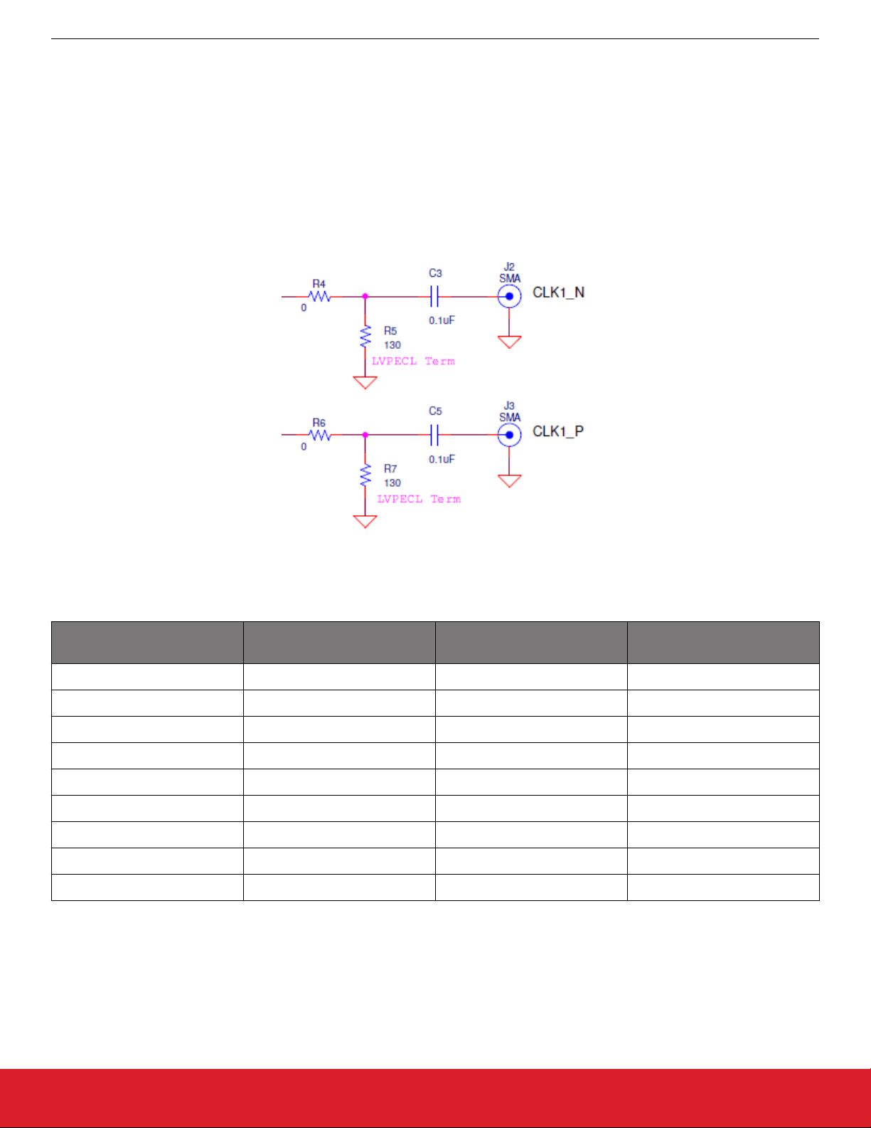
The drawing in the figure below shows the default output termination circuit for CLK1 output of the Si5xxUC-EVB. This default source
termination is for typical 3.3 V LVPECL. CLK2 and CLK3 are also terminated similarly for 3.3 V LVPECL. If not using LVPECL, this
termination circuit may require component modification. The following table gives examples of recommended output termination components for various output formats when using Si51x, Si53x, Si54x, Si55x, Si56x, Si57x, and Si59x devices, but always refer to the spe-
cific device data sheet and/or appropriate application note for details of required output source termination for the specific
device being evaluated.
Note that LVPECL, LVDS, and CML output formats require a 50 Ω termination of each output at the receiver (or 100 Ω differential).
These termination components must be placed as close to the receiver as possible and are therefore not included on the Si5xxUC-EVB
layout.
Figure 9.1. CLK1 Output Default Terminations
Table 9.1. Example Output Clock Source Terminations (Si51x, Si53x, Si54x, Si55x, Si56x, Si57x, and Si59x only)
Output Format Series Resistor Position (e.g.,
R4, R6)
LVPECL 3.3 V: AC coupled 0 Ω 130 Ω 0.1μF
LVPECL 2.5 V: AC coupled 0 Ω 90 Ω 0.1μF
LVPECL: DC coupled 0 Ω Remove replace w/ 0 Ω
LVDS : AC coupled 0 Ω Remove 0.1μF
LVDS : DC coupled 0 Ω Remove replace w/ 0 Ω
HCSL 0 Ω Remove replace w/ 0 Ω
CML 0 Ω Remove 0.1μF
LVCMOS : AC coupled 0 Ω Remove 0.1μF
LVCMOS : DC coupled 0 Ω Remove replace w/ 10 Ω
Parallel Resistor Position
(e.g., R5, R7)
Series Capacitor Position
(e.g., C3, C5)
silabs.com | Building a more connected world. Rev. 0.5 | 17
Page 18

UG298: Si5xxUC-EVB
EVB Test Points and LEDs
10. EVB Test Points and LEDs
10.1 Test Points
The Si5xxUC-EVB has many test points that are useful for probing various nodes and/or making connections to external test equipment. Please refer to the schematic for the functionality of the various test points.
One set of test points in particular provides oscillator current sense capability and is shown in the drawing below. These two test points
allow an external voltage measurement to be taken across the two test points to determine the current being used by the oscillator.
Since the resistor value is 1 Ω, the voltage measured across these 2 test points corresponds to the current through the resistor. For
example, if the measured voltage is 75 mV, the current flow is 75 mA. Each oscillator site has this current sense circuit.
Figure 10.1. Current Sense Test Points
10.2 LEDs
The Si5xxUC-EVB has 5 status LEDs as shown in table below. The board silkscreen identifies each LED.
Table 10.1. Status LEDs
LED name Color Location Description
+5V_EXT Green D1
VBUS_5V Green D5 USB +5 V is present (independent of +5V_SELECT (SW5) switch setting)
VDD_3.3 Green D4 On-board MCU 3.3 V is present
USB_ACT Red D3 USB port activity
Aux Red D2 TBD (spare)
External +5 V source is present (independent of +5V_SELECT (SW5)
switch setting)
silabs.com | Building a more connected world. Rev. 0.5 | 18
Page 19

UG298: Si5xxUC-EVB
VCXO Voltage Control Input Circuit
11. VCXO Voltage Control Input Circuit
The drawing below shows the VCXO control voltage input (VC_IN) circuit used for evaluation of VCXOs. The VCXO control voltage can
be applied using the J1 SMA connector, or using TP3/TP6. A simple RC circuit is included to low-pass filter any noise on the input. The
RC circuit components can be removed or modified as required for your application.
Figure 11.1. VCXO Control Voltage Input "VC_IN"
silabs.com | Building a more connected world. Rev. 0.5 | 19
Page 20

UG298: Si5xxUC-EVB
Programmable Oscillator Calculator Tool
12. Programmable Oscillator Calculator Tool
The Programmable Oscillator Software Tool can be used with the Si5xxUC-EVB. This tool and corresponding Programmable Oscillator
Software Tool User's Guide can be found on the Oscillator Software Tools page.
silabs.com | Building a more connected world. Rev. 0.5 | 20
Page 21

13. Layout of Board
UG298: Si5xxUC-EVB
Layout of Board
silabs.com | Building a more connected world. Rev. 0.5 | 21
Page 22

UG298: Si5xxUC-EVB
Layout of Board
13.1 Si56x XO and VCXO 2.5x3.2mm Footprint Recommendation
For optimal thermal relief, use two ground vias next to the GND pin of the oscillator. Each via should have a 50mm diameter with a
25mm drill. These vias should be directly connected to the board's internal ground layers without the use of thermal relief spokes. This
two via design has been implemented in all Si5xxUC-EVBs REV 4.0 or greater.
Figure 13.1. Si56x 2.5x3.2mm Footprint
silabs.com | Building a more connected world. Rev. 0.5 | 22
Page 23

14. Si5xxUC-EVB Schematic
UG298: Si5xxUC-EVB
Si5xxUC-EVB Schematic
silabs.com | Building a more connected world. Rev. 0.5 | 23
Page 24

UG298: Si5xxUC-EVB
Si5xxUC-EVB Schematic
silabs.com | Building a more connected world. Rev. 0.5 | 24
Page 25

ClockBuilder Pro
One-click access to Timing tools,
documentation, software, source
code libraries & more. Available for
Windows and iOS (CBGo only).
www.silabs.com/CBPro
Timing Portfolio
www.silabs.com/timing
Disclaimer
Silicon Labs intends to provide customers with the latest, accurate, and in-depth documentation of all peripherals and modules available for system and software implementers using or
intending to use the Silicon Labs products. Characterization data, available modules and peripherals, memory sizes and memory addresses refer to each specific device, and "Typical"
parameters provided can and do vary in different applications. Application examples described herein are for illustrative purposes only . Silicon Labs reserves the right to make changes without
further notice to the product information, specifications, and descriptions herein, and does not give warranties as to the accuracy or completeness of the included information. Without prior
notification, Silicon Labs may update product firmware during the manufacturing process for security or reliability reasons. Such changes will not alter the specifications or the performance
of the product. Silicon Labs shall have no liability for the consequences of use of the information supplied in this document. This document does not imply or expressly grant any license
to design or fabricate any integrated circuits. The products are not designed or authorized to be used within any FDA Class III devices, applications for which FDA premarket approval is
required, or Life Support Systems without the specific written consent of Silicon Labs. A "Life Support System" is any product or system intended to support or sustain life and/or health,
which, if it fails, can be reasonably expected to result in significant personal injury or death. Silicon Labs products are not designed or authorized for military applications. Silicon Labs
products shall under no circumstances be used in weapons of mass destruction including (but not limited to) nuclear, biological or chemical weapons, or missiles capable of delivering
such weapons. Silicon Labs disclaims all express and implied warranties and shall not be responsible or liable for any injuries or damages related to use of a Silicon Labs product in such
unauthorized applications.
Trademark Information
Silicon Laboratories Inc.®, Silicon Laboratories®, Silicon Labs®, SiLabs® and the Silicon Labs logo®, Bluegiga®, Bluegiga Logo®, ClockBuilder®, CMEMS®, DSPLL®, EFM®, EFM32®,
EFR, Ember®, Energy Micro, Energy Micro logo and combinations thereof, "the world’s most energy friendly microcontrollers", Ember®, EZLink®, EZRadio®, EZRadioPRO®, Gecko®,
Gecko OS, Gecko OS Studio, ISOmodem®, Precision32®, ProSLIC®, Simplicity Studio®, SiPHY®, Telegesis, the Telegesis Logo®, USBXpress® , Zentri, the Zentri logo and Zentri DMS, ZWave®, and others are trademarks or registered trademarks of Silicon Labs. ARM, CORTEX, Cortex-M3 and THUMB are trademarks or registered trademarks of ARM Holdings. Keil is a
registered trademark of ARM Limited. Wi-Fi is a registered trademark of the Wi-Fi Alliance. All other products or brand names mentioned herein are trademarks of their respective holders.
Silicon Laboratories Inc.
400 West Cesar Chavez
Austin, TX 78701
USA
SW/HW
www.silabs.com/CBPro
Quality
www.silabs.com/quality
Support and Community
community.silabs.com
http://www.silabs.com
 Loading...