Silicon Labs Si5396C/L User Manual

UG467: Si5396C/L Evaluation Board
User's Guide
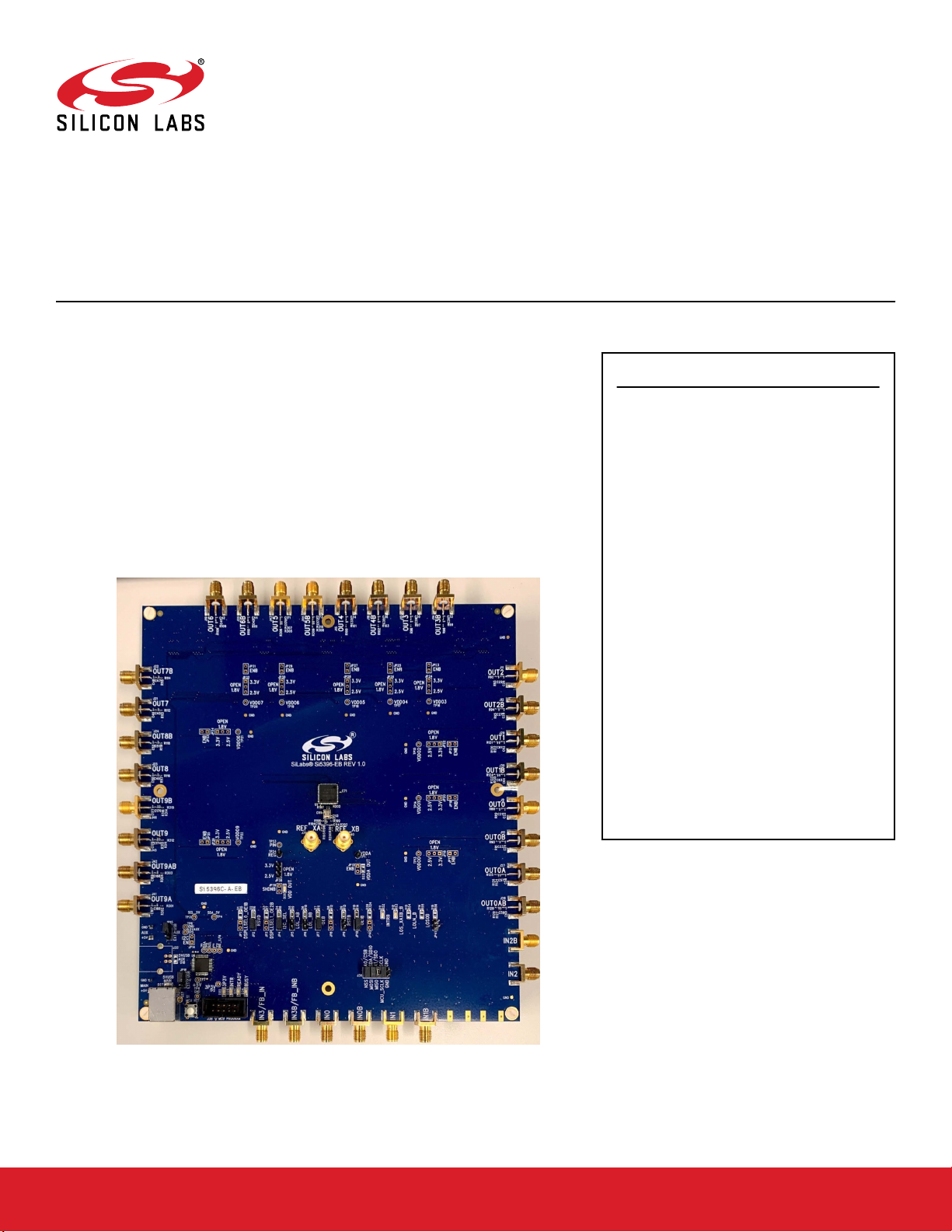
The Si5396C/L -EVB is used for evaluating the Si5396C/L Any-Frequency, Any-Output, Jitter-Attenuating Clock Multiplier. The Grade C board requires an external reference. The Grade L board does not require a reference because it is internal to the
chip. This user guide is intended for both the Si5396C and Si5396L EVBs. The device
grade and revision is distinguished by a white 1 x 0.187 inch label installed in the lower left corner of the board. In the example below, the label, "SI5396C-A-EB", indicates
the evaluation board has been assembled with an Si5396 device, Grade C, Revision
A, installed. (For ordering purposes only, the terms “EB” and “EVB” refer to the board
and the kit respectively. For the purpose of this document, the terms are synonymous
in context.). Note that the Si5396A/B/J/K are all 4-output, 2 PLL devices in a 44-pin
package, while the Si5396C/D/L/M are 12-output devices in a 64-pin package. This
user guide is for the Si5396C/D/L/M grade 12-output, 2 PLL devices.
KEY FEATURES
• Si5396C-A-EVB for evaluating external
reference versions Si5396C/D
• Si5396L-A-EVB for evaluating internal
reference versions Si5396L/M
• Powered from USB port or external power
supply
•
Onboard 48 MHz XTAL or Reference SMA
Inputs allow holdover mode of operation on
the Si5396C
•
ClockBuilder Pro® (CBPro) GUI
programmable VDD supply allows device to
operate from 3.3 V, 2.5 V, or 1.8 V
• CBPro GUI programmable VDDO supplies
allow each of the outputs to have its own
power supply voltage selectable from 3.3 V,
2.5 V, or 1.8 V
• CBPro GUI-controlled voltage, current, and
power measurements of VDD and all VDDO
supplies
• Status LEDs for power supplies and control/
status signals of Si5396C/L
• SMA connectors for input clocks, output
clocks, and optional external timing reference
clock to be used on external reference
grades only
silabs.com | Building a more connected world. Rev. 1.0

Table of Contents
1. Functional Block Diagram ..........................3
Si5396C/L EVB Support Documentation and ClockBuilder Pro Software .........4
2.
3. Quick Start ................................5
4. Jumper Defaults ..............................6
5. Status LEDs................................7
6. External Reference Input (XA/XB)........................8
7. Clock Input Circuits (INx/INxB) .........................9
8. Clock Output Circuits (OUTx/OUTxB) .....................10
9. Installing ClockBuilder Pro Desktop Software ..................11
10. Using the Si5396C/L EVB .........................12
10.1 Connecting the EVB to Your Host PC ......................12
10.2 Additional Power Supplies .........................13
10.3 Overview of ClockBuilder Pro Applications ....................13
10.4 Common ClockBuilder Pro Workflow Scenarios ..................15
10.5 Workflow Scenario 1: Testing a Silicon Labs Default Configuration ............15
10.5.1 Verify Free-Run Mode Operation ......................18
10.5.2 Verify Locked Mode Operation .......................20
10.6 Workflow Scenario 2: Modifying the Default Silicon Labs-Created Device Configuration .....21
10.7 Workflow Scenario 3: Testing a User-Created Device Configuration ...........23
10.8 Exporting the Register Map File for Device Programming by a Host Processor ........25
11. Writing a New Frequency Plan or Device Configuration to Non-Volatile Memory (OTP) ..26
12. Serial Device Communications .......................27
12.1 Onboard SPI Support ...........................27
12.2 External I2C Support ...........................27
13. Si5396C/L EVB Schematic, Layout, and Bill of Materials (BOM) ...........28
silabs.com | Building a more connected world. Rev. 1.0 | 2

UG467: Si5396C/L Evaluation Board User's Guide
Functional Block Diagram
1. Functional Block Diagram
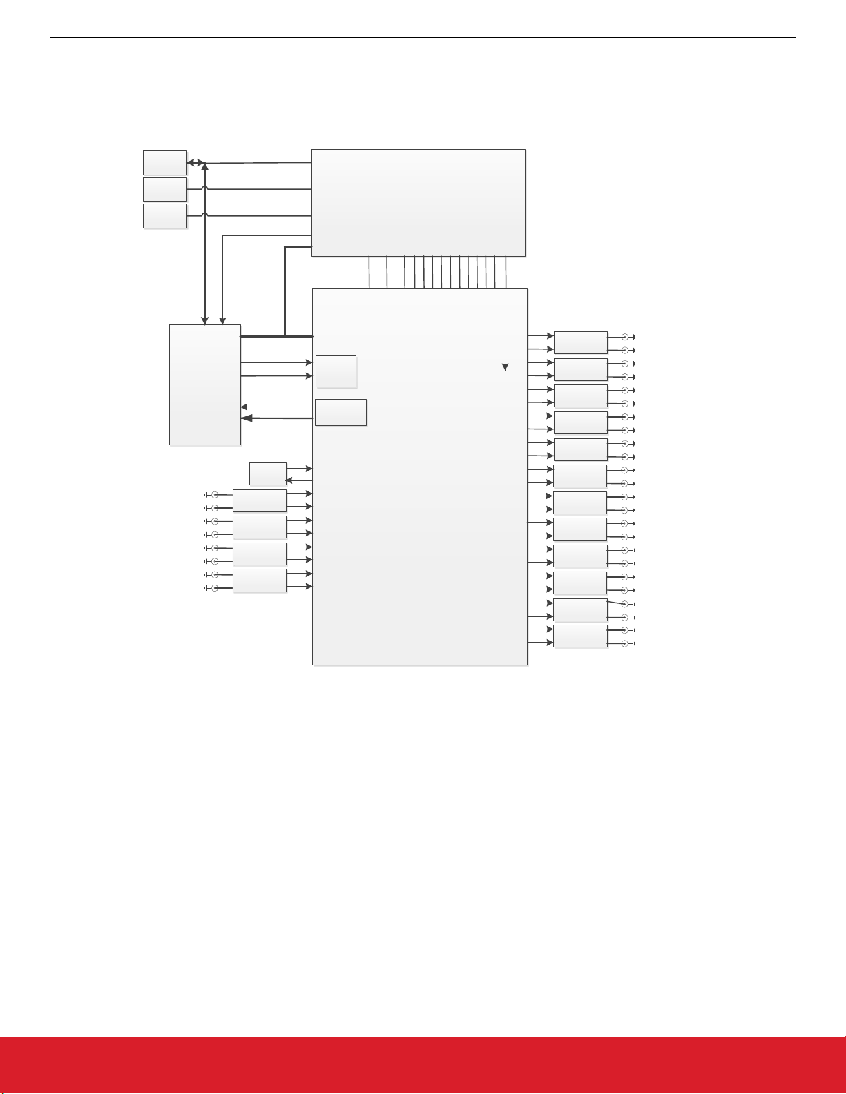
Below is a functional block diagram of the Si5396C EVB. Keep in mind that the Grade L board does not use an external XTAL or reference and does not use the XA/XB pins. This evaluation board can be connected to a PC via the main USB connector for programming,
control, and monitoring. See 3. Quick Start or 10.3 Overview of ClockBuilder Pro Applications for more information.
Main USB
Connector
Aux USB
Connector
Ext +5V
Connector
Input Clock 0
Input Clock 1
Input Clock 2
Input Clock 3
C8051F380
MCU
+
Peripherals
{
{
{
{
Power only
Power only
48 MHz
XTAL
Input
Termination
Input
Termination
Input
Termination
Input
Termination
+5V_USB
+5V_Aux
+5V_Ext
VDDMCU
I2C/SPI Bus
I2C/SPI Bus
Control/
Status
INTR
Alarm_Status
XA
XB
CLKIN_0
CLKIN_0B
CLKIN_1
CLKIN_1B
CLKIN_2
CLKIN_2B
CLKIN_3/FB_IN
CLKIN_3/FB_INB
Power Supply
VDD_3.3
VDD_3.3
VDDO_0
VDDO_1
VDDO_0
VDDO_1
VDDO_0A VDDO_0A
VDD_Core
VDD_Core
Si5396C
VDDO_2
VDDO_3
VDDO_2
VDDO_3
VDDO_4
VDDO_5
VDDO_4
VDDO_5
VDDO_8
VDDO_6
VDDO_7
VDDO_6
VDDO_7
VDDO_8
CLKOUT_0A
CLKOUT_0AB
CLKOUT_0
CLKOUT_0B
CLKOUT_1
CLKOUT_1B
CLKOUT_2
CLKOUT_2B
CLKOUT_3
CLKOUT_3B
CLKOUT_4
CLKOUT_4B
CLKOUT_5
CLKOUT_5B
CLKOUT_6
CLKOUT_6B
CLKOUT_7
CLKOUT_7B
CLKOUT_8
CLKOUT_8B
CLKOUT_9
CLKOUT_9B
CLKOUT_9A
CLKOUT_9AB
VDDO_9
VDDO_9A
VDDO_9
VDDO_9A
Output
Termination
Output
Termination
Output
Termination
Output
Termination
Output
Termination
Output
Termination
Output
Termination
Output
Termination
Output
Termination
Output
Termination
Output
Termination
Output
Termination
Output Clock 0A
}
Output Clock 0
}
Output Clock 1
}
Output Clock 2
}
Output Clock 3
}
Output Clock 4
}
Output Clock 5
}
Output Clock 6
}
Output Clock 7
}
Output Clock 8
}
Output Clock 9
}
Output Clock 9A
}
Figure 1.1. Si5396C EB Functional Block Diagram
silabs.com | Building a more connected world. Rev. 1.0 | 3

UG467: Si5396C/L Evaluation Board User's Guide
Si5396C/L EVB Support Documentation and ClockBuilder Pro Software
2. Si5396C/L EVB Support Documentation and ClockBuilder Pro Software
Si5396C/L EVB schematics, BOMs, user’s guides, and software can be found online www.silabs.com/documents/public/schematic-files/
si539x-design-files.zip
silabs.com | Building a more connected world. Rev. 1.0 | 4

UG467: Si5396C/L Evaluation Board User's Guide
3. Quick Start
1. Install the ClockBuilder Pro desktop software from http://www.silabs.com/CBPro.
2. Connect a USB cable from Si5396C/L EVB to the PC where the software was installed.
3. Confirm jumpers are installed as shown in Table 4.1 Si5396C/L EVB Jumper Defaults1 on page 6.
4. Launch the ClockBuilder Pro Software.
5. You can use ClockBuilder Pro to create, download, and run a frequency plan on the Si5396C/L EVB.
6. Find Si5396 data sheet: https://www.silabs.com/documents/public/data-sheets/si5397-96-a-datasheet.pdf
Quick Start
silabs.com | Building a more connected world. Rev. 1.0 | 5

4. Jumper Defaults
UG467: Si5396C/L Evaluation Board User's Guide
Jumper Defaults
1
I = Installed
0 = Open
Location Type
Table 4.1. Si5396C/L EVB Jumper Defaults
I= Installed
0 = Open
Location Type
JP1 2-pin O JP23 2-pin O
JP2 2-pin I JP24 3-pin All Open
JP3 2-pin O JP25 2-pin O
JP4 2-pin I JP26 3-pin All Open
JP5 2-pin I JP27 2-pin O
JP6 2-pin I JP28 3-pin All Open
JP7 2-pin I JP29 2-pin O
JP8 2-pin O JP30 3-pin All Open
JP9 2-pin O JP31 2-pin O
JP10 2-pin I JP32 3-pin All Open
JP13 2-pin O JP33 2-pin O
JP14 2-pin I JP34 3-pin All Open
JP15 3-pin 1 to 2 JP35 2-pin O
JP16 3-pin 1 to 2 JP36 3-pin All Open
JP17 2-pin O JP38 3-pin All Open
JP18 3-pin All Open JP39 2-pin O
JP19 2-pin O JP40 2-pin O
JP20 3-pin All Open JP41 2-pin O
JP21 2-pin O J36 5 x 2 Hdr All 5 installed
JP22 3-pin All Open
Note:
1.
Refer to the Si5396C/L EVB schematics for the functionality associated with each jumper.
silabs.com | Building a more connected world. Rev. 1.0 | 6

UG467: Si5396C/L Evaluation Board User's Guide
Status LEDs
5. Status LEDs
Location Silkscreen Color Status Function Indication
D27 5VUSBMAIN Blue Main USB +5 V present
D22 3P3V Blue DUT +3.3 V is present
D26 VDD DUT Blue DUT VDD voltage present
D25 INTR Red MCU INTR (Interrupt) active
D21 READY Green MCU Ready
D24 BUSY Green MCU Busy
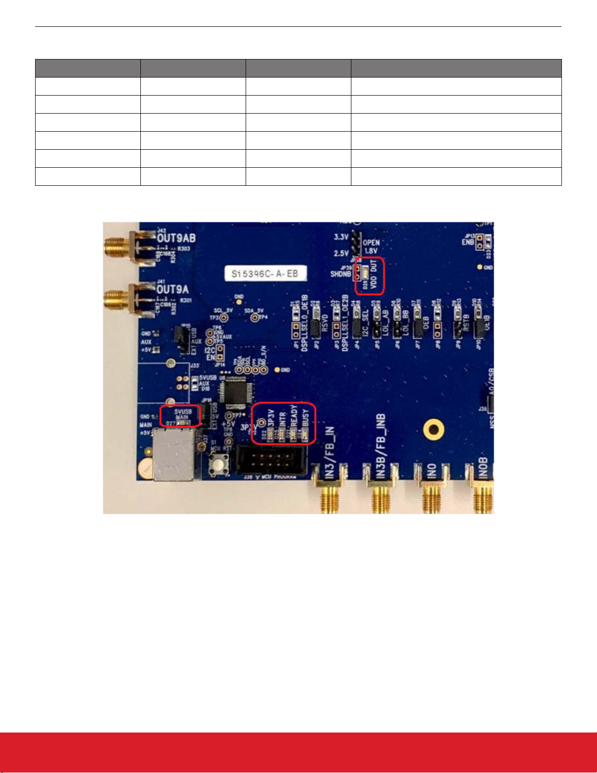
D27, D22, and D26 are illuminated when USB +5 V, Si5396 +3.3 V, and Si5396 VDD supply voltages, respectively, are present. D25,
D21, and D24 are status LEDs showing on-board MCU activity.
Figure 5.1. Status LEDs
silabs.com | Building a more connected world. Rev. 1.0 | 7

UG467: Si5396C/L Evaluation Board User's Guide
External Reference Input (XA/XB)
6. External Reference Input (XA/XB)
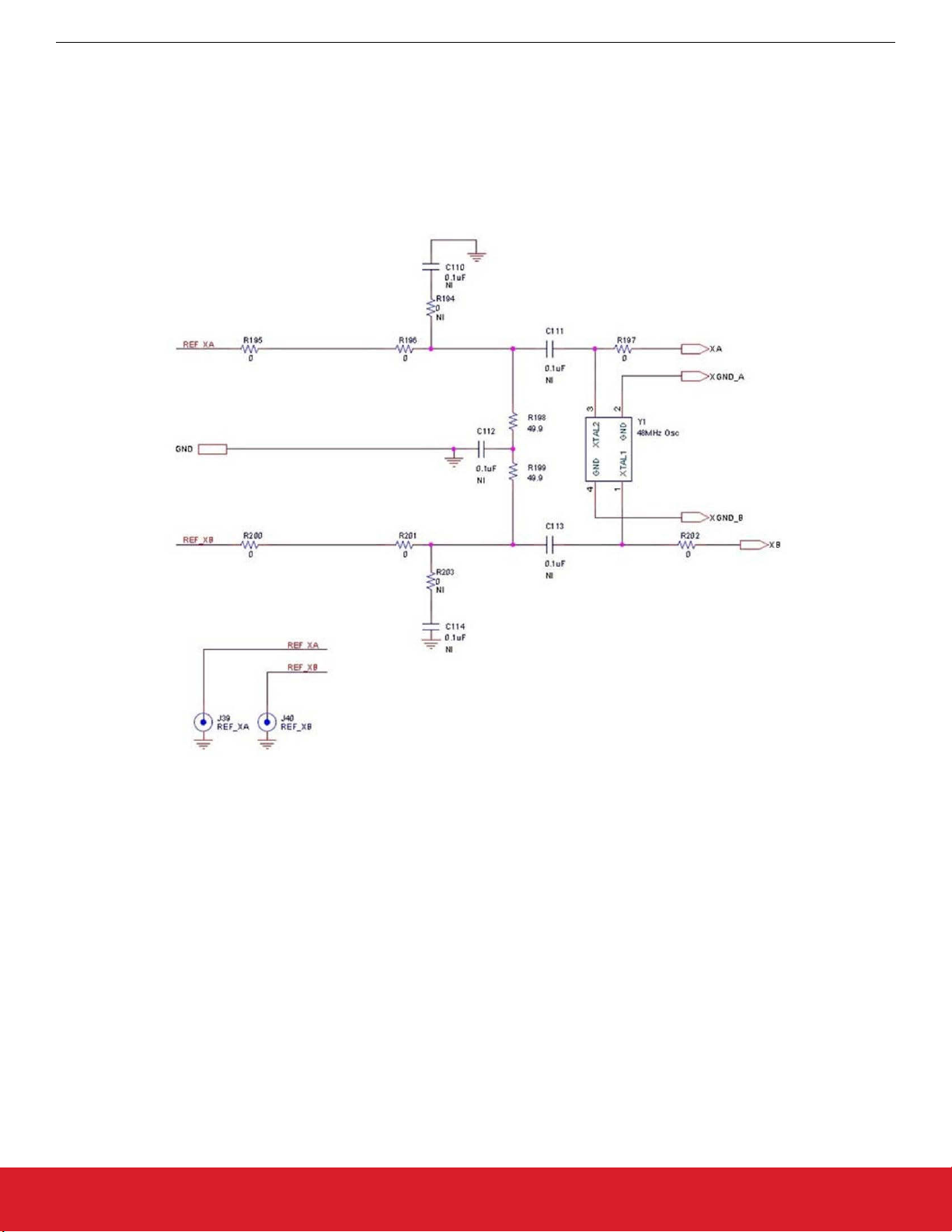
An external reference (XTAL) is required in grade C in combination with the internal oscillator to produce an ultra-low-jitter reference
clock for the DSPLL and to provide a stable reference for the free-run and holdover modes. To evaluate the device with a REFCLK,
C111 and C113 must be populated and the XTAL removed (see the figure below). Also, R197 and R202 must be populated. The
REFCLK can then be supplied to J39 and J40.
Note: For the Si5396L-A, which is the grade with the XTAL internal to the device, there will be no external XTAL supplied on the board
and no input from Ref_XA and Ref_XB. In this case, it is advised that R197 and R202 are removed.
Figure 6.1. External Reference Input Circuit
silabs.com | Building a more connected world. Rev. 1.0 | 8

UG467: Si5396C/L Evaluation Board User's Guide
Clock Input Circuits (INx/INxB)
7. Clock Input Circuits (INx/INxB)
The Si5396C/L EVB has eight SMA connectors (IN0, IN0B – IN3, IN3B) for receiving external clock signals. All input clocks are terminated as shown below. Note that input clocks are ac-coupled and 50 Ω terminated. This represents four differential input clock pairs. Single-ended clocks can be used by appropriately driving one side of the differential pair with a single-ended clock. For details on how to
configure inputs as single-ended, refer to the Si5396 reference manual.
Figure 7.1. Input Clock Termination Circuit
silabs.com | Building a more connected world. Rev. 1.0 | 9
 Loading...