

Page 1

Si5386 Rev. E Reference Manual
Overview
This Reference Manual is intended to provide system, PCB design, signal integrity, and
software engineers the necessary technical information to successfully use the
device in end applications. The official device specifications can be found in the Si5386
datasheet.
The Si5386
is a high-performance, clock generator for small cell applications that demand the highest level of integration and phase noise performance. Based on Silicon
Laboratories’ fourth-generation DSPLL technology, the Si5386 combines frequency synthesis and jitter attenuation in a highly integrated digital solution. A single low phase
noise XO connected to the XA/XB input pins provides the reference for the device. This
all-digital solution provides superior performance that is highly immune to external board
disturbances such as power supply noise.The device configuration is in-circuit program-
mable via an SPI or I2C serial interface and is easily stored in non-volatile memory
(NVM) for applications which require preconfigured clocks at start-up or after reset.
Work Flow Expectations with ClockBuilder™ Pro and the Register Map
This reference manual is to be used to describe all the functions and features of the
parts in the product family with register map details on how to implement them. It is im-
portant to understand that the intent is for customers to use the ClockBuilder™ Pro software to provide the initial configuration for the device. Although the register map is documented, all the details of the algorithms to implement a valid frequency plan are fairly
complex and are beyond the scope of this document. Real-time changes to the frequency plan and other operating settings are supported by the devices. However, describing
all the possible changes is not a primary purpose of this document. Refer to Applications
Notes and Knowledge Base article links within the ClockBuilder Pro GUI for information
on how to implement the most common, real-time frequency plan changes.
Si5386
RELATED DOCUMENTS
• Si5386 Data Sheet
• Si5386
• Si5386A-E-EVB User Guide
• Si5386A-E-EVB Schematics, BOM and
• IBIS models
• To download evaluation board design and
• JESD204B subclass 0 and subclass 1
Device Errata
Layout
support files, see the Si534x/8x Evaluation
Kit
support
silabs.com | Building a more connected world. Rev. 1.0
Page 2

Table of Contents
1. Functional Description............................
1.1 DSPLL.................................5
1.2 LTE Frequency Configuration .........................5
1.3 Configuration for JESD204B Subclass 1 Clock Generation ...............7
1.4 DSPLL Loop Bandwidth ...........................8
1.4.1 Fastlock ...............................8
1.4.2 Holdover Exit Bandwidth .........................9
1.5 Dividers Overview .............................9
2. Modes of Operation ............................10
2.1 Reset and Initialization ...........................11
2.1.1 Updating Registers During Device Operation ..................12
2.1.2 NVM Programming ...........................13
2.2 Free Run Mode ..............................13
2.3 Lock Acquisition Mode ...........................13
2.4 Locked Mode ..............................13
2.5 Holdover Mode ..............................14
5
3. Clock Inputs (IN0, IN1, IN2, IN3) .......................17
3.1 Input Source Selection ...........................17
3.1.1 Manual Input Selection ..........................17
3.1.2 Automatic Input Switching .........................18
3.2 Types of Inputs ..............................19
3.2.1 Hitless Input Switching with Phase Buildout ...................20
3.2.2 Ramped Input Switching .........................21
3.2.3 Glitchless Input Switching .........................21
3.2.4 Unused Inputs.............................21
3.3 Fault Monitoring .............................22
3.3.1 Input LOS (Loss-of-Signal) Detection .....................22
3.3.2 XAXB Reference Clock LOSXAXB (Loss-of-Signal) Detection ............22
3.3.3 Input OOF (Out-of-Frequency) Detection ....................24
3.3.4 DSPLL LOL (Loss-of-Lock) Detection and the LOLb Output Indicator Pin .........26
3.3.5 Device Status Monitoring .........................28
3.3.6 INTRb Interrupt Configuration .......................29
4. Output Clocks ..............................31
4.1 Output Crosspoint Switch ..........................31
4.1.1 Output R Divider Synchronization ......................32
4.2 Performance Guidelines for Outputs .......................33
4.2.1 Optimizing Output Phase Noise .......................34
4.3 Output Signal Format ............................34
4.4 Output Driver Supply Select .........................35
silabs.com | Building a more connected world. Rev. 1.0 | 2
Page 3

4.5 Differential Outputs ............................36
4.5.1 Differential Output Terminations.......................36
4.5.2 Differential Output Amplitude Controls.....................37
4.5.3 Differential Output Common Mode Voltage Selection................37
4.5.4
4.6 LVCMOS Outputs .............................38
4.6.1 LVCMOS Output Terminations .......................39
4.6.2 LVCMOS Output Impedance and Drive Strength Selection..............40
4.6.3 LVCMOS Output Signal Swing .......................40
4.6.4 LVCMOS Output Polarity .........................41
4.7 Output Enable/Disable ...........................42
4.7.1 Output Driver State When Disabled .....................43
4.7.2 Synchronous Output Enable/Disable Feature ..................43
4.7.3 Automatic Output Disable During LOL.....................44
4.7.4 Automatic Output Disable During LOSXAXB ..................44
4.7.5 Output Driver Disable Source Summary ....................45
4.8 Output Delay Control ............................46
Recommended Settings for Differential LVPECL, LVDS, HCSL, and CML ........38
5. Zero Delay Mode .............................47
6. Serial Interface .............................. 49
6.1 I2C Interface ...............................51
6.2 SPI Interface...............................53
7. Field Programming ............................58
8. XAXB External References .........................59
8.1 Performance of External References ......................59
9. XO and Device Circuit Layout Recommendations................. 60
9.1 Si5386 64-Pin QFN External XO Layout Recommendations ...............60
10. Power Management ...........................66
10.1 Power Management Features ........................66
10.2 Power Supply Recommendations .......................66
10.3 Power Supply Sequencing .........................67
10.4 Grounding Vias .............................67
11. Base vs. Factory Preprogrammed Devices ...................68
11.1 "Base" Devices (a.k.a. "Blank" Devices) .....................68
11.2 "Factory Preprogrammed" (Custom OPN) Devices .................68
11.3 Part Numbering Summary..........................68
12. Register Map ..............................69
12.1 Page 0 Registers.............................69
12.2 Page 1 Registers.............................83
12.3 Page 2 Registers.............................90
silabs.com | Building a more connected world. Rev. 1.0 | 3
Page 4

12.4 Page 3 Registers.............................96
12.5 Page 4 Registers.............................98
12.6 Page 5 Registers.............................99
12.7 Page 9 Registers ............................109
12.8 Page A Registers ...........................111
12.9
Page B Registers ...........................113
12.10 Page C Registers ...........................115
13. Appendix—Custom Differential Amplitude Controls ...............116
14. Revision History.............................117
silabs.com | Building a more connected world. Rev. 1.0 | 4
Page 5

Si5386 Rev. E Reference Manual
Functional Description
1. Functional Description
1.1 DSPLL
The DSPLL provides the synthesis for generating the output clock frequencies which are synchronous to the selected input clock frequency or freerun from the reference clock. It consists of a phase detector, a programmable digital loop filter, a high-performance ultralow-phase-noise analog VCO, and a user configurable feedback divider. Use of an external XO provides the DSPLL with a stable lownoise clock source for frequency synthesis and for maintaining frequency accuracy in the Freerun or Holdover modes. No other external
components are required for oscillation. A key feature of DSPLL is providing immunity to external noise coupling from power supplies
and other uncontrolled noise sources that normally exist on printed circuit boards.
The frequency configuration of the DSPLL is programmable through the SPI or I2C serial interface and can also be stored in non-volatile memory (NVM) or RAM. The combination of input dividers (P0-P3), frequency multiplication (M), output division (N), and output division (R0A-R9A) allows the generation of a wide range of frequencies on any of the outputs. All divider values for a specific frequency
plan are easily determined using the ClockBuilder Pro software.
1.2 LTE Frequency Configuration
The device’s frequency configuration is fully programmable through the serial interface and can also be stored in non-volatile memory.
The flexible combination of dividers and a high frequency VCO allows the device to generate multiple output clock frequencies for applications that require ultra-low phase-noise and spurious performance. The table below shows a partial list of possible output frequencies
for LTE applications. The Si5386's DSPLL core can generate up to five unique frequencies. These frequencies are distributed to the
output dividers using a configurable crosspoint mux. The output R dividers allow further division for up to 12 unique integer-related frequencies on the Si5386. The ClockBuilder Pro software utility provides a simple means of automatically calculating the optimum divider
values (P, M, N and R) for the frequencies listed below. In addition to the LTE frequencies, the Si5386 device can simultaneously generate wireline clocks like 156.25 MHz, 155.52 MHz, 125 MHz, etc. and system clocks like 100 MHz, 33 MHz, 25 MHz, etc.
silabs.com | Building a more connected world. Rev. 1.0 | 5
Page 6

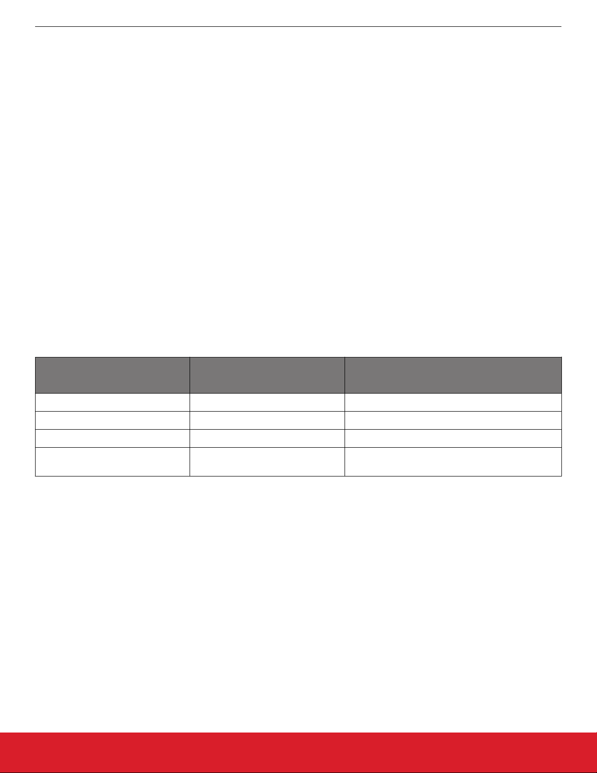
Table 1.1. Example List of Possible LTE Clock Frequencies
Si5386 Rev. E Reference Manual
Functional Description
LTE Device Clock Fout (MHz)
15.36
19.20
30.72
38.40
61.44
76.80
122.88
153.60
184.32
245.76
307.20
368.64
491.52
614.40
737.28
1
983.04
1228.80
1474.56
1638.4
1843.2
2106.51428571
2457.6
2949.12
Note:
1.
R output dividers allow other frequencies to be generated. These
are useful for applications like JESD204B SYSREF clocks.
silabs.com | Building a more connected world. Rev. 1.0 | 6
Page 7
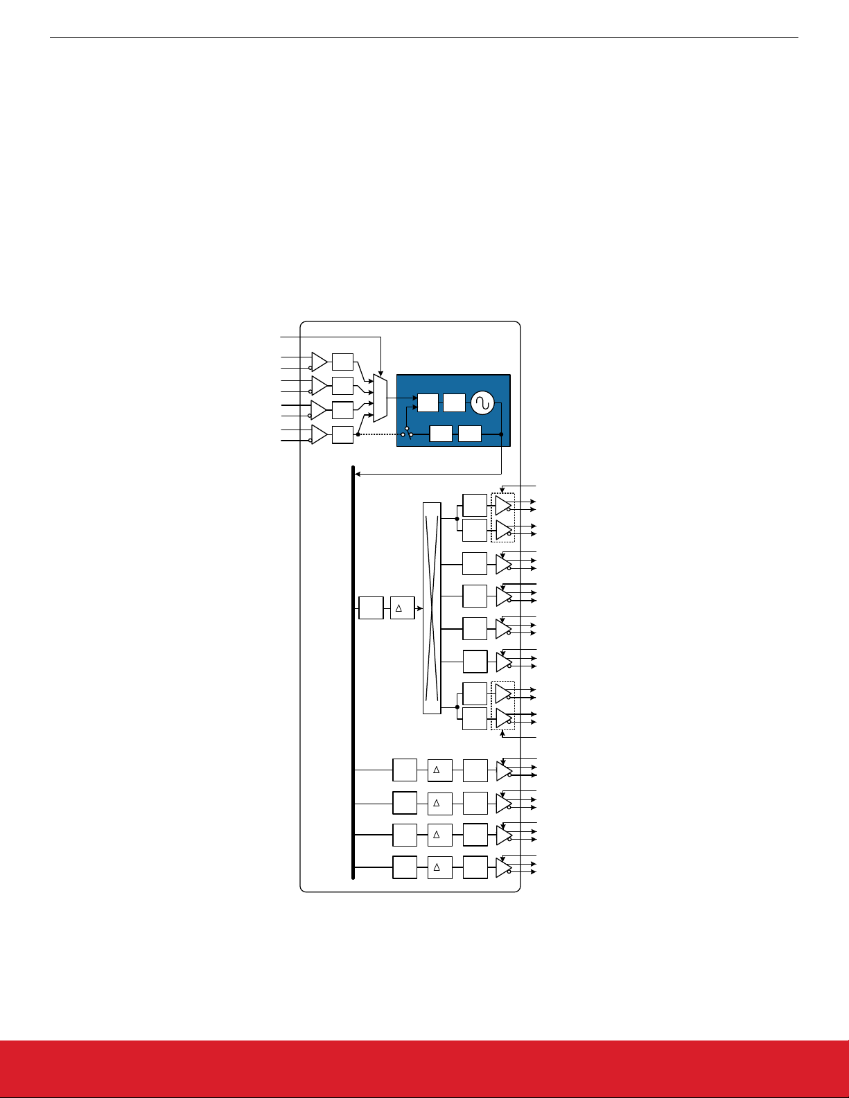
1.3 Configuration for JESD204B Subclass 1 Clock Generation
Si5386 Rev. E Reference Manual
Functional Description
The Si5386
can be used as a high-performance, fully-integrated JEDEC JESD204B jitter cleaner while eliminating the need for discrete
VCXO and loop filter components. The Si5386 supports JESD204B subclass 0 and subclass 1 clocking by providing both device clocks
(DCLK) and system reference clocks (SYSREF). The 12 clock outputs can be independently configured as device clocks or SYSREF
clocks to drive JESD204B ADCs, DACs, FPGAs, or other logic devices. The Si5386 will clock up to six JESD204B subclass 1 targets,
using six DCLK/SYSREF pairs. If SYSREF clocking is implemented in external logic, then the Si5386 can clock up to 12 JESD204B
targets. Not limited to JESD204B applications, each of the 12 outputs is individually configurable as a high performance output for traditional clocking applications.
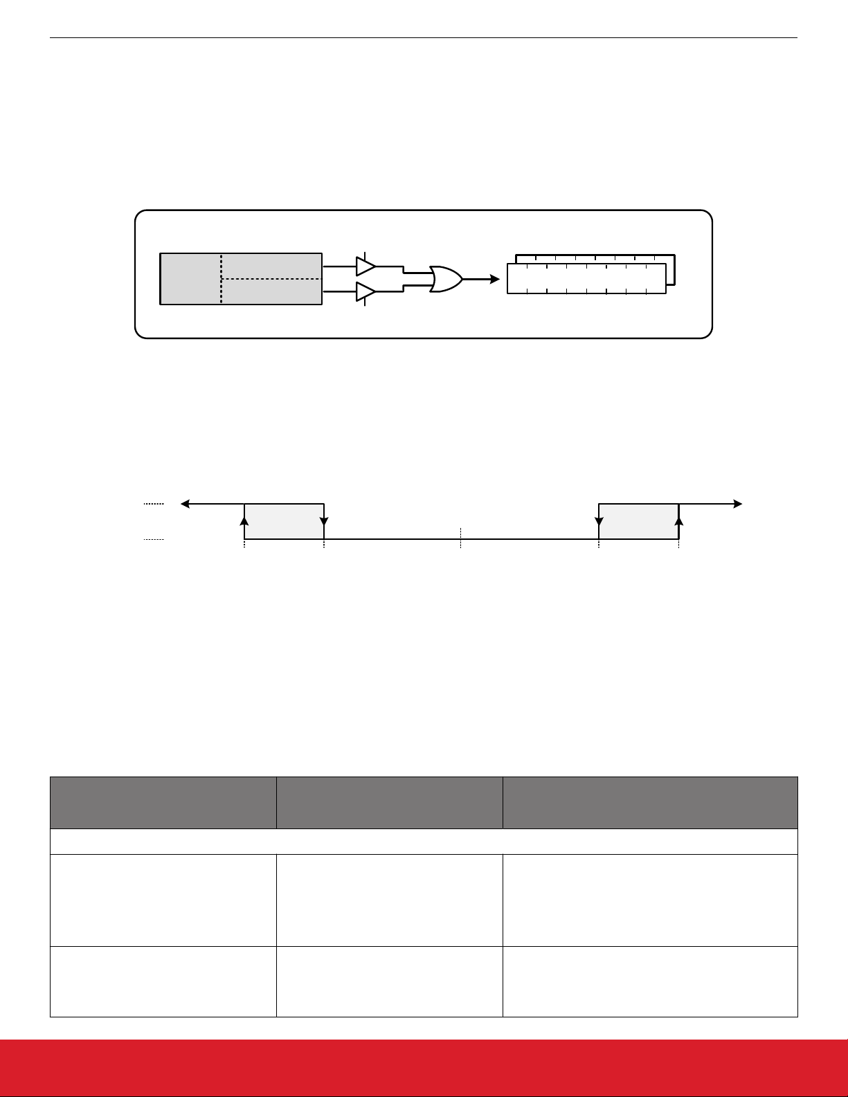
For applications which require adjustable static delay between the DCLK and SYSREF signals, the Si5386 supports up to four DCLK/
SYSREF pairs, each with independently adjustable delay. An example of an adjustable delay JESD204B frequency configuration is
shown in the following figure. In this case, the N0 divider determines the device clock frequencies while the N1-N4 dividers generate the
divided SYSREF used as the lower frequency frame clock. Each output N divider also includes a configurable delay (Δt) for controlling
deterministic latency. This example shows a configuration where all the device clocks are controlled by a single delay (Δt0) while the
SYSREF clocks each have their own independent delay (Δt1 –Δt4), though other combinations are also possible. The bidirectional delay is programmable over ±8.6 ns in 68 ps steps. See 4.8 Output Delay Control for more information on delay control. The SYSREF
clock is always periodic and can be controlled (on/off) without glitches by enabling or disabling its output through register writes.
IN_SEL[1:0]
IN0
IN0b
IN1
IN1b
IN2
IN2b
IN3/FB_IN
IN3b/FB_INb
÷P
÷P
÷P
÷P
0
1
2
3
DSPLL
÷M
LPFPD
÷5
÷N
VDDO0
÷R
0A
÷R
0
÷R
5
÷R
t
0
0
÷N
1
÷N
2
÷N
3
÷N
4
6
÷R
7
÷R
8
÷R
9
÷R
9A
t
1
÷R
1
t
÷R
2
2
t
3
÷R
3
t
4
÷R
4
OUT0A
OUT0Ab
OUT0
OUT0b
VDDO5
OUT5
OUT5b
VDDO6
OUT6
OUT6b
VDDO7
OUT7
OUT7b
VDDO8
OUT8
OUT8b
OUT9
OUT9b
OUT9A
OUT9Ab
VDDO9
VDDO1
OUT1
OUT1b
VDDO2
OUT2
OUT2b
VDDO3
OUT3
OUT3b
VDDO4
OUT4
OUT4b
Device
Clocks
4x SYSREF
Figure 1.1. Si5386 Block Diagram
silabs.com | Building a more connected world. Rev. 1.0 | 7
Page 8

1.4 DSPLL Loop Bandwidth
Si5386 Rev. E Reference Manual
Functional Description
The DSPLL
loop bandwidth determines the amount of input clock jitter attenuation and wander filtering. Register configurable DSPLL
loop bandwidth settings in the range of 1 Hz to 4 kHz are available for selection. Since the loop bandwidth is controlled digitally, the
DSPLL will always remain stable with less than 0.1 dB of peaking regardless of the loop bandwidth selection. The DSPLL loop
bandwidth register values are determined using ClockBuilder Pro.
Note: After manually changing bandwidth parameters, the BW_UPDATE bit must be set high to latch the new values into operation.
This update bit will latch the new values for Loop, Fastlock, and Holdover Exit bandwidths simultaneously.
Table 1.2. DSPLL Loop Bandwidth Registers
Register Name Hex Address
Function
[Bit Field]
BW_PLL 0x0508[7:0]-0x050D[7:0] Determines the loop BW for the DSPLL.
Parameters are generated by ClockBuilder
Pro.
BW_UPDATE 0x0514[0] Writing a 1 to this register bit will latch
Loop, Fastlock, and Holdover Exit BW parameter registers.
1.4.1 Fastlock
Selecting
low DSPLL loop bandwidth (e.g. 1 Hz) will generally lengthen the lock acquisition time. The Fastlock feature allows setting a
a
temporary Fastlock Loop Bandwidth that is used during the lock acquisition process to reduce lock time. Higher Fastlock loop bandwidth settings will enable the DSPLLs to lock faster. Fastlock Bandwidth settings up to 4 kHz are available for selection. Fastlock bandwidth should generally be set from 10x to 100x the loop bandwidth for optimal results. Once lock acquisition has completed, the
DSPLL’s loop bandwidth will automatically revert to the DSPLL Loop Bandwidth setting. The Fastlock feature can be enabled or disabled independently by register control. If enabled, when LOL is asserted Fastlock will be automatically enabled. When LOL is no longer
asserted, Fastlock will be automatically disabled.
Note: The BW_UPDATE_PLLx update bit will latch new values for Loop, Fastlock, and Holdover Exit bandwidths simultaneously.
Table 1.3. DSPLL Fastlock Bandwidth Registers
Register Name Hex Address
Function
[Bit Field]
FASTLOCK_BW_PLL 0x050E[5:0]-0x0513[5:0] Determines the Fastlock BW for the DSPLL. Parameters
are generated by ClockBuilder Pro.
FASTLOCK_AUTO_EN 0x052B[0] Auto Fastlock Enable/Disable.
0: Disable Auto Fastlock (default)
1: Enable Auto Fastlock
FASTLOCK_MAN 0x052B[1] Force Fastlock.
0: Normal Operation (default)
1: Force Fastlock
The loss of lock (LOL) feature is a fault monitoring mechanism. Details of the LOL feature can be found in 3.3.4 DSPLL
Lock) Detection and the LOLb Output Indicator Pin.
LOL
(Loss-of-
silabs.com | Building a more connected world. Rev. 1.0 | 8
Page 9

1.4.2 Holdover Exit Bandwidth
Si5386 Rev. E Reference Manual
Functional Description
In additional
to the Loop and Fastlock bandwidths, a user-selectable bandwidth is available when exiting holdover and locking or relocking to an input clock when ramping is disabled (HOLD_RAMP_BYP = 1). CBPro sets this value equal to the Loop bandwidth by default.
Note that the BW_UPDATE bit will latch new values for Loop, Fastlock, and Holdover bandwidths simultaneously.
Table 1.4. DSPLL Holdover Exit Bandwidth Registers
Register Name Hex Address
Function
[Bit Field]
HOLDEXIT_BW 0x059D[5:0]–0x05A2[5:0] Determines the Holdover Exit BW for the
DSPLL. Parameters are generated by
ClockBuilder Pro.
1.5 Dividers Overview
There are
four divider classes within the Si5386. Figure 1.1 Si5386 Block Diagram on page 7 shows all of these dividers. All divider
values for the Si5386 may be either Fractional or Integer. For best phase noise performance, integer dividers are preferred..
• P0-P3: Input clock wide range dividers (0x0208–0x022F)
• 48-bit numerator, 32-bit denominator
•
Min. value is 1; Max. value is 224 (Fractional-P divisors must be > 5)
• Practical range limited by phase detector and VCO range
• Each divider has an update bit that must be written to cause a newly written divider value to take effect.
• Soft Reset All will also update the P divider values
• M: DSPLL feedback divider (0x0515–0x051F)
• 56-bit numerator, 32-bit denominator
•
Min. value is 5, Max. value is 224 (Fractional-M divisors must be > 10)
• Practical range limited by phase detector and VCO range
• The M divider has an update bit that must be written to cause a newly written divider value to take effect.
• Soft Reset will also update M divider values.
• The DSPLL includes an additional divide-by-5 in the feedback path. Manually calculated M divider register values must be adjusted accordingly.
• N: Output divider (0x0302-0x0338)
• 44-bit numerator, 32-bit denominator
•
Min. value is 5, Max. value is 224 (Fractional-M divisors must be > 10)
• Each N divider has an update bit that must be written to cause a newly written divider value to take effect.
• Soft Reset will also update N divider values.
• R: Final output divider (0x0247-0x026A)
• 24-bit field
•
Min. value is 2, Max. value is 225-2
• Only even integer divide values: 2,4,6, etc.
• R Divisor=2 x (Field +1). For example, Field=3 gives an R divisor of 8.
silabs.com | Building a more connected world. Rev. 1.0 | 9
Page 10
Si5386 Rev. E Reference Manual
Modes of Operation
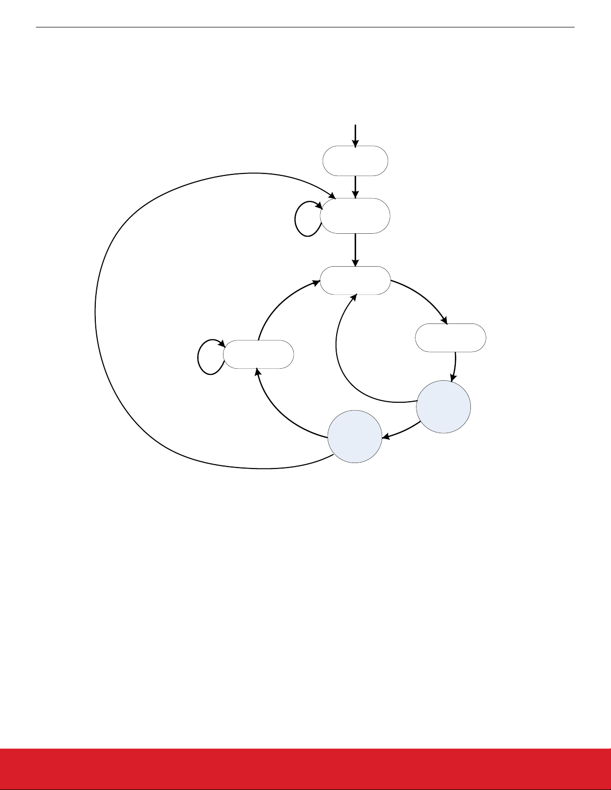
2. Modes of Operation
After initialization, the DSPLL will operate in one of the following modes: Free-run, Lock-Acquisition, Locked, or Holdover. These modes
are described further in the sections below.
Power-Up
Reset and
Initialization
No valid input
clocks available
for selection
No valid
input clocks
selected
An input is
qualified and
available for
selection
Holdover
Mode
Free-run
Lock Acquisition
(Fast Lock)
Input Clock
Yes
Holdover
History
Valid?
No
Valid input clock
selected
Switch
Yes
No
Phase lock on
selected
is achieved
clock
Locked
Mode
Other Valid
Clock Inputs
Available?
input
Selected input
clock
fails
Figure 2.1. Modes of Operation
silabs.com | Building a more connected world. Rev. 1.0 | 10
Page 11
2.1 Reset and Initialization
Si5386 Rev. E Reference Manual
Modes of Operation
Once power
is applied, the device begins an initialization period where it downloads default register values and configuration data from
NVM and performs other initialization tasks. Communicating with the device through the SPI or I2C serial interface is possible once this
initialization period is complete. No output clocks will be generated until the initialization is complete.
There are two types of resets available. A Hard Reset is functionally similar to a device power-up. All registers will be restored to the
values stored in NVM, and all circuits including the serial interface, will be restored to their initial state. A Hard Reset is initiated using
the RSTb pin or by asserting the Hard Reset bit. A Soft Reset bypasses the NVM download and is used to initiate in-system register
configuration changes. The table below lists the reset and control registers.
Table 2.1. Reset Registers
Register Name Hex Address
Function
[Bit Field]
HARD_RST 0x001E[1] Writing a 1 to this register bit performs the same func-
tion as power cycling the device. All registers will be
restored to their NVM values.
SOFT_RST 0x001C[0] Writing a 1 to this register bit performs a Soft Reset of
the device. Initiates register configuration changes
without reloading NVM.
Power-Up
Hard Reset bit
asserted
RSTb
pin asserted
NVM download
Soft Reset bit
asserted
Initialization
Serial interface ready
Figure 2.2. Initialization from Hard Reset and Soft Reset
The Si5386 is
configurable using the serial interface (I2C or SPI). At power up the device downloads its default register values from
fully
internal non-volatile memory (NVM). Application specific default configurations can be written into NVM allowing the device to generate
specific clock frequencies at power-up. Writing default values to NVM is in-circuit programmable with normal operating power supply
voltages applied to its VDD and VDDA pins.
silabs.com | Building a more connected world. Rev. 1.0 | 11
Page 12
2.1.1 Updating Registers During Device Operation
Si5386 Rev. E Reference Manual
Modes of Operation
If certain
registers are changed while the device is in operation, it is possible for the PLL to become unresponsive (i.e. lose lock indefinitely). Any change that causes the VCO frequency to change by more than 250 ppm since Power-up, NVM download, or SOFT_RST
requires the following special sequence of writes. The following are the affected registers:
Control Register(s)
P0_NUM / P0_DEN 0x0208 – 0x0211
P1_NUM / P1_DEN 0x0212 – 0x021B
P2_NUM / P2_DEN 0x021C – 0x0225
P3_NUM / P3_DEN 0x0226 – 0x022F
Px_UPDATE 0x0230
P0_FRACN_MODE / P0_FRAC_EN 0x0231
P1_FRACN_MODE/ P1_FRAC_EN 0x0232
P2_FRACN_MODE / P2_FRAC_EN 0x0233
P3_FRACN_MODE/ P3_FRAC_EN 0x0234
MXAXB_NUM / MXAXB_DEN 0x0235 – 0x023E
MXAXB_UPDATE 0x023F
PLL lockup can easily be avoided by using the following the preamble and postamble write sequence when one of these registers is
modified during
device operation. ClockBuilder Pro software adds these writes to the output file by default when Exporting Register
Files.
1. To start, write the preamble by updating the following control bits using Read/Modify/Write sequences:
Register Value
0x0B24 0xC0
0x0B25 0x00
0x0540 0x01
2. Wait 625 ms for the device state to stabilize.
3. Then modify all desired control registers.
4.
Write 0x01 to Register 0x001C (SOFT_RST) to perform a Soft Reset once modifications are complete.
5. Write the postamble by updating the following control bits using Read/Modify/Write sequences:
Register Value
0x0540 0x00
0x0B24 0xC3
0x0B25 0x02
silabs.com | Building a more connected world. Rev. 1.0 | 12
Page 13
2.1.2 NVM Programming
Si5386 Rev. E Reference Manual
Modes of Operation
The NVM
is two-time writable by the user. Once a new configuration has been written to NVM, the old configuration is no longer acces-
sible.
While polling DEVICE_READY during the procedure below, the following conditions must be met in order to ensure that the correct
values are written into the NVM:
• VDD and VDDA power must both be stable throughout the process.
• No additional registers may be written during the polling. This includes the page register at address 0x01. DEVICE_READY is available on every register page, so no page change is needed to read it.
• Only the DEVICE_READY register (0xFE) should be read during this time.
The procedure for writing registers into NVM is as follows:
1. Write all registers as needed. Verify device operation before writing registers to NVM.
2. You may write to the user scratch space (registers 0x026B to 0x0272) to identify the contents of the NVM bank.
3. Write 0xC7 to NVM_WRITE register.
4. Poll DEVICE_READY until DEVICE_READY=0x0F.
5. Set NVM_READ_BANK 0x00E4[0]=1.
6. Poll DEVICE_READY until DEVICE_READY=0x0F.
Alternatively, Steps 5 and 6 can be replaced with a Hard Reset, either by RSTb pin, HARD_RST register bit, or power cycling the device to generate a POR. All of these actions will load the new NVM contents back into the device registers.
Note that the I2C_ADDR setting in register 0x000B is not saved as part of this NVM write procedure. To update this register in a nonvolatile way, the "Si534x8x I2C Address Burn Tool" allows updating this value one time. This utility is included in the ClockBuilder Pro
installation and can be accessed under the "Misc" folder in the installation directory.
Table 2.2. NVM Programming Registers
Register Name Hex Address
Function
[Bit Field]
ACTIVE_NVM_BANK 0x00E2[7:0] Identifies the active NVM bank.
NVM_WRITE 0x00E3[7:0] Initiates an NVM write when written with value 0xC7.
NVM_READ_BANK 0x00E4[0] Download register values with content stored in NVM.
DEVICE_READY 0x00FE[7:0] Indicates that the device is ready to accept com-
mands when value = 0x0F.
2.2 Free Run Mode
Once power
is applied to and initialization is complete the DSPLL will automatically enter Freerun mode, generating the output frequencies determined by the NVM. The frequency accuracy of the generated output clocks in Freerun mode is entirely dependent on the
frequency accuracy of the XAXB reference clock. Any temperature drift of this frequency will be tracked at the output clock frequencies.
A TCXO or OCXO is recommended for applications that need better frequency accuracy and lower wander while in Freerun or Holdover modes. Since there is little jitter attenuation from the XAXB pins to the clock outputs, devices should use a low-jitter XAXB reference clock to minimize output clock jitter.
2.3 Lock Acquisition Mode
The device monitors all inputs for a valid clock. If a valid clock is available for synchronization, the DSPLL will automatically start the
lock acquisition process. If the Fastlock feature is enabled, the DSPLL will acquire lock using the Fastlock Loop Bandwidth setting and
then transition to the DSPLL Loop Bandwidth setting when lock acquisition is complete. During lock acquisition the outputs will generate
a clock that follows the VCO frequency change as it pulls-in to the input clock frequency.
2.4 Locked Mode
Once locked, the DSPLL will generate output clocks that are both frequency and phase locked to its selected input clock. At this point,
the XAXB reference clock frequency drift does not affect the output frequency. A loss of lock pin (LOLb) and status bit indicate when
lock is achieved. See 3.3.4 DSPLL LOL (Loss-of-Lock) Detection and the LOLb Output Indicator Pin for more details on the operation of
the loss of lock circuit.
silabs.com | Building a more connected world. Rev. 1.0 | 13
Page 14
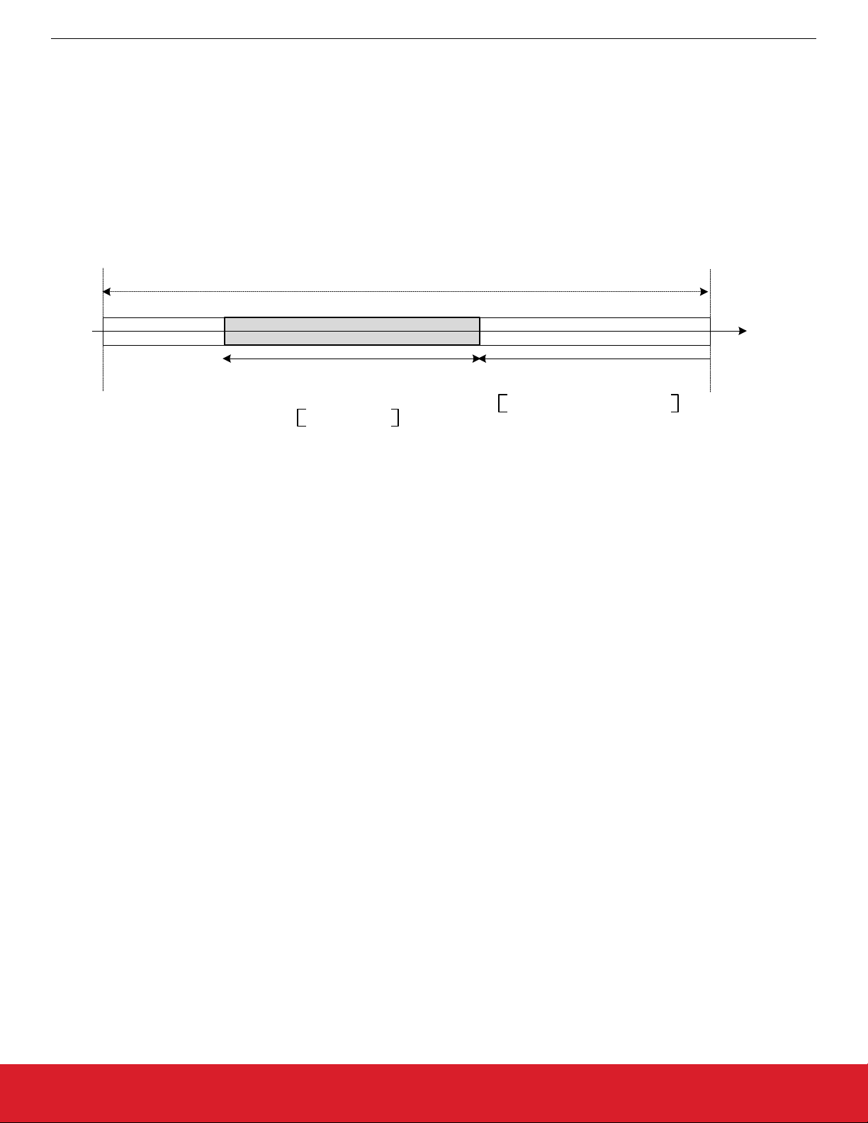
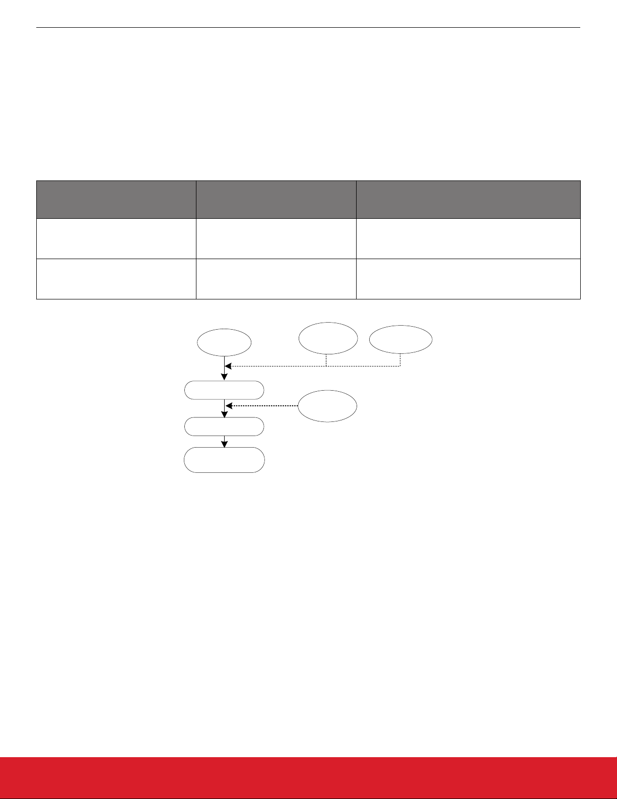
2.5 Holdover Mode
Si5386 Rev. E Reference Manual
Modes of Operation
The DSPLL
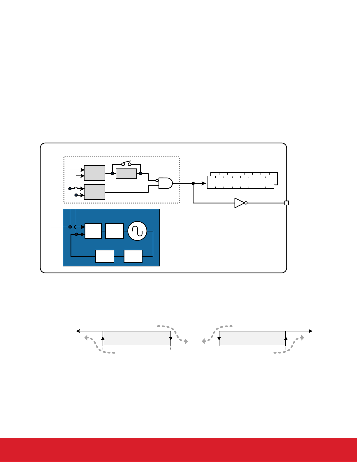
will automatically enter Holdover mode when the selected input clock becomes invalid and no other valid input clocks are
available for selection. It uses an averaged input clock frequency as its final holdover frequency to minimize the disturbance of the output clock phase and frequency when an input clock suddenly fails. The holdover circuit stores up to 120 seconds of historical frequency
data while locked to a valid clock input. The final averaged holdover frequency value is calculated from a programmable window within
the stored historical frequency data. Both the window size and the delay are programmable as shown in the figure below. The window
size determines the amount of holdover frequency averaging. This delay value allows recent frequency information to be ignored for
Holdover in cases where the input clock source frequency changes as it is removed.
Clock Failure
and Entry into
Holdover
Historical Frequency Data Collected
time
120s
Programmable historical data window
used to
determine the final holdover value
1s,10s, 30s, 60s
Programmable delay
30ms, 60ms, 1s,10s, 30s, 60s
0s
Figure 2.3. Programmable Holdover Window
When entering Holdover, the DSPLL will pull its output clock frequency to the calculated averaged holdover frequency. While in Holdover, the output frequency drift is determined by the reference clock temperature drift. If a clock input becomes valid, the DSPLL will
automatically exit the Holdover mode and reacquire lock to the new input clock. This process involves pulling the output clock frequency
to achieve frequency and phase lock with the input clock. This pull-in process is Glitchless and its rate is controlled by the DSPLL bandwidth or the Fastlock bandwidth, if Fastlock is enabled. These options are register programmable.
The recommended mode of exit from holdover is a ramp in frequency. Just before the exit begins, the frequency difference between the
output frequency while in holdover and the desired, new output frequency is measured. It is quite possible that the new output clock
frequency will not be exactly the same as the holdover output frequency because the new input clock frequency might have changed
and the holdover history circuit may have changed the holdover output frequency. The ramp logic calculates the difference in frequency
between the holdover frequency and the new, desired output frequency. Using the user selected ramp rate, the correct ramp time is
calculated. The output ramp rate is then applied for the correct amount of time so that when the ramp ends, the output frequency will be
the desired new frequency. Using the ramp, the transition between the two frequencies is smooth and linear. The ramp rate can be
selected to be very slow (0.2 ppm/sec), very fast (40,000 ppm/sec) or any of approximately 40 values that are in between. The loop BW
values do not limit or affect the ramp rate selections and vice versa. CBPro defaults to ramped exit from holdover. Ramping is also used
for ramped input clock switching. See 3.2.2 Ramped Input Switching for more information. See AN1057: Hitless Switching using
Si534x/8x Devices for more information on Hitless and Ramped Switching with Rev. E devices.
As shown in Figure 2.1 Modes of Operation on page 10 the Holdover and Freerun modes are closely related. The device will only enter
Holdover if a valid clock has been selected long enough for the holdover history to become valid, i.e., HOLD_HIST_VALID = 1. If the
clock fails before the combined HOLD_HIST_LEN + HOLD_HIST_DELAY time has been met, HOLD_HIST_VALID = 0 and the device
will enter Freerun mode instead. Note that when switching between input clocks with different (non-0 ppm offset) frequencies, the holdover history requires a time of 2 * HOLD_HIST_LEN + HOLD_HIST_DELAY to update the average frequency value. If a switch is initiated before this time, the average holdover frequency will be a value between the old input frequency and the new one.
Note: The Holdover history accumulation is suspended when the input clock is removed and resumes accumulating when a valid input
clock is again presented to the DSPLL.
silabs.com | Building a more connected world. Rev. 1.0 | 14
Page 15

Table 2.3. Holdover Mode Control Registers
Si5386 Rev. E Reference Manual
Modes of Operation
Register Name Hex Address
Function
[Bit Field]
Holdover Status
HOLD 0x000E[5] DSPLL Holdover status indicator.
0: Normal Operation
1: In Holdover/Freerun Mode:
HOLD_HIST_VALID = 0 ≥ Freerun Mode
HOLD_HIST_VALID = 1 ≥ Holdover Mode
HOLD_FLG 0x0013[5] Holdover indicator sticky flag bit. Remains asserted after the indi-
cator bit shows a fault until cleared by the user. Writing a 0 to the
flag bit will clear it if the indicator bit is no longer asserted.
HOLD_INTR_MSK 0x0019[5] Masks Holdover/Freerun from generating INTRb interrupt.
0: Allow Holdover/Freerun interrupt (default)
1: Mask (ignore) Holdover/Freerun for interrupt
HOLD_HIST_VALID 0x053F[1] Holdover historical frequency data valid.
0: Incomplete Holdover history, Freerun mode available
1: Valid Holdover history, Holdover mode available
Holdover Control and Settings
HOLD_HIST_LEN 0x052E[4:0] Window Length time for historical average frequency used in
Holdover mode. Window Length in seconds (s):
Window Length = (2
HOLD_HIST_LEN
- 1) x 8 / 3 x 10
HOLD_HIST_DELAY 0x052F[4:0] Delay Time to ignore data for historical average frequency in
Holdover mode. Delay Time in seconds (s):
Delay Time = 2
HOLD_HIST_DELAY
x 2 / 3 x 10
-7
FORCE_HOLD 0x0535[0] Force the device into Holdover mode. Used to hold the device
output clocks while retraining an upstream input clock.
0: Normal Operation
1: Force Holdover/Freerun Mode:
HOLD_HIST_VALID = 0 =>Freerun Mode
HOLD_HIST_VALID = 1 =>Holdover Mode
Holdover Exit Control
HOLD_RAMP_BYP 0x052C[3] Holdover Exit Ramp Bypass
0: Use Ramp when exiting from Holdover (default)
1: Use Holdover/Fastlock/Loop bandwidth when exiting from Holdover
-7
silabs.com | Building a more connected world. Rev. 1.0 | 15
Page 16

Si5386 Rev. E Reference Manual
Modes of Operation
Register Name Hex Address
Function
[Bit Field]
HOLDEXIT_BW_SEL0 0x059B[6] Select the exit bandwidth from Holdover when ramped exit is not
selected (HOLD_RAMP_BYP = 1).
00: Use Fastlock bandwidth on Holdover exit
01: Use Holdover Exit bandwidth on Holdover exit (default)
10, 11: Use Normal Loop bandwidth on Holdover exit
HOLDEXIT_BW_SEL1 0x052C[4] Select the exit bandwidth from Holdover when ramped exit is not
selected (HOLD_RAMP_BYP = 1).
00: Use Fastlock bandwidth on Holdover exit
01: Use Holdover Exit bandwidth on Holdover exit (default)
10, 11: Use Normal Loop bandwidth on Holdover exit
RAMP_STEP_INTERVAL 0x052C[7:5] Time Interval of the frequency ramp steps when ramping between
inputs or exiting holdover.
RAMP_STEP_SIZE 0x05A6[2:0] Size of the frequency ramp steps when ramping between inputs
or exiting holdover.
silabs.com | Building a more connected world. Rev. 1.0 | 16
Page 17

Si5386 Rev. E Reference Manual
Clock Inputs (IN0, IN1, IN2, IN3)
3. Clock Inputs (IN0, IN1, IN2, IN3)
3.1 Input Source Selection
The inputs accept both standard format inputs and DC coupled CMOS clocks. Input selection from CLK_SWITCH_MODE can be manual (pin or register controlled) or automatic with user definable priorities. Register bit 0x052A[0] (IN_SEL_REG_CTRL) is used to select
manual pin or register control, and to configure the input as shown in the table below.
Table 3.1. Input Selection Control Registers
Register Name Hex Address
CLK_SWITCH_MODE 0x0536[1:0] Selects manual or automatic switching modes. Automatic
IN_SEL_REGCTRL 0x052A[0] Manual Input Select control source.
IN_SEL 0x052A[3:1] Manual Input Select selection register.
.
3.1.1 Manual Input Selection
In manual mode, CLK_SWITCH_MODE=0x00.
Function
[Bit Field]
mode can be Revertive or Non-revertive. Selections are the
following:
00: Manual (default)
01: Automatic Non-revertive
02: Automatic Revertive
03: Reserved
0: Pin controlled input clock selection (default)
1: IN_SEL register input clock selection
0: IN0 (default), 1: IN1, 2: IN2, 3: IN3/FB_IN, 4-7: Reserved
Input switching
can be done manually using the IN_SEL[1:0] device pins from the package or through register 0x052A IN_SEL[2:1]. Bit
0 of register 0x052A determines if the input selection is pin selectable or register selectable. The default is pin selectable. The following
table describes the input selection on the pins. Note that when Zero Delay Mode is enabled, the FB_IN pins will become the feedback
input and IN3 therefore is not available as a clock input. If there is not a valid clock signal on the selected input, the device will automatically enter Freerun or Holdover mode. See Chapter 5. Zero Delay Mode for further information.
Table 3.2. Manual Input Selection using IN_SEL[1:0] Pins
IN_SEL[1:0] PINS DSPLL Input Source
00 IN0
01 IN1
10 IN2
11
IN3
1
Note:
1.
IN3 not available as a DSPLL source in ZDM.
silabs.com | Building a more connected world. Rev. 1.0 | 17
Page 18

3.1.2 Automatic Input Switching
In automatic mode CLK_SWITCH_MODE = 0x01 (Non-revertive) or 0x02 (Revertive).
Si5386 Rev. E Reference Manual
Clock Inputs (IN0, IN1, IN2, IN3)
Automatic input
switching is available in addition to the manual selection described previously in 3.1.1 Manual Input Selection. In automatic mode, the switching criteria is based on input clock qualification, input priority and the revertive option. The IN_SEL[0/1] pins and
IN_SEL 0x052A[3:1] register bits are not used in automatic input switching. Also, only input clocks that are valid (i.e., with no active fault
indicators) can be selected by the automatic clock switching. If there are no valid input clocks available, the DSPLL will enter Holdover
or Freerun mode. With Revertive switching enabled, the highest priority input with a valid input clock is always selected. If an input with
a higher priority becomes valid then an automatic switchover to that input will be initiated. With Non-revertive switching, the active input
will always remain selected while it is valid. If it becomes invalid, an automatic switchover to the highest priority valid input will be initiated. Note that automatic input switching is not available in Zero Delay Mode. See section 5. Zero Delay Mode for further information.
Table 3.3. Automatic Input Switching Registers
Register Name Hex Address
Function
[Bit Field]
IN_LOS_MSK 0x0537[3:0] Enables the use of IN3 - IN0 LOS status in determining a val-
id clock for automatic input selection.
0: Use LOS in automatic clock switching logic (default)
1: Mask (ignore) LOS from the automatic clock switching logic
IN_OOF_MSK 0x0537[7:4] Determines the OOF status for IN3 - IN0 and is used in de-
termining a valid clock for the automatic input selection.
0: Use OOF in the automatic clock switching logic (default)
1: Mask (ignore) OOF from the automatic clock switching logic
IN0_PRIORITY 0x0538[2:0] IN0 - IN3 priority assignment for the automatic switching
IN1_PRIORITY 0x0538[6:4]
IN2_PRIORITY 0x0539[2:0]
IN3_PRIORITY 0x0539[6:4]
state machine. Priority assignments in descending importance are:
1, 2, 3, 4, or 0 for never selected
5-7: Reserved
silabs.com | Building a more connected world. Rev. 1.0 | 18
Page 19
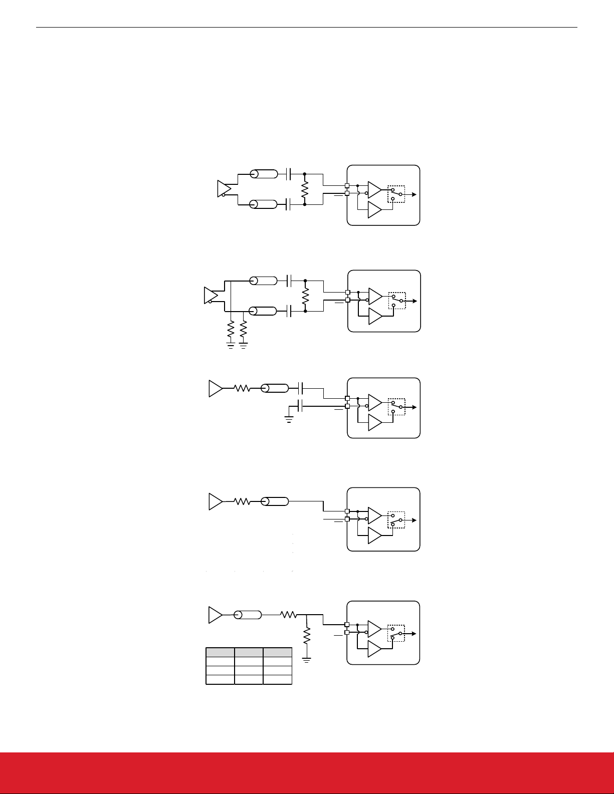
3.2 Types of Inputs
Si5386 Rev. E Reference Manual
Clock Inputs (IN0, IN1, IN2, IN3)
Each of
the four different inputs IN0-IN3/FB_IN can be configured as standard LVDS, LVPECL, HCL, CML, and AC-coupled singleended LVCMOS formats, or as DC-coupled CMOS format. The standard format inputs have a nominal 50% duty cycle, must be accoupled and use the “Standard” Input Buffer selection as these pins are internally dc biased to approximately 0.83 V. The pulsed CMOS
input format allows pulse-based inputs, such as frame-sync and other synchronization signals, having a duty cycle much less than 50%.
These pulsed CMOS signals are dc-coupled and use the “Pulsed CMOS” Input Buffer selection. In all cases, the inputs should be terminated near the device input pins as shown in the figure below. The resistor divider values given below will work with up to 1 MHz pulsed
inputs. In general, following the “Standard AC Coupled Single Ended” arrangement shown below will give superior jitter performance
over Pulsed CMOS.
Standard AC Coupled Differential LVDS
Si5386
3.3V, 2.5V
L
VDS or CML
50
50
INx
100
INx
Standard
Pulsed CMOS
Standard AC Coupled Differential LVPECL
Si5386
3.3V, 2.5V
LVPECL
50
50
INx
100
INx
Standard
Pulsed CMOS
3.3V, 2.5V, 1.8V
LVCMOS
3.3V, 2.5V, 1.8V
LVCMOS
IN_CMOS_USE1P8 = 1, at address 0x094F
Pulsed CMOS DC Coupled Single Ended
3.3V, 2.5V, 1.8V
LVCMOS
VDD R1 ( ) R2 ( )
1.8V 324 665
2.5V 511 475
3.3V 634 365
Standard AC Coupled Single Ended
50
INx
INx
DC Coupled CMOS
50
50
R1
R
2
INx
X
INx
INx
INx
Standard
Pulsed CMOS
Standard
CMOS
Standard
Pulsed CMOS
Si5386
Si5386
Si5386
Figure 3.1. Input Termination for Standard and CMOS Inputs
silabs.com | Building a more connected world. Rev. 1.0 | 19
Page 20

Si5386 Rev. E Reference Manual
Clock Inputs (IN0, IN1, IN2, IN3)
Input clock buffers are enabled by setting the IN_EN 0x0949[3:0] bits appropriately for IN3 through IN0. Unused clock inputs may be
powered down
shown in the figure above, including the “Standard AC Coupled Single Ended” case. In Pulsed CMOS mode, it is not necessary to connect the inverting INb input pin. To place the input buffer into Pulsed CMOS mode, the corresponding bit must be set in
IN_PULSED_CMOS_EN 0x0949[7:4] for IN3 through IN0.
and left unconnected at the system level. For standard mode inputs, both input pins must be properly connected as
Table 3.4. Input Clock Configuration Registers
Register Name Hex Address
Function
[Bit Field]
IN_EN 0x0949[3:0] Enable (or powerdown) the IN3 – IN0 input buffers.
0: Powerdown input buffer
1: Enable and Power-up input buffer
IN_PULSED_CMOS_EN 0x0949[7:4] Select Pulsed CMOS input buffer for IN3 – IN0.
0: Standard Input Format (default)
1: Pulsed CMOS Input Format
CMOS_HI_THR 0x094F[7:4] CMOS Clock input threshold select for inputs IN3 - IN0.
0: Low threshold (Pulsed CMOS)
1: Standard Threshold - Use with 1.8 V CMOS input clocks
3.2.1 Hitless Input Switching with Phase Buildout
Hitless Switching
is a feature that prevents the phase of an output clock from changing when switching to a new input clock that does
not have the same phase as the original input clock. It only makes sense to enable phase buildout when switching between two clocks
that are exactly the same frequency (i.e. are frequency locked). When hitless switching phase buildout is enabled (register 0x0536[2] =
1), the DSPLL absorbs the phase difference between the current input clock and the new input clock. When disabled (register
0x0536[2] = 0), the phase difference between the two input clocks will propagate to the output at a rate that is determined by the
DSPLL loop bandwidth. Phase buildout hitless switching supports clock frequencies down to the minimum input frequency. Note that
Hitless switching is not available in Zero Delay Mode. Input switching events on DSPLL B may affect the outputs of the other A/C/D
DSPLLs. See AN1057: Hitless Switching using Si534x/8x Devices for more information on Hitless and Ramped Switching with Rev. E
devices.
Table 3.5. Input Hitless Switching
Register Name Hex Address
Function
[Bit Field]
HSW_EN 0x0536[2] Enable Hitless Switching.
0: Disable Hitless switching
1: Enable Hitless switching (phase buildout enabled) (default)
silabs.com | Building a more connected world. Rev. 1.0 | 20
Page 21

3.2.2 Ramped Input Switching
Si5386 Rev. E Reference Manual
Clock Inputs (IN0, IN1, IN2, IN3)
The DSPLL
has the ability to switch between two input clock frequencies that are up to ±20 ppm apart. When switching between input
clocks that are not exactly the same frequency (i.e. are plesiochronous), ramped switching should be enabled to ensure a smooth transition between the two input frequencies. In this situation, it is also advisable to enable hitless switching phase buildout to minimize the
input-to-output clock skew after the clock switch ramp has completed. See AN1057: Hitless Switching using Si534x/8x Devices for more
information on Hitless and Ramped Switching with Rev. E devices.
When ramped clock switching is enabled, the DSPLL will very briefly go into holdover and then immediately exit from holdover. This
means that ramped switching will behave the same as an exit from holdover. This is particularly important when switching between two
input clocks that are not the same frequency because the transition between the two frequencies will be smooth and linear. Ramped
switching should be turned off when switching between input clocks that are always frequency locked (i.e. are the same exact
frequency). Because ramped switching avoids frequency transients and over shoot when switching between clocks that are not the
same frequency, CBPro defaults to ramped clock switching. The same ramp rate settings are used for both exit from holdover and clock
switching. For more information on ramped exit from holdover, see 2.5 Holdover Mode.
Table 3.6. Ramped Switching Controls
Register Name Hex Address
Function
[Bit Field]
RAMP_SWITCH_EN 0x05A6[3] Enable Ramped Input Switching when HOLD_RAMP_BYP = 0.
0: Disable Ramped Input switching
1: Enable Ramped Input switching (Recommended)
HOLD_RAMP_BYP 0x052C[3] Holdover Exit Ramp Bypass
0: Use Ramp when exiting from Holdover (default)
1: Use Holdover/Fastlock/Loop bandwidth when exiting from Holdover
RAMP_STEP_INTERVAL 0x052C[7:5] Time Interval of the frequency ramp steps when ramping between in-
puts or exiting holdover. Set by CBPro.
RAMP_STEP_SIZE 0x05A6[2:0] Size of the frequency ramp steps when ramping between inputs or
exiting holdover. Set by CBPro.
3.2.3 Glitchless Input Switching
The DSPLL glitchlessly switches between two input clock frequencies that are up to ±20 ppm apart. The DSPLL will pull-in to the new
frequency at a rate determined by either DSPLL loop bandwidth or, if enabled, the Fastlock bandwidth. Depending on the LOL configuration settings, the loss of lock (LOL) indicator may assert while the DSPLL is pulling-in to the new clock frequency. However, there will
never be abnormally shortened “runt” pulses generated at the output during this transition.
3.2.4 Unused Inputs
Unused inputs can be disabled and left unconnected when not in use. Register 0x0949[3:0] defaults the input clocks to being enabled.
Clearing the bits for unused inputs will power down those inputs. For inputs that are enabled but have an inactive clock source, a weak
pullup or pulldown resistor may be added to minimize noise pickup.
silabs.com | Building a more connected world. Rev. 1.0 | 21
Page 22
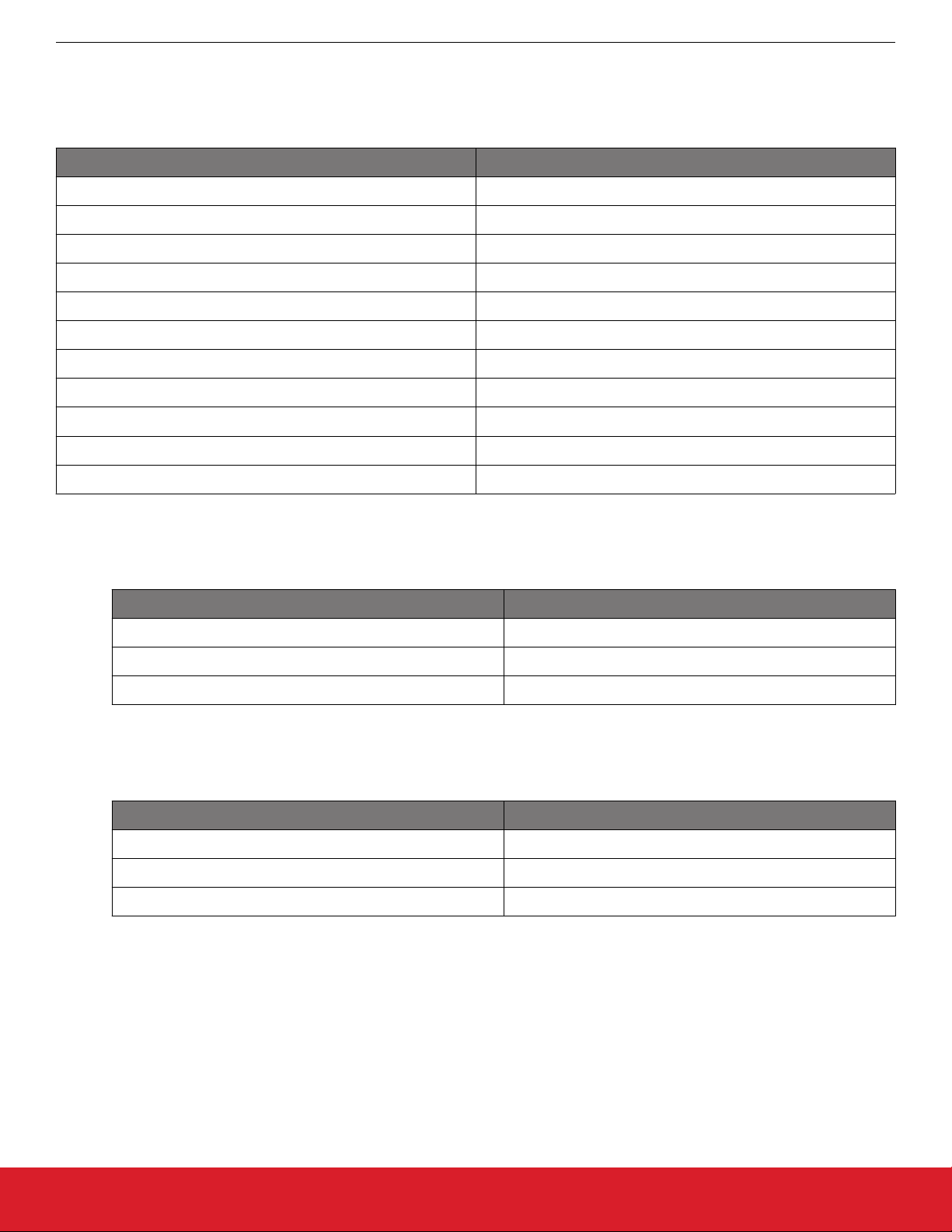
3.3 Fault Monitoring
Si5386 Rev. E Reference Manual
Clock Inputs (IN0, IN1, IN2, IN3)
The four
reference clock is also monitored for LOS since it provides a critical reference clock for the DSPLL. There is also a Loss of Lock (LOL)
indicators asserted when the DSPLL loses synchronization within the feedback loop. The figure below shows the fault monitors for each
input path going into the DSPLL.
input clocks (IN0, IN1, IN2, IN3/FB_IN) are monitored for loss of signal (LOS) and out-of-frequency (OOF). Note that the XAXB
OSC
IN0
IN0b
IN1
IN1b
IN2
IN2b
IN3/FB_IN
IN3b/FB_INb
÷P
÷P
÷P
÷P
Precision
LOS
0
LOS
1
LOS
2
LOS
3
OOF
OOF
OOF
OOF
Fast
Precision
Fast
Precision
Fast
Precision
Fast
LOL
Feedback
Clock
LOS
XAXB
÷M
DSPLL
LPFPD
÷5
Figure 3.2. Si5386 Fault Monitors
3.3.1 Input LOS (Loss-of-Signal) Detection
The loss
the input LOS circuits has its own programmable sensitivity that allows missing edges or intermittent errors to be ignored. LOS sensitivity is configurable using the ClockBuilder Pro utility. The LOS status for each of the monitors is accessible by reading its status register
bit. The live LOS register always displays the current LOS state. Also, there is a sticky flag register which stays asserted until cleared
by the user.
3.3.2 XAXB Reference Clock LOSXAXB (Loss-of-Signal) Detection
A LOS
detected. This feature can be disabled such that the device will continue to produce output clocks even when LOSXAXB is detected.
The table below lists the loss of signal status indicators and fault monitoring control registers.
of signal monitor measures the period of each input clock cycle to detect phase irregularities or missing clock edges. Each of
Monitor
LOS
en
Figure 3.3. LOS Status Indicator
monitor is also available to ensure that the reference clock is valid. By default the output clocks are disabled when LOSXAXB is
Live
LOS
LOS
Sticky
silabs.com | Building a more connected world. Rev. 1.0 | 22
Page 23

Table 3.7. LOS Monitoring and Control Registers
Si5386 Rev. E Reference Manual
Clock Inputs (IN0, IN1, IN2, IN3)
Register Name Hex Address
LOS Status and Controls
LOS 0x000D[3:0] LOS status indicators for IN3 - IN0.
LOS_FLG 0x0012[3:0] LOS indicator sticky flag bits for IN3 - IN0. Remains asser-
LOS_INTR_MSK 0x0018[3:0] Masks LOS from generating INTRb interrupt for IN3 - IN0.
LOS_EN 0x002C[3:0] LOS enable bits for IN3 - IN0. Allows disabling LOS moni-
Function
[Bit Field]
0: Input signal detected or input buffer disabled or LOS disabled
1: Insufficient Input signal detected (LOS)
ted after the indicator bit shows a fault until cleared by the
user. Writing a 0 to the flag bit will clear it if the indicator bit
is no longer asserted.
0: Allow LOS interrupt (default)
1: Mask (ignore) LOS for interrupt
tors on unused inputs.
0: Disable input LOS
1: Enable input LOS
LOS_VAL_TIME 0x002D[7:0] LOS clear validation time for IN3 - IN0. This sets the time
that an input must have a valid clock before the LOS condition is cleared. 0: 2 ms, 1: 100 ms, 2: 200 ms, and 3: 1 s
LOS_TRIG_THR 0x002E[7:0]-0x0035[7:0] Sets the LOS trigger threshold and clear sensitivity for IN3 -
LOS_CLR_THR 0x0036[7:0]-0x003D[7:0]
IN0. These values are determined by ClockBuilder Pro.
LOS_EN 0x002C[3:0] Enable LOS detection on IN3 - IN0. 0: Disable LOS Detec-
tion 1: Enable LOS Detection (default)
LOSXAXB Status and Controls
LOSXAXB 0x000C[1] LOS indicator for the XAXB reference clock
0: Reference clock signal detected
1: Reference clock signal not detected
LOSXAXB_FLG 0x0011[1] LOSXAXB status indicator sticky flag bit. Remains asserted
after the indicator bit shows a fault until cleared by the user.
Writing a 0 to the flag bit will clear it if the indicator bit is no
longer asserted.
LOSXAXB_INTR_MSK 0x0017[1] Masks LOSXAXB from generating INTRb interrupt.
0: Allow LOSXAXB interrupt (default)
1: Mask (ignore) LOSXAXB for interrupt
LOSXAXB_DIS 0x002C[4] Enable LOS detection on the XAXB reference clock.
0: Enable LOS Detection (default).
1: Disable LOS Detection
silabs.com | Building a more connected world. Rev. 1.0 | 23
Page 24
3.3.3 Input OOF (Out-of-Frequency) Detection
Si5386 Rev. E Reference Manual
Clock Inputs (IN0, IN1, IN2, IN3)
Each input
clock is monitored for frequency accuracy with respect to an OOF reference which it considers as its 0 ppm reference. This
OOF reference can be selected as either:
• XAXB reference clock
• IN0, IN1, IN2, IN3
The final OOF status is determined by the combination of both a precise OOF monitor and a fast OOF monitor as shown in the figure
below. An option to disable either monitor is also available. The live OOF register always displays the current OOF state and its sticky
flag register bit stays asserted until cleared. Note that IN3 is only available as an OOF reference when the device is not in ZDM.
Sticky
OOF
Monitor
Precision
en
LOS
OOF
Fast
en
Figure 3.4. OOF Status Indicator
The Precision OOF monitor circuit measures the frequency of all input clocks to within up to ±1 ppm accuracy with respect to the selected OOF frequency reference. A valid input clock frequency is one that remains within the register-programmable OOF frequency range
of up to ±500 ppm in steps of 1/16 ppm. A configurable amount of hysteresis is also available to prevent the OOF status from toggling
at the failure boundary. An example is shown in the figure below. In this case, the OOF monitor is configured with a valid frequency
range of ±6 ppm and with 2 ppm of hysteresis. An option to use one of the input pins (IN0–IN3) as the 0 ppm OOF reference instead of
the XAXB reference clock is available. These options are all register configurable.
Live
OOF Declared
Hysteresis Hysteresis
f
IN
OOF Cleared
-6 ppm -4 ppm 0 ppm +4 ppm +6 ppm
(Clear)(Set)
OOF
(Clear) (Set)
Reference
Figure 3.5. Example of Precision OOF Status Monitor Set and Clear Thresholds
The table below lists the OOF monitoring and control registers. Because the precision OOF monitor needs to provide 1/16 ppm of frequency measurement
accuracy, it must measure the monitored input clock frequencies over a relatively long period of time. However,
this may be too slow to detect an input clock that is quickly ramping in frequency. An additional level of OOF monitoring called the Fast
OOF monitor runs in parallel with the precision OOF monitors to quickly detect a ramping input frequency. The Fast OOF responds
more quickly, and has larger thresholds.
Table 3.8. OOF Status Monitoring and Control Registers
Register Name Hex Address
Function
[Bit Field]
OOF Status and Controls
OOF 0x000D[7:4] OOF status indicators for IN3 - IN0.
0: Input signal detected or input buffer disabled or
OOF disabled
1: Insufficient Input signal detected (OOF)
OOF_FLG 0x0012[7:4] OOF indicator sticky flag bits for IN3 - IN0. Remains
asserted after the indicator bit shows a fault until
cleared by the user. Writing a 0 to the flag bit will
clear it if the indicator bit is no longer asserted.
silabs.com | Building a more connected world. Rev. 1.0 | 24
Page 25

Si5386 Rev. E Reference Manual
Clock Inputs (IN0, IN1, IN2, IN3)
Register Name Hex Address
OOF_INTR_MSK 0x0018[7:4] Masks OOF from generating INTRb interrupt for
Precision OOF Controls
OOF_EN 0x003F[3:0] Enable Precision OOF for IN3 - IN0.
OOF_REF_SEL 0x0040[2:0] Selects clock used for OOF as the 0 ppm refer-
OOF_SET_THR 0x0046[7:0]-0x0049[7:0] OOF Set threshold for IN3 – IN0. Range is up to
OOF_CLR_THR 0x004A[7:0]-0x004D[7:0] OOF Clear threshold for each input. Range is up to
Fast OOF Controls
Function
[Bit Field]
IN3 - IN0.
0: Allow OOF interrupt (default)
1: Mask (ignore) OOF for interrupt
0: Disable Precision OOF
1: Enable Precision OOF
ence. Selections are: XAXB, IN0, IN1, IN2, IN3. Default is XAXB. Note that IN3 may not be used when
the device is in ZDM.
±500 ppm in steps of 1/16 ppm.
±500 ppm in steps of 1/16 ppm.
FAST_OOF_EN 0x003F[7:4] Enable Fast OOF for IN3 - IN0.
0: Disable Precision OOF
1: Enable Precision OOF
FAST_OOF_SET_THR 0x0051[7:0]-0x0054[7:0] Fast OOF Set threshold for IN3 - IN0. Range is
from ±1,000 ppm to ±16,000 ppm in 1000 ppm
steps.
FAST_OOF_CLR_THR 0x0055[7:0]-0x0058[7:0] OOF Clear threshold for each input. Range is from
±1,000 ppm to ±16,000 ppm in 1,000 ppm steps.
silabs.com | Building a more connected world. Rev. 1.0 | 25
Page 26
3.3.4 DSPLL LOL (Loss-of-Lock) Detection and the LOLb Output Indicator Pin
Si5386 Rev. E Reference Manual
Clock Inputs (IN0, IN1, IN2, IN3)
The Loss
is also a dedicated loss of lock pin that reflects the loss of lock condition. The LOL monitor functions by measuring the frequency difference between the input and feedback clocks at the phase detector. There are four parameters to the LOL monitor.
1. Assert to set the LOL.
2. Fast assert to set the LOL.
3. De-assert to clear the LOL.
4. Clear delay.
A block diagram of the LOL monitor is shown in the figure below. The live LOL register always displays the current LOL state and a
sticky register always stays asserted until cleared. The LOLb pin reflects the current state of the LOL monitor.
of Lock (LOL) monitor asserts a LOL register bit when the DSPLL has lost synchronization with its selected input clock. There
a. User sets the threshold in ppm in CBPro.
a. CBPro sets this to ~100 times the assert threshold.
b. A very large ppm error in a short time will assert the LOL.
a. User sets the threshold in ppm in CBPro.
a. CBPro sets this based upon the project plan.
LOL Monitor
LOL
Clear
Timer
LOS
LOL
Sticky
LOL
Set
Live
LOLb
DSPLL
f
IN
LPFPD
Feedback
Clock
÷M
The LOL frequency monitor has an adjustable sensitivity which is register-configurable from ±1 ppm to ±10,000 ppm. Having two separate frequency monitors allows for hysteresis to help prevent chattering of LOL status. An example configuration where LOCK is indicated when there is less than 0.1 ppm frequency difference at the inputs of the phase detector and LOL is indicated when there's more
than 10 ppm frequency difference is shown in the figure below.
LOL Declared
Locked
Loss of
Lock
-10 ppm -0.1 ppm
÷5
Figure 3.6. Si5386 LOL Status Indicator
Lock
Acquisition
Hysteresis Hysteresis
0 ppm
(Clear)(Set)
Phase Detector Frequency Difference
+0.1 ppm +10 ppm
(Clear) (Set)
Loss of
Lock
f
DIFF
Figure 3.7. Example of LOL Set and Clear Thresholds
A timer delays clearing of the LOL indicator to allow additional time for the DSPLL to completely lock to the inpujt clock. The timer is
also useful to prevent the LOL indicator from toggling or chattering as the DSPLL completes lock acquisition. The configurable delay
value depends on frequency configuration and loop bandwidth of the DSPLL and is automatically calculated using the ClockBuilder Pro
utility. It is important to know that, in addition to being a status bit, LOL automatically enables Fastlock by default.
silabs.com | Building a more connected world. Rev. 1.0 | 26
Page 27

Table 3.9. LOL Status Monitor and Control Registers
Si5386 Rev. E Reference Manual
Clock Inputs (IN0, IN1, IN2, IN3)
Register Name Hex Address
Function
[Bit Field]
LOL 0x000E[1] LOL status indicator for the DSPLL.
0: DSPLL Locked to input clock
1: DSPLL Not locked to an input clock
LOL_FLG 0x0013[1] LOL indicator sticky flag bit. Remains as-
serted after the indicator bit shows a fault
until cleared by the user. Writing a 0 to the
flag bit will clear it if the indicator bit is no
longer asserted.
LOL_INTR_MSK 0x0019[1] Masks LOL from generating INTRb inter-
rupt.
0: Allow LOL interrupt (default)
1: Mask (ignore) LOL for interrupt
LOL_SLW_SET_THR 0x009E[7:4] Configures the loss of lock set thresholds.
Selectable as
1,3,10,30,100,300,1000,3000,10000. Values are in ppm.
LOL_SLW_CLR_THR 0x00A0[7:4] Configures the loss of lock set thresholds.
Selectable as
0.1,0.3,1,3,10,30,100,300,1000,3000,1000
0. Values are in ppm.
LOL_CLR_DELAY_DIV256 0x00A9[7:0]-0x00AC[4:0] This is a 29-bit register that configures the
delay value for the LOL Clear delay. This
value depends on the DSPLL frequency
configuration and loop bandwidth. It is calculated using the ClockBuilder Pro utility.
LOL_TIMER_EN 0x00A2[1] Enable for the LOL Clear Timer.
0: Disable LOL clear timer
1: Enable LOL clear timer
LOL_FST_EN 0x0092[1] Fast LOL Enable. Large input frequency er-
rors will quickly assert LOL when enabled.
0: Disable Fast LOL
1: Enable Fast LOL (default)
The settings in the above table are handled by ClockBuilder Pro. Manual settings should be avoided.
silabs.com | Building a more connected world. Rev. 1.0 | 27
Page 28

3.3.5 Device Status Monitoring
Si5386 Rev. E Reference Manual
Clock Inputs (IN0, IN1, IN2, IN3)
In addition
to the input-driven LOS, LOSXAXB, OOF, LOL, and HOLD fault monitors discussed previously, there are several additional
status monitors which may be useful in determining the device operating state. While some of these indicators may seem redundant,
they are either taken from different locations in the device or are active in different operating modes. These indicators can provide further insight into the operating state of the device.
Table 3.10. Device Status Monitoring and Control Registers
Register Name
Hex Address
[Bit Field]
Function
Device in Calibration status indicator.
SYSINCAL 0x000C[0]
0: Normal Operation
1: Device in Calibration
LOS status indicator for XAXB reference
clock.
LOSREF 0x000C[2]
0: Reference clock signal detected
1: Insufficient reference clock signal detected
XAXB reference clock locking status indicator.
XAXB_ERR 0x000C[3]
0: Locked to reference clock
SMBUS_TMOUT 0x000C[5]
CAL 0x000F[5]
SYSINCAL_FLG 0x0011[0]
LOSREF_FLG 0x0011[2]
XAXB_ERR_FLG 0x0011[3]
1: Not locked to reference clock
SMB Bus Timeout Indicator.
0: SMB Bus Timeout has Not occurred
1: SMB Bus Timeout Has occurred
DSPLL in Calibration status indicator.
0: Normal Operation
1: DSPLL in Calibration
SYSINCAL indicator sticky flag bit. Remains asserted after the indicator bit shows
a fault until cleared by the user. Writing a 0
to the flag bit will clear it if the indicator bit
is no longer asserted.
LOSREF indicator sticky flag bit. Remains
asserted after the indicator bit shows a fault
until cleared by the user. Writing a 0 to the
flag bit will clear it if the indicator bit is no
longer asserted.
XAXB_ERR indicator sticky flag bit. Remains asserted after the indicator bit shows
a fault until cleared by the user. Writing a 0
to the flag bit will clear it if the indicator bit
is no longer asserted.
SMBUS_TMOUT indicator sticky flag bit.
Remains asserted after the indicator bit
SMBUS_TMOUT_FLG 0x0011[5]
shows a fault until cleared by the user.
Writing a 0 to the flag bit will clear it if the
indicator bit is no longer asserted.
silabs.com | Building a more connected world. Rev. 1.0 | 28
Page 29
Si5386 Rev. E Reference Manual
Clock Inputs (IN0, IN1, IN2, IN3)
Register Name
CAL_FLG 0x0014[5]
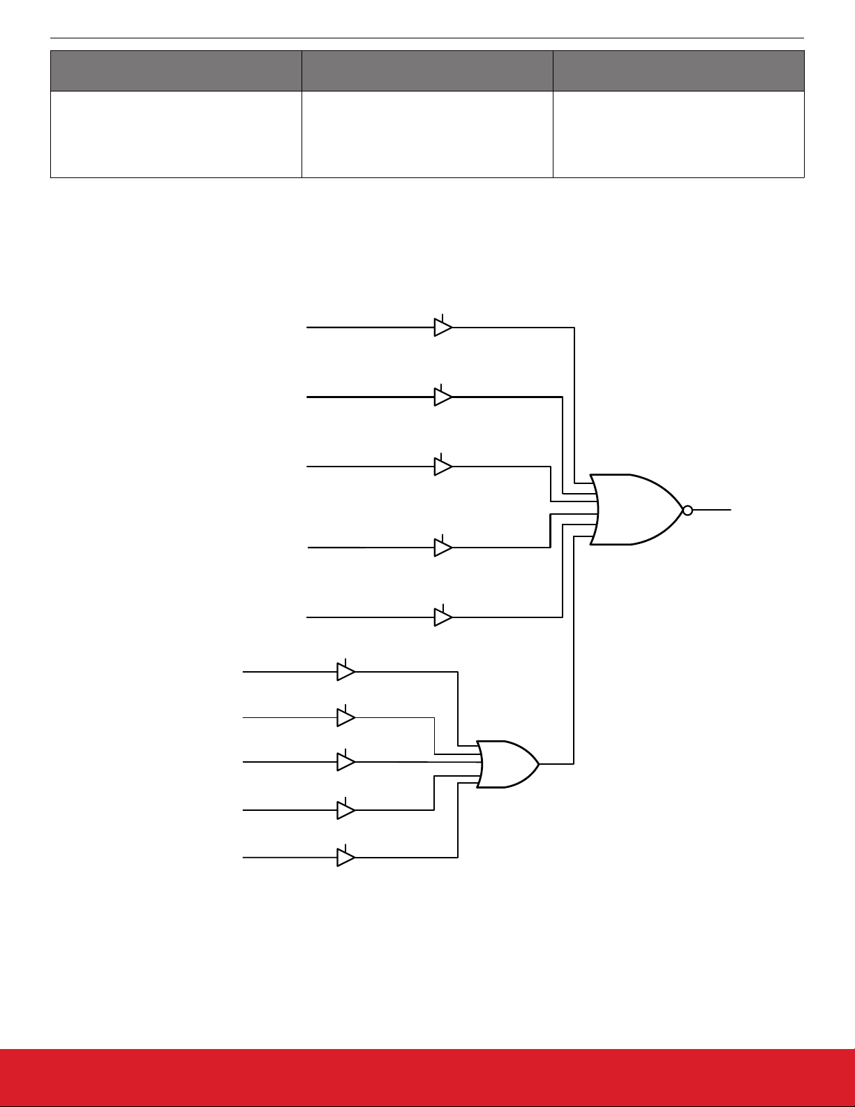
3.3.6 INTRb Interrupt Configuration
The INTRb
polling may also be used to monitor device status. Each of the status indicator flags is maskable to avoid unwanted assertion of the
interrupt pin. The state of the INTRb pin is reset by clearing the unmasked status flag register bit(s) that caused the interrupt. Note that
the status flag register bits cannot be cleared if the corresponding status indicator is still showing a fault.
interrupt output pin is a convenient way to monitor a change in state of one or more status indicator flags, though direct
Hex Address
[Bit Field]
LOS_INTR_MSK[3-0]
Function
CAL indicator sticky flag bit. Remains asserted after the indicator bit shows a fault
until cleared by the user. Writing a 0 to the
flag bit will clear it if the indicator bit is no
longer asserted.
LOS_FLG[3-0]
OOF_INTR_MSK[3-0]
OOF_FLG[3-0]
LOL_INTR_MSK
LOL_FLG
HOLD_FLG
SYSINCAL_FLG
LOSXAXB_FLG
LOSREF_FLG
XAXB_ERR_FLG
SMB_TMOUT_FLG
HOLD_INTR_MSK
INTRb
CAL_INTR_MSK
CAL_FLG
SYSINCAL_INTR_MSK
LOSXAXB_INTR_MSK
LOSREF_INTR_MSK
XAXB_ERR_INTR_MSK
SMB_TMOUT_INTR_MSK
Figure 3.8. Interrupt Pin Source Masking Options
silabs.com | Building a more connected world. Rev. 1.0 | 29
Page 30

Table 3.11. INTRb Pin Interrupt Mask Registers
Si5386 Rev. E Reference Manual
Clock Inputs (IN0, IN1, IN2, IN3)
Register Name Hex Address
Function
[Bit Field]
LOS_INTR_MSK 0x0018[3:0] Masks LOS from generating INTRb interrupt for IN3 - IN0.
0: Allow LOS interrupt (default)
1: Mask (ignore) LOS for interrupt
OOF_INTR_MSK 0x0018[7:4] Masks OOF from generating INTRb interrupt for IN3 - IN0.
0: Allow OOF interrupt (default)
1: Mask (ignore) OOF for interrupt
LOL_INTR_MSK 0x0019[1] Masks LOL from generating INTRb interrupt.
0: Allow LOL interrupt (default)
1: Mask (ignore) LOL for interrupt
HOLD_INTR_MSK 0x0019[5] Masks Holdover/Freerun from generating INTRb interrupt.
0: Allow Holdover/Freerun interrupt (default)
1: Mask (ignore) Holdover/Freerun for interrupt
CAL_INTR_MSK 0x001A[5] Masks CAL from generating INTRb interrupt.
0: Allow CAL interrupt (default)
1: Mask (ignore) CAL for interrupt
SYSINCAL_INTR_MSK 0x0017[0] Masks SYSINCAL from generating INTRb interrupt.
0: Allow SYSINCAL interrupt (default)
1: Mask (ignore) SYSINCAL for interrupt
LOSXAXB_INTR_MSK 0x0017[1] Masks LOSXAXB from generating INTRb interrupt.
0: Allow LOSXAXB interrupt (default)
1: Mask (ignore) LOSXAXB for interrupt
LOSREF_INTR_MSK 0x0017[2] Masks LOSREF from generating INTRb interrupt.
0: Allow LOSREF interrupt (default)
1: Mask (ignore) LOSREF for interrupt
XAXB_ERR_INTR_MSK 0x0017[3] Masks XAXB_ERR from generating INTRb interrupt.
0: Allow XAXB_ERR interrupt (default)
1: Mask (ignore) XAXB_ERR for interrupt
SMB_TMOUT_INTR_MSK 0x0017[5] Masks SMB_TMOUT from generating INTRb interrupt.
0: Allow SMB_TMOUT interrupt (default)
1: Mask (ignore) SMB_TMOUT for interrupt
silabs.com | Building a more connected world. Rev. 1.0 | 30
Page 31

Si5386 Rev. E Reference Manual
Output Clocks
4. Output Clocks
Each output driver has configurable output amplitude and common mode voltage, covering a wide variety of differential signal output
formats including LVPECL, LVDS, HCSL, and CML. In addition to supporting differential signals, any of the outputs can be configured
as single-ended LVCMOS (3.3, 2.5, or 1.8V) providing up to 20 single-ended outputs or any combination of differential and singleended outputs. Unused outputs may be left unconnected.
4.1 Output Crosspoint Switch
A crosspoint switch allows any of the output drivers to connect with any of the Output N dividers as shown in the figure below. The
crosspoint configuration is programmable and can be stored in NVM so that the desired output configuration is ready at power up. Any
N divider can source multiple, or even all, output drivers.
VDDO0
÷N
÷N
÷N
÷N
÷N
÷R
0A
÷R
0
0
÷R
÷R
÷R
÷R
÷R
÷R
1
2
3
4
5
6
1
2
3
4
OUT0A
OUT0Ab
OUT0
OUT0b
VDDO1
OUT1
OUT1b
VDDO2
OUT2
OUT2b
VDDO3
OUT3
OUT3b
VDDO4
OUT4
OUT4b
VDDO5
OUT5
OUT5b
VDDO6
OUT6
OUT6b
VDDO7
÷R
7
÷R
8
÷R
9
÷R
9A
Figure 4.1. N Divider to Output Driver Crosspoint
The following table is used to set up the routing from the N divider frequency selection to the output.
silabs.com | Building a more connected world. Rev. 1.0 | 31
OUT7
OUT7b
VDDO8
OUT8
OUT8b
OUT9
OUT9b
OUT9A
OUT9Ab
VDDO9
Page 32

Table 4.1. Output Crosspoint Configuration Registers
Si5386 Rev. E Reference Manual
Output Clocks
Register Name Hex Address
OUT0A_MUX_SEL 0x0106[2:0] Connects the output drivers to one of the N
OUT0_MUX_SEL 0x010B[2:0]
OUT1_MUX_SEL 0x0110[2:0]
OUT2_MUX_SEL 0x0115[2:0]
OUT3_MUX_SEL 0x011A[2:0]
OUT4_MUX_SEL 0x011F[2:0]
OUT5_MUX_SEL 0x0124[2:0]
OUT6_MUX_SEL 0x0129[2:0]
OUT7_MUX_SEL 0x012E[2:0]
OUT8_MUX_SEL 0x0133[2:0]
OUT9_MUX_SEL 0x0138[2:0]
OUT9A_MUX_SEL 0x013D[2:0]
4.1.1 Output R Divider Synchronization
Function
[Bit Field]
divider sources. Selections are:
0: N0
1: N1
2: N2
3: N3
4: N4
5-7: Reserved
All the
output R dividers are reset to a known state during the power-up initialization period. This ensures consistent and repeatable
output phase alignment. Resetting the device using the RSTb pin or asserting the Hard Reset bit 0x001E[1] will give the same result.
Also, the output R dividers can be reset by driving the SYNCb input pin low or by setting the SYNC register bit (0x001E[2]) high. Soft
Reset does not affect the output synchronization.
silabs.com | Building a more connected world. Rev. 1.0 | 32
Page 33

4.2 Performance Guidelines for Outputs
Si5386 Rev. E Reference Manual
Output Clocks
Whenever a
number of high frequency, fast rise time, large amplitude signals are located close to one another, the laws of physics
dictate that there will be some amount of crosstalk. Use of integer-related output frequencies reduces the opportunity for crosstalk as
these frequencies are derived from the same output divider. However, the phase noise of the Si5386 is so low that crosstalk may still be
detected in certain cases. Crosstalk occurs at both the device level, as well as the PCB level. It is difficult (and possibly irrelevant) to
allocate the crosstalk contributions between these two sources since it can only be measured, while the Si5386 is mounted on a PCB.
In addition to following the PCB layout guidelines given in 9. XO and Device Circuit Layout Recommendations, crosstalk can be minimized by modifying the placements of the different output clock frequencies. For example, consider the following lineups of output
clocks in the table below. The “Clock Placement Wizard ...” button on the “Define Output Frequencies” page of ClockBuilder Pro provides an easy way to change the frequency placements by either Manual or Automatic means.
Table 4.2. Comparison of Output Clock Frequency Placement Choices
Output Not Recommended (Frequency MHz) Recommended (Frequency MHz)
0A — 155.52
0 — —
1 100 100
2 155.52 125
3 156.25 156.25
4 122.88 —
5 125 —
6 245.76 983.04
7 983.04 491.52
8 491.52 245.76
9 — 122.98
9A — —
Using this example, a few guidelines are illustrated:
1. Avoid adjacent
frequency values that are close in frequency. A 156.25 MHz clock should not be placed next to a 155.52 MHz clock
as crosstalk will be observed at 0.73 MHz offset from each frequency. If the jitter integration bandwidth or spur range goes up to 20
MHz then keep adjacent frequencies at least 20 MHz apart.
2. Frequency values that are integer multiples of one another should be grouped together. Noting that 983.04 MHz = 2 x 491.52 MHz
= 4 x 245.76 MHz = 8 x 122.88 MHz, it is okay to place each of these frequency values next to one another.
3. Unused outputs can also be placed to separate clock outputs that might otherwise show crosstalk.
4. If some outputs have tighter spur requirements while others are relatively loose, rearrange the clock outputs so that the critical
outputs are the least susceptible to crosstalk.
5. Because CMOS outputs have large pk-pk swings, are single ended, and do not present a balanced load to the VDDO supplies,
CMOS outputs generate much more crosstalk than differential outputs. For this reason, CMOS outputs should be avoided whenever possible. When CMOS is unavoidable, even greater care must be taken with respect to the above guidelines. For more information on these issues, see AN862: Optimizing Si534x Jitter Performance in Next Generation Internet Infrastructure Systems.
silabs.com | Building a more connected world. Rev. 1.0 | 33
Page 34

4.2.1 Optimizing Output Phase Noise
Si5386 Rev. E Reference Manual
Output Clocks
To obtain
the best phase noise performance for RF and other demanding applications, it is important to configure the Si5386 device
optimally. Using integer dividers for P, M, and N will provide the highest level of performance. Integer mode dividers are optimized to
support LTE, JESD204b and other integer-ratio derived frequencies.
Tips for optimizing phase noise performance, with suggestions listed most important to least important:
1. Use an Integer-N output divider. This requires the output frequency to be an even integer divisor from the VCO frequency.
2. Use Integer-P input dividers.
3. Use Integer-M feedback divider. In many cases fractional M performance is indistinguishable from integer performance. However, it
is possible that there may be some cases where this can measurably increase phase noise.
4. Follow the crosstalk guidelines given above in all cases. Where possible, leave an unused output between all-integer outputs and
outputs using fractional N output dividers. ClockBuilder Pro provides a means for manually choosing DSPLL N dividers for each
output on the "Define Output Frequencies" page. Also, the "Clock Placement Wizard" allows for manual or automatic output placement to reduce the likelihood of crosstalk.
4.3 Output Signal Format
The differential output amplitude and common mode voltage are both fully programmable covering a wide variety of signal formats including LVDS, LVPECL, HCSL. For CML applications, see 13. Appendix—Custom Differential Amplitude Controls. The standard formats can be either Normal or Low-Power. Low-Power format uses less power for the same amplitude but has the drawback of slower
rise/fall times. The source impedance in the Low-Power format is higher than 100 Ω. See 13. Appendix—Custom Differential Amplitude
Controls for register settings to implement variable amplitude differential outputs. In addition to supporting differential signals, any of the
outputs can be configured as LVCMOS (3.3, 2.5, or 1.8 V) drivers providing up to 20 single-ended outputs, or any combination of differential and single-ended outputs. Note also that CMOS output can create much more crosstalk than differential outputs so extra care
must be taken in their pin replacement so that other clocks that need best spur performance are not on nearby pins. See AN862: Opti-
mizing Si534x Jitter Performance in Next Generation Internet Infrastructure Systems. Note that options 5 & 6 allow for only a single
output pin to be active with LVCMOS signals. This reduces power consumption and crosstalk from noisy CMOS signals to other clocks.
Also note that output frequencies > 1474.56 MHz are restricted to Normal Differential format and that only 2.5 V and 3.3 V options are
allowed.
Table 4.3. Output Signal Format Registers
Register Name Hex Address
Function
[Bit Field]
OUT0A_FORMAT 0x0104[2:0] Selects the output signal format as differen-
OUT0_FORMAT 0x0109[2:0]
OUT1_ FORMAT 0x010E[2:0]
OUT2_ FORMAT 0x0113[2:0]
OUT3_ FORMAT 0x0118[2:0]
OUT4_ FORMAT 0x011D[2:0]
OUT5_ FORMAT 0x0122[2:0]
OUT6_ FORMAT 0x0127[2:0]
OUT7_ FORMAT 0x012C[2:0]
OUT8_ FORMAT 0x0131[2:0]
tial or LVCMOS mode.
0: Reserved
1: Normal Differential
2: Low-Power Differential
3: Reserved
4: LVCMOS
5: LVCMOS (OUTx pin only)
6: LVCMOS (OUTxb pin only)
7: Reserved
OUT9_ FORMAT 0x0136[2:0]
OUT9A_FORMAT 0x013B[2:0]
silabs.com | Building a more connected world. Rev. 1.0 | 34
Page 35

4.4 Output Driver Supply Select
Si5386 Rev. E Reference Manual
Output Clocks
The VDDO
output driver voltage may be selected separately for each driver. The selected voltage must match the voltage supplied to
that VDDO pin in the end system. VDDO pins for unused (unconnected) outputs can be left unconnected, or may be connected to a
convenient 1.8 V–3.3 V system supply without increasing power dissipation.
Table 4.4. Output Driver Supply Select
Hex Address
Register Name
Function
[Bit Field]
Output Driver VDD Select Enable.
OUT0A_VDD_SEL_EN 0x0106[3]
Set to 1 for normal operation.
Output Driver VDD Select
0: 1.8 V
OUT0A_VDD_SEL 0x0106[5:4]
1: 2.5 V
2: 3.3 V
3: Reserved
OUT0_VDD_SEL_EN 0x010B[3]
OUT0_VDD_SEL 0x010B[5:4]
OUT1_VDD_SEL_EN 0x0110[3]
OUT1_VDD_SEL 0x0110[5:4]
OUT2_VDD_SEL_EN 0x0115[3]
OUT2_VDD_SEL 0x0115[5:4]
OUT3_VDD_SEL_EN 0x011A[3]
OUT3_VDD_SEL 0x011A[5:4]
OUT4_VDD_SEL_EN 0x011F[3]
OUT4_VDD_SEL 0x011F[5:4]
OUT5_VDD_SEL_EN 0x0124[3]
OUT5_VDD_SEL 0x0124[5:4]
OUT6_VDD_SEL_EN 0x0129[3]
OUT6_VDD_SEL 0x0129[5:4]
OUT7_VDD_SEL_EN 0x012E[3]
OUT7_VDD_SEL 0x012E[5:4]
OUT8_VDD_SEL_EN 0x0133[3]
OUT8_VDD_SEL 0x0133[5:4]
OUT9_VDD_SEL_EN 0x0138[3]
Similar to OUT0A settings
OUT9_VDD_SEL 0x0138[5:4]
OUT9A_VDD_SEL_EN 0x013D[3]
OUT9A_VDD_SEL 0x013D[5:4]
silabs.com | Building a more connected world. Rev. 1.0 | 35
Page 36

4.5 Differential Outputs
4.5.1 Differential Output Terminations
The differential output drivers support both ac and dc-coupled terminations as shown in the following figure.
Si5386 Rev. E Reference Manual
Output Clocks
V
DDO
= 3.3V, 2.5V , 1.8V
V
DDO
V
= 3. 3V, 2.5V , 1.8V
DDO
DC Coupled LVDS
= 3.3 V, 2.5V
OUTx
OUTxb
50
50
DC Coupled LVCMOS
OUTx
OUTxb
Rs
Rs
AC Coupled HCSL
AC Coupled LVDS/LVPECL
V
= 3. 3V, 2.5V , 1.8V
DDO
50
100
50
Internally
self-biased
100
OUTx
OUTxb
AC Coupled LVPECL/CML
3.3V , 2.5V , 1.8 V
LVCMOS
50
50
VDD
RX
R1
R1
V
DDO
= 3. 3V, 2.5V
OUTx
OUTxb
50
50
VDD – 1.3V
5050
OUTx
OUTxb
For VCM= 0.35V
VDD
RX
3.3V
2.5V
1.8V
50
50
50
R2
R2
Standard
HCSL
Receiver
R1 R2
442
332
243
56. 2
59
63. 4
Figure 4.2. Si5386 Supported Differential Output Terminations
silabs.com | Building a more connected world. Rev. 1.0 | 36
Page 37

4.5.2 Differential Output Amplitude Controls
Si5386 Rev. E Reference Manual
Output Clocks
The differential
amplitude of each output can be controlled with the following registers. See 4.5.4 Recommended Settings for Differen-
tial LVPECL, LVDS, HCSL, and CML for recommended OUTx_AMPL settings for common signal formats. See 4.5.2 Differential Output
Amplitude Controls for register settings for non-standard amplitudes.
Table 4.5. Differential Output Voltage Swing Registers
Register Name Hex Address
Function
[Bit Field]
OUT0A_AMPL 0x0105[6:4] Sets the voltage swing for the differential
OUT0_AMPL 0x010A[6:4]
OUT1_ AMPL 0x010F[6:4]
output drivers for both Normal and LowPower modes. This field only applies when
OUTx_FORMAT = 1 or 2.
OUT2_ AMPL 0x0114[6:4]
OUT3_ AMPL 0x0119[6:4]
OUT4_ AMPL 0x011E[6:4]
OUT5_ AMPL 0x0123[6:4]
OUT6_ AMPL 0x0128[6:4]
OUT7_ AMPL 0x012D[6:4]
OUT8_ AMPL 0x0132[6:4]
OUT9_ AMPL 0x0137[6:4]
OUT9A_ AMPL 0x013C[6:4]
4.5.3 Differential Output Common Mode Voltage Selection
The common
mode voltage (VCM) for differential output Normal and Low-Power modes is selectable depending on the supply voltage
provided at the output’s VDDO pin. See the table below for recommended OUTx_CM settings for common signal formats. See
13. Appendix—Custom Differential Amplitude Controls " for recommended OUTx_CM settings when using custom output amplitude.
Table 4.6. Differential Output Common Mode Voltage Selection Registers
Register Name Hex Address
Function
[Bit Field]
OUT0A_CM 0x0105[3:0] Sets the common mode voltage for the dif-
OUT0_CM 0x010A[3:0]
ferential output driver. This field only applies when OUTx_FORMAT = 1 or 2.
OUT1_ CM 0x010F[3:0]
OUT2_ CM 0x0114[3:0]
OUT3_ CM 0x0119[3:0]
OUT4_ CM 0x011E[3:0]
OUT5_ CM 0x0123[3:0]
OUT6_ CM 0x0128[3:0]
OUT7_ CM 0x012D[3:0]
OUT8_ CM 0x0132[3:0]
OUT9_ CM 0x0137[3:0]
OUT9A_ CM 0x013C[3:0]
silabs.com | Building a more connected world. Rev. 1.0 | 37
Page 38

Si5386 Rev. E Reference Manual
Output Clocks
4.5.4 Recommended Settings for Differential LVPECL, LVDS, HCSL, and CML
Each differential output has four settings for control:
1. Normal or Low-Power Format
Amplitude (sometimes called Swing)
2.
3. Common Mode Voltage
4. Stop High or Stop Low (See 4.7.1 Output Driver State When Disabled for details.)
The Normal mode setting includes an internal 100 Ω resistor between the OUT and OUTb pins. In Low-Power mode, this resistor is
removed, resulting in a higher output impedance. The increased impedance creates larger amplitudes for the same power while reducing edge rates, which may increase jitter or phase noise. In either mode, the differential receiver must be properly terminated to the
PCB trace impedance for good system signal integrity. Note that ClockBuilder Pro does not provide Low-Power mode settings. Contact
Silicon Labs Technical Support for assistance with Low-Power mode use.
Amplitude controls are as described in the previous section and also in more detail in 13. Appendix—Custom Differential Amplitude
Controls ". Common mode voltage selection is also described in more detail in this appendix.
Table 4.7. Recommended Settings for Differential LVPECL, LVDS, HCSL, and CML
Standard VDDO Mode OUTx_FORMAT OUTx_CM OUTx_AMPL
(V) (Dec) (Dec) (Dec)
LVPECL 3.3 Normal 1 11 6
LVPECL 2.5 Normal 1 11 6
LVPECL 3.3 Low-Power 2 11 3
LVPECL 2.5 Low-Power 2 11 3
LVDS 3.3 Normal 1 3 3
LVDS 2.5 Normal 1 11 3
Sub-LVDS
1
1.8 Normal 1 13 3
LVDS 3.3 Low-Power 2 3 1
LVDS 2.5 Low-Power 2 11 1
Sub-LVDS
2
HCSL
2
HCSL
2
HCSL
1
1.8 Low-Power 2 13 1
3.3 Low-Power 2 11 3
2.5 Low-Power 2 11 3
1.8 Low-Power 2 13 3
Note:
1. The Sub-LVDS common mode voltage is not compliant with LVDS standards. Therefore, AC coupling the driver to an LVDS receiver is highly recommended in this case.
Creates HCSL compatible signals, see HCSL receiver biasing network in Figure 4.2 Si5386 Supported Differential Output Termi-
2.
nations on page 36.
The output differential driver can also produce a wide range of CML compatible output amplitudes. See 13. Appendix—Custom
Differ-
ential Amplitude Controls for additional information.
4.6 LVCMOS Outputs
silabs.com | Building a more connected world. Rev. 1.0 | 38
Page 39

4.6.1 LVCMOS Output Terminations
LVCMOS outputs are dc-coupled as shown in the following figure.
DC Coupled LVCMOS
V
DDO
= 3.3V
, 1.8V
, 2.5V
OUTx
OUTxb
Rs
Rs
Figure 4.3. LVCMOS Output Terminations
Si5386 Rev. E Reference Manual
Output Clocks
3.3V, 2.5V, 1.8V
LVCMOS
50
50
silabs.com | Building a more connected world. Rev. 1.0 | 39
Page 40

4.6.2 LVCMOS Output Impedance and Drive Strength Selection
Si5386 Rev. E Reference Manual
Output Clocks
Each LVCMOS
driver has a configurable output impedance to accommodate different trace impedances and drive strengths. A series
source termination resistor (Rs) is recommended close to the output to match the selected output impedance to the trace impedance
(i.e. Rs = Trace Impedance – Zs). There are multiple programmable output impedance selections for each VDDO option as shown in
the following table. Generally, the lowest impedance for a given supply voltage is preferable, since it will give the fastest edge rates.
Table 4.8. LVCMOS Output Impedance and Drive Strength Selections
VDDO OUTx_CMOS_DRV Driver Impedance (Zs) Drive Strength (Iol/Ioh)
0x1 38 Ω 10 mA
3.3 V
0x2 30 Ω 12 mA
0x3
1
22 Ω 17 mA
0x1 43 Ω 6 mA
2.5 V
1.8 V
0x2 35 Ω 8 mA
0x3
0x3
1
1
24 Ω 11 mA
31 Ω 5 mA
Note:
1.
Use of the lowest impedance setting is recommended for all supply voltages.
Table 4.9. LVCMOS Drive Strength Registers
Register Name
OUT0A_CMOS_DRV 0x0104[7:6]
OUT0_CMOS_DRV 0x0109[7:6]
OUT1_ CMOS_DRV 0x010E[7:6]
OUT2_ CMOS_DRV 0x0113[7:6]
OUT3_ CMOS_DRV 0x0118[7:6]
OUT4_ CMOS_DRV 0x011D[7:6]
OUT5_ CMOS_DRV 0x0122[7:6]
OUT6_ CMOS_DRV 0x0127[7:6]
OUT7_ CMOS_DRV 0x012C[7:6]
OUT8_ CMOS_DRV 0x0131[7:6]
OUT9_ CMOS_DRV 0x0136[7:6]
OUT9A_ CMOS_DRV 0x013B[7:6]
4.6.3 LVCMOS Output Signal Swing
Hex Address
Function
[Bit Field]
LVCMOS output impedance. See the table
above for settings.
The signal
swing (VOL/VOH) of the LVCMOS output drivers is set by the voltage on the VDDO pins. Each output driver has its own
VDDO pin allowing a unique output voltage swing for each of the LVCMOS drivers. Each output driver automatically detects the voltage
on the VDDO pin to properly determine the correct output voltage.
silabs.com | Building a more connected world. Rev. 1.0 | 40
Page 41

4.6.4 LVCMOS Output Polarity
Si5386 Rev. E Reference Manual
Output Clocks
When a
driver is configured as an LVCMOS output it generates a clock signal on both pins (OUT and OUTb). By default the clock on
the OUTb pin is generated with the same polarity (in phase) with the clock on the OUT pin. The polarity of these clocks is configurable
enabling complimentary clock generation and/or inverted polarity with respect to other output drivers. Note that these settings have no
effect on the differential-mode output driver.
Table 4.10. LVCMOS Output Polarity Registers
Register Name Hex Address
Function
[Bit Field]
OUT0A_INV 0x0106[7:6] Controls the output polarity of the OUT and
OUT0_INV 0x010B[7:6]
OUT pins when in LVCMOS mode. Selections are shown below in the table below.
OUT1_INV 0x0110[7:6]
OUT2_INV 0x0115[7:6]
OUT3_INV 0x011A[7:6]
OUT4_INV 0x011F[7:6]
OUT5_INV 0x0124[7:6]
OUT6_INV 0x0129[7:6]
OUT7_INV 0x012E[7:6]
OUT8_INV 0x0133[7:6]
OUT9_INV 0x0138[7:6]
OUT9A_INV 0x013D[7:6]
Table 4.11. LVCMOS Output Polarity of OUT and OUTb Pins
OUTx_INV
OUT OUTb Comment
Register Settings
0x00 CLK CLK Both in phase (default)
0x01 CLK CLKb Complementary
0x02 CLKb CLKb Both Inverted
0x03 CLKb CLK Inverted Complementary
silabs.com | Building a more connected world. Rev. 1.0 | 41
Page 42

Si5386 Rev. E Reference Manual
Output Clocks
4.7 Output Enable/Disable
Each output driver may be individually placed in one of three operating states:
• “Enabled” state
will be generated, if selected by the output format.
• “Disabled” state gates off clock operation and places the output into a static, user-selectable, logic state. Differential output common
mode voltage is maintained, if selected by the output format, allowing a quick transition back to Enabled state operation with minimal
common mode disruption.
• “Powerdown” state removes power from the output driver and leaves the output pins high-impedance. In this state, regardless of
output format, the output common mode voltage is not generated and the output pin voltages are not well defined. Powerdown is
recommended for unused outputs as well as startup or long-term power reduction, where differential common voltage generation
restart will not introduce issues in the system. For lowest noise during operation, unused LVCMOS output pins should be AC terminated to ground with 50 Ω. See 10.1 Power Management Features for more information on powerdown.
The OEb pin provides a convenient method of enabling or disabling all of the output drivers at the same time. Holding the OEb pin low
enables all of the outputs, while driving it high disables all outputs. In addition to pin control, flexible register controls described in the
following sections allow further customization for each application. Note that any one disable control can disable the corresponding output(s) even if all other sources controls are enabled. See the sections below, especially 4.7.5 Output Driver Disable Source Summary,
for more information on manual and automatic disable controls.
is the normal state for output clock operation. The output clock is toggling and the differential common mode voltage
Table 4.12. Output Enable/Disable Manual Control Registers
Register Name Hex Address
Function
[Bit Field]
OUTALL_DISABLE_LOW 0x0102[0] Enable/Disable all output drivers. If the
OEb pin is held high, then all outputs will
be disabled regardless of the state of this
or the OUTx_OE register bits.
0: Disable All outputs (default)
1: Enable All outputs
OUT0A_OE 0x0103[1] Enable/Disable individual outputs. Note
OUT0_OE 0x0108[1]
OUT1_OE 0x010D[1]
OUT2_OE 0x0112[1]
OUT3_OE 0x0117[1]
that the OEb pin must be held low and
OUTALL_DISABLE_LOW = 1 in order to
enable an output.
0: Disable Output (default)
1: Enable Output
OUT4_OE 0x011C[1]
OUT5_OE 0x0121[1]
OUT6_OE 0x0126[1]
OUT7_OE 0x012B[1]
OUT8_OE 0x0130[1]
OUT9_OE 0x0135[1]
OUT9A_OE 0x013A[1]
silabs.com | Building a more connected world. Rev. 1.0 | 42
Page 43

4.7.1 Output Driver State When Disabled
The disabled state of an output driver is configurable as: disable logic low or disable logic high.
Table 4.13. Output Driver Disable State Registers
Si5386 Rev. E Reference Manual
Output Clocks
Register Name Hex Address
OUT0A_DIS_STATE 0x0104[5:4] Determines the static state of an output
OUT0_DIS_STATE 0x0109[5:4]
OUT1_ DIS_STATE 0x010E[5:4]
OUT2_ DIS_STATE 0x0113[5:4]
OUT3_ DIS_STATE 0x0118[5:4]
OUT4_ DIS_STATE 0x011D[5:4]
OUT5_ DIS_STATE 0x0122[5:4]
OUT6_ DIS_STATE 0x0127[5:4]
OUT7_ DIS_STATE 0x012C[5:4]
OUT8_ DIS_STATE 0x0131[5:4]
OUT9_ DIS_STATE 0x0136[5:4]
OUT9A_ DIS_STATE 0x013B[5:4]
4.7.2 Synchronous Output Enable/Disable Feature
Function
[Bit Field]
driver when disabled.
0: Disable logic low
1: Disable logic high
2-3: Reserved
Each of
the output drivers has individually selectable synchronous or asynchronous enable/disable behavior. Output drivers with Synchronous enable/disable will wait until a clock period has completed before changing the enable state. This prevents unwanted shortened “runt” pulses from occurring. Output drivers with Asynchronous enable/disable will change the enable state immediately, without
waiting for the entire clock period to complete. This selection affects both manual as well as automatic output enables and disables.
Table 4.14. Synchronous Enable/Disable Control Registers
Register Name Hex Address
Function
[Bit Field]
OUT0A_SYNC_EN 0x0104[3] Synchronous output Enable/Disable selec-
OUT0_SYNC_EN 0x0109[3]
OUT1_ SYNC_EN 0x010E[3]
OUT2_ SYNC_EN 0x0113[3]
tion.
0: Asynchronous Enable/Disable (default)
1: Synchronous Enable/Disable
OUT3_ SYNC_EN 0x0118[3]
OUT4_ SYNC_EN 0x011D[3]
OUT5_ SYNC_EN 0x0122[3]
OUT6_ SYNC_EN 0x0127[3]
OUT7_ SYNC_EN 0x012C[3]
OUT8_ SYNC_EN 0x0131[3]
OUT9_ SYNC_EN 0x0136[3]
OUT9A_SYNC_EN 0x013B[3]
silabs.com | Building a more connected world. Rev. 1.0 | 43
Page 44

4.7.3 Automatic Output Disable During LOL
Si5386 Rev. E Reference Manual
Output Clocks
By default,
a DSPLL that is out of lock will generate an output clock. There is an option to disable the outputs when the DSPLL is out of
lock (LOL). This option can be useful to force a downstream PLL into Holdover.
4.7.4 Automatic Output Disable During LOSXAXB
The XAXB reference clock provides a critical function for the operation of the DSPLLs. In the event of a failure, the device will assert an
LOSXAXB fault. By default all outputs will be disabled during assertion of the LOSXAXB fault.
Table 4.15. Output Automatic Disable on LOL and LOSXAXB Registers
Register Name Hex Address
Function
[Bit Filed]
OUT_DIS_MSK_LOL 0x0142[1] Determines if the outputs are disabled dur-
ing an LOL condition.
0: Disable all outputs on LOL (default)
1: Normal Operation during LOL
OUT_DIS_MSK_LOSXAXB 0x0141[6] Determines if outputs are disabled during
an LOSXAXB condition.
0: Disable all outputs on LOSXAXB (default)
1: All outputs remain enabled during LOSXAXB
silabs.com | Building a more connected world. Rev. 1.0 | 44
Page 45

4.7.5 Output Driver Disable Source Summary
Si5386 Rev. E Reference Manual
Output Clocks
There are
a number of conditions that may cause the outputs to be automatically disabled. The user may mask out unnecessary disable sources to match system requirements. Any one of the unmasked sources may cause the output(s) to be disabled; this is more
powerful, but similar in concept, to common “wired-OR” configurations. The table below summarizes the output disable sources with
additional information for each source.
Table 4.16. Output Driver Summary of Disable Sources
Output Driver Disable Source
Disable Output(s)
when Source...
Outputs Individual-
ly Assignable?
User Maskable? Related Registers
Comments
[bits]
OUTALL_DISA-
Low N N 0x0102[0] User Controllable
BLE_LOW
OUT0A_OE
OUT0_OE
OUT1_OE
OUT2_OE
OUT3_OE
OUT4_OE
OUT5_OE
OUT6_OE
Low Y N 0x0103[1]
0x0108[1]
0x010D[1]
0x0112[1]
0x0117[1]
0x011C[1]
0x0121[1]
0x0126[1]
User Controllable
OUT7_OE
OUT8_OE
OUT9_OE
OUT9A_OE
0x012B[1]
0x0130[1]
0x0135[1]
0x013A[1]
OEb (pin) High Y N 0x0022[1:0] User Controllable
OE (register) Low
LOL High N Y 0x000D[1],
Maskable
0x0142[1]
LOSXAXB High N Y 0x000C[1],
Maskable
0x0141[6]
SYSINCAL High N N 0x000C[0] Automatic, not user
controllable or mask-
able
silabs.com | Building a more connected world. Rev. 1.0 | 45
Page 46

4.8 Output Delay Control
Si5386 Rev. E Reference Manual
Output Clocks
The Si5386 uses
independently adjustable output N dividers (N0 - N4) to generate up to 5 unique top frequencies to its 12 outputs
through the output crosspoint switch. By default all output clocks are aligned. Each N divider has an independently adjustable delay
path (Δt0 – Δt4) associated with it. Each of these dividers is available for applications that require deterministic output delay configuration. This is useful for PCB trace length mismatch compensation or for applications that require quadrature clock generation. Delay adjustments are bidirectional over ±8.6 ns and are programmed through registers. Fractional dividers allow a step size of 1 / F
Integer dividers provide a step size of 1 / F
. An example of generating two frequencies with unique configurable path delays of Δt2
VCO
VCO
/ 256.
and Δt3 is shown in the figure below.
VDDO0
OUT0A
OUT0Ab
OUT0
OUT0b
VDDO1
OUT1
OUT1b
VDDO2
OUT2
OUT2b
VDDO3
OUT3
OUT3b
VDDO4
OUT4
OUT4b
VDDO5
OUT5
OUT5b
VDDO6
OUT6
OUT6b
VDDO7
OUT7
OUT7b
VDDO8
OUT8
OUT8b
÷N
÷N
÷N
÷N
÷N
÷R
0A
÷R
÷R
÷R
÷R
÷R
÷R
÷R
÷R
÷R
0
1
2
3
4
5
6
7
8
t
0
0
t
1
1
t
2
2
t
3
3
t
4
4
÷R
÷R
9
9A
OUT9
OUT9b
OUT9A
OUT9Ab
VDDO9
Figure 4.4. Example of Independently-Configurable Path Delays
A Soft Reset of the device, SOFT_RST (0x001C[0] = 1), is required to latch in the new delay value(s). All delay values are restored to
their NVM values after POR, RSTb, or HARD_RST. Delay default values can be written to NVM, allowing a custom delay offset configuration at power-up or after a Hard Reset.
Table 4.17. Output Delay Adjustment Registers
Register Name Hex Address [Bit Field] Function
N0_DELAY 0x0359[7:0] - 0x035A[7:0] 8.8-bit 2s-complement delay values.
N1_DELAY 0x035B[7:0] - 0x035C[7:0]
N2_DELAY 0x035D[7:0] - 0x035E[7:0]
N3_DELAY 0x035F[7:0] - 0x0360[7:0]
Nx_Delay values range between -128 and
+127 VCO periods.
t
= Nx_DELAY / 256 * 67.8 ps
DLY
where f
=14.7456 GHz, 1/f
vco
=67.8 ps
vco
N4_DELAY 0x0361[7:0] - 0x0362[7:0]
silabs.com | Building a more connected world. Rev. 1.0 | 46
Page 47

Si5386 Rev. E Reference Manual
Zero Delay Mode
5. Zero Delay Mode
Zero Delay Mode (ZDM) is available for applications requiring consistent minimum fixed delay between the selected input and outputs.
ZDM is configured by opening the internal DSPLL feedback loop through software configuration and then closing the loop externally as
shown in the figure below. This helps to cancel out internal delay introduced by the dividers, the crosspoint, the input, and the output
drivers. The OUT9A output and FB_IN input should be used for the external feedback connection in the Si5386 to minimize the overall
distance and delay. In this case the pairs of pins are adjacent and polarized in such a way that no PCB vias are required to make this
connection. The FB_IN input pins must be terminated and ac-coupled as shown below when Zero Delay Mode is used. A differential
external feedback path connection is necessary for best performance.
When the DSPLL is set for Zero-Delay Mode (ZDM), a hard reset request from either the RSTb pin or RST_REG register bit will have a
delay of ~750 ms before executing. Any subsequent register writes to the device should be made after this time expires or they will be
overwritten with the NVM values. Please contact Silicon Labs technical support for information on reducing this ZDM hard reset time.
IN0
IN0b
IN1
IN1b
IN2
IN2b
IN3/FB_IN
100
IN3b/FB_INb
÷P
÷P
÷P
÷P
0
1
DSPLL
LPFPD
2
÷M
3
÷N
0
÷N
1
÷N
2
÷N
3
÷N
4
÷5
÷R
÷R
÷R
÷R
÷R
÷R
0A
9A
VDDO0
OUT0A
OUT0Ab
0
2
8
9
OUT0
OUT0b
VDDO2
OUT2
OUT2b
VDDO8
OUT8
OUT8b
OUT9
OUT9b
OUT9A
OUT9Ab
VDDO9
External Feedback Path
Figure 5.1. Si5386 Zero Delay Mode (ZDM) Setup
To enable Zero Delay Mode (ZDM), set ZDM_EN = 1. In ZDM, the input clock source is selected manually by using either the
ZDM_IN_SEL register bits or the IN_SEL1 and IN_SEL0 device input pins. IN_SEL_REGCTRL determines the choice of register or pin
control to select the desired input clock. When register control is selected in ZDM, the ZDN_IN_SEL control bits determine the input to
be used and the non-ZDM IN_SEL bits will be ignored. Note that in ZDM, the DSPLL will not use Hitless switching on the input clocks.
silabs.com | Building a more connected world. Rev. 1.0 | 47
Page 48

Table 5.1. Zero Delay Mode Registers
Register Name Hex Address [Bit Field] Function
Si5386 Rev. E Reference Manual
Zero Delay Mode
OUTX_ALWAYS_ON 0x013F[7:0]
Force ZDM output always on.
0x0140[3:0]
0x000: Do not force output on (default)
0x800: Force OUT9A always on for ZDM
ZDM_EN 0x0487[0] Enable ZDM operation.
0: Disable ZDM (default)
1: Enable ZDM operation
ZDM_IN_SEL 0x0487[2:1] ZDM Manual Input Select when both ZDM_EN = 1 and
IN_SEL_REGCTRL (0x052A[0]) = 1.
0: IN0 (default)
1: IN1
2: IN2
3: Reserved (IN3 already used by ZDM)
IN_SEL_REGCTRL 0x052A[0] ZDM Manual Input Select control source.
0: Pin controlled input clock selection (default)
1: ZDM_IN_SEL register input clock selection for ZDM
Note:
1.
When ZDM_EN = 1 and IN_SEL_REG_CTRL = 1, the IN_SEL pins and register bits have no effect.
Table 5.2. Input Clock Selection in Zero Delay Mode
ZDM_EN IN_SEL_REGCTRL Input Clock Selection Governed by:
0 0 IN_SEL[1:0] Pins
0 1 IN_SEL Register
1 0 IN_SEL[1:0] Pins (ZDM)
1 1 ZDM_IN_SEL Register (ZDM)
silabs.com | Building a more connected world. Rev. 1.0 | 48
Page 49

Si5386 Rev. E Reference Manual
Serial Interface
6. Serial Interface
Configuration and operation of the Si5386 is controlled by reading and writing registers using the I2C or SPI interface. The I2C_SEL pin
selects I2C or SPI operation. The Si5386 supports communication with a 3.3 V or 1.8 V host by setting the IO_VDD_SEL (0x0943[0])
configuration bit. The SPI interface supports both 4-wire or 3-wire modes by setting the SPI_3WIRE (0x002B[3]) configuration bit. See
the figure below for supported modes of operation and settings. All digital I/O pins are 3.3 V-tolerant, even when operating at 1.8 V.
Additionally, the pins with internal pull-ups, I2C_SEL and A0/CS are pulled-up to 3.3 V through a high impedance pull-up, regardless of
IO_VDD_SEL setting.
2
I
Serial
Interface
Configuration
Host = 1.8V
I2C_SEL pin = High
IO_VDD_SEL = 0
1.8V
2
I
C
SDA
HOST
SCLK
1.8V
C
1.8V3.3V
VDD
VDDA
SDA
SCLK
Clock IC
SPI 4-Wire SPI 3-Wire
I2C_SEL pin = Low
SPI_3WIRE = 0
IO_VDD_SEL = 0
VDDA
CSb
SDIO
SDO
SCLK
1.8V3.3V
VDD
Clock IC
SPI
HOST
1.8V
SPI
HOST
1.8V
CSb
SDO
SDI
SCLK
I2C_SEL pin = Low
SPI_3WIRE = 1
IO_VDD_SEL = 0
VDDA
CSb
SDIO
SCLK
CSb
SDIO
SCLK
1.8V3.3V
VDD
Clock IC
Host = 3.3V
2
I
C
HOST
3.3V
SDA
SCLK
IO_VDD_SEL = 1
3.3V
SDA
SCLK
VDDA
1.8V3.3V
VDD
Clock IC
IO_VDD_SEL = 1
3.3V
CSb
SPI
SDO
HOST
SDI
SCLK
VDDA
CSb
SDIO
SDO
SCLK
1.8V3.3V
VDD
Clock IC
IO_VDD_SEL = 1
3.3V
SPI
SDIO
HOST
SCLK
CSb
CSb
SDIO
SCLK
VDDA
1.8V3.3V
VDD
Clock IC
Figure 6.1. I2C/SPI Device Connectivity Configurations
In some cases it is not known prior to the design, what the serial interface type and I/O voltage will be. Setting the device to 1.8 V
(IO_VDD_SEL = 0) digital I/O in the NVM allows the host to reliably write the device, regardless of its operating voltage. Once the serial
interface type has been chosen using the I2C_SEL pin, the device may be written successfully regardless of the host interface type.
This is true for both 3-wire and 4-wire SPI modes as well as I2C. The SPI serial data is written to the same SDA/SDIO input pin in all
cases. At this point, the device can be configured to adjust IO_VDD_SEL for optimum 3.3 V operation and to select SPI_3WIRE between 3-/4-wire SPI modes. These mode changes are made immediately and no delays or wait times are needed for subsequent serial
interface operations, including read operations.
Note that the registers are organized into multiple pages to allow a larger register set, given the limitations of the I2C/SPI interface
standards. First, the correct page must be selected with the initial write. Then the register location within that page can be read/written.
See "AN926: Reading and Writing Registers with SPI and I2C for Si534x/8x Devices" for more information on register paging.
If neither serial interface is used, the SDA/SDIO, A1/SDO, and SCLK pins must be pulled either high or low externally since they are not
pulled internally. I2C_SEL and A0/CSb have internal pull-ups and may be left unconnected in this case. Note that the Si5386 is not I2C
failsafe upon loss of power. Applications that require failsafe operation should isolate the device from a shared I2C bus.
silabs.com | Building a more connected world. Rev. 1.0 | 49
Page 50

The following table lists register settings of interest for the I2C/SPI serial interface operation.
Table 6.1. I2C/SPI Configuration Registers
Register Name Hex Address [Bit Field] Function
IO_VDD_SEL 0x0943[0] Select digital I/O operating voltage.
SPI_3WIRE 0x002B[3] Selects operating mode for SPI interface:
Si5386 Rev. E Reference Manual
Serial Interface
0: 1.8 V digital I/O connections (default)
1: 3.3 V digital I/O connections
0: 4-wire SPI (default)
1: 3-wire SPI
I2C_ADDR 0x000B[6:0]
7-bit I2C Address. See 6.1 I2C Interface for
more information.
silabs.com | Building a more connected world. Rev. 1.0 | 50
Page 51

6.1 I2C Interface
Si5386 Rev. E Reference Manual
Serial Interface
When in
or Fast-Mode (400 kbps) while supporting burst data transfer with auto address increments. The I2C bus consists of a bidirectional seri-
al data line (SDA) and a serial clock input (SCL) as shown in the figure below. Both the SDA and SCL pins must be connected to a
supply via an external pull-up (4.7 kΩ) as recommended by the I2C specification. Two address select pins, A1 and A0, are provided,
allowing up to four Si5386 devices to communicate on the same bus. This also allows four choices in the I2C address for systems that
may have other overlapping addresses for other I2C devices.
I2C mode, the serial interface operates in slave mode with 7-bit addressing and operates in either Standard-Mode (100 kbps)
2
I
VDD/I2C
VDD
C
I2C_SEL
2
To I
C Bus
or Host
The 7-bit I2C slave
A0 input pins, as shown in the figure below.
device address of the Si5386 consists of a 5-bit fixed address plus two bit determined by the voltages on the A1 and
LSBs of I
Address
Figure 6.2. Si5386 I2C Configuration
SDA
SCLK
2
C
A0
A1
0123456
Slave Address
Figure 6.3. 7-bit I2C Slave Address Bit-Configuration
The I2C
listed in the table below. See 3.3 Fault Monitoringfor more information.
Data is transferred MSB first in 8-bit words as specified by the I2C specification.
address + a write bit, an 8-bit register address, and 8 bits of data as shown in the figure below. A write burst operation is also shown
where subsequent data words are written using to an auto-incremented address.
bus supports SDA timeout for compatibility with SMB Bus interfaces. The error indicator and flag are listed in the registers
Table 6.2. SMB Bus Timeout Error Registers
Register Name Hex Address [Bit Field] Function
SMBUS_TIMEOUT 0x000C[5]
SMBUS_TIMEOUT_FLG 0x0011[5]
1 1 0 1 0 A0
A1
SMB Bus Timeout Indicator.
0: SMB Bus Timeout has Not occurred
1: SMB Bus Timeout Has occurred
SMB_TMOUT indicator sticky flag bit. Remains asserted after the indicator bit shows
a fault until cleared by the user. Writing a 0
to the flag bit will clear it if the indicator bit
is no longer asserted.
A write command consists of a 7-bit device (slave)
silabs.com | Building a more connected world. Rev. 1.0 | 51
Page 52

Write Operation – Single Byte
S 0 A Reg Addr [7:0]Slv Addr [6:0] A Data [7:0] PA
Write Operation - Burst (Auto Address Increment)
S 0 A Reg Addr [7:0]Slv Addr [6:0] A Data [7:0] A Data [7:0] PA
Reg Addr +1
Si5386 Rev. E Reference Manual
Serial Interface
Host
Host
Clock IC
Clock IC
1 – Read
0 – Write
A – Acknowledge (SDA LOW)
N – Not Acknowledge (SDA HIGH)
S – START condition
P – STOP condition
Figure 6.4. I2C Write Operation
A read operation is performed in two stages. A data write is used to set the register address, then a data read is performed to retrieve
the data from the set address. A read burst operation is also supported. This is shown in the following figure.
Read Operation – Single Byte
S 0 A Reg Addr [7:0]Slv Addr [6:0] A P
S 1 ASlv Addr [6:0] Data [7:0] PN
Read Operation - Burst (Auto Address Increment)
S 0 A Reg Addr [7:0]Slv Addr [6:0] A P
S 1 ASlv Addr [6:0] Data [7:0] A PNData [7:0]
Reg Addr +1
Host
Clock IC
1 – Read
0 – Write
Host
Clock IC
A – Acknowledge (SDA LOW)
N – Not Acknowledge (SDA HIGH)
S – START condition
P – STOP condition
Figure 6.5. I2C Read Operation
silabs.com | Building a more connected world. Rev. 1.0 | 52
Page 53

6.2 SPI Interface
Si5386 Rev. E Reference Manual
Serial Interface
When in
0x000B[3]. The 4-wire interface consists of a clock input (SCLK), a chip select input (CSb), serial data input (SDI), and serial data output (SDO). The 3-wire interface combines the SDI and SDO signals into a single bidirectional data pin (SDIO). Both 4-wire and 3-wire
interface connections are shown in the following figure.
SPI mode, the serial interface operates in 4-wire or 3-wire depending on the state of the SPI_3WIRE configuration bit,
SPI 3-Wire
SPI_3WIRE = 1
I2C_SEL
SPI 4-Wire
SPI_3WIRE = 0
I2C_SEL
CSb
CSb
To SPI
Host
SDI
SDO
To SPI
To SPI
Host
Host
SDIO
SCLK
SCLK
Clock IC
Figure 6.6. SPI Interface Connections
Table 6.3. SPI Command Formats
Clock IC
Instruction
Set Address 000x xxxx 8-bit Address — —
Write Data 010x xxxx 8-bit Data — —
Read Data 100x xxxx 8-bit Data — —
Write Data + Address In-
crement
Read Data + Address In-
crement
Burst Write Data 1110 0000 8-bit Address 8-bit Data 8-bit Data
Note:
1.
X = don't care (1 or 0)
2.
The Burst Write Command is terminated by de-asserting CSb (CSb = high)
3. There is no limit to the number of data bytes that follow the Burst Write Command, but the address will wrap around to zero in the
byte after address 255 is written.
Writing or reading data consist of sending a “Set Address” command followed by a “Write Data” or “Read Data” command. The 'Write
Data + Address Increment' or “Read Data + Address Increment” commands are available for cases where multiple byte operations in
sequential address locations is necessary. The “Burst Write Data” instruction provides a compact command format for writing data
since it uses a single instruction to define starting address and subsequent data bytes. The first figure below shows an example of writing three bytes of data using the write commands. This demonstrates that the “Write Burst Data” command is the most efficient method
for writing data to sequential address locations. Figure 6.8 Example of Reading Three Data Bytes Using the SPI Read Commands on
page 54 provides a similar comparison for reading data with the read commands. Note that there is no burst read, only read incre-
ment.
Ist Byte
011x xxxx 8-bit Data — —
101x xxxx 8-bit Data — —
1
2nd Byte 3rd Byte Nth Byte
2,3
silabs.com | Building a more connected world. Rev. 1.0 | 53
Page 54

‘Set Address’ and ‘Write Data’
‘Set Addr’ Addr [7:0] ‘Write Data’ Data [7:0]
‘Set Addr’ Addr [7:0] ‘Write Data’ Data [7:0]
‘Set Addr’ Addr [7:0] ‘Write Data’ Data [7:0]
‘Set Address’ and ‘Write Data + Address Increment’
‘Set Addr’ Addr [7:0] ‘Write Data + Addr Inc’ Data [7:0]
‘Write Data + Addr Inc’ Data [7:0]
‘Write Data + Addr Inc’ Data [7:0]
‘Burst Write Data’
Si5386 Rev. E Reference Manual
Serial Interface
‘Burst Write Data’ Addr [7:0] Data [7:0] Data [7:0] Data [7:0]
Clock ICHost
Figure 6.7. Example Writing Three Data Bytes Using the SPI Write Commands
Clock ICHost
‘Set Address’ and ‘Read Data’
‘Set Addr’ Addr [7:0] ‘Read Data’ Data [7:0]
‘Set Addr’ Addr [7:0] ‘Read Data’ Data [7:0]
‘Set Addr’ Addr [7:0] ‘Read Data’ Data [7:0]
‘Set Address’ and ‘Read Data + Address Increment’
‘Set Addr’ Addr [7:0] ‘Read Data + Addr Inc’ Data [7:0]
‘Read Data + Addr Inc’ Data [7:0]
‘Read Data + Addr Inc’ Data [7:0]
Clock ICHost
Figure 6.8. Example of Reading Three Data Bytes Using the SPI Read Commands
The timing diagrams for the SPI commands are shown in the following figures.
silabs.com | Building a more connected world. Rev. 1.0 | 54
Clock ICHost
Page 55

Si5386 Rev. E Reference Manual
Serial Interface
Previous
Command
CSb
SCLK
4-Wire
SDI
SDO
3-Wire
SDIO
‘Set Address’ Command
2 Cycle
Wait
Set Address Instruction Base Address
1
0
1
0
01234567
7
01234567
7
>1.9
SCLK
Periods
0123456
0123456
Next
Command
7
6
7
6
Clock ICHost
Figure 6.9. SPI "Set Address" Command Timing
Clock ICHost
Don’t Care
High Impedance
silabs.com | Building a more connected world. Rev. 1.0 | 55
Page 56

Si5386 Rev. E Reference Manual
Serial Interface
Previous
Command
CSb
SCLK
4-Wire
SDI
SDO
3-Wire
SDIO
‘Write Data’
2 Cycle
Wait
Write Data instruction
1
0
1
0
01234567
01234567
Data byte @ base address
or
Data byte @ base address + 1
>1.9
SCLK
Periods
01234567
01234567
Next
Command
7
6
7
6
Clock ICHost
Figure 6.10. SPI "Write Data" and "Write Data + Address Increment" Instruction Timing
Clock ICHost
Don’t Care
High Impedance
silabs.com | Building a more connected world. Rev. 1.0 | 56
Page 57

Si5386 Rev. E Reference Manual
Serial Interface
Previous
Command
CSb
SCLK
4-Wire
SDI
SDO
3-Wire
SDIO
‘Read Data’
Next
Command
>1.9
2 Cycle
Wait
Read Data instruction
1
0
1
0
1
0
01234567
01234567
Read byte @ base address
or
Read byte @ base address
+
1
01234567
01234567
SCLK
Periods
7
6
7
6
7
6
Previous
Command
CSb
SCLK
4-Wire
SDI
SDO
3-Wire
SDIO
Clock ICHost
Clock ICHost
Don’t Care
High Impedance
Figure 6.11. SPI "Read Data" and "Read Data + Address Increment" Instruction Timing
‘Burst Data Write’ Command
2 Cycle
Wait
Burst Write Instruction Base address
1
0
1
0
Clock ICHost
01234567
7
01234567
7 7 7
Clock ICHost
Don’t Care
st
1
data byte @ base address
0123456 0123456 01234567
7
0123456 0123456 0123456
High Impedance
n
th
data byte @ base address +n
>1.9
SCLK
Periods
Next
Command
7
6
7
6
Figure 6.12. SPI "Burst Data Write" Instruction Timing
silabs.com | Building a more connected world. Rev. 1.0 | 57
Page 58

Si5386 Rev. E Reference Manual
Field Programming
7. Field Programming
To simplify design and software development of systems using the Si5386, a field programmer is available. The ClockBuilder Pro Field
Programmer supports both “in-system” programming for devices already mounted on a PCB, as well as “in-socket” programming of
Si5386 sample devices. Refer to http://www.silabs.com/CBProgrammer for information about this kit.
silabs.com | Building a more connected world. Rev. 1.0 | 58
Page 59
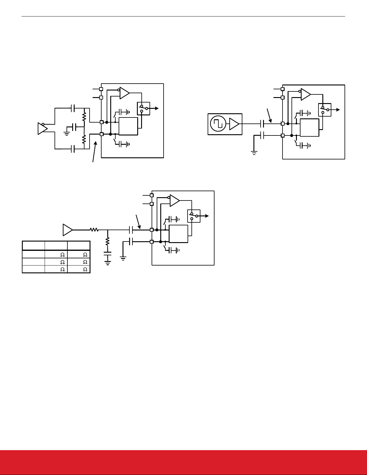
Si5386 Rev. E Reference Manual
XAXB External References
8. XAXB External References
8.1 Performance of External References
An external crystal oscillator (XO) is required to set the reference for the Si5386. Either a 54 MHz or 48.0231 MHz XO may be used as
the reference to the wireless jitter attenuator.
Differential Connection
0.1 uf
0.1 uf
0.1 uf
Note: 2.5 Vpp diff max
CMOS/XO Output
XO VDD R1 R2
3.3 V 523 442
2.5 V 475 649
1.8 V 158 866
X1
nc
X2
nc
50
XA
XB
50
Single-ended Connection
Note: 2. 0 Vpp_se max
R1
R2
0.1 uf
2xCL
2xCL
OSC
0.1 uf
0.1 uf
nc
nc
Si5386
X1
X2
XA
XB
2xCL
2xCL
OSC
XO with
Clipped Sine
Wave Output
Si5386
Single-ended XO Connection
X1
nc
X2
nc
Note: 2. 0 Vpp_se max
0.1 uf
XA
XB
0.1 uf
2xCL
OSC
2xCL
Si5386
Figure 8.1. XAXB External Reference Clock Connection Options
The Si5386 accepts a Clipped Sine wave, CMOS, or Differential reference clock on the XAXB interface. Most clipped sine wave and
CMOS XOs
have insufficient drive strength to drive a 50 Ω or 100 Ω load. For this reason, place the XO as close to the Si5386 as
possible to minimize PCB trace length. In addition, connect both the Si5386 and the XO directly to the same ground plane. The figure
above shows the recommended method of connecting a clipped sine wave XO to the Si5386. Because the Si5386 provides dc bias at
the XA and XB pins, the ~800 mV peak-peak swing can be input directly into XA after ac-coupling. Single-ended inputs must be connected to the XA pin with proper termination on the XB pin. Because the signal is single-ended in this case, the XB input is ac-coupled
to ground. The figure above also illustrates the recommended method of connecting a single-ended CMOS rail-to-rail output to the
XAXB inputs of the Si5386. The resistor network attenuates the swing to ensure that the maximum input voltage swing at the XA pin
remains below the datasheet specification. The signal is ac-coupled before connecting it to the Si5386 XA input with the XB input again
ac-grounded through a capacitor. For applications with loop bandwidth values less than 10 Hz that require low wander output clocks,
using an external TCXO as the XAXB reference source should be considered to avoid the wander of a crystal or regular XO.
silabs.com | Building a more connected world. Rev. 1.0 | 59
Page 60
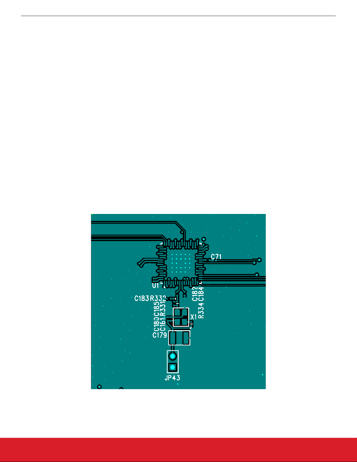
Si5386 Rev. E Reference Manual
XO and Device Circuit Layout Recommendations
9. XO and Device Circuit Layout Recommendations
The main layout issues that should be carefully considered for optimum phase noise include the following:
•
Number and size of the ground/thermal vias for the Epad (see 10.4 Grounding Vias)
• Output clock trace routing
• Input clock trace routing
• Control and Status signals to input or output clock trace coupling
Si5386A-E-EVB schematics, layouts, and component BOM files are available at: http://www.silabs.com/Si538x-4x-EVB.
9.1 Si5386 64-Pin QFN External XO Layout Recommendations
This section details the recommended guidelines for the layout of the 64-pin QFN Si5386 with external XO using the 8-layer Si5386A-EEB PCB. The following are the descriptions of each of the eight layers.
• Layer 1: device layer, with low speed CMOS control/status signals, ground flooded
• Layer 2: input clocks, ground flooded
• Layer 3: ground plane
• Layer 4: power distribution, ground flooded
• Layer 5: power routing layer
• Layer 6: ground input clocks, ground flooded
• Layer 7: output clocks layer
• Layer 8: ground layer
External XO: The figure below shows the top layer layout of the Si5386 device mounted on the PCB. The XO is outlined with the white
box around it. The top layer is flooded with ground. Both the XA and XB pins are capacitively coupled, with XB ac connected to XO
ground for single-ended output XO's. Notice the 5x5 array of thermal vias in the center of the device. See 10.4 Grounding Vias for more
information on thermal/ground via layout.
Figure 9.1. External XO: Si5386 Device and XO Layout Recommendations, Top Layer (Layer 1)
silabs.com | Building a more connected world. Rev. 1.0 | 60
Page 61

Si5386 Rev. E Reference Manual
XO and Device Circuit Layout Recommendations
External XO: The following figure shows the layer that implements the ground shield underneath the XO. This layer also has the clock
input pins.
ground shield above, below, and on the sides for maximum protection.
The clock input pins go to layer 2 using vias to avoid crosstalk. As soon as the clock inputs are on layer 2, they have a
Figure 9.2. External XO: Input Clocks and Ground Fill, Below the Top Layer (Layer 2)
silabs.com | Building a more connected world. Rev. 1.0 | 61
Page 62

Si5386 Rev. E Reference Manual
XO and Device Circuit Layout Recommendations
External XO: The figure below shows one of the ground planes. Figure 9.4
a power plane and shows the clock output power supply traces.
External XO: Internal Power Plane (Layer 4) on page 62 is
Figure 9.3. External XO: Internal Ground Plane (Layer 3)
Figure 9.4. External XO: Internal Power Plane (Layer 4)
silabs.com | Building a more connected world. Rev. 1.0 | 62
Page 63

Si5386 Rev. E Reference Manual
XO and Device Circuit Layout Recommendations
External XO: The figure below shows layer 5, which is the power plane routed to the clock output power pins.
Figure 9.5. External XO: Internal Power Plane (Layer 5)
External XO: The figure below shows layer 6, another ground plane similar to layer 3.
Figure 9.6. External XO: Internal Ground Plane (Layer 6)
silabs.com | Building a more connected world. Rev. 1.0 | 63
Page 64

Si5386 Rev. E Reference Manual
XO and Device Circuit Layout Recommendations
External XO: The figure below shows the output clocks. Similar to the input clocks, the output clocks have vias that immediately go to a
buried layer
pairs to reduce crosstalk. There should be a line of vias through the ground flood on either side of the output clocks to ensure that the
ground flood immediately next to the differential pairs has a low inductance path to the ground plane on layers 3 and 6.
with a ground plane above them and a ground flooded bottom layer. There is ground flooding between the clock output
Figure 9.7. External XO: Output Clocks (Layer 7)
silabs.com | Building a more connected world. Rev. 1.0 | 64
Page 65

Si5386 Rev. E Reference Manual
XO and Device Circuit Layout Recommendations
External XO: The bottom layer shown in the figure below displays the location of the decoupling capacitors close to the device.
Figure 9.8. External XO: Bottom Layer Ground Flooded (Layer 8)
silabs.com | Building a more connected world. Rev. 1.0 | 65
Page 66

Si5386 Rev. E Reference Manual
Power Management
10. Power Management
10.1 Power Management Features
A number of unused functions can be powered down to minimize power consumption. The registers listed in the table below are used
for powering down different features of the device.
Table 10.1. Powerdown Registers
Register Name Hex Address [Bit Field] Function
PDN 0x001E[0] Place the device into a low current Power-
down state. Note that the serial interface
and registers remain active in this state.
0: Normal Operation (default)
1: Powerdown Device
OUT0A_PDN
OUT0_PDN
OUT1_PDN
OUT2_PDN
OUT3_PDN
OUT4_PDN
OUT5_PDN
OUT6_PDN
OUT7_PDN
OUT8_PDN
OUT9_PDN
OUT9A_PDN
OUT_PDN_ALL 0x0145[0] Powers down all output drivers.
IN_EN 0x0949[3:0] Enable (or powerdown) the IN3 - IN0 input
0x0103[0]
0x0108[0]
0x010D[0]
0x0112[0]
0x0117[0]
0x011C[0]
0x0121[0]
0x0126[0]
0x012B[0]
0x0130[0]
0x0135[0]
0x013A[0]
Powers down unused output drivers.
0: Power-up output driver (default)
1: Powerdown output driver
When powered down, output pins will be
high impedance with a light pull down effect.
0: Normal Operation (default)
1: Powerdown All output drivers
buffers.
0: Powerdown input buffer
1: Enable and Power-up input buffer
10.2 Power Supply Recommendations
supply
Power
tion to minimize the impact of board level noise on clock jitter. Following conventional power supply filtering and layout techniques will
minimize signal degradation from power supply noise.
It is recommended to use a 0402-size 1 mF ceramic capacitor on each power supply pin for optimal performance. If the supply voltage
is extremely noisy, it might require a ferrite bead in series between the voltage supply voltage and the device power supply pin.
silabs.com | Building a more connected world. Rev. 1.0 | 66
filtering is generally important for optimal timing performance. The Si5386 devices have multiple stages of on-chip regula-
Page 67

10.3 Power Supply Sequencing
Si5386 Rev. E Reference Manual
Power Management
Four classes of supply voltages exist on the Si5386
:
1. VDD = 1.8 V (Core digital supply)
2. VDDA = 3.3 V (Analog supply)
3. VDDO = 1.8/2.5/3.3 V (Output Clock supplies)
There is no general requirement for power supply sequencing on this device unless the output clocks are required to be phase
aligned with each other. In this case, the VDDO of each clock which needs to be aligned must be powered up before VDD and
VDDA.
If output-to-output alignment is required for applications where it is not possible to properly sequence the power supplies, then the
output clocks can be aligned by asserting Hard Reset 0x001E[1] register bits or driving the RSTb pin. Note that using a Hard Reset
will reload the register with the contents of the NVM and any unsaved register changes will be lost.
When powering up the VDD = 1.8V rail first, it can be observed that the VDDA = 3.3 V rail will initially follow the 1.8 V rail. Likewise,
if the VDDA rail is powered down first then it will not drop far below VDD until VDD itself is powered down. This is due to the pad
I/O circuits, which have large MOSFET switches to select the local supply from either the VDD or VDDA rails. These devices are
relatively large and yield a parasitic diode between VDD and VDDA. Allow for both VDD and VDDA to power-up and power-down
before measuring their respective voltages.
10.4 Grounding Vias
The "Epad" on the bottom of the device functions as both the sole electrical ground and as the primary heat transfer path. Hence it is
important to minimize the inductance and maximize the heat transfer from this pad to the internal ground plane of the PCB. Use no
fewer than 25 vias from the center pad to a ground plane under the device. In general, more vias will perform better. Having the ground
plane near the top layer will also help to minimize the via inductance from the device to ground and maximize the heat transfer away
from the device.
silabs.com | Building a more connected world. Rev. 1.0 | 67
Page 68

Si5386 Rev. E Reference Manual
Base vs. Factory Preprogrammed Devices
11. Base vs. Factory Preprogrammed Devices
The Si5386 devices can be ordered as "base" or "factory-preprogrammed" (also known as "custom OPN") versions.
11.1 "Base" Devices (a.k.a. "Blank" Devices)
• Example "base" orderable part numbers (OPNs) are of the form "Si5386A-E-GM."
• Base devices are available for applications where volatile reads and writes are used to program and configure the device for a particular application.
• Base devices do not power up in a usable state (all output clocks are disabled).
•
Base devices are, however, configured by default to use a 1.8 V compatible I/O voltage setting for the host I2C/SPI and external 54
MHz XO as the reference clock by default.
• Additional programming of a base device is mandatory to achieve a usable configuration.
• See the on-line lookup utility at www.silabs.com/products/clocksoscillators/pages/clockbuilderlookup.aspx to access the default configuration plan and register settings for any base OPN.
11.2 "Factory Preprogrammed" (Custom OPN) Devices
• Factory preprogammed devices use a “custom OPN”, such as Si5386A-Exxxxx-GM, where “xxxxx” is a sequence of characters assigned by Silicon Labs for each customer-specific configuration. These characters are referred to as the “OPN ID”. Customers must
initiate custom OPN creation using the ClockBuilder Pro software.
• Many customers prefer to order devices which are factory preprogrammed for a particular application that includes specifying the
clock input frequencies, the clock output frequencies, as well as the other options, such as automatic clock selection, loop bandwidth, etc. The ClockBuilder software is required to select among all of these options and to produce a project file which Silicon Labs
uses to preprogram all devices with custom orderable part number (“custom OPN”).
• Custom OPN devices contain all of the initialization information in their non-volatile memory (NVM) so that it powers up fully configured and ready to go.
• Because preprogrammed device applications are inherently quite different from one another, the default power up values of the register settings can be determined using the custom OPN utility at: http://www.silabs.com/products/clocksoscillators/pages/clockbuil-
derlookup.aspx
• Custom OPN devices include a device top mark which includes the unique OPN ID. Refer to the device data sheet's Ordering Guide
and Top Mark sections for more details.
Both "base" and "factory preprogrammed" devices can have their operating configurations changed at any time using volatile reads and
writes to the registers. Both types of devices can also have their current register configuration written to the NVM by executing an NVM
bank burn sequence (see 2.1.2 NVM Programming).
11.3 Part Numbering Summary
Part numbers are of the form:
Si<Part Num Type><Grade>-<Device Revision><OPN ID>-<Temp Grade><Package ID>
For example:
• Si5386A-E12345-GM: Applies to a factory preprogrammed OPN (Ordering Part Number) device. These devices are programmed at
the factory with the frequency plan and all other operating characteristics defined by the user's ClockBuilder Pro project file.
• Si5386A-E-GM: Applies to a "base" device. Base devices are factory programmed to a specific base part type (e.g., Si5386) but
exclude any user-defined frequency plan or other operating characteristics which would be selected in ClockBuilder Pro.
silabs.com | Building a more connected world. Rev. 1.0 | 68
Page 69

Si5386 Rev. E Reference Manual
Register Map
12. Register Map
12.1 Page 0 Registers
Table 12.1. Register 0x0000 Die Rev
Reg Address Bit Field Type Name Default Description
0x0000 3:0 R DIE_REV 0 4-bit die revision number
Table 12.2. Register 0x0001 Page
Reg Address Bit Field Type Name Default Description
0x0001 7:0 R/W PAGE 0 Select one of 256 possible
pages.
This is the “Page Register” which is located at address 0x01 on every page. When read, it will indicate the current page. When written,
change the page to the value entered. There is a page register at address 0x0001, 0x0101, 0x0201, 0x0301, … etc. See "AN926:
it will
Reading and Writing Registers with SPI and I2C for Si534x/8x Devices" for more information on register paging.
Table 12.3. Register 0x0002-0x0003 Base Part Number
Reg Address Bit Field Type Name Default Description
0x0002 7:0 R PN_BASE 0x86 Four-digit ,"base" part num-
0x0003 15:8 R PN_BASE 0x53
See 11.3 Part Numbering Summary for more information on part numbers.
Table 12.4. Register 0x0004 Device Grade
Reg Address Bit Field Type Name Description
0x0004 7:0 R GRADE One ASCII character indicating the
See 11.3 Part Numbering Summary for more information on part numbers. Refer to the device data sheet Ordering Guide section for
more information about device grades.
ber, one nibble per digit. Example: Si5386A-E-GM. The
base part number is 5386,
which is stored in this register.
device speed grade. For example
Si5386A-E12345-GM would be 0,
grade A:
0 = A, 1 = B, 2 = C, 3 = D, 4 = E,
etc.
Table 12.5. Register 0x0005 Device Revision
Reg Address Bit Field Type Name Description
0x0005 7:0 R DEVICE_REV One ASCII character indicating the
device revision level.
0 = A; 1 = B; 2 = C, 3 = D, 4 = E,
etc.
For example: Si5386
GM, the device revision is E = 4.
silabs.com | Building a more connected world. Rev. 1.0 | 69
A-E12345-
Page 70

Si5386 Rev. E Reference Manual
Register Map
See 11.3 Part Numbering Summary for more information on part numbers. Refer to the device data sheet Ordering Guide section for
more information about device grades.
Table 12.6. Register 0x0009 Temperature Grade
Reg Address Bit Field Type Name Description
0x0009 7:0 R TEMP_GRADE Device temperature grade:
0: Industrial (-40 to 85 °C
See 11.3 Part Numbering Summary for more information on part numbers.
Table 12.7. Register 0x000A Package ID
Reg Address Bit Field Type Name Description
0x000A 7:0 R PKG_ID Package Identifier:
0: 64-pin 9x9 mm QFN
See 11.3 Part Numbering Summary for more information on part numbers.
Table 12.8. Register 0x000B I2C Address
Reg Address Bit Field Type Name Description
0x000B 6:0 R I2C_ADDR 7-bit I2C Address
Note that the two least significant bits, [1:0], are determined by the voltages on the A1 and A0 input pins, respectively. This setting is
not saved
as part of the usual NVM write procedure. To update this register in a non-volatile way, the "Si534x8x I2C Address Burn
Tool" allows updating this value one time. This utility is included in the ClockBuilder Pro installation and can be accessed under the
"Misc" folder in the installation directory.
Table 12.9. Register 0x000C Device Status
Reg Address Bit Field Type Name Description
0x000C 0 R SYSINCAL 1 if the device is currently calibrat-
ing.
0x000C 1 R LOSXAXB 1 if there is currently no signal from
the XAXB reference clock.
0x000C 2 R LOSREF 1 if there is currently no signal from
the XAXB reference clock.
0x000C 3 R XAXB_ERR 1 if there is currently a problem
locking to the XAXB reference
clock.
0x000C 5 R SMBUS_TIMEOUT 1 if there is currently an SMB Bus
Timeout error.
See 3.3 Fault Monitoring for more information.
Table 12.10. Register 0x000D Out-of-Frequency (OOF) and Loss-of Signal (LOS) Status
Reg Address Bit Field Type Name Description
0x000D 3:0 R LOS 1 if IN3 - IN0 is currently LOS
0x000D 7:4 R OOF 1 if IN3 - IN0 is currently OOF
silabs.com | Building a more connected world. Rev. 1.0 | 70
Page 71
Si5386 Rev. E Reference Manual
See 3.3 Fault Monitoring for more information.
• IN0: LOS 0x000D[0], OOF 0x000D[4]
IN1: LOS 0x000D[1], OOF 0x000D[5]
•
• IN2: LOS 0x000D[2], OOF 0x000D[6]
• IN3/FB_IN: LOS 0x000D[3], OOF 0x000D[7]
Table 12.11. Register 0x000E Holdover (HOLD) and Loss-of-Lock (LOL) Status
Reg Address Bit Field Type Name Description
0x000E 1 R LOL 1 if the DSPLL is currently out of
lock
0x000E 5 R HOLD 1 if the DSPLL is currently in Hold-
over or Freerun
See 3.3 Fault Monitoring for more information.
Table 12.12. Register 0x000F DSPLL Calibration Status
Reg Address Bit Field Type Name Description
Register Map
0x000F 5 R CAL 1 if the DSPLL internal calibration
is currently busy
See 3.3 Fault Monitoring for more information.
Table 12.13. Register 0x0011 Device Status Flags
Reg Address Bit Field Type Name Description
0x0011 0 R/W SYSINCAL_FLG Flag 1 if the device was in SYSINCAL
0x0011 1 R/W LOSXAXB_FLG Flag 1 if the XAXB reference clock showed LOS-
XAXB
0x0011 2 R/W LOSREF_FLG Flag 1 if the XAXB reference clock LOSREF
0x0011 3 R/W XAXB_ERR_FLG Flag 1 if the XAXB reference clock showed
XAXB_ERR
0x0011 5 R/W SMBUS_TIMEOUT_FLG Flag 1 if SMBUS_TMEOUT ws in error
These are sticky flag bits corresponding to the bits in register 0x000C. They are cleared by writing 0 to the bit that has been set. The
corresponding 0x000C register bit must be 0 to clear this sticky flag bit. See 3.3 Fault Monitoring for more information.
Table 12.14. Register 0x0012 OOF and LOS Status Flags
Reg Address Bit Field Type Name Description
0x0012 3:0 R/W LOS_FLG Flag 1 if IN3 - IN0 was or is LOS
0x0012 7:4 R/W OOF_FLG Flag 1 if IN3 - IN0 was or is OOF
These are sticky flag bits corresponding to the bits in register 0x000D. They are cleared by writing 0 to the bit that has been set. The
corresponding 0x000D register bit must be 0 to clear this sticky flag bit. See 3.3 Fault Monitoring for more information.
• IN0: LOS_FLG 0x0012[0], OOF_FLG 0x0012[4]
•
IN1: LOS_FLG 0x0012[1], OOF_FLG 0x0012[5]
• IN2: LOS_FLG 0x0012[2], OOF_FLG 0x0012[6]
• IN3/FB_IN: LOS_FLG 0x0012[3], OOF_FLG 0x0012[7]
silabs.com | Building a more connected world. Rev. 1.0 | 71
Page 72

Si5386 Rev. E Reference Manual
Register Map
Table 12.15. Register 0x0013 HOLD and LOL Status Flags
Reg Address Bit Field Type Name Description
0x0013 1 R/W LOL_FLG Flag 1 if the DSPLL was or is LOL
0x0013 5 R/W HOLD_FLG Flag 1 if the DSPLL was or is in
Holdover or Freerun
These are sticky flag bits corresponding to the bits in register 0x000E. They are cleared by writing 0 to the bit that has been set. The
corresponding 0x000E register bit must be 0 to clear this sticky flag bit. See 3.3 Fault Monitoring for more information.
Table 12.16. Register 0x0014 DSPLL Calibration Status Flag
Reg Address Bit Field Type Name Description
0x0014 5 R/W CAL_FLG Flag 1 if the internal calibration was
or is busy
These are sticky flag bits corresponding to the bits in register 0x000F. They are cleared by writing 0 to the bit that has been set. The
corresponding 0x000F register bit must be 0 to clear this sticky flag bit. See 3.3 Fault Monitoring for more information.
Table 12.17. Register 0x0017 Device Status Interrupt Masks
Reg Address Bit Field Type Name Description
0x0017 0 R/W SYSINCAL_INTR_MSK 1 to mask SYSINCAL_FLG from
causing an interrupt
0x0017 1 R/W LOSXAXB_FLG_MSK 1 to mask LOSXAXB_FLG from
causing an interrupt
0x0017 2 R/W LOSREF_INTR_MSK 1 to mask LOSREF_FLG from
causing an interrupt
0x0017 3 R/W XAXB_ERR_INTR_MSK 1 to mask LOL_FLG from causing
an interrupt
0x0017 5 R/W SMBUS_IMOUT_ FLG_MSK 1 to mask SMBUS_TMOUT_FLG
from causing an interrupt
These are interrupt mask bits corresponding to the bits in register 0x0011. See 3.3.6 INTRb
Interrupt Configuration for more informa-
tion.
Table 12.18. Register 0x0018 OOF and LOS Interrupt Masks
Reg Address Bit Field Type Name Description
0x0018 3:0 R/W LOS_INTR_MSK 1 to mask LOS_FLG from causing
an interrupt
0x0018 7:4 R/W OOF_INTR_MSK 1 to mask OOF_FLG from causing
an interrupt
These are interrupt mask bits corresponding to the bits in register 0x0012. See 3.3.6 INTRb
Interrupt Configuration for more informa-
tion.
• IN0: LOS_INTR_MSK 0x0018[0], OOF_INTR_MSK 0x0018[4]
• IN1: LOS_INTR_MSK 0x0018[1], OOF_INTR_MSK 0x0018[5]
• IN2: LOS_INTR_MSK 0x0018[2], OOF_INTR_MSK 0x0018[6]
• IN3/FB_IN: LOS_INTR_MSK 0x0018[3], OOF_INTR_MSK 0x0018[7]
silabs.com | Building a more connected world. Rev. 1.0 | 72
Page 73

Si5386 Rev. E Reference Manual
Register Map
Table 12.19. Register 0x0019 HOLD and LOL Interrupt Masks
Reg Address Bit Field Type Name Description
0x0019 1 R/W LOL_INTR_MSK 1 to mask LOL_FLG from causing
an interrupt
0x0019 5 R/W HOLD_INTR_MSK 1 to mask HOLD_FLG from caus-
ing an interrupt
These are interrupt mask bits corresponding to the bits in register 0x0013. See 3.3.6 INTRb
Interrupt Configuration for more informa-
tion.
Table 12.20. Register 0x001A PLL In Calibration Interrupt Mask
Reg Address Bit Field Type Name Description
0x001A 5 R/W CAL_INTR_MSK 1 to mask CAL_FLG from causing
an interrupt
These are interrupt mask bits corresponding to the bits in register 0x0014. See 3.3.6 INTRb
Interrupt Configuration for more informa-
tion.
Table 12.21. Register 0x001C Soft Reset and Calibration
Reg Address Bit Field Type Name Description
0x001C 0 S SOFT_RST 1 Initialize and calibrate the device
0 No effect
Soft Reset restarts the device using the existing register values without loading from NVM. Soft Reset also updates registers requiring a
separate update strobe, including the DSPLL bandwidth registers as well as the P, M, N, and R dividers.
Table 12.22. Register 0x001E Sync, Power Down and Hard Reset
Reg Address Bit Field Type Name Description
0x001E 0 R/W PDN Place the device into a low current
Powerdown state. Note that the serial interface and registers remain
active in this state.
0: Normal Operation (default)
1: Powerdown Device
0x001E 1 S HARD_RST Perform Hard Reset with NVM
read.
0: Normal Operation
1: Hard Reset the device
0x001E 2 S SYNC Resets all R dividers. Logically
equivalent to asserting the SYNCb
pin.
0: Normal Operation
1: Reset R Dividers
silabs.com | Building a more connected world. Rev. 1.0 | 73
Page 74

Si5386 Rev. E Reference Manual
Register Map
Table 12.23. Register 0x0022 Output Enable Group Controls
Reg Address Bit Field Type Name Description
0x0022 0 R/W OE_REG_SEL Selects between Pin and Register
control for output disable.
0: OEb Pin disable (default)
1: OE Register disable
0x0022 1 R/W OE_REG_DIS When OE_REG_SEL = 1:
0: Disable selected outputs
1: Enable selected outputs
By default ClockBuilder Pro sets the OEb pin controlling all outputs. OUTALL_DISABLE_LOW (0x0102[0]) must be high (enabled) to
allow the
low). See 4.7.5 Output Driver Disable Source Summary for more information.
OEb pin to enable outputs. Note that the OE_REG_DIS bit (active high) has inverted logic sense from the OEb pin (active
Table 12.24. Register 0x002B SPI 3 vs 4 Wire
Reg Address Bit Field Type Name Description
0x002B 3 R/W SPI_3WIRE Selects operating mode for SPI in-
terface:
0: 4-wire SPI
1: 3-wire SPI
This bit is ignored for I2C bus operation, when I2C_SEL is high.
Table 12.25. Register 0x002C LOS Enables
Reg Address Bit Field Type Name Description
0x002C 3:0 R/W LOS_EN Enable LOS detection on IN3 - IN0.
0: Disable LOS Detection.
1: Enable LOS Detection.
0x002C 4 R/W LOSXAXB_DIS Enable LOS detection on the
XAXB reference clock.
0: Enable LOS Detection (default).
1: Disable LOS Detection.
• IN0: LOS_EN[0]
• IN1: LOS_EN[1]
IN2: LOS_EN[2]
•
• IN3/FB_IN: LOS_EN[3]
silabs.com | Building a more connected world. Rev. 1.0 | 74
Page 75

Si5386 Rev. E Reference Manual
Register Map
Table 12.26. Register 0x002D LOS Clear Delays
Reg Address Bit Field Type Name Description
0x002D 1:0 R/W LOS0_VAL_TIME IN0 LOS Clear delay.
0: 2 ms
1: 100 ms
2: 200 ms
3: 1000 ms
0x002D 3:2 R/W LOS1_VAL_TIME IN1, same as above
0x002D 5:4 R/W LOS2_VAL_TIME IN2, same as above
0x002D 7:6 R/W LOS3_VAL_TIME IN3/FB_IN, same as above
When a valid input clock is not present on the input, LOS will be asserted. When the clock returns, it must remain valid for this period of
time before that clock is considered to be qualified again.
Table 12.27. Register 0x002E-0x002F IN0 LOS Trigger Threshold
Reg Address Bit Field Type Name Description
0x002E 7:0 R/W LOS0_TRG_THR 16-bit LOS Trigger Threshold value
0x002F 15:8 R/W LOS0_TRG_THR
ClockBuilder Pro calculates the correct LOS register threshold trigger value for IN0, given a particular frequency plan.
Table 12.28. Register 0x0036-0x0037 LOS0 Clear Threshold
Reg Address Bit Field Type Name Description
0x0036 7:0 R/W LOS0_CLR_THR 16-bit LOS Clear Threshold value
0x0037 15:8 R/W LOS0_CLR_THR
ClockBuilder Pro calculates the correct LOS register clear threshold value for IN0, given a particular frequency plan.
All 4 input buffers are identical in terms of control. The single set of descriptions for IN0 above also apply to IN1-IN3.
Table 12.29. Output Registers Following the Same Definitions as IN0
Register Addresses Description (Same as) Addresses
0x0030 - 0x0031 IN1 LOS Trigger Threshold 0x002E - 0x002F
0x0038 - 0x0039 IN1 LOS Clear Threshold 0x0036 - 0x0037
0x0032 - 0x0033 IN2 LOS Trigger Threshold 0x002E - 0x002F
0x003A - 0x003B IN2 LOS Clear Threshold 0x0036 - 0x0037
0x0034 - 0x0035 IN3/FB_IN LOS Trigger Threshold 0x002E - 0x002F
0x003C - 0x003D IN3/FB_IN LOS Clear Threshold 0x0036 - 0x0037
silabs.com | Building a more connected world. Rev. 1.0 | 75
Page 76

Si5386 Rev. E Reference Manual
Register Map
Table 12.30. Register 0x003E LOS Min Period Enable
Reg Address Bit Field Type Name Description
0x003E 7:4 R/W LOS_MIN_PERI-
Values set by CBPro.
OD_EN
Table 12.31. Register 0x003F OOF Enable
Reg Address Bit Field Type Name Description
0x003F 3:0 R/W OOF_EN Enable Precision OOF for IN3 - IN0
0: Disable Precision OOF
1: Enable Precision OOF
0x003F 7:4 R/W FAST_OOF_EN Enable Fast OOF for IN3 - IN0
0: Disable Fast OOF
1: Enable Fast OOF
• IN0: OOF_EN[0], FAST_OOF_EN[4]
•
IN1: OOF_EN[1], FAST_OOF_EN[5]
IN2: OOF_EN[2], FAST_OOF_EN[6]
•
• IN3/FB_IN: OOF_EN[3], FAST_OOF_EN[7]
Table 12.32. Register 0x0040 OOF Reference Select
Reg Address Bit Field Type Name Description
0x0040 2:0 R/W OOF_REF_SEL Select reference 0 ppm
0: IN0
1: IN1
2: IN2
3: IN3
4: XAXB reference clock (default)
5-7: Reserved
Table 12.33. Register 0x0041 OOF0 Divider Select
Reg Address Bit Field Type Name Description
0x0041 4:0 R/W OOF0_DIV_SEL Values calculated by CBPro.
Table 12.34. Register 0x0042 OOF1 Divider Select
Reg Address Bit Field Type Name Description
0x0042 4:0 R/W OOF1_DIV_SEL Values calculated by CBPro.
silabs.com | Building a more connected world. Rev. 1.0 | 76
Page 77

Si5386 Rev. E Reference Manual
Register Map
Table 12.35. Register 0x0043 OOF2 Divider Select
Reg Address Bit Field Type Name Description
0x0043 4:0 R/W OOF2_DIV_SEL Values calculated by CBPro.
Table 12.36. Register 0x0044 OOF3 Divider Select
Reg Address Bit Field Type Name Description
0x0044 4:0 R/W OOF3_DIV_SEL Values calculated by CBPro.
Table 12.37. Register 0x0045 OOFXO Divider Select
Reg Address Bit Field Type Name Description
0x0045 4:0 R/W OOFXO_DIV_SEL Values calculated by CBPro.
Table 12.38. Register 0x0046-0x0049 Precision OOF Set Thresholds
Reg Address Bit Field Type Name Description
0x0046 7:0 R/W OOF0_SET_THR Precision OOF Set Threshold. The
0x0047 7:0 R/W OOF1_SET_THR
0x0048 7:0 R/W OOF2_SET_THR
0x0049 7:0 R/W OOF3_SET_THR
range is up to ±500 ppm in 1/16
ppm steps.
Set Threshold (ppm) =
OOFx_SET_THR x 1/16 ppm
OOF will be indicated if this is set
to 0.
Table 12.39. Register 0x004A-0x004D Precision OOF Clear Thresholds
Reg Address Bit Field Type Name Description
0x004A 7:0 R/W OOF0_CLR_THR Precision OOF Clear Threshold.
0x004B 7:0 R/W OOF1_CLR_THR
0x004C 7:0 R/W OOF2_CLR_THR
0x004D 7:0 R/W OOF3_CLR_THR
The range is up to ±500 ppm in
1/16 ppm steps.
Clear Threshold (ppm) =
OOFx_CLR_THR x ±1/16 ppm
Note that OOF will be indicated if
this is set to 0.
Table 12.40. Register 0x004E–0x04F OOF Detection Windows
Reg Address Bit Field Type Name Description
0x004E 2:0 R/W FAST_OOF0_DETWIN_SEL
0x004E 6:4 R/W FAST_OOF1_DETWIN_SEL
Values calculated by CBPro
0x004F 2:0 R/W FAST_OOF2_DETWIN_SEL
0x004F 6:4 R/W FAST_OOF3_DETWIN_SEL
silabs.com | Building a more connected world. Rev. 1.0 | 77
Page 78

Si5386 Rev. E Reference Manual
Register Map
Table 12.41. Register 0x0050 OOF on LOS Controls
Reg Address Bit Field Type Name Description
0x0050 3:0 R/W OOF_ON_LOS Values set by CBPro.
Table 12.42. Register 0x0051-0x0054 Fast OOF Set Thresholds
Reg Address Bit Field Type Name Description
0x0051 3:0 R/W FAST_OOF0_SET_THR Fast OOF Set Threshold. The range
0x0052 3:0 R/W FAST_OOF1_SET_THR
0x0053 3:0 R/W FAST_OOF2_SET_THR
0x0054 3:0 R/W FAST_OOF3_SET_THR
is from ±1,000 ppm to ±16,000 ppm
in 1000 ppm steps.
Fast Set Threshold (ppm) =
(FAST_OOFx_SET_THR + 1) x
±1000 ppm
Note that OOF will be indicated if
this is set to 0.
Table 12.43. Register 0x0055-0x0058 Fast OOF Clear Thresholds
Reg Address Bit Field Type Name Description
0x0055 3:0 R/W FAST_OOF0_CLR_THR Fast OOF Clear Threshold. The
0x0056 3:0 R/W FAST_OOF1_CLR_THR
0x0057 3:0 R/W FAST_OOF2_CLR_THR
0x0058 3:0 R/W FAST_OOF3_CLR_THR
range is from ±1,000 ppm to
±16,000 ppm in 1000 ppm steps.
Fast Clear Threshold (ppm) =
(FAST_OOFx_CLR_THR + 1) *
±1000ppm
Note that OOF will be indicated if
this is set to 0.
Table 12.44. Register 0x0059 Fast OOF Detection Window
Reg Address Bit Field Type Name Description
0x0059 1:0 R/W FAST_OOF0_DETWIN_SEL
0x0059 3:2 R/W FAST_OOF1_DETWIN_SEL
Values calculated by CBPro
0x0059 5:4 R/W FAST_OOF2_DETWIN_SEL
0x0059 7:6 R/W FAST_OOF3_DETWIN_SEL
Table 12.45. Register 0x005A–0x05D OOF0 Ratio for Reference
Reg Address Bit Field Type Name Description
0x005A 7:0 R/W OOF0_RATIO_REF
0x005B 15:8 R/W OOF0_RATIO_REF
Values calculated by CBPro
0x005C 23:16 R/W OOF0_RATIO_REF
0x005D 25:24 R/W OOF0_RATIO_REF
silabs.com | Building a more connected world. Rev. 1.0 | 78
Page 79

Si5386 Rev. E Reference Manual
Register Map
Table 12.46. Register 0x005E–0x061 OOF1 Ratio for Reference
Reg Address Bit Field Type Name Description
0x005E 7:0 R/W OOF1_RATIO_REF
0x005F 15:8 R/W OOF1_RATIO_REF
Values calculated by CBPro
0x0060 23:16 R/W OOF1_RATIO_REF
0x0061 25:24 R/W OOF1_RATIO_REF
Table 12.47. Register 0x0062–0x065 OOF2 Ratio for Reference
Reg Address Bit Field Type Name Description
0x0062 7:0 R/W OOF2_RATIO_REF
0x0063 15:8 R/W OOF2_RATIO_REF
Values calculated by CBPro
0x0064 23:16 R/W OOF2_RATIO_REF
0x0065 25:24 R/W OOF2_RATIO_REF
Table 12.48. Register 0x0066–0x069 OOF3 Ratio for Reference
Reg Address Bit Field Type Name Description
0x0066 7:0 R/W OOF3_RATIO_REF
0x0067 15:8 R/W OOF3_RATIO_REF
Values calculated by CBPro
0x0068 23:16 R/W OOF3_RATIO_REF
0x0069 25:24 R/W OOF3_RATIO_REF
Table 12.49. Register 0x0092 Fast LOL Enable
Reg Address Bit Field Type Name Description
Fast LOL Enable. Large input frequency errors will quickly assert
LOL when enabled.
0x0092 1 R/W LOL_FST_EN
0: Disable Fast LOL
1: Enable Fast LOL (default)
Table 12.50. Register 0x0093 Fast LOL Detection Window
Reg Address Bit Field Type Name Description
0x0093 7:4 R/W LOL_FST_DETWIN_SEL Values calculated by CBPro
Table 12.51. Register 0x0095 Fast LOL Detection Value
Reg Address Bit Field Type Name Description
0x0095 3:2 R/W LOL_FST_VALWIN_SEL Values calculated by CBPro
silabs.com | Building a more connected world. Rev. 1.0 | 79
Page 80

Si5386 Rev. E Reference Manual
Register Map
Table 12.52. Register 0x0096 Fast LOL Set Threshold
Reg Address Bit Field Type Name Description
0x0096 7:4 R/W LOL_FST_SET_THR_SEL Values calculated by CBPro
Table 12.53. Register 0x0098 Fast LOL Clear Threshold
Reg Address Bit Field Type Name Description
0x0098 7:4 R/W LOL_FST_CLR_THR_SEL Values calculated by CBPro
Table 12.54. Register 0x009A LOL Enable
Reg Address Bit Field Type Name Description
0x009A 1 R/W LOL_SLOW_EN_PLL Enable LOL detection.
0: LOL Disabled
1: LOL Enabled
Table 12.55. Register 0x009B LOL Detection Window
Reg Address Bit Field Type Name Description
0x009B 7:4 R/W LOL_SLW_DETWIN_SEL Values calculated by CBPro
Table 12.56. Register 0x009D LOL Detection Window
Reg Address Bit Field Type Name Description
0x009D 3:2 R/W LOL_SLW_VALWIN_SEL Values calculated by CBPro
Table 12.57. Register 0x009E LOL Set Threshold
Reg Address Bit Field Type Name Description
0x009E 7:4 R/W LOL_SLW_SET_THR LOL Set Threshold.
See the list below for settings.
Table 12.58. Register 0x00A0 LOL Clear Threshold
Reg Address Bit Field Type Name Description
0x00A0 7:4 R/W LOL_SLW_CLR_THR LOL Clear Threshold.
See the list below for settings.
LOL_SET_THR and LOL_CLR_THR Threshold settings:
•
0 = ±0.1 ppm
1 = ±0.3 ppm
•
• 2 = ±1 ppm
• 3 = ±3 ppm
• 4 = ±10 ppm
• 5 = ±30 ppm
silabs.com | Building a more connected world. Rev. 1.0 | 80
Page 81

Si5386 Rev. E Reference Manual
• 6 = ±100 ppm
• 7 = ±300 ppm
8 = ±1000 ppm
•
• 9 = ±3000 ppm
• 10 = ±10000 ppm
• 11–15: Reserved
Table 12.59. Register 0x00A2 LOL Timer Enable
Reg Address Bit Field Type Name Description
0x00A2 1 R/W LOL_TIMER_EN Enable Delay for LOL Clear.
0: Disable Delay for LOL Clear
1: Enable Delay for LOL Clear
Extends the time after a clock returns or stabilizes before LOL de-asserts.
Table 12.60. Register 0x00A8-0x00AC LOL Clear Delay
Reg Address Bit Field Type Name Description
Register Map
0x00A9 7:0 R/W LOL_CLR_DELAY_DIV256 29-bit value
0x00AA 15:8
0x00AB 23:16
0x00AC 28:24
The LOL Clear Delay value is set by ClockBuilder Pro based on each frequency plan.
Table 12.61. Register 0x00E2 NVM Active Bank
Reg Address Bit Field Type Name Description
0x00E2 7:0 R ACTIVE_NVM_BANK 0x03 when no NVM has been
burned
0x0F when 1 NVM bank has been
burned
0x3F when 2 NVM banks have
been burned
hen ACTIVE_NVM_BANK = 0x3F,
the last bank has already been
burned. See 2.1.2 NVM Program-
ming for a detailed description of
how to program the NVM.
Table 12.62. Register 0x00E3 NVM Write Control
Reg Address Bit Field Type Name Description
0x00E3 7:0 R/W NVM_WRITE Write 0xC7 to initiate an NVM bank
burn.
See 2.1.2 NVM Programming for more information.
silabs.com | Building a more connected world. Rev. 1.0 | 81
Page 82

Si5386 Rev. E Reference Manual
Register Map
Table 12.63. Register 0x00E4 Read Active NVM Bank
Reg Address Bit Field Type Name Description
0x00E4 0 S NVM_READ_BANK Set to 1 to initiate NVM copy to
registers.
Table 12.64. Register 0x00E5 Fastlock Extend Enable
Reg Address Bit Field Type Name Description
0x00E5 5 R/W FASTLOCK_EXTEND_EN Extend Fastlock bandwidth period
past LOL Clear
0: Do not extend Fastlock period
1: Extend Fastlock period (default)
Table 12.65. Register 0x00EA-0x00ED Fastlock Extend Length
Reg Address Bit Field Type Name Description
0x00EA 7:0 R/W FASTLOCK_EXTEND Values calculated by CBPro to mini-
0x00EB 15:8 R/W FASTLOCK_EXTEND
0x00EC 23:16 R/W FASTLOCK_EXTEND
mize transients when switching to
or from the Fastlock bandwidth.. 29-
bit value.
0x00ED 28:24 R/W FASTLOCK_EXTEND
Table 12.66. Register 0x00FE Device Ready
Reg Address Bit Field Type Name Description
0x00FE 7:0 R DEVICE_READY Device Ready indicator.
0x0F: Device is Ready
0xF3: Device is Not ready
Read-only byte to indicate when the device is ready to accept serial bus writes. The user can poll this byte starting at power-up. When
reads from DEVICE_READY return 0x0F the user can safely read or write to all registers. This is generally only needed after POR, after
a Hard
Reset by pin or register, or after initiating and NVM write. The “Device Ready” register is available on every page in the device
at the second to the last serial address, 0xFE. There is a device ready register at 0x00FE, 0x01FE, 0x02FE, … etc. Since this is on
every page, you should not write the page register when reading DEVICE_READY.
silabs.com | Building a more connected world. Rev. 1.0 | 82
Page 83

Si5386 Rev. E Reference Manual
12.2 Page 1 Registers
Table 12.67. Register 0x0102 Global Output Gating for all Clock Outputs
Reg Address Bit Field Type Name Description
0x0102 0 R/W OUTALL_DISABLE_LOW Enable/Disable All output drivers. If
the OEb pin is held high, then all
outputs will be disabled regardless
of this setting.
0: Disable All outputs (default)
1: Enable All outputs
Table 12.68. Register 0x0103 OUT0A Output Enable and R0A Divider Configuration
Reg Address Bit Field Type Name Description
0x0103 0 R/W OUT0A_PDN Powerdown output driver.
0: Normal Operation (default)
Register Map
1: Powerdown output driver
When powered down, outputs pins
will be high impedance with a light
pull down effect.
0x0103 1 R/W OUT0A_OE Enable/Disable individual output.
0: Disable output (default)
1: Enable output
0x0103 2 R/W OUT0A_RDIV_FORCE Force R0A output divider divide-
by-2.
0: R0A_REG sets divide value (default)
1: Divide value forced to divide-by-2
0x0103 3 R/W OUT0A_DIV2_BYP Output divide-by-2 bypass
0: Use output divide-by-2 (default)
1: Disable output divide-by-2
Setting R0A_REG = 0 will not set the divide value to divide-by-2 automatically. OUT0A_RDIV_FORCE must be set to a value of 1 to
force R0A
to divide-by-2. Note that the R0A_REG value will be ignored while OUT0A_RDIV_FORCE = 1. See R0A_REG registers,
0x0247-0x0249, for more information. Setting OUTx_DIV2_BYP = 1, the output clock duty cycle will be set by the N output divider value.
silabs.com | Building a more connected world. Rev. 1.0 | 83
Page 84

Si5386 Rev. E Reference Manual
Register Map
Table 12.69. Register 0x0104 OUT0A Output Format and Configuration
Reg Address Bit Field Type Name Description
0x0104 2:0 R/W OUT0A_FORMAT Select output format.
0: Reserved
1: Differential Normal
mode
2: Differential Low-Power
mode
3: Reserved
4: LVCMOS single ended
5: LVCMOS (OUTx pin
only)
6: LVCMOS (OUTxb pin
only)
7: Reserved
0x0104 3 R/W OUT0A_SYNC_EN Synchronous Enable/
Disable selection.
0: Asynchronous Enable/
Disable (default)
1: Synchronous Enable/
Disable (Glitchless)
0x0104 5:4 R/W OUT0A_DIS_STATE Determines the logic
state of the output driver
when disabled:
0: Disable logic Low
1: Disable logic High
2-3: Reserved
0x0104 7:6 R/W OUT0A_CMOS_DRV LVCMOS output impe-
dance selection. See Ta-
ble 4.8 LVCMOS Output
Impedance and Drive
Strength Selections
on
page 40for valid selec-
tions.
Table 12.70. Register 0x0105 Output OUT0A Differential Amplitude and Common Mode
Reg Address Bit Field Type Name Description
0x0105 3:0 R/W OUT0A_CM OUT0A Common Mode
Voltage selection. Only
applies when
OUT0A_FORMAT=1 or
2.
0x0105 6:4 R/W OUT0A_AMPL OUT0A Differential Am-
plitude setting. Only applies when OUT0A_FORMAT=1 or 2.
silabs.com | Building a more connected world. Rev. 1.0 | 84
Page 85

Si5386 Rev. E Reference Manual
Register Map
ClockBuilder Pro is used to select the correct settings for this register. See Table 4.7
Recommended Settings for Differential LVPECL,
LVDS, HCSL, and CML on page 38 and 13. Appendix—Custom Differential Amplitude Controls for details of the settings.
Table 12.71. Register 0x0106 Output OUT0A Source, VDD Select, and LVCMOS Inversion
Reg Address Bit Field Type Name Description
0x0106 2:0 R/W OUT0A_MUX_SEL OUT0A output source divider select.
0: N0 is the source for OUT0A
1: N1 is the source for OUT0A
2: N2 is the source for OUT0A
3: N3 is the source for OUT0A
4: N4 is the source for OUT0A
5-7: Reserved
0x0106 3 R/W OUT0A_VDD_SEL_EN Output Driver VDD Select Enable. Set to 1
for normal operation.
0x0106 5:4 R/W OUT0A_VDD_SEL Output Driver VDD Select
0: 3.3V
1: 1.8V
2: 2.5V
3: Reserved
0x0106 7:6 R/W OUT0A_INV OUT0A output LVCMOS inversion. Only
applies when OUT0A_FORMAT= 4. See
Table 4.10 LVCMOS Output Polarity Registers on page
for more information.
41
Each output can be independently configured to use one of the N0-N4 divider outputs as its source. Nx_NUM and Nx_DEN for each Ndivider are
set in registers 0x0302-0x0337 for N0 to N4. Five different frequencies can be set in the N-dividers (N0-N4) and each of the
12 outputs can be configured to use any of the five different frequencies.
All 12 output drivers are identical in terms of control. The single set of descriptions above for OUT0A also applies to OUT0-OUT9A:
Table 12.72. Register 0x0107 Output Disable Source DSPLL
Register Address Bit Field Type Setting Name Description
0x0107 2:0 R/W OUT0A_DIS_SRC Output clock Squelched (temporary disa-
ble) on DSPLL Soft Reset:
0-1: Reserved
2: DSPLL squelches output
3-7: Reserved
Note:
1. The CLKx_DIS_SRC settings should match the corresponding OUTx_MUX_SEL selections. The setting codes for
OUTx_DIS_SRC and OUTx_MUX_SEL are different when selecting the same DSPLL.
silabs.com | Building a more connected world. Rev. 1.0 | 85
Page 86

Si5386 Rev. E Reference Manual
Table 12.73. Output Registers Following the Same Definitions as OUT0A
Register Address Description (Same as) Address
Register Map
0x0108 OUT0 Powerdown, Output Enable,
0x0103
and R0 Divide-by-2
0x0109 OUT0 Signal Format and Configura-
0x0104
tion
0x010A OUT0 Differential Amplitude and
0x0105
Common Mode
0x010B OUT0 Source Selection and
0x0106
LVCMOS Inversion
0x010C OUT0 Disable Source 0x0107
0x010D OUT1 Powerdown, Output Enable,
0x0103
and R1 Divide-by-2
0x010E OUT1 Signal Format and Configura-
0x0104
tion
0x010F OUT1 Differential Amplitude and
0x0105
Common Mode
0x0110 OUT1 Source Selection and
0x0106
LVCMOS Inversion
0x0111 OUT1 Disable Source 0x0107
0x0112 OUT2 Powerdown, Output Enable,
0x0103
and R2 Divide-by-2
0x0113 OUT2 Signal Format and Configura-
0x0104
tion
0x0114 OUT2 Differential Amplitude and
0x0105
Common Mode
0x0115 OUT2 Source Selection and
0x0106
LVCMOS Inversion
0x0116 OUT2 Disable Source 0x0107
0x0117 OUT3 Powerdown, Output Enable,
0x0103
and R3 Divide-by-2
0x0118 OUT3 Signal Format and Configura-
0x0104
tion
0x0119 OUT3 Differential Amplitude and
0x0105
Common Mode
0x011A OUT3 Source Selection and
0x0106
LVCMOS Inversion
0x011B OUT3 Disable Source 0x0107
0x011C OUT4 Powerdown, Output Enable,
0x0103
and R4 Divide-by-2
0x011D OUT4 Signal Format and Configura-
0x0104
tion
0x011E OUT4 Differential Amplitude and
0x0105
Common Mode
silabs.com | Building a more connected world. Rev. 1.0 | 86
Page 87

Si5386 Rev. E Reference Manual
Register Address Description (Same as) Address
Register Map
0x011F OUT4 Source Selection and
0x0106
LVCMOS Inversion
0x0120 OUT4 Disable Source 0x0107
0x0121 OUT5 Powerdown, Output Enable,
0x0103
and R5 Divide-by-2
0x0122 OUT5 Signal Format and Configura-
0x0104
tion
0x0123 OUT5 Differential Amplitude and
0x0105
Common Mode
0x0124 OUT5 Source Selection and
0x0106
LVCMOS Inversion
0x0125 OUT5 Disable Source 0x0107
0x0126 OUT6 Powerdown, Output Enable,
0x0103
and R6 Divide-by-2
0x0127 OUT6 Signal Format and Configura-
0x0104
tion
0x0128 OUT6 Differential Amplitude and
0x0105
Common Mode
0x0129 OUT6 Source Selection and
0x0106
LVCMOS Inversion
0x012A OUT6 Disable Source 0x0107
0x012B OUT7 Powerdown, Output Enable,
0x0103
and R7 Divide-by-2
0x012C OUT7 Signal Format and Configura-
0x0104
tion
0x012D OUT7 Differential Amplitude and
0x0105
Common Mode
0x012E OUT7 Source Selection and
0x0106
LVCMOS Inversion
0x012F OUT7 Disable Source 0x0107
0x0130 OUT8 Powerdown, Output Enable,
0x0103
and R8 Divide-by-2
0x0131 OUT8 Signal Format and Configura-
0x0104
tion
0x0132 OUT8 Differential Amplitude and
0x0105
Common Mode
0x0133 OUT8 Source Selection and
0x0106
LVCMOS Inversion
0x0134 OUT8 Disable Source 0x0107
0x0135 OUT9 Powerdown, Output Enable,
0x0103
and R9 Divide-by-2
0x0136 OUT9 Signal Format and Configura-
0x0104
tion
0x0137 OUT9 Differential Amplitude and
0x0105
Common Mode
silabs.com | Building a more connected world. Rev. 1.0 | 87
Page 88

Si5386 Rev. E Reference Manual
Register Address Description (Same as) Address
Register Map
0x0138 OUT9 Source Selection and
0x0106
LVCMOS Inversion
0x0139 OUT9 Disable Source 0x0107
0x013A OUT9A Powerdown, Output Enable,
0x0103
and R9A Divide-by-2
0x013B OUT9A Signal Format and Configu-
0x0104
ration
0x013C OUT9A Differential Amplitude and
0x0105
Common Mode
0x013D OUT9A Source Selection and
0x0106
LVCMOS Inversion
0x013E OUT9A Disable Source 0x0107
Table 12.74. Register 0x013F-0x0140 Output Disable Mask for ZDM
Reg Address Bit Field Type Name Description
0x013F 7:0 R/W OUTX_ALWAYS_ON Force output driver to remain active, even
when fault conditions are present. Used
primarily for ZDM.
0: Normal output driver enable/disable
(default)
1: Force driver always active (ZDM)
[OUT6, OUT5, ..., OUT0, OUT0A]
0x0140 3:0 R/W OUTX_ALWAYS_ON [OUT9A, OUT9, OUT8, OUT7]
Table 12.75. Register 0x0141 Output Disable Mask for LOSXAXB
Reg Address Bit Field Type Name Description
0x0141 1 R/W OUT_DIS_MSK Mask alarms from disabling all out-
put drivers.
0: Disable All output drivers on
alarm (default)
1: Ignore alarms for output driver
disable
0x0141 6 R/W OUT_DIS_LOSXAXB_MSK Mask LOSXAXB from disabling all
output drivers.
0: Disable All output drivers on
LOSXAXB (default)
1: Ignore LOSXAXB for output driver disable
See 4.7.5 Output Driver Disable Source Summaryfor more information.
silabs.com | Building a more connected world. Rev. 1.0 | 88
Page 89

Si5386 Rev. E Reference Manual
Table 12.76. Register 0x0142 Output Disable Mask for LOL
Reg Address Bit Field Type Name Description
0x0142 1 R/W OUT_DIS_MASK_LOL Mask LOL from disabling all output
drivers.
0: Disable All output drivers on
LOL (default)
1: Ignore LOL for output driver disable
See 4.7.5 Output Driver Disable Source Summaryfor more information.
Table 12.77. Register 0x0145 Output Power Down All
Reg Address Bit Field Type Name Description
0x0145 0 R/W OUT_PDN_ALL Powerdown all output drivers.
0: Normal Operation (default)
Register Map
1: Powerdown all output drivers
silabs.com | Building a more connected world. Rev. 1.0 | 89
Page 90

Si5386 Rev. E Reference Manual
12.3 Page 2 Registers
Table 12.78. Register 0x0208-0x020D P0 Divider Numerator
Reg Address Bit Field Type Name Description
0x0208 7:0 R/W P0_NUM 48-bit Integer Number
0x0209 15:8
0x020A 23:16
0x020B 31:24
0x020C 39:32
0x020D 47:40
Table 12.79. Register 0x020E-0x0211 P0 Divider Denominator
Reg Address Bit Field Type Name Description
0x020E 7:0 R/W P0_DEN 32-bit Integer Number
Register Map
0x020F 15:8
0x0210 23:16
0x0211 31:24
The P input divider values are calculated by ClockBuilder Pro for a particular frequency plan and are written into these registers. The
new register values for the P divider will not take effect until the appropriate Px_UPDATE strobe is set as described below.
Table 12.80. Registers that Follow the P0_NUM and P0_DEN Above
Register Address Description Size Same as Address
0x0212-0x0217 P1 Divider Numerator 48-bit Integer Number 0x0208-0x020D
0x0218-0x021B P1 Divider Denominator 32-bit Integer Number 0x020E-0x0211
0x021C-0x0221 P2 Divider Numerator 48-bit Integer Number 0x0208-0x020D
0x0222-0x0225 P2 Divider Denominator 32-bit Integer Number 0x020E-0x0211
0x0226-0x022B P3 Divider Numerator 48-bit Integer Number 0x0208-0x020D
0x022C-0x022F P3 Divider Denominator 32-bit Integer Number 0x020E-0x0211
Table 12.81. Register 0x0230 Px_UPDATE
Reg Address Bit Field Type Name Description
0x0230 0 S P0_UPDATE Set these bits for IN3 - IN0 to 1 to
0x0230 1 S P1_UPDATE
latch in new P-divider values.
0x0230 2 S P2_UPDATE
0x0230 3 S P3_UPDATE
The Px_UPDATE bit must be asserted to update the internal P divider numerator and denominator values. These update bits are provided so that all of the P input dividers can be changed at the same time.
silabs.com | Building a more connected world. Rev. 1.0 | 90
Page 91

Si5386 Rev. E Reference Manual
Register Map
Table 12.82. Register 0x0231 P0 Factional Division Enable
Reg Address Bit Field Type Name Description
0x0231 3:0 R/W P0_FRACN_MODE P0 (IN0) input divider fractional mode.
Must be set to 0xB for proper operation.
0x0231 4 R/W P0_FRAC_EN P0 (IN0) input divider fractional enable.
0: Integer-only division.
1: Fractional (or Integer) division.
Table 12.83. Register 0x0232 P1 Factional Division Enable
Reg Address Bit Field Type Name Description
0x0232 3:0 R/W P1_FRACN_MODE P1 (IN1) input divider fractional mode.
Must be set to 0xB for proper operation.
0x0232 4 R/W P1_FRAC_EN P1 (IN1) input divider fractional enable.
0: Integer-only division.
1: Fractional (or Integer) division.
Table 12.84. Register 0x0233 P2 Factional Division Enable
Reg Address Bit Field Type Name Description
0x0233 3:0 R/W P2_FRACN_MODE P2 (IN2) input divider fractional mode.
Must be set to 0xB for proper operation.
0x0233 4 R/W P2_FRAC_EN P2 (IN2) input divider fractional enable.
0: Integer-only division.
1: Fractional (or Integer) division.
Table 12.85. Register 0x0234 P3 Factional Division Enable
Reg Address Bit Field Type Name Description
0x0234 3:0 R/W P3_FRACN_MODE P3 (IN3) input divider fractional mode.
Must be set to 0x0B for proper operation
0x0234 4 R/W P3_FRAC_EN P3 (IN3) input divider fractional enable.
0: Integer-only division.
1: Fractional (or Integer) division.
silabs.com | Building a more connected world. Rev. 1.0 | 91
Page 92

Si5386 Rev. E Reference Manual
Register Map
Table 12.86. Register 0x0235–0x023A MXAXB Divider Numerator
Reg Address Bit Field Type Name Description
0x0235 7:0 R/W MXAXB_NUM
0x0236 15:8 R/W MXAXB_NUM
0x0237 23:16 R/W MXAXB_NUM
44-bit Integer Number
0x0238 31:24 R/W MXAXB_NUM
0x0239 39:32 R/W MXAXB_NUM
0x023A 47:40 R/W MXAXB_NUM
Changing this register during operation may cause indefinite loss of lock unless the guidelines in 2.1.1 Updating Registers
vice Operation are followed. Either MXAXB_UPDATE or SOFT_RST must be set to cause these changes to take effect.
Table 12.87. Register 0x023B - 0x023E MXAXB Divider Denominator
Reg Address Bit Field Type Name Description
0x023B 7:0 R/W MXAXB_DEN
0x023C 15:8 R/W MXAXB_DEN
32-bit Integer Number
0x023D 23:16 R/W MXAXB_DEN
0x023E 31:24 R/W MXAXB_DEN
Changing this register during operation may cause indefinite loss of lock unless the guidelines in 2.1.1 Updating Registers
vice Operation are followed. Either MXAXB_UPDATE or SOFT_RST must be set to cause these changes to take effect.
Table 12.88. Register 0x023F MXAXB Update
During De-
During De-
Reg Address Bit Field Type Name Description
Set to 1 to update the MXAXB_NUM
0x023F 1 S MXAXB_UPDATE
and MXAXB_DEN values. A
SOFT_RST may also be used to update these values.
Table 12.89. Register 0x0247-0x0249 R0 Divider
Reg Address Bit Field Type Name Description
0x0247 7:0 R/W R0A_REG 24-bit integer final R0A divider se-
0x0248 15:8
0x0249 23:16
lection.
R Divisor = (R0A_REG+1) x 2
However, note that setting
R0A_REG = 0 will not set the output to divide-by-2. See notes below.
The final output R dividers are even dividers beginning with divide-by-2. While all other values follow the formula in the bit description
above, divide-by-2
requires an extra bit to be set. For divide-by-2, set OUT0_RDIV_FORCE=1. See the description for register bit
0x0103[2] in this register map.
The R0-R9A dividers follow the same format as the R0A divider description above.
silabs.com | Building a more connected world. Rev. 1.0 | 92
Page 93

Si5386 Rev. E Reference Manual
Register Map
Table 12.90. Registers that Follow the R0A_REG
Register Address Description Size Same as Address
0x024A-0x024C R0_REG 24-bit Integer Number 0x0247-0x0249
0x024D-0x024F R1_REG 24-bit Integer Number 0x0247-0x0249
0x0250-0x0252 R2_REG 24-bit Integer Number 0x0247-0x0249
0x0253-0x0255 R3_REG 24-bit Integer Number 0x0247-0x0249
0x0256-0x0258 R4_REG 24-bit Integer Number 0x0247-0x0249
0x0259-0x025B R5_REG 24-bit Integer Number 0x0247-0x0249
0x025C-0x025E R6_REG 24-bit Integer Number 0x0247-0x0249
0x025F-0x0261 R7_REG 24-bit Integer Number 0x0247-0x0249
0x0262-0x0264 R8_REG 24-bit Integer Number 0x0247-0x0249
0x0265-0x0267 R9_REG 24-bit Integer Number 0x0247-0x0249
0x0268-0x026A R9A_REG 24-bit Integer Number 0x0247-0x0249
Table 12.91. Register 0x026B-0x0272 User Design Identifier
Reg Address Bit Field Type Name Description
0x026B 7:0 R/W DESIGN_ID0 ASCII encoded string defined by
0x026C 15:8 R/W DESIGN_ID1
0x026D 23:16 R/W DESIGN_ID2
0x026E 31:24 R/W DESIGN_ID3
the ClockBuilder Pro user, with
user defined space or null padding
of unused characters. A user will
normally include a configuration ID
+ revision ID. For example, "ULT.
1A" with null character padding
0x026F 39:32 R/W DESIGN_ID4
0x0270 47:40 R/W DESIGN_ID5
0x0271 55:48 R/W DESIGN_ID6
0x0272 63:56 R/W DESIGN_ID7
sets:
DESIGN_ID0: 0x55
DESIGN_ID1: 0x4C
DESIGN_ID2: 0x54
DESIGN_ID3: 0x2E
DESIGN_ID4: 0x31
DESIGN_ID5: 0x41
DESIGN_ID6: 0x00
DESIGN_ID7: 0x00
silabs.com | Building a more connected world. Rev. 1.0 | 93
Page 94

Si5386 Rev. E Reference Manual
Table 12.92. Register 0x0278–0x027C OPN Identifier
Reg Address Bit Field Type Name Description
0x0278 7:0 R/W OPN_ID0 OPN unique identifier. ASCII enco-
0x0279 15:8 R/W OPN_ID1
0x027A 23:16 R/W OPN_ID2
0x027B 31:24 R/W OPN_ID3
0x027C 39:32 R/W OPN_ID4
ded. For example, with OPN:
Si5386A-E12345-GM, 12345 is the
OPN unique identifier, which sets:
OPN_ID0: 0x31
OPN_ID1: 0x32
OPN_ID2: 0x33
OPN_ID3: 0x34
OPN_ID4: 0x35
See 11.3 Part Numbering Summary for more information on part numbers.
Table 12.93. Registers 0x028A - 0x028D OOFx_TRG_THR_EXT Controls
Register Map
Reg Address Bit Field Type Name Description
0x028A 4:0 R/W OOF0_TRG_THR_EXT Set by CBPro.
0x028B 4:0 R/W OOF1_TRG_THR_EXT Set by CBPro.
0x028C 4:0 R/W OOF2_TRG_THR_EXT Set by CBPro.
0x028D 4:0 R/W OOF3_TRG_THR_EXT Set by CBPro.
Table 12.94. Registers 0x028E - 0x0291 OOFx_CLR_THR_EXT Controls
Reg Address Bit Field Type Name Description
0x028E 4:0 R/W OOF0_CLR_THR_EXT Set by CBPro.
0x028F 4:0 R/W OOF1_CLR_THR_EXT Set by CBPro.
0x0290 4:0 R/W OOF2_CLR_THR_EXT Set by CBPro.
0x0291 4:0 R/W OOF3_CLR_THR_EXT Set by CBPro.
Table 12.95. Register 0x0292 OOF stop on LOS Controls
Reg Address Bit Field Type Name Description
0x0292 3:0 R/W OOF_STOP_ON_LOS Values set by CBPro.
Table 12.96. Register 0x0293 OOF clear on LOS Controls
Reg Address Bit Field Type Name Description
0x0293 3:0 R/W OOF_CLEAR_ON_LOS Values set by CBPro.
silabs.com | Building a more connected world. Rev. 1.0 | 94
Page 95

Si5386 Rev. E Reference Manual
Table 12.97. Register 0x0294 Fastlock Extend Scale
Reg Address Bit Field Type Name Description
Register Map
0x0294 7:4 R/W FASTLOCK_EXTEND_SCL
Value calculated in CBPro based on parameter selected.
Table 12.98. Register 0x0296 Fastlock Delay on Input Switch
Reg Address Bit Field Type Name Description
0x0296 1 R/W LOL_SLW_VALWIN_SELX
Value calculated in CBPro based on parameter selected.
Table 12.99. Register 0x0297 Fastlock Delay on Input Switch
Reg Address Bit Field Type Name Description
0x0297 1 R/W FASTLOCK_DLY_ONSW_EN
Value calculated in CBPro based on parameter selected.
Table 12.100. Register 0x0299 Fastlock Delay on LOL Enable
Reg Address Bit Field Type Name Description
0x0299 1 R/W FASTLOCK_DLY_ONLOL_EN
Value calculated in CBPro based on parameter selected.
Table 12.101. Register 0x029D–0x029F Fastlock Delay on LOL
Reg Address Bit Field Type Name Description
0x029D 7:0 R/W FASTLOCK_DLY_ONLOL
0x029E 15:8 R/W FASTLOCK_DLY_ONLOL
Value calculated in CBPro based on parameter selected.
0x029F 19:16 R/W FASTLOCK_DLY_ONLOL
Table 12.102. Register 0x02A9–0x02AB Fastlock Delay on Input Switch
Reg Address Bit Field Type Name Description
0x02A9 7:0 R/W FASTLOCK_DLY_ONSW
0x02AA 15:8 R/W FASTLOCK_DLY_ONSW
Value calculated in CBPro based on parameter selected.
0x02AB 19:16 R/W FASTLOCK_DLY_ONSW
Table 12.103. Register 0x02B7 LOL Delay from LOS
Reg Address Bit Field Type Name Description
0x02B7 3:2 R/W LOL_NOSIG_TIME
Value calculated in CBPro based on parameter selected.
silabs.com | Building a more connected world. Rev. 1.0 | 95
Page 96

Si5386 Rev. E Reference Manual
12.4 Page 3 Registers
Table 12.104. Register 0x0302-0x0307 N0 Numerator
Reg Address Bit Field Type Name Description
0x0302 7:0 R/W N0_NUM N Output Divider Numerator. 44-bit
0x0303 15:8
Integer.
0x0304 23:16
0x0305 31:24
0x0306 39:32
0x0307 43:40
Table 12.105. Register 0x0308-0x030B N0 Denominator
Reg Address Bit Field Type Name Description
0x0308 7:0 R/W N0_DEN N Output Divider Denominator. 32-
0x0309 15:8
bit Integer
Register Map
0x030A 23:16
0x030B 31:24
The N output divider values are calculated by ClockBuilder Pro for a particular frequency plan and are written into these registers. Note
that this
ratio of Nx_NUM / Nx_DEN should also be an integer for best performance. The N output dividers feed into the final output R
dividers through the output crosspoint.
Table 12.106. Register 0x030C N0 Update
Reg Address Bit Field Type Name Description
0x030C 0 S N0_UPDATE Set this bit to 1 to latch the N out-
put divider registers into operation.
Setting this self-clearing bit to 1 latches the new N output divider register values into operation. A Soft Reset will have the same effect.
Table 12.107. Registers that Follow the N0_NUM and N0_DEN Definitions
Register Address Description Size Same as Address
0x030D-0x0312 N1_NUM 44-bit Integer 0x0302-0x0307
0x0313-0x0316 N1_DEN 32-bit Integer 0x0308-0x030B
0x0317 N1_UPDATE one bit 0x030C
0x0318-0x031D N2_NUM 44-bit Integer 0x0302-0x0307
0x031E-0x0321 N2_DEN 32-bit Integer 0x0308-0x030B
0x0322 N2_UPDATE one bit 0x030C
0x0323-0x0328 N3_NUM 44-bit Integer 0x0302-0x0307
0x0329-0x032C N3_DEN 32-bit Integer 0x0308-0x030B
0x032D N3_UPDATE one bit 0x030C
0x032E-0x0333 N4_NUM 44-bit Integer 0x0302-0x0307
silabs.com | Building a more connected world. Rev. 1.0 | 96
Page 97

Si5386 Rev. E Reference Manual
Register Map
Register Address Description Size Same as Address
0x0334-0x0337 N4_DEN 32-bit Integer 0x0308-0x030B
0x0338 N4_UPDATE one bit 0x030C
Table 12.108. Register 0x0338 Global N Divider Update
Reg Address Bit Field Type Name Description
0x0338 1 S N_UPDATE_ALL Writing a 1 to this bit will update
the N output divider values. When
this bit is written to 1, all other bits
in this register must be written as
zeros.
This bit is provided so that all of the divider bits can be changed at the same time. First, write all of the new values to Nx_NUM and
Nx_DEN, then set the update bit to 1.
Note: If the
DATE_ALL bit gets set in this register.
intent is to write to the N_UPDATE_ALL to have all Nx dividers update at the same time then make sure only bit 1 N_UP-
Table 12.109. Register 0x0359-0x35A N0 Delay Control
Reg Address Bit Field Type Name Description
0x0359-0x035A 7:0 R/W N0_DELAY[15:8] 8.8-bit, 2s-complement delay for
N0.
N0_DELAY[7:0] is an 8.8-bit 2’s-complement number that sets the output delay of the N0 divider. ClockBuilder Pro calculates the correct value
for this register. A Soft Reset of the device, SOFT_RST (0x001C[0] = 1), required to latch in the new delay value(s). Note
that the least significant byte (0x0359) is ignored when the N0 divider is in integer mode.
t
= Nx_DELAY / 256 x 67.8 ps
DLY
f
= 14.7456 GHz, 1/fVCO=67.8 ps
VCO
Table 12.110. Register 0x035B-0x035C N1 Delay Control
Reg Address Bit Field Type Name Description
0x035B-0x035C 7:0 R/W N1_DELAY[15:8] 8.8-bit, 2s-complement delay for
N1.
N1_DELAY behaves in the same manner as N0_DELAY.
Table 12.111. Register 0x035D-0x035E N2 Delay Control
Reg Address Bit Field Type Name Description
0x035D-0x035E 7:0 R/W N2_DELAY[15:8] 8. 8-bit, 2s-complement delay for
N2.
N2_DELAY behaves in the same manner as N0_DELAY above.
Table 12.112. Register 0x035F-0x0360 N3 Delay Control
Reg Address Bit Field Type Name Description
0x035F-0x0360 7:0 R/W N3_DELAY[15:8] 8.8-bit, 2s-complement delay for
N3.
silabs.com | Building a more connected world. Rev. 1.0 | 97
Page 98

Si5386 Rev. E Reference Manual
N3_DELAY behaves in the same manner as N0_DELAY above.
Table 12.113. Register 0x0361-0x0362 N4 Delay Control
Reg Address Bit Field Type Name Description
0x0361-0x0362 7:0 R/W N4_DELAY[15:8] 8.8-bit, 2s-complement delay for
N4.
N4_DELAY behaves in the same manner as N0_DELAY above.
12.5 Page 4 Registers
Table 12.114. Register 0x0487 Zero Delay Mode Setup
Reg Address Bit Field Type Name Description
0x0487 0 R/W ZDM_EN Enable ZDM Operation.
0: Disable Zero Delay Mode (default)
1: Enable Zero Delay Mode
Register Map
0x0487 2:1 R/W ZDM_IN_SEL ZDM Manual Input Source Select when
both ZDM_EN = 1 and
IN_SEL_REGCTRL (0x052A[0]) = 1.
0: IN0 (default)
1: IN1
2: IN2
3: Reserved (IN3 already used by ZDM)
To enable ZDM, set ZDM_EN = 1. In ZDM, the input clock source must be selected manually by using either the ZDM_IN_SEL register
bits or the IN_SEL1 and IN_SEL0 device input pins. IN_SEL_REGCTRL determiens the choice of register or pin control to select the
desired input clock. When register control is selected in ZDM, the ZDM_IN_SEL control bits determine the input to be used and the
non-ZDM IN_SEL bits will be ignored. Note that in ZDM, the DSPLL does not use either Hitless switching or Automatic input source
switching.
silabs.com | Building a more connected world. Rev. 1.0 | 98
Page 99

Si5386 Rev. E Reference Manual
Register Map
12.6 Page 5 Registers
Table 12.115. Register 0x0507 DSPLL Active Input Indicator
Reg Address Bit Field Type Name Description
0x0507 7:6 R IN_ACTV Currently selected
DSPLL input clock.
0: IN0
1: IN1
2: IN2
3: IN3/FB_IN
This register displays the currently selected input for the DSPLL. In manual select mode, this reflects either the voltages on the
IN_SEL1 and
algorithm. If there are no valid input clocks in the automatic mode, this value will retain its previous value until a valid input clock is
presented. Note that this value is not meaningful in Holdover or Freerun modes.
INSEL0 pins or the register value. In automatic switching mode, it reflects the input currently chosen by the automatic
Table 12.116. Register 0x0508-0x050D DSPLL Loop Bandwidth
Reg Address Bit Field Type Name Description
0x0508 7:0 R/W BW0_PLL
0x0509 7:0 R/W BW1_PLL
0x050A 7:0 R/W BW2_PLL
0x050B 7:0 R/W BW3_PLL
DSPLL loop bandwidth parameters.
0x050C 7:0 R/W BW4_PLL
0x050D 7:0 R/W BW5_PLL
This group of registers determines the DSPLL loop bandwidth. In ClockBuilder Pro it is selectable from 10 Hz to 4 kHz in factors of
roughly 2x
each. ClockBuilder Pro will then determine the values for each of these registers. The BW_UPDATE bit (0x0514[0]) must be
set to cause all of the BWx_PLL, FASTLOCK_BWx_PLL, and HOLDEXIT_BWx parameters to take effect.
Table 12.117. Register 0x050E-0x0513 DSPLL Fastlock Loop Bandwidth
Reg Address Bit Field Type Name Description
0x050E 7:0 R/W FASTLOCK_BW0_PLL
0x050F 7:0 R/W FASTLOCK_BW1_PLL
0x0510 7:0 R/W FASTLOCK_BW2_PLL
DSPLL Fastlock Bandwidth parameters.
0x0511 7:0 R/W FASTLOCK_BW3_PLL
0x0512 7:0 R/W FASTLOCK_BW4_PLL
0x0513 7:0 R/W FASTLOCK_BW5_PLL
This group of registers determines the DSPLL Fastlock bandwidth. In ClockBuilder Pro, it is selectable up to 4 kHz in factors of roughly
2x each.
ClockBuilder Pro will then determine the values for each of these registers. The BW_UPDATE bit (0x0514[0]) must be set to
cause all of the BWx_PLL, FASTLOCK_BWx_PLL, and HOLDEXIT_BWx parameters to take effect.
silabs.com | Building a more connected world. Rev. 1.0 | 99
Page 100

Si5386 Rev. E Reference Manual
Register Map
Table 12.118. Register 0x0514 DSPLL Bandwidth Update
Reg Address Bit Field Type Name Description
0x0514 0 S BW_UPDATE Set to 1 to latch updated bandwidth
registers into operation.
Setting this self-clearing bit high latches all of the new DSPLL bandwidth register values into operation. Asserting this strobe will update
all of
the BWx_PLL, FASTLOCK_BWx_PLL, and HOLDEXIT_BWx bandwidths at the same time. A device Soft Reset (0x001C[0]) will
have the same effect, but individual DSPLL soft resets will not update these values.
Table 12.119. Register 0x0515-0x051B M Feedback Divider Numerator, 56-bits
Reg Address Bit Field Type Name Description
0x0515 7:0
0x0516 15:8
0x0517 23:16
M feedback divider Numerator
0x0518 31:24
R/W M_NUM
56-bit Integer
0x0519 39:32
0x051A 47:40
0x051B 55:48
Note: Note that
DSPLL B includes a divide-by-5 block in the PLL feedback path before the M divider. Register values for the DSPLL B
M divider must account for this additional divider. This divider is not present in DSPLLs A, C, or D.
Table 12.120. Register 0x051C-0x051F M Feedback Divider Denominator, 32-bits
Reg Address Bit Field Type Name Description
0x051C 7:0
0x051D 15:8
M feedback divider Denominator
R/W M_DEN
0x051E 23:16
32-bit Integer
0x051F 31:24
Note: Note that
DSPLL B includes a divide-by-5 block in the PLL feedback path before the M divider. Register values for the DSPLL B
M divider must account for this additional divider. This divider is not present in DSPLLs A, C, or D. An Integer ratio of (M_NUM /
M_DEN) will give the best phase noise performance.
Table 12.121. Register 0x0520 M Divider Update
Reg Address Bit Field Type Name Description
0x0520 0 S M_UPDATE Set this bit to latch the M feedback
divider registers into operation.
Setting this self-clearing bit high latches the new M feedback divider register values into operation. A Soft Reset will have the same
effect.
silabs.com | Building a more connected world. Rev. 1.0 | 100
 Loading...