

Page 1

Si5341, Si5340 Rev D Family Reference
Manual
Ultra Low Jitter, Any-Frequency, Any Output Clock Generator:
Si5341, Si5340 Rev D Family Reference Manual
RELATED DOCUMENTS
The Si5341/40 Clock Generators combine MultiSynth™ technologies to enable any-frequency
ance. These devices are programmable via a serial interface with in-circuit programmable nonvolatile memory (NVM) ensuring power up with a known frequency configuration.
clock generation for applications that require the highest level of jitter perform-
• Si5341/0 Data Sheet
•
Si5341/0 Device Errata
• Si5341/0 -EVB User Guide
• Si5341/0 -EVB Schematics, BOM &
Layout
• IBIS models
silabs.com | Building a more connected world. Rev. 1.3
Page 2

Table of Contents
Overview .................................5
1.
1.1 Work Flow Expectations with ClockBuilder Pro and the Register Map ...........5
1.2 Family Product Comparison .........................6
1.3 Available Software Tools and Support ......................7
2. Functional Description............................8
2.1 Dividers ................................9
3. Powerup and Initialization .........................12
3.1 Reset and Initialization ...........................12
3.1.1 Power Supply Sequencing ........................12
3.2 NVM Programming ............................13
4. Clock Inputs............................... 15
4.1 Inputs on XA/XB .............................15
4.1.1 Crystal on XA/XB............................15
4.1.2 Clock Input on XA/XB ..........................16
4.2 Clock Inputs on IN2, IN1, IN0 .........................17
4.3 Unused Inputs ..............................17
4.4 Reference Input Selection (IN0, IN1, IN2, XA/XB) ..................18
4.5 Fault Monitoring .............................19
4.5.1 Status Indicators ............................20
4.5.2 Interrupt Pin (INTRb) ..........................21
5. Output Clocks ..............................22
5.1 Outputs ................................22
5.2 Performance Guidelines for Outputs .......................22
5.3 Output Signal Format ............................23
5.3.1 Differential Output Terminations.......................24
5.3.2 Differential Amplitude Controls .......................24
5.3.3 Output Driver Settings for LVPECL, LVDS, HCSL, and CML .............25
5.3.4 LVCMOS Output Terminations .......................26
5.3.5 LVCMOS Output Impedance and Drive Strength Selection..............27
5.3.6 LVCMOS Output Signal Swing .......................27
5.3.7 LVCMOS Output Polarity .........................28
5.3.8 Output Enable/Disable ..........................29
5.3.9 Output Driver State When Disabled .....................30
5.3.10 Synchronous/Asynchronous Output Disable Feature ...............30
5.4 Output Crosspoint .............................31
5.5 Zero Delay Mode .............................32
6. Digitally Controlled Oscillator (DCO) Modes ...................34
6.1 Using the N Dividers for DCO Applications ....................34
silabs.com | Building a more connected world. Rev. 1.3 | 2
Page 3

6.1.1 DCO with Frequency Increment/Decrement Pins/Bits ...............34
6.1.2 DCO with Direct Register Writes ......................34
6.2 Using the M Divider for DCO Applications .....................34
7. Dynamic PLL Changes ........................... 35
7.1 Revisions B and A .............................35
7.2 Revision D ...............................35
7.3 Dynamic Changes to Output Frequencies without Changing PLL Settings ..........36
7.4 Dynamic Changes to Output Frequencies while Changing PLL Settings Using a CBPro Register
Map .................................36
8. Serial Interface .............................. 37
8.1 I2C Interface ...............................38
8.2 SPI Interface...............................40
9. Field Programming ............................44
10. Recommended Crystals and External Oscillators ................45
11. Crystal and Device Circuit Layout Recommendations ..............46
11.1 64-Pin QFN Si5341 Layout Recommendations ..................46
11.1.1 Si5341 Applications without a Crystal ....................46
11.1.2 Si5341 Crystal Layout Guidelines ......................47
11.1.3 Output Clocks ............................51
11.2 44-Pin QFN Si5340 Layout Recommendations...................52
11.2.1 Si5340 Applications without a Crystal as the Reference Clock ............52
11.2.2 Si5340 Crystal Guidelines ........................53
12. Power Management ...........................56
12.1 Power Management Features ........................56
12.2 Power Supply Recommendations .......................56
12.3 Grounding Vias .............................56
12.4 Power Supply Sequencing .........................57
13. Base vs. Factory Preprogrammed Devices ...................58
13.1 “Base” Devices (Also Known as “Blank” Devices) ..................58
13.2 Factory Preprogrammed (Custom OPN) Devices ..................58
14. Register Map ..............................59
14.1 Register Map Overview and Default Settings Values .................59
14.2 Si5341 Register Map ...........................59
14.2.1 Page 0 Registers Si5341.........................60
14.2.2 Page 1 Registers Si5341.........................69
14.2.3 Page 2 Registers Si5341.........................73
14.2.4 Page 3 Registers Si5341.........................79
14.2.5 Page 9 Registers Si5341.........................82
14.2.6 Page A Registers Si5341 ........................83
silabs.com | Building a more connected world. Rev. 1.3 | 3
Page 4

14.2.7 Page B Registers Si5341 ........................84
14.3 Si5340 Registers .............................84
14.3.1 Page 0 Registers Si5340.........................85
14.3.2 Page 1 Registers Si5340.........................94
14.3.3 Page 2 Registers Si5340.........................97
14.3.4 Page 3 Registers Si5340........................103
14.3.5 Page 9 Registers Si5340........................106
14.3.6 Page A Registers Si5340 .......................107
14.3.7 Page B Registers Si5340 .......................108
15.
Appendix—Setting the Differential Output Driver to Non-Standard Amplitudes .....109
16. Revision History.............................110
silabs.com | Building a more connected world. Rev. 1.3 | 4
Page 5

Si5341, Si5340 Rev D Family Reference Manual
Overview
1. Overview
Using patented MultiSynth™ technology, the Si5341/40 generates up to 10 unique clock frequencies, each with 0 ppm frequency synthesis error. Each output clock has an independent VDDO reference and selectable signal format, simplifying format/level translation.
The loop filter is fully integrated on-chip eliminating the risk of potential noise coupling associated with discrete solutions.The Si5341/40
is ideally suited for simplifying clock tree design by minimizing the number of timing components required. The Si5341/40 supports factory or in-circuit programmable non-volatile memory, enabling the device to power up in a user-specified configuration. The default configuration may be overwritten at any time by reprogramming the device via I2C/SPI.
1.1 Work Flow Expectations with ClockBuilder Pro and the Register Map
This reference manual is to be used to describe all the functions and features of the parts in the product family with register map details
on how to implement them. It is important to understand that the intent is for customers to use the ClockBuilder Pro software to provide
the initial configuration for the device. Although the register map is documented, all the details of the algorithms to implement a valid
frequency plan are fairly complex and are beyond the scope of this document. Real-time changes to the frequency plan and other operating settings are supported by the devices. However, describing all the possible changes are not a primary purpose of this document.
Refer to Applications Notes and Knowledge Base article links within the ClockBuilder Pro GUI for information on how to implement the
most common, real-time frequency plan changes.
The primary purpose of the software is that it saves having to understand all the complexities of the device. The software abstracts the
details from the user to allow focus on the high level input and output configuration, making it intuitive to understand and configure for
the end application. The software walks the user through each step, with explanations about each configuration step in the process to
explain the different options available. The software will restrict the user from entering an invalid combination of selections. The final
configuration settings can be saved, written to an EVB and a custom part number can be created for customers who prefer to order a
factory preprogrammed device. The final register maps can be exported to text files, and comparisons can be done by viewing the settings in the register map described in this document.
silabs.com | Building a more connected world. Rev. 1.3 | 5
Page 6
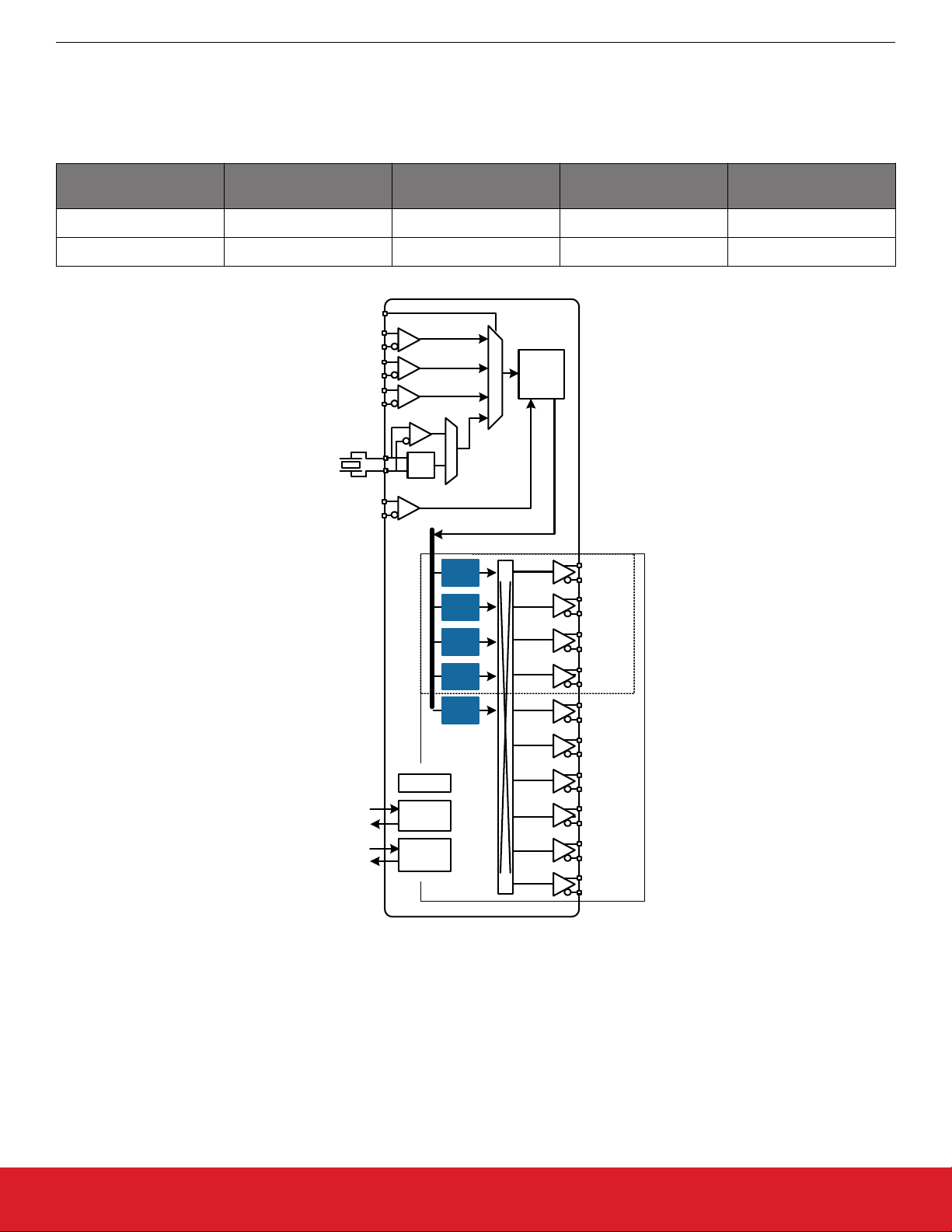
1.2 Family Product Comparison
The following table lists a comparison of the different family members.
Table 1.1. Product Selection Guide
Si5341, Si5340 Rev D Family Reference Manual
Overview
Part Number Number of Inputs
Number of
Fractional Dividers
Number of Outputs Package Type
Si5341 4 5 10 64-pin QFN
Si5340 4 4 4 44-pin QFN
Si5341/40
IN_SEL[1:0]
IN0
XTAL
IN1
IN2
XA
OSC
XB
FB_IN
Multi
Synth
Multi
Synth
Multi
Synth
Multi
Synth
Multi
Synth
PLL
OUT0
OUT1
OUT2
OUT3
OUT4
Si5340
OUT5
NVM
I2C/ SPI
Control/
Status
OUT6
OUT7
OUT8
OUT9
Si5341
Figure 1.1. Block Diagram Si5341/40
silabs.com | Building a more connected world. Rev. 1.3 | 6
Page 7

1.3 Available Software Tools and Support
Si5341, Si5340 Rev D Family Reference Manual
Overview
ClockBuilder
Pro is a software tool that is used for the Si5341/40 family and other product families, capable of configuring the timing
chip in an intuitive friendly step by step process. The software abstracts the details from the user to allow focus on the high level input
and output configuration, making it intuitive to understand and configure for the end application. The software walks the user through
each step, with explanations about each configuration step in the process to explain the different options available. The software will
restrict the user from entering an invalid combination of selections. The final configuration settings can be saved, written to a device or
written to the EVB and a custom part number can be created. ClockBuilder Pro integrates all the datasheets, application notes and
information that might be helpful in one environment. It is intended that customers will use the software tool for the proper configuration
of the device. Register map descriptions are given in the document should not be the only source of information for programming the
device. The complexity of the algorithms is embedded in the software tool.
silabs.com | Building a more connected world. Rev. 1.3 | 7
Page 8

Si5341, Si5340 Rev D Family Reference Manual
Functional Description
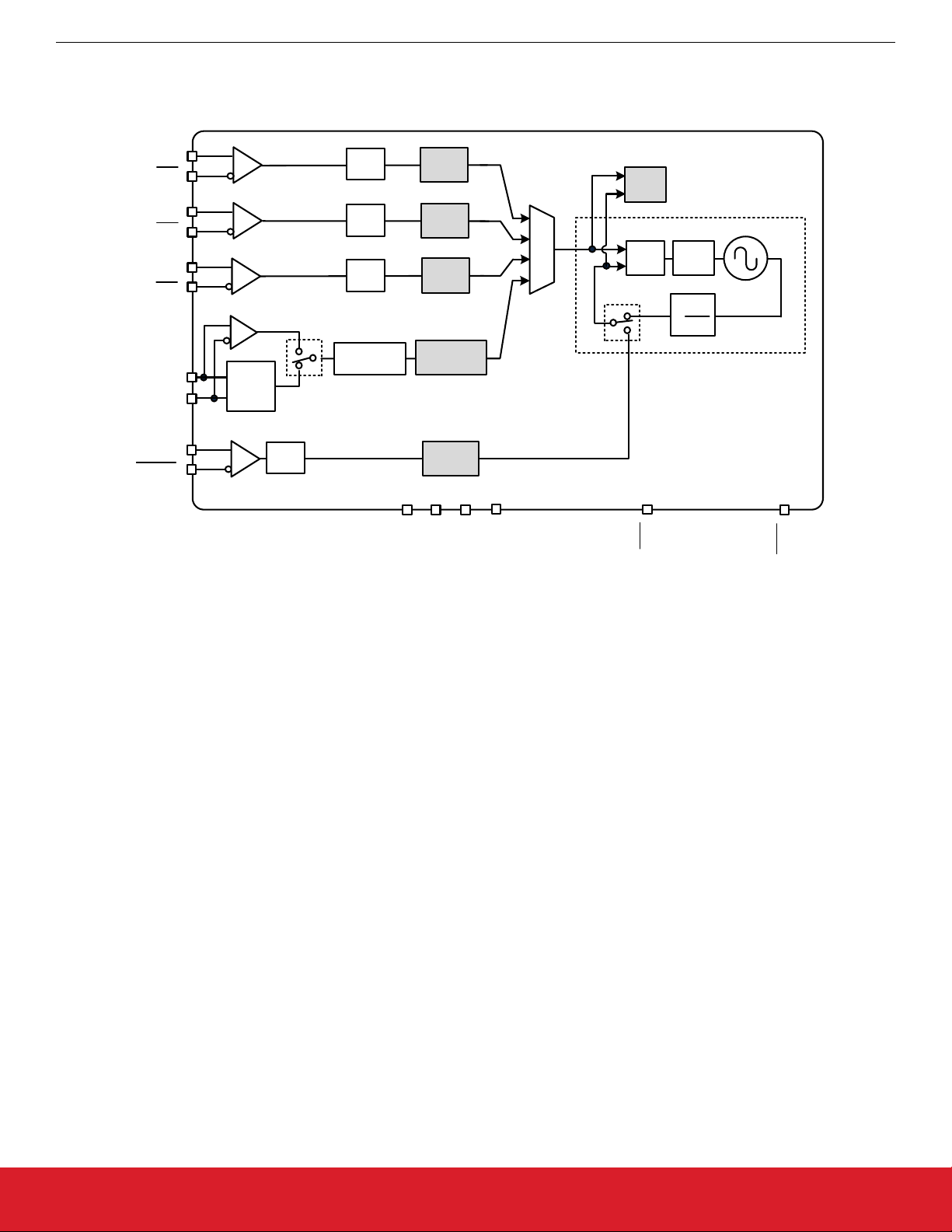
2. Functional Description
The Si5341/40 uses next generation MultiSynth™ technology to offer the industry’s most frequency-flexible, high performance clock
generator. The PLL locks to either an external crystal (XA/XB) or to an external input on XAXB, IN0, IN1 or IN2. The input frequency
(crystal or external input) is multiplied by the DSPLL and divided by the MultiSynth™ stage (N divider) and R divider to any frequency in
the range of 100 Hz to 712.5 MHz per output. The phase-locked loop is fully contained and does not require external loop filter components to operate. Its function is to phase lock to the selected input and provide a common reference to all the output MultiSynth highperformance fractional dividers (N). The high-resolution fractional MultiSynth™ dividers enables true any-frequency input to any-frequency on any of the outputs. A crosspoint mux connects any of the MultiSynth divided frequencies to any of the outputs drivers. Additional output integer dividers (R) provide further frequency division if required. The frequency configuration of the device is programmed
by setting the input dividers (P), the DSPLL feedback fractional divider (M_NUM/M_DEN), the MultiSynth fractional dividers (N_NUM/
N_DEN), and the output integer dividers (R). Silicon Labs’ Clockbuilder Pro configuration utility determines the optimum divider values
for any desired input and output frequency plan.
The output drivers offer flexible output formats which are independently configurable on each of the outputs. This clock generator is fully
configurable via its serial interface (I2C/SPI) and includes in-circuit programmable non-volatile memory. The block diagram for the
Si5341 is shown in Figure 2.1 Si5341 Detailed Block Diagram on page 10, and the block diagram for the Si5340 is shown in Figure
2.2 Si5340 Detailed Block Diagram on page 11.
silabs.com | Building a more connected world. Rev. 1.3 | 8
Page 9

Si5341, Si5340 Rev D Family Reference Manual
Functional Description
2.1 Dividers
are five divider classes within the Si5341/40. See Figure 2.2 Si5340 Detailed Block Diagram on page 11 for a block diagram
There
that shows all of these dividers.
• 1. Wide range input dividers Pfb, P2, P1, P0
• Only integer divider values
• Range is from 1 to 216 – 1
• Since the input to the phase detector needs to be
Each divider has an update bit that must be written to cause a newly written divider value to take effect.
•
2. Narrow range input divider Pxaxb
• Only divides by 1, 2, 4, 8
3. Feedback M divider
• Ultra low jitter in fractional and integer modes
• MultiSynth divider
• Integer or fractional divide values
• 44 bit numerator, 32 bit denominator
• Practical range limited by phase detector range of 10–120 MHz and VCO range of 13500–14256 MHz
• This divider has an update bit that must be written to cause a newly written divider value to take effect.
4. Output N dividers
• Ultra low jitter in fractional and integer modes
• MultiSynth divider
• Integer or fractional divide values
• 44 bit numerator, 32 bit denominator
• Min value is 10
• Maximum value is 212 – 1
• Each N divider has an update bit that must be written to cause a newly written divider value to take effect. In addition there is
a global update bit that when written updates all N dividers.
5. Output R divider
• Only even integer divide values
• Min value is 2
• Maximum value is 225 – 2
> 10 MHz, the practical range is limited to ~75 on the high side.
Additionally, FSTEPW can be used to adjust the nominal output frequency in DCO mode. See Section 6. Digitally Controlled Oscilla-
tor (DCO) Modes for more information and block diagrams on DCO mode.
silabs.com | Building a more connected world. Rev. 1.3 | 9
Page 10
Si5341, Si5340 Rev D Family Reference Manual
Functional Description
VDDA
VDD
3
IN_SEL[1:0]
IN0
IN0
IN1
IN1
IN2
IN2
25MHz, 48-
54MHz
XTAL
FB_IN
FB_IN
I2C_SEL
SDA/SDIO
A1/SDO
SCLK
A0/CS
XB
XA
OSC
SPI/
2
C
I
Zero Delay
Mode
÷P
NVM
÷P
0
÷P
1
÷P
2
÷Pxaxb
fb
Status
Monitors
Si5341
Clock
Generator
PLL
PD
LPF
M
n
÷
M
d
MultiSynth
N
0n
÷
N
0d
N
1n
÷
N
1d
N
2n
÷
N
2d
N
3n
÷
N
3d
N
4n
÷
N
4d
Frequency
Control
Dividers/
Drivers
VDDO0
÷R
0
÷R
1
÷R
2
÷R
3
÷R
4
t
0
÷R
5
t
1
÷R
6
t
2
÷R
7
t
3
÷R
8
t
4
÷R
9
OUT0
OUT0
VDDO1
OUT1
OUT1
VDDO2
OUT2
OUT2
VDDO3
OUT3
OUT3
VDDO4
OUT4
OUT4
VDDO5
OUT5
OUT5
VDDO6
OUT6
OUT6
VDDO7
OUT7
OUT7
VDDO8
OUT8
OUT8
VDDO9
OUT9
OUT9
RST
LOL
INTR
FINC
FDEC
SYNC
OE
Figure 2.1. Si5341 Detailed Block Diagram
silabs.com | Building a more connected world. Rev. 1.3 | 10
Page 11
25MHz, 48-
54MHz
AL
XT
IN0
IN0
IN1
IN1
IN2
IN2
IN_SEL[1:0]
Si5341, Si5340 Rev D Family Reference Manual
Functional Description
Si5340
XA
OSC
XB
Zero Delay
Mode
÷Pxaxb
÷P
0
÷P
1
÷P
2
Clock
Generator
PLL
LPF
PD
MultiSynth
N
0n
÷
÷
M
d
÷
M
n
÷
÷
t
N
N
N
N
N
N
N
0
0d
1n
t
1
1d
2n
t
2
2d
3n
t
3
3d
Dividers/
Drivers
÷R
0
÷R
1
÷R
2
÷R
3
VDDO0
OUT0
OUT0
VDDO1
OUT1
OUT1
VDDO2
OUT2
OUT2
VDDO3
OUT3
OUT3
FB_IN
FB_IN
÷P
fb
Status
Monitors
3
RST
VDD
VDDA
LOL
INTR
LOSXAB
SPI/
I2C_SEL
SDA/SDIO
2
C
I
A1/SDO
SCLK
NVM
OE
A0/CS
Figure 2.2. Si5340 Detailed Block Diagram
silabs.com | Building a more connected world. Rev. 1.3 | 11
Page 12
3. Powerup and Initialization
The following figure shows the powerup and initialization sequence.
Si5341, Si5340 Rev D Family Reference Manual
Powerup and Initialization
Power-Up
Hard Reset
bit asserted
RST
pin asserted
NVM download
Soft Reset
bit asserted
Initialization
Serial interface
ready
Figure 3.1. Power-Up and Initialization
3.1 Reset and Initialization
power is applied, the device begins an initialization period where it downloads default register values and configuration data from
Once
NVM and performs other initialization tasks. Communicating with the device through the serial interface is possible once this initialization period is complete. No clocks will be generated until the initialization is done. There are two types of resets available. A hard reset
is functionally similar to a device power-up. All registers will be restored to the values stored in NVM, and all circuits will be restored to
their initial state including the serial interface. A hard reset is initiated using the RSTb pin or by asserting the hard reset bit. A soft reset
bypasses the NVM download. It is simply used to initiate register configuration changes.
Table 3.1. Reset Registers
Register Name
HARD_RST 001E[1] 001E[1]
SOFT_RST 001C[0] 001C[0]
The Si541/40 is fully configurable using the serial interface (I2C
from internal non-volatile memory (NVM). Application specific default configurations can be written into NVM allowing the device to generate specific clock frequencies at power-up. Writing default values to NVM is in-circuit programmable with normal operating power supply voltages applied to its VDD (1.8 V) and VDDA (3.3 V) pins.
3.1.1 Power Supply Sequencing
If the output clocks do not need to have a specific phase/delay relationship between them the timing of the power supplies coming up to
full voltage is irrelevant. However, if the phase/delay of any output clock to any other output clock is important, then the VDDO of the
relevant clock output must come up to full voltage before VDD and VDDA voltages are applied. See . Voltage can always be applied to
the VDDS pin regardless of any output clock alignment.
Hex Address [Bit Field]
Function
Si5341 Si5340
Performs the same function as power cycling the device. All registers will be restored to their default values.
Performs a soft reset. Resets the device while it does not redownload the register configuration from NVM.
or SPI). At power up the device downloads its default register values
silabs.com | Building a more connected world. Rev. 1.3 | 12
Page 13
3.2 NVM Programming
Si5341, Si5340 Rev D Family Reference Manual
Powerup and Initialization
Devices
have two categories of non-volatile memory: user NVM and Factory (Silabs) NVM. Each type is segmented into NVM banks.
There are three NVM banks, one of which is used for factory programming (whether a base part or an Orderable Part Number). Two
user NVM banks remain; therefore, the device NVM can be re-burned in the field up to two times. Factory NVM cannot be modified, and
contains fixed configuration information for the device.
The ACTIVE_NVM_BANK device setting can be used to determine which user NVM bank is currently being used and therefore how
many banks, if any, are available to burn. The following table describes possible values:
Table 3.2. NVM Bank Burning Values
Active NVM BANK Value (Deci-
Number of User Banks Burned Number of User Banks Available to Burn
mal)
3 (factory state) 1 2
15 2 1
63 3 0
Note: While polling DEVICE_READY during the procedure below, the following conditions must be met to ensure the correct values are
written into the NVM:
VDD and VDDA power must both be stable throughout the process.
•
• No additional registers may be written or read during DEVICE_READY polling. This includes the PAGE register at address 0x01.
DEVICE_READY is available on every register page, so no page change is needed to read it.
• Only the DEVICE_READY register (0xFE) should be read during this time.
The procedure for writing registers into NVM is as follows:
1. Write registers as needed for desired device operation. Verify device operation to ensure the device is configured correctly before
preceeding. Do not skip this important step.
2. You may write to the user scratch space (Registers 0x026B to 0x0272 DESIGN_ID0-DESIGN_ID7) to identify the contents of the
NVM bank.
3. Write 0xC7 to NVM_WRITE register. This starts the internal NVM burn sequence, writing NVM from the internal registers. Do not
access ANY other registers than DEVICE_READY during the NVM burn process. Doing so may corrupt the NVM burn in progress.
4. Poll DEVICE_READY until DEVICE_READY=0x0F (waiting for completion of NVM burn sequence).
5. Set NVM_READ_BANK 0x00E4[0]=1. This will download the NVM contents back into non-volatile memory (registers).
6. Poll DEVICE_READY until DEVICE_READY=0x0F (waiting for NVM download to complete).
7. Read ACTIVE_NVM_BANK and verify that the value is the next highest value in the table above. For example, from the factory it
will be a 3. After NVM_WRITE, the value will be 15.
Alternatively, steps 5 and 6 can be replaced with a Hard Reset, either by RSTb pin, HARD_RST register bit, or power cycling the device
to generate a POR. All of these actions will load the new NVM contents back into the device registers.
The ClockBuilder Pro Field Programmer kit is a USB attached device to program supported devices either in-system (wired to your
PCB) or in-socket (by purchasing the appropriate field programmer socket). ClockBuilder Pro software is then used to burn a device
configuration (project file). Learn more at https://www.silabs.com/products/development-tools/timing/cbprogrammer.
Table 3.3. NVM Programming Registers
Register Name Hex Address
Function
[Bit Field]
ACTIVE_NVM_BANK 0x00E2[7:0] Identifies the active NVM bank.
NVM_WRITE 0x00E3[7:0] Initiates an NVM write when written with value 0xC7.
NVM_READ_BANK 0x00E4[0] Download register values with content stored in NVM.
DEVICE_READY 0x00FE[7:0] Indicates that the device is ready to accept commands when
value = 0x0F.
silabs.com | Building a more connected world. Rev. 1.3 | 13
Page 14

Si5341, Si5340 Rev D Family Reference Manual
Powerup and Initialization
Warning:
Any attempt to read or write any register other than DEVICE_READY before DEVICE_READY reads as 0x0F may corrupt
the NVM programming and may corrupt the register contents, as they are read from NVM. Note that this includes accesses to the
PAGE register.
silabs.com | Building a more connected world. Rev. 1.3 | 14
Page 15

Si5341, Si5340 Rev D Family Reference Manual
Clock Inputs
4. Clock Inputs
The PLL in the Si5341/40 requires a clock at the XAXB or IN2, 1, 0 input pins or a clock from a crystal connected across the XAXB
pins.
4.1 Inputs on XA/XB
4.1.1 Crystal on XA/XB
An external standard crystal (XTAL) is connected to XA/XB when this input is configured as a crystal oscillator. A crystal frequency of
25 MHz can be used although crystals in the frequency range of 48 MHz to 54 MHz are recommended for the best jitter performance.
Recommended crystals are listed below. The Si5341/40 includes a built-in XTAL load capacitance (CL) of 8 pF, but crystals with CL
specifications as high as 18 pF can also be used. When using crystals with CL specs higher than 8 pf it is not generally recommended
to use external capacitors from XA/XB to ground to increase the crystal load capacitance. Rather the frequency offset due to CL mis-
match can be adjusted using the XAXB_FREQ_OFFSET word which allows frequency adjustments of up to ±1000 ppm. See 11. Crys-
tal and Device Circuit Layout Recommendations for the PCB layout guidelines.
silabs.com | Building a more connected world. Rev. 1.3 | 15
Page 16
Si5341, Si5340 Rev D Family Reference Manual
Clock Inputs
4.1.2 Clock Input on XA/XB
external clock can also be input on the XA/XB pins. Selection between the external crystal or clock is controlled by register configu-
An
ration. The internal crystal load capacitors (CL) are disabled in external clock mode. Because the input buffer at XA/XB is a lower noise
buffer than the buffers on IN2,1,0, a very clean input clock at XA/XB, such as a very high quality TCXO or XO, will, in some cases,
produce lower output clock jitter than the same input at IN2,1,0. If the XAXB input is unused and powered down then the XA and XB
inputs can be left floating. Note that ClockBuilder Pro will power down the XAXB input if it is selected as “unused”. If XAXB is powered
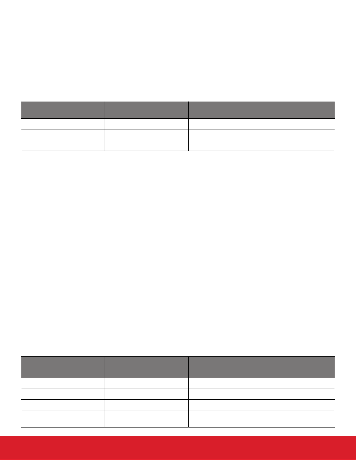
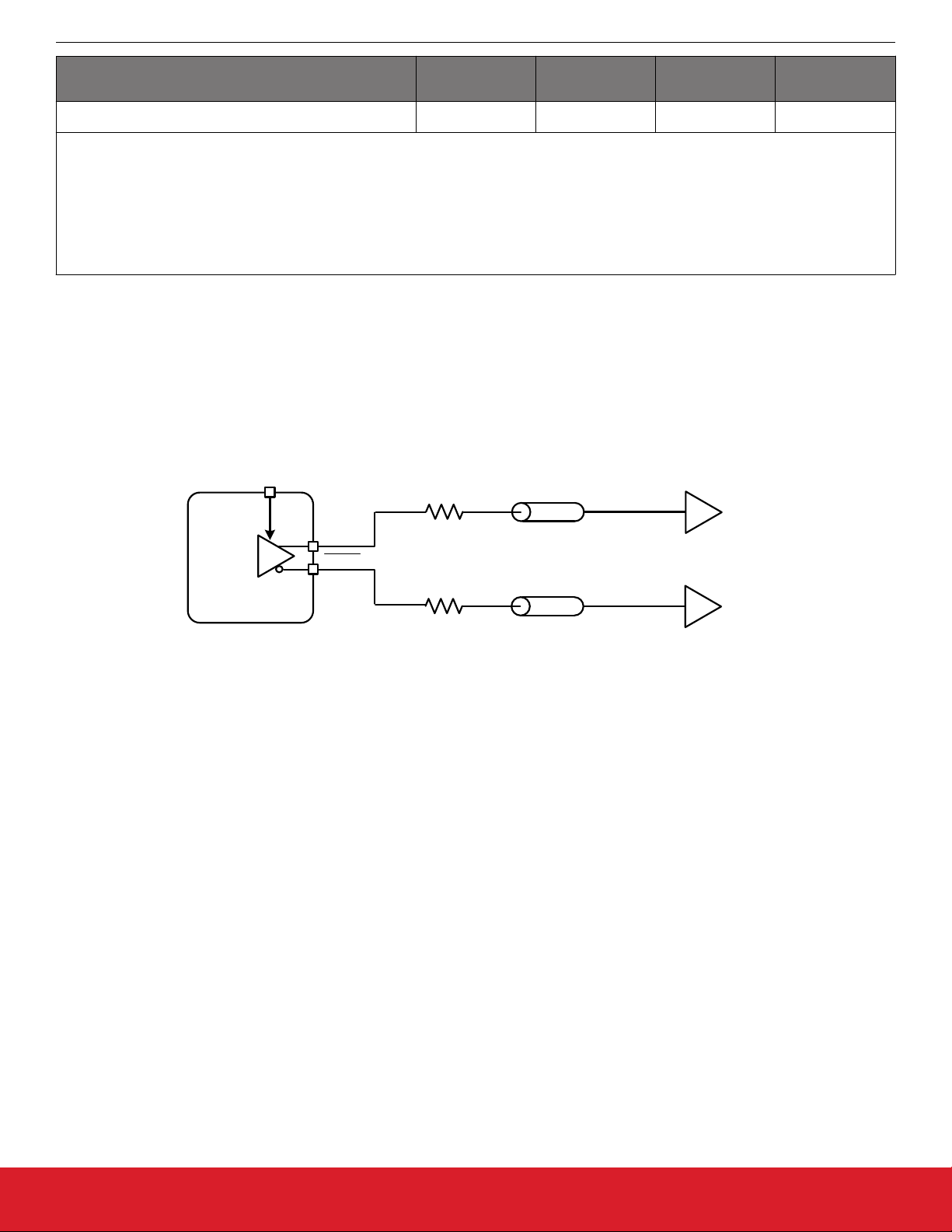
up but no input is applied then the XA input should be left floating and the XB input must be connected directly to ground. Both a singleended or a differential clock can be connected to the XA/XB pins as shown in the following figure:
Differential Connection
0.1 µf
0.1 µf
Note: 2.5 Vpp diff max
CMOS/XO
Output
XO VDD R1 R2
3.3 V 523 Ohms
475 Ohms
2.5 V
1.8 V
158 Ohms
422 Ohms
649 Ohms
866 Ohms
X1
nc
X2
nc
2xC
50
XA
OSC
XB
50
2xC
Single-ended Connection
Note: 2.0 Vpp_se max
R1
R2
0.1 µf
0.1 µf
L
L
0.1 µf
Si5341/40
X1
nc
X2
nc
XA
XB
2xC
2xC
L
OSC
L
Single-ended XO Connection
Note: 2.0 Vpp_se max
XO with Clipped Sine
Wave Output
Si5341/40
X1
nc
X2
nc
2xC
0.1 µf
XA
XB
0.1 µf
2xC
Crystal Connection
X1
XA
XTA
L
XB
X2
2xCL
2xC
L
OSC
L
OSC
L
Si5341/40
Si5341/40
Figure 4.1. Crystal Resonator and External Reference Clock Connection Options
In addition to crystal operations, a clipped sine wave, CMOS, or differential reference clock is also accepted on the XA/XB interface.
clipped sine wave and CMOS TCXOs have insufficient drive strength to drive a 100 Ω or 50 Ω load. For this reason, place the
Most
TCXO as close to the Si5340/41 as possible to minimize PCB trace length. In addition, ensure that both the Si5340/41 and the TCXO
are both connected directly to the ground plane. The above figure includes the recommended method of connecting a clipped sine
wave TCXO to the Si5340/41. Because the Si5340/41 provides DC bias at the XA and XB pins, the ~800 mV peak-peak swing can be
input directly into the XA interface of the Si5340/41 once it has been ac-coupled.
The above figure also illustrates the recommended method of connecting a CMOS rail-to-rail output to the XA/XB inputs. Because the
signal is single-ended, the XB input is ac-coupled to ground. The resistor network attenuates the rail-to-rail output swing to ensure that
the maximum input voltage swing at the XA pin is less than the data sheet specification. The signal is ac-coupled before connecting it to
the Si5340/41 XA input. Again, since the signal is single-ended, the XB input should be ac-coupled to ground.
If an external oscillator is used as the XAXB reference, it is important to use a low jitter source because there is effectively no jitter
attenuation from the XAXB pins to the outputs. To minimize jitter at the XA/XB pins, the rise time of the XA/XB signals should be as fast
as possible.
For best jitter performance, use a XAXB frequency above 40 MHz. Also, for XAXB frequencies higher than 125 MHz, the PXAXB control must be used to divide the input frequency down below 125 MHz.
In most applications, using the internal OSC with an external crystal provides the best phase noise performance. See AN905: External
References; Optimizing Performance for more information on the performance of various XO's with these devices.
silabs.com | Building a more connected world. Rev. 1.3 | 16
Page 17
Si5341, Si5340 Rev D Family Reference Manual
Clock Inputs
The recommended crystal and oscillator suppliers are listed in the Si534x/8x
XOs Reference Manual.
4.2 Clock Inputs on IN2, IN1, IN0
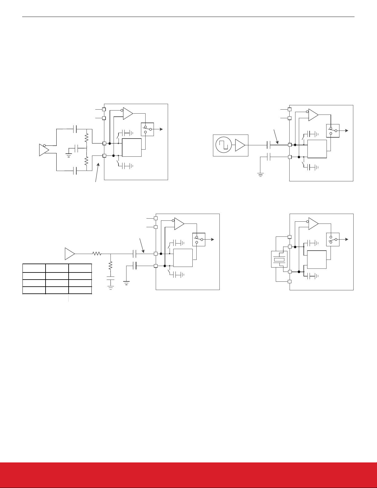
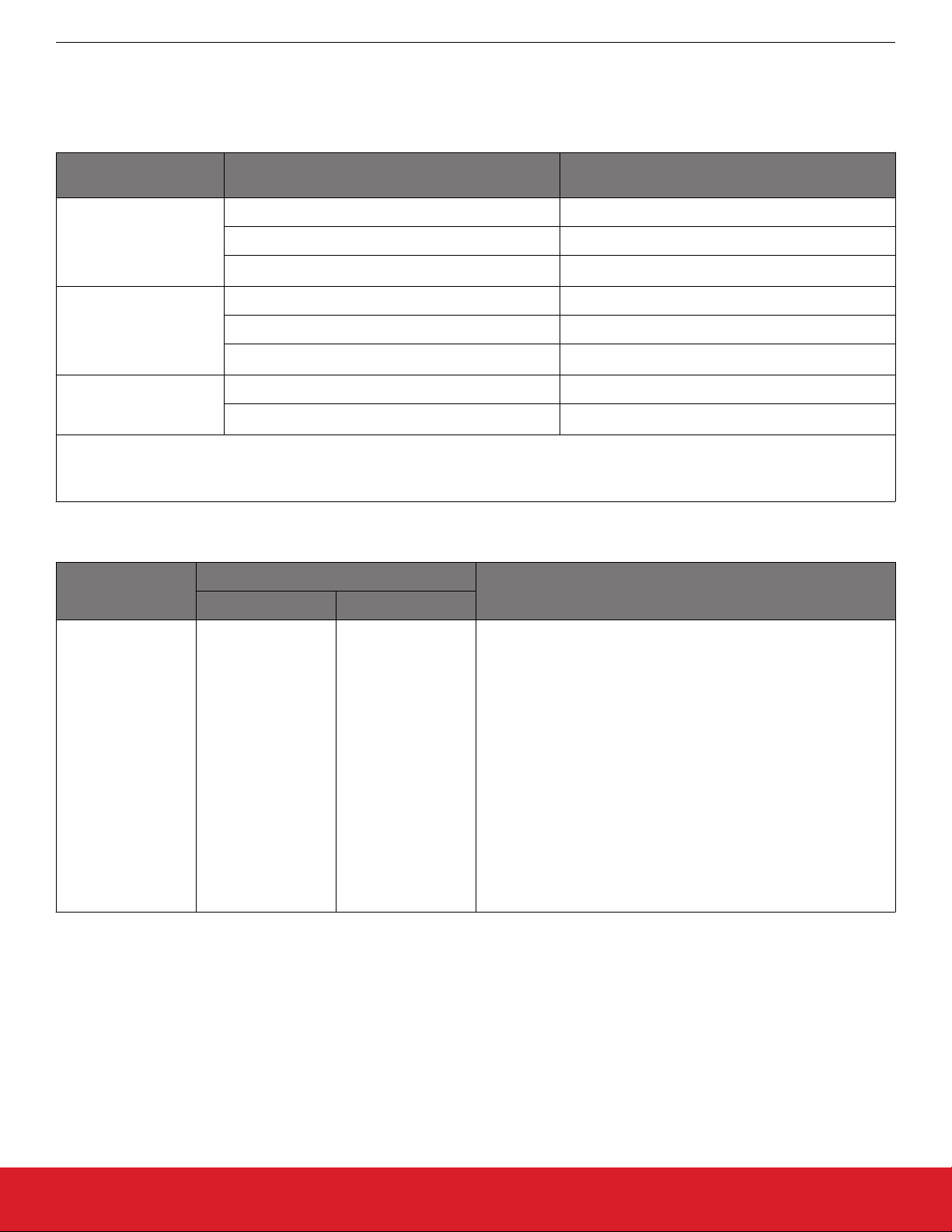
A single ended or differential clock may be input to the IN2, 1, 0 inputs as shown below. All input signals must be ac-coupled. When INx
(x = 0, 1, 2) is unused and powered down the plus and minus input can be left floating. ClockBuilder Pro will power down any INx input
that is selected as “unused.” If any INx is powered up but does not have any input signal then the plus input should be left floating and
the minus input should be directly connected to ground. If the plus input is left floating and the minus input is connected to ground with a
4.7 kΩ or smaller resistor, then the INx can be powered up or down when it does not have an input. The recommended input termination schemes are shown in the figure below. Unused inputs can be disabled by register configuration.
Jitter Attenuators Recommended Crystal, TCXO and OC-
Standard AC-Coupled Differential
0.1uF *
50
INx
100
Standard
INxb
50
LVDS, LVPECL, CML
0.1uF *
* These caps should have < ~5 ohms capacitive reactance at the clock input frequency.
Clock IC
Standard AC-Coupled Single-Ended
C1
RS
50
3.3V, 2.5V, 1.8V LVCMOS
RS matches the CMOS driver to a
50 ohm transmission
line (if used)
R1
R
2
0.1uF
0.1uF
INx
INxb
Standard
0.1uF *
**
*This cap should have less than ~20 ohms of capacitive reactance at the clock input
frequency.
** Only when 3.3V LVCMOS driver is present, use R2 = 845 ohm and R1 = 267 ohm if
needed to keep the signal at INx < 3.6 Vpp_se. Including C1 = 6 pf may improve the
output jitter due to faster input slew rate at INx. If attenuation is not needed for
Inx<3.6Vppse, make R1 = 0 ohm and omit C1, R2 and the capacitor below R2. C1, R1,
and R2 should be physically placed as close as practicle to the device input pins.
Figure 4.2. Terminations for Differential and Single-Ended Inputs
Clock IC
4.3 Unused Inputs
Unused
used input bits will disable them. Enabled inputs not actively being driven by a clock may benefit from pull up or pull down resistors to
avoid them responding to system noise.
silabs.com | Building a more connected world. Rev. 1.3 | 17
inputs can be disabled and left unconnected. Register 0x0949[3:0] defaults the input clocks to being enabled. Clearing the un-
Page 18
Si5341, Si5340 Rev D Family Reference Manual
Clock Inputs
4.4 Reference Input Selection (IN0, IN1, IN2, XA/XB)
active clock input is selected using the IN_SEL1,0 pins or by register control. The register bit IN_SEL_REGCTRL determines input
The
selection as pin or register selectable. If the selected input does not have a clock, all output clocks will be shut off.
Table 4.1. Manual Input Selection Using IN_SEL[1:0] Pins
IN_SEL[1:0] Selected Input
0 0 IN0
0 1 IN1
1 0 IN2
1 1 XA/XB
Table 4.2. Input Control Registers
Register Name
Function
Si5341 Si5340
Adjusts for crystal load capacitance mismatch causing oscillation
frequency errors up to ±1000 ppm. This word is in 2s complement
Hex Address [Bit Field]
XAXB_FREQ_OFFSET 0202[7:0]–0205[7:0]
format.
The XAXB_FREQ_OFFSET word is added to the M divider numerator.
Selects between the XTAL or external reference clock on the
XAXB_EXTCLK_EN 090E[0]
XA/XB pins. Default is 0, XTAL. Set to 1 to use an external reference oscillator
IN_SEL_REGCTRL 0021[0] Determines pin or register clock input selection.
IN_SEL 0021[2:1] Selects the input when in register input selection mode.
IN_EN 0949[3:0]
Allows enabling/disabling IN0, IN1, IN2 and FB_IN when not in
use.
Table 4.3. XAXB Pre-Scale Divide Ratio Register
Setting Name Hex Address [Bit Field] Function
PXAXB 0x0206[1:0] Sets the XAXB input divider value according to the table be-
low.
The following table lists the values, along with the corresponding divider ratio.
Table 4.4. XAXB Pre-Scale Divide Values
Value (Decimal) PXAXB Divider Value
0 1
1 2
2 4
3 8
silabs.com | Building a more connected world. Rev. 1.3 | 18
Page 19
Si5341, Si5340 Rev D Family Reference Manual
Clock Inputs
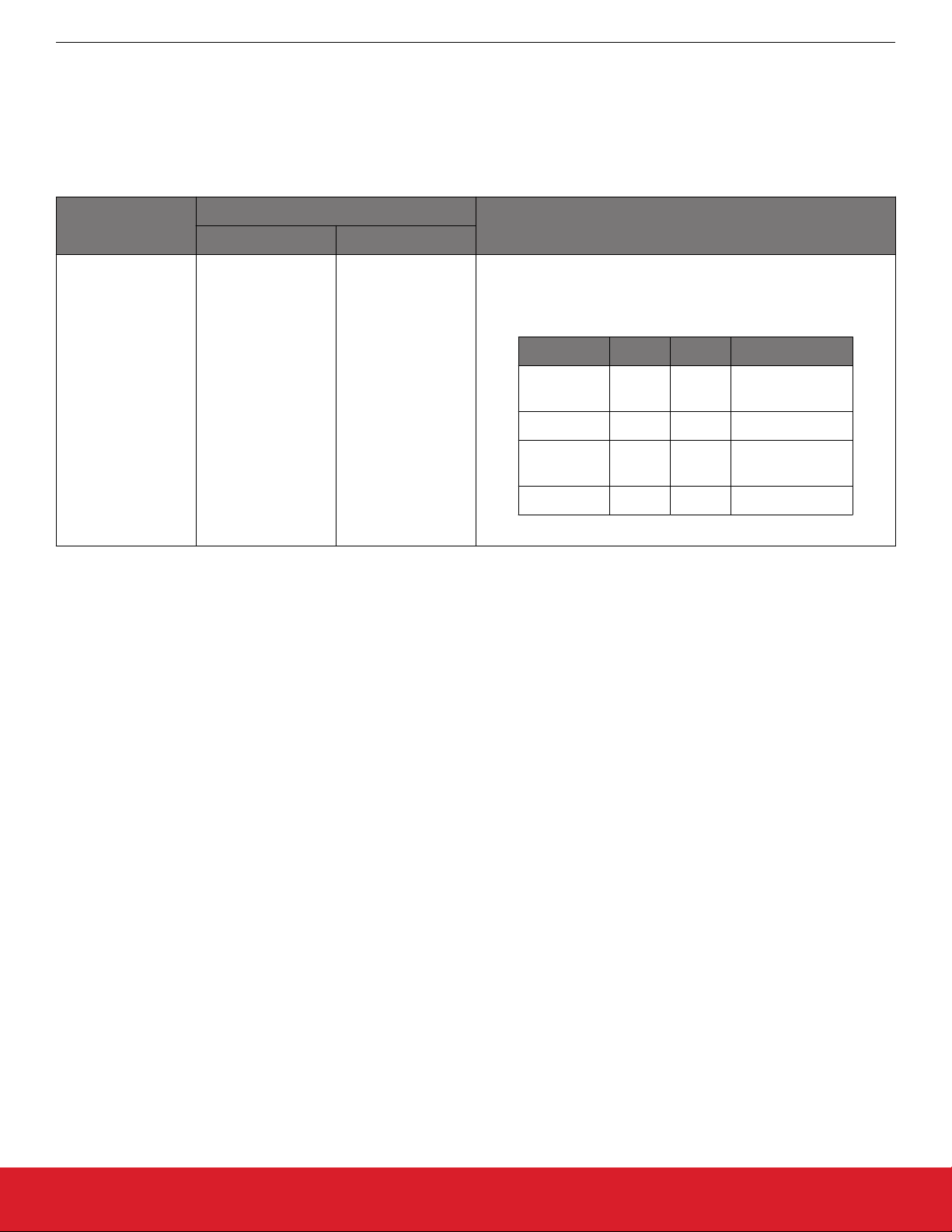
4.5 Fault Monitoring
Si5341/40 provides fault indicators which monitor loss of signal (LOS) of the inputs (IN0, IN1, IN2, XA/XB, FB_IN) and loss of lock
The
(LOL) for the PLL. This is shown in the following figure.
IN0
IN0
IN1
IN1
IN2
IN2
XA
XB
FB_IN
FB_IN
OSC
÷P
÷P
÷P
0
1
LOS0
LOL
LOS1
Si5341/40
PLL
LPFPD
÷P
2
÷Pxaxb
fb
LOS2
LOSXAXB
LOS0
LOSFB
LOS1
LOS2
LOSXAB
LOL
÷
Mn
Md
INTR
Figure 4.3. LOS and LOL Fault Monitors
silabs.com | Building a more connected world. Rev. 1.3 | 19
Page 20

Si5341, Si5340 Rev D Family Reference Manual
Clock Inputs
4.5.1 Status Indicators
state of the status monitors are accessible by reading registers through the serial interface or with dedicated pin (LOLb). Each of
The
the status indicator register bits has a corresponding sticky bit (_FLG) in a separate register location. Once a status bit is asserted its
corresponding _FLG bit will remain asserted until cleared. Writing a logic zero to a _FLG register bit clears its state.
Table 4.5. Status Monitor Bits (Si5341 and Si5340)
Setting Name Hex Address [Bit Field] Function
Status Register Bits
SYSINCAL 0x000C[0] Asserted when in calibration.
LOSXAXB 0x000C[1]
Loss of Signal at the XA input.
The XB input does not have an LOS detector.
LOSREF 0x000C[2] Loss of Signal for the input that has been selected.
LOL 0x000C[3] Loss of Lock for the PLL.
SMBUS_TIMEOUT 0x000C[5] The SMB bus has a timeout.
LOSIN[3:0] 0x000D[3:0] Loss of Signal for the FB_IN, IN2, IN1, IN0 inputs.
Sticky Status Register Bits
SYSINCAL_FLG 0x0011[0] Sticky bit for SYSINCAL
LOSXAXB_FLG 0x0011[1] Sticky bit for LOSXAXB
LOSREF_FLG 0x0011[2] Sticky bit for LOSREF
LOL_FLG 0x0011[3] Sticky bit for LOL
SMBUS_TIMEOUT_FLG 0x0011[5] Sticky bit for SMBUS_TIMEOUT
LOSIN_FLG 0x0012[3:0] Sticky bit for FB_IN, IN2, IN1, IN0
silabs.com | Building a more connected world. Rev. 1.3 | 20
Page 21
Si5341, Si5340 Rev D Family Reference Manual
Clock Inputs
4.5.2 Interrupt Pin (INTRb)
interrupt pin (INTRb) is asserted (low) whenever any of the unmasked _FLG bits are asserted. All _FLG bits are maskable to pre-
An
vent assertion of the interrupt pin. The state of the INTRb pin is reset by writing zeros to all _FLG bits that are set or by writing a 1 to
mask all _FLG bits that are set.
Table 4.6. Interrupt Mask Bits
Setting Name
Function
Si5341 and Si5342
SYSINCAL_INTR_MSK 0x0017[0] 1 = SYSINCAL_FLG is prevented from asserting the INTR pin
LOSXAXB_INTR_MSK 0x0017[1] 1 = LOSXAXB_FLG is prevented from asserting the INTR pin
LOSREF_INTR_MSK 0x0017[2] 1 = LOSREF_FLG is prevented from asserting the INTR pin
LOL_INTR_MSK 0x0017[3] 1 = LOL_FLG is prevented from asserting the INTR pin
SMB_TMOUT_INTR_MSK 0x0017[5] 1 = SMBUS_TIMEOUT_FLG is prevented from asserting the INTR pin
LOSIN _INTR_MSK[3:0] 0x0018[3:0] 1 = LOS_FLG is prevented from asserting the INTR pin
mask
LOSIN_FLG[0]
mask
LOSIN_FLG[1]
mask
LOSIN_FLG[2]
Hex Address [Bit Field]
mask
LOSIN_FLG[3]
INTRb
LOSXAXB_FLG
LOL_FLG
mask
mask
Figure 4.4. Interrupt Flags and Masks
silabs.com | Building a more connected world. Rev. 1.3 | 21
Page 22

Si5341, Si5340 Rev D Family Reference Manual
Output Clocks
5. Output Clocks
5.1 Outputs
The Si5341 supports ten differential output drivers which can be independently configured as differential or LVCMOS. The Si5340 supports four output drivers independently configurable as differential or LVCMOS.
5.2 Performance Guidelines for Outputs
Whenever a number of high-frequency, fast-rise-time, large amplitude signals are all close to one another, the laws of physics dictate
that there will be some amount of crosstalk. The jitter of the Si5341/40 is so low that crosstalk can become a significant portion of the
final measured output jitter. Some of the source of the crosstalk will be the Si5341/40, and some will be introduced by the PCB. It is
difficult (and possibly irrelevant) to allocate the jitter portions between these two sources because the jitter can only be measured when
an Si5341/40 is mounted on a PCB.
For extra fine tuning and optimization, in addition to following the usual PCB layout guidelines, crosstalk can be minimized by modifying
the arrangements of different output clocks. For example, consider the following lineup of output clocks in the table below.
Table 5.1. Example of Output Clock Frequency Sequencing Choice
Output
0 155.52 155.52
1 156.25 155.52
2 155.52 622.08
3 156.25 Not used
4 200 156.25
5 100 156.25
6 622.08 625
7 625 Not used
8 Not used 200
9 Not used 100
Using this example, a few guidelines are illustrated:
1. Avoid
2. Adjacent frequency values that are integer multiples of one another are okay and these outputs should be grouped accordingly.
3. Unused outputs can be used to separate clock outputs that might otherwise interfere with one another. In this case, see OUT3 and
adjacent frequency values that are close. A 155.52 MHz clock should not be next to a 156.25 MHz clock. If the jitter integra-
tion bandwidth goes up to 20 MHz, then keep adjacent frequencies at least 20 MHz apart.
Noting that, because 155.52 x 4 = 622.08 and 156.25 x 4 = 625, it is acceptable to place 155.52 MHz close to 622.08 MHz and
156.25 MHz close to 625 MHz.
OUT7.
Not Recommended
(Frequency MHz)
Recommended
(Frequency MHz)
If some outputs have tight jitter requirements while others are relatively loose, rearrange the clock outputs so that the critical outputs are
the least susceptible to crosstalk. These guidelines typically only need to be followed by those applications that wish to achieve the
highest possible levels of jitter performance. Because CMOS outputs have large pk-pk swings and do not present a balanced load to
the VDDO supplies, CMOS outputs generate much more crosstalk than differential outputs. For this reason, CMOS outputs should be
avoided whenever possible. When CMOS is unavoidable, even greater care must be taken with respect to the above guidelines. It is
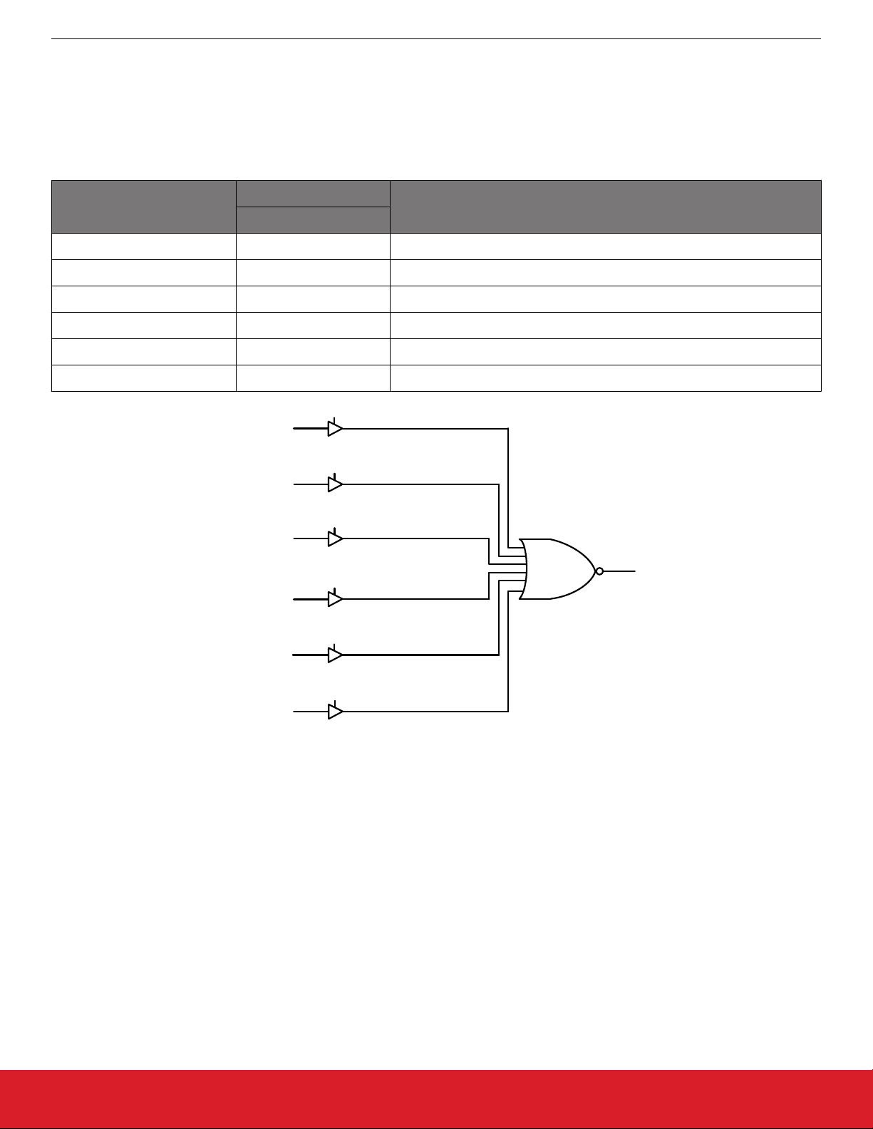
highly recommended that you consult AN862: Optimizing Si534x Jitter Performance in Next Generation Internet Infrastructure Systems.
The ClockBuilder Pro Clock Placement Wizard is an easy way to reduce crosstalk for a given frequency plan. This feature can be accessed on the “Define Output Clocks” page of ClockBuilder Pro in the lower left hand corner of the page. It is recommended to use this
tool after each project frequency plan change.
silabs.com | Building a more connected world. Rev. 1.3 | 22
Page 23

Si5341, Si5340 Rev D Family Reference Manual
Output Clocks
5.3 Output Signal Format
differential amplitude is fully programmable covering a wide variety of signal formats including LVDS, LVPECL, HCSL. For CML or
The
non-standard amplitude applications, see XREF Appendix A. The common-mode voltage must be set as required for LVDS or LVPECL
or CML/non-standard amplitude levels. The differential formats can be either normal or low power. Low power format uses less power
for the same amplitude but has the drawback of slower rise/fall times. The source impedance in low power format is much higher than
100 ohms. See XREF Appendix A for register settings to implement variable amplitude differential outputs. In addition to supporting
differential signals, any of the outputs can be configured as LVCMOS (3.3, 2.5, or 1.8 V) drivers providing up to 20 single-ended outputs, or any combination of differential and single-ended outputs. Note also that CMOS output can create much more crosstalk than
differential outputs so extra care must be taken in their pin replacement so that other clocks that need the lowest jitter are not on nearby
pins. See AN862: Optimizing Si534x Jitter Performance in Next Generation Internet Infrastructure Systems for additional information.
Table 5.2. Output Signal Format Control Registers
Setting Name
OUT0_FORMAT
OUT1_FORMAT
OUT2_FORMAT
OUT3_FORMAT
OUT4_FORMAT
OUT5_FORMAT
OUT6_FORMAT
OUT7_FORMAT
OUT8_FORMAT
OUT9_FORMAT
Hex Address [Bit Field]
Si5341 Si5340
0109[2:0]
010E[2:0]
0113[2:0]
0118[2:0]
011D[2:0]
0122[2:0]
0127[2:0]
012C[2:0]
0131[2:0]
013B[2:0]
0113[2:0]
0118[2:0]
0127[2:0]
012C[2:0]
—
—
—
—
—
—
Function
Selects the output signal format as normal differential, low power
differential, in phase CMOS, or complementary CMOS.
silabs.com | Building a more connected world. Rev. 1.3 | 23
Page 24
Si5341, Si5340 Rev D Family Reference Manual
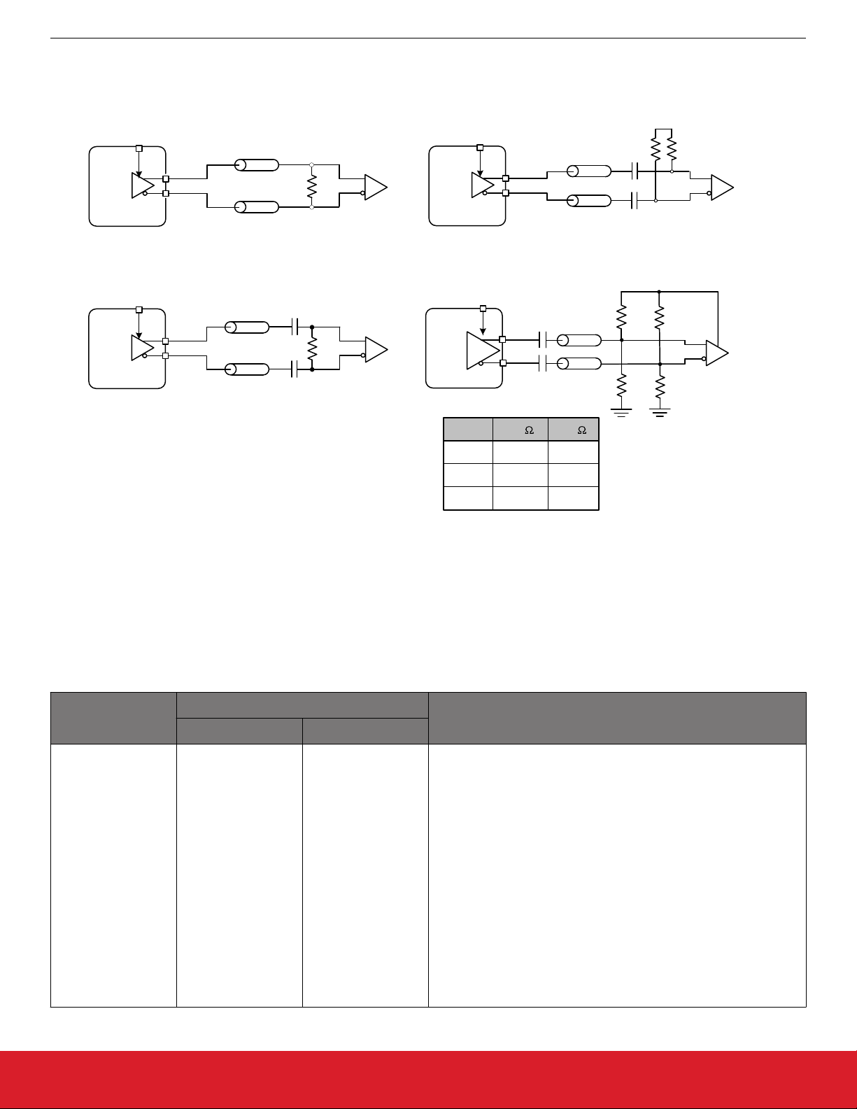
5.3.1 Differential Output Terminations
The differential output drivers support both ac-coupled and dc-coupled terminations as shown in the figure below.
AC Coupled CMLDC Coupled LVDS
LVDS: V
= 3.3V, 2.5V, 1.8V
DDO
OUTx
OUTxb
= 3.3V
, 2.5V
V
DDO
50
100
50
OUTx
OUTxb
50
50
VDD – 1.3V
0.1uF*
0.1uF*
Output Clocks
5050
AC Coupled LVDS/LVPECL
= 3.3V
DDO
, 2.5V, 1.8V
= 3.3V, 2.5V
DDO
OUTx
OUTxb
0.1uF*
50
100
50
0.1uF*
Internally
self-biased
LVDS: V
LVPECL: V
*All caps should have < 5 ohms capacitive reactance at the clock output frequency
= 3.3V, 2.5V. 1.8V
V
DDO
VDD
RX
3.3 V
2.5 V
1.8 V
For V
AC Coupled HCSL
0.1uF*
OUTx
OUTxb
0.1uF*
= 0.35 V
CM
R1 R2
442
332
243
56.2
59.0
63.4
VDD
RX
R1
50
50
R2
R1
Standard
HCSL
R2
Receiver
Figure 5.1. Supported Differential Output Terminations
5.3.2 Differential Amplitude Controls
differential amplitude of each output can be controlled with the following registers. See XREF Appendix A for register settings for
The
non-standard amplitudes.
Table 5.3. Differential Output Voltage Swing (Amplitude) Control Registers
Setting Name
Function
Si5341 Si5340
Hex Address [Bit Field]
OUT0_AMPL
OUT1_AMPL
OUT2_AMPL
OUT3_AMPL
OUT4_AMPL
OUT5_AMPL
OUT6_AMPL
OUT7_AMPL
OUT8_AMPL
OUT9_AMPL
silabs.com | Building a more connected world. Rev. 1.3 | 24
010A[6:4]
010F[6:4]
0114[6:4]
0119[6:4]
011E[6:4]
0123[6:4]
0128[6:4]
012D[6:4]
0132[6:4]
013C[6:4]
0114[6:4]
0119[6:4]
0128[6:4]
012D[6:4]
—
—
—
—
—
—
Sets the voltage swing (amplitude) for the differential output drivers when in Normal differential format and Low Power differential
format (Table 5.4 Settings for LVDS, LVPECL, and HCSL on page
25).
Page 25
Si5341, Si5340 Rev D Family Reference Manual
Output Clocks
5.3.3 Output Driver Settings for LVPECL, LVDS, HCSL, and CML
Each differential output has four settings for control:
Normal or Low Power Format
1.
2. Amplitude (sometimes called Swing)
3. Common Mode Voltage
4. Stop High or Stop Low
The normal Format setting has a 100 Ω internal resistor between the plus and minus output pins. The Low Power Format setting removes this 100 Ω internal resistor and then the differential output resistance will be
> 500 Ω. However, as long as the termination impedance matches the differential impedance of the PCB traces, the signal integrity
across the termination impedance will be good. For the same output amplitude, the Low Power Format will use less power than the
Normal Format. The Low Power Format also has a lower rise/fall time than the Normal Format. See the Si5341/40 data sheet for the
rise/fall time specifications. For LVPECL and LVDS standards, ClockBuilder Pro does not support the Low Power Differential Format.
Stop High means that when the output driver is disabled, the plus output will be high, and the minus output will be low. Stop Low means
that when the output driver is disabled, the plus output will be low, and the minus output will be high.
Differential Normal Swing Mode—This is the usual selection for differential outputs and should be used, unless there is a specific reason to do otherwise. When an output driver is configured in normal swing mode, its output swing is selectable as one of 7 settings
ranging from 200 mVpp_se to 800 mVpp_se in increments of 100 mV. The output impedance in the Normal Swing Mode is 100 Ω differential.
Differential High Swing Mode—When an output driver is configured in high swing mode, its output swing is configurable as one of 7
settings ranging from 400 mVpp_se to 1600 mVpp_se in increments of 200 mV. The output driver is in high impedance mode and supports standard 50 Ω PCB traces The use of High Swing mode will result in larger pk-pk output swings that draw less power. The trade
off will be slower rise and fall times.
Vpp_diff is 2 x Vpp_se as shown below:
OUTx
Vcm
Vcm
Vpp_se
Vpp_se
Vcm
Vpp_diff = 2*Vpp_se
OUTx
Figure 5.2. Vpp_se and Vpp_diff
The Format, Amplitude, and Common Mode settings for the various supported standards are shown in the following table.
Table 5.4. Settings for LVDS, LVPECL, and HCSL
OUTx_FORMAT Standard VDDO Volts
OUTx_CM (Deci-
mal)
001 = Normal Differential LVPECL 3.3 11 6
001 = Normal Differential LVPECL 2.5 11 6
002 = Low Power Differential LVPECL 3.3 11 3
002 = Low Power Differential LVPECL 2.5 11 3
001 = Normal Differential LVDS 3.3 3 3
001 = Normal Differential LVDS 2.5 11 3
001 = Normal Differential
Sub-LVDS
1
1.8 13 3
OUTx_AMPL
(Decimal)
002 = Low Power Differential LVDS 3.3 3 1
002 = Low Power Differential LVDS 2.5 11 1
002 = Low Power Differential
002 = Low Power Differential
002 = Low Power Differential
silabs.com | Building a more connected world. Rev. 1.3 | 25
Sub-LVDS
HCSL
HCSL
1
2
2
1.8 13 1
3.3 11 3
2.5 11 3
Page 26
Si5341, Si5340 Rev D Family Reference Manual
Output Clocks
OUTx_FORMAT Standard VDDO Volts
002 = Low Power Differential
Note:
1.
The common mode voltage produced is not compliant with LVDS standards, therefore ac coupling the driver to an LVDS receiver
is highly recommended.
2. Creates HCSL compatible signal. See Figure 5.1 Supported Differential Output Terminations on page 24.
3. The low-power format will cause the rise/fall time to increase by approximately a factor of two. See the Si5341/40 data sheet for
more information.
The output differential driver can produce a wide range of output amplitudes that includes CML amplitudes. See XREF Appendix A for
additional information.
5.3.4 LVCMOS Output Terminations
LVCMOS outputs are dc coupled as shown in the figure below.
HCSL
2
1.8 13 3
OUTx_CM (Deci-
mal)
OUTx_AMPL
(Decimal)
DC Coupled LVCMOS
3.3 V, 2.5 V, 1.8 V
V
DDO
= 3.
3 V, 2.5 V, 1.8 V
50
OUTx
Rs
LVCMOS
Si5341/40
OUTx
50
Rs
Figure 5.3. LVCMOS Output Terminations
silabs.com | Building a more connected world. Rev. 1.3 | 26
Page 27
Si5341, Si5340 Rev D Family Reference Manual
Output Clocks
5.3.5 LVCMOS Output Impedance and Drive Strength Selection
LVCMOS driver has a configurable output impedance to accommodate different trace impedances and drive strengths. A source
Each
termination resistor (Rs) is highly recommended to help match the selected output impedance to the trace impedance (i.e. Rs ~= Trace
Impedance – Zs). For the best signal integrity, Silicon Labs strongly recommends using the setting that produces the lowest source
impedance and then choosing the proper external source resistor to produce the best signal shape at the end of the signal trace.
VDDO
OUTx_CMOS_DRV
Value Setting
0x01 38 Ω
Source Impedance (ZS)
3.3 V
2.5 V
1.8 V
Note:
1.
This setting is strongly recommended.
Setting Name
Si5341 Si5340
OUT0_CMOS_DRV
OUT1_CMOS_DRV
0109[7:6]
010E[7:6]
0x02 30 Ω
1
0x03
0x01 43 Ω
0x02 35 Ω
1
0x03
0x02 46 Ω
1
0x03
Table 5.5. LVCMOS Drive Strength Control Registers
Hex Address [Bit Field]
0113[7:6]
0118[7:6]
22 Ω
24 Ω
31 Ω
Function
OUT2_CMOS_DRV
OUT3_CMOS_DRV
OUT4_CMOS_DRV
0113[7:6]
0118[7:6]
011D[7:6]
0127[7:6]
012C[7:6]
—
LVCMOS output impedance. See previous table.
OUT5_CMOS_DRV
OUT6_CMOS_DRV
OUT7_CMOS_DRV
OUT8_CMOS_DRV
OUT9_CMOS_DRV
0122[7:6]
0127[7:6]
012C[7:6]
0131[7:6]
013B[7:6]
—
—
—
—
—
5.3.6 LVCMOS Output Signal Swing
The
signal swing (VOL/VOH) of the LVCMOS output drivers is set by the voltage on the VDDO pins. Each output driver has its own
VDDO pin allowing a unique output voltage swing for each of the LVCMOS drivers.
silabs.com | Building a more connected world. Rev. 1.3 | 27
Page 28
Si5341, Si5340 Rev D Family Reference Manual
Output Clocks
5.3.7 LVCMOS Output Polarity
a driver is configured as an LVCMOS output it generates a clock signal on both pins (OUTx and OUTxb). By default the clock on
When
the OUTxb pin is generated with the opposite polarity (complementary) with the clock on the OUTx pin. The polarity of these clocks is
configurable enabling in-phase clock generation and/or inverted polarity with respect to other output drivers.
Table 5.6. LVCMOS Output Polarity Control Registers
Setting Name Hex Address [Bit Field] Function
Si5341 Si5340
OUT0_INV
OUT1_INV
OUT2_INV
OUT3_INV
OUT4_INV
OUT5_INV
OUT6_INV
OUT7_INV
OUT8_INV
OUT9_INV
010B[7:6]
0110[7:6]
0115[7:6]
011A[7:6]
011F[7:6]
0124[7:6]
0129[7:6]
012E[7:6]
0133[7:6]
0138[7:6]
0115[7:6]
011A[7:6]
0129[7:6]
012E[7:6]
—
—
—
—
—
—
Controls output polarity of the OUTx and OUTxb pins when in
LVCMOS mode. Selections are as follows:
OUTx_INV OUTx OUTxb Comment
0 0 CLK CLK
Both in phase
(default)
0 1 CLK CLKb OUTxb inverted
1 0 CLKb CLKb
OUTx and OUTxb
inverted
1 1 CLKb CLK OUTx inverted
silabs.com | Building a more connected world. Rev. 1.3 | 28
Page 29
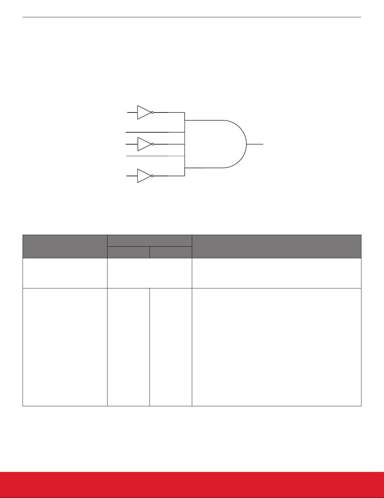
5.3.8 Output Enable/Disable
Clock outputs are disabled by four signals within Si5341/40 and the OEB pin:
OUTALL_DISABLE_LOW
•
• SYSINCAL
• OUTx_OE
• LOL
• OEB pin
The following figure shows the logic of how these disable/enables occur.
1 instance of this is used per output driver
LOL
OUTALL_DISABLE_LOW
OEB Pin
OUTX_OE
SYSINCAL
Si5341, Si5340 Rev D Family Reference Manual
Output Clocks
Enable to Individual
Output Drivers
OUTX_OE are the individual Output Driver enables as shown in the table below
Table 5.7. Output Enable/Disable Control Registers
Hex Address [Bit Field]
Setting Name
Si5341 Si5340
OUTALL_DISABLE_LOW 0102[0]
OUT0_OE
OUT1_OE
OUT2_OE
OUT3_OE
OUT4_OE
OUT5_OE
OUT6_OE
0108[1]
010D[1]
0112[1]
0117[1]
011C[1]
0121[1]
0126[1]
Figure 5.4. Output Enable
0 = Disables all outputs.
1 = All outputs are not disabled by this signal but may be disabled
by other signals or the OEB pin. See figure above.
0112[1]
0117[1]
0126[1]
012B[1]
0 = Specific output disabled.
—
1 = Specific output is not disabled. The OEB pin or other signals
—
within the device may be causing an output disable. See figure
above.
—
Function
OUT7_OE
OUT8_OE
OUT9_OE
silabs.com | Building a more connected world. Rev. 1.3 | 29
012B[1]
0130[1]
013A[1]
—
—
—
Page 30
Si5341, Si5340 Rev D Family Reference Manual
Output Clocks
5.3.9 Output Driver State When Disabled
disabled state of an output driver is configurable as: disable low, disable high, or disable mid. When set for disable mid, the output
The
common mode voltage will stay nearly the same when disabled as when enabled. The output common mode voltage is maintained
while the driver is disabled, reducing enable/disable transients. By contrast, powering down the driver rather than disabling it increases
output impedance and shuts off the output common mode voltage. For all output drivers connected in the system, it is recommended to
use Disable rather than Powerdown to reduce enable/disable common mode transients. Unused outputs may be left unconnected, powered down to reduce current draw, and, with the corresponding VDDOx, left unconnected.
Table 5.8. Output Driver Disable State Control Registers
Setting Name
Function
Si5341 Si5340
Hex Address [Bit Field]
OUT0_DIS_STATE
OUT1_DIS_STATE
OUT2_DIS_STATE
OUT3_DIS_STATE
0109[5:4]
010E[5:4]
0113[5:4]
0118[5:4]
0113[5:4]
0118[5:4]
0127[5:4]
012C[5:4]
Determines the state of an output driver when disabled. Selecta-
OUT4_DIS_STATE
OUT5_DIS_STATE
011D[5:4]
0122[5:4]
—
—
ble as:
Disable logic low.
•
• Disable logic high
OUT6_DIS_STATE
OUT7_DIS_STATE
OUT8_DIS_STATE
OUT9_DIS_STATE
0127[5:4]
012C[5:4]
0131[5:4]
013B[5:4]
—
—
—
—
5.3.10 Synchronous/Asynchronous Output Disable Feature
Outputs
can be configured to disable synchronously or asynchronously. In synchronous disable mode the output will wait until a clock
period has completed before the driver is disabled. This prevents unwanted runt pulses from occurring when disabling an output. In
asynchronous disable mode the output clock will disable immediately without waiting for the period to complete.
Setting Name
OUT0_SYNC_EN
OUT1_SYNC_EN
OUT2_SYNC_EN
OUT3_SYNC_EN
OUT4_SYNC_EN
OUT5_SYNC_EN
OUT6_SYNC_EN
OUT7_SYNC_EN
OUT8_SYNC_EN
OUT9_SYNC_EN
Table 5.9. Synchronous Disable Control Registers
Hex Address [Bit Field]
Si5341 Si5340
0109[3]
010E[3]
0113[3]
0118[3]
011D[3]
0113[3]
0118[3]
0127[3]
012C[3]
—
When this bit is high, the output will turn on/off (enable/disable)
without generating runt pulses or glitches. The default for this bit
is high. When this bit is low, the outputs will turn on/off asynchro-
0122[3]
0127[3]
012C[3]
0131[3]
013B[3]
—
—
—
—
—
nously. In this case, there may be glitches on the output when it
turns on/off.
Function
silabs.com | Building a more connected world. Rev. 1.3 | 30
Page 31

Si5341, Si5340 Rev D Family Reference Manual
Output Clocks
5.4 Output Crosspoint
output crosspoint allows any of the N dividers to connect to any of the R dividers and output drivers. Note that each output driver
The
has a specific R divider that is permanently attached and has the same subscript in the name, i.e., R3 and OUT3.
Table 5.10. Output Crosspoint Control Registers
Setting Name
OUT0_MUX_SEL
OUT1_MUX_SEL
OUT2_MUX_SEL
OUT3_MUX_SEL
OUT4_MUX_SEL
OUT5_MUX_SEL
OUT6_MUX_SEL
OUT7_MUX_SEL
OUT8_MUX_SEL
OUT9_MUX_SEL
Hex Address [Bit Field]
Si5341 Si5340
010B[2:0]
0110[2:0]
0115[2:0]
011A[2:0]
011F[2:0]
0124[2:0]
0129[2:0]
012E[2:0]
0133[2:0]
013D[2:0]
0115[2:0]
011A[2:0]
0129[2:0]
012E[2:0]
—
—
—
—
—
—
Function
Connects the output drivers to one of the N dividers. Selections
are N0, N1, N2, N3, and N4 for each output divider.
silabs.com | Building a more connected world. Rev. 1.3 | 31
Page 32

Si5341, Si5340 Rev D Family Reference Manual
Output Clocks
5.5 Zero Delay Mode
A zero delay mode is available for applications that require fixed and consistent minimum delay between the selected input and outputs.
The zero delay mode is configured by opening the internal feedback loop through software configuration and closing the loop externally.
helps to cancel out the internal delay introduced by the dividers, the crosspoint, the input, and the output drivers. Any one of the
This
outputs can be fed back to the FB_IN pins, although using the output driver that achieves the shortest trace length will help to minimize
the input-to-output delay. The OUT9 and FB_IN pins are recommended for the external feedback connection in the Si5341. OUT3 and
FB_IN pins are recommended for the external feedback in the Si5340. The FB_IN input pins must be terminated and ac-coupled when
zero delay mode is used. A differential external feedback path connection is necessary for best performance. For this reason, customers should avoid using CMOS outputs for driving the external feedback path. Zero Delay Mode performance will degrade with low values of phase detector frequency (Fpfd). For this reason, ClockBuilder Pro will not enable Zero Delay Mode with an Fpfd of less than
128 kHz.
When the DSPLL is set for Zero-Delay Mode (ZDM), a hard reset request from either the RSTb pin or RST_REG register bit will have a
delay of ~750 ms before executing. Any subsequent register writes to the device should be made after this time expires or they will be
overwritten with the NVM values. Please contact Silicon Labs technical support for information on reducing this ZDM hard reset time.
IN0
IN0
IN1
IN1
IN2
IN2
IN3/FB_IN
100
IN3/FB_IN
÷P
÷P
÷P
÷P
÷M
0
1
2
3
4
Si5341
15GHz
LPFPD
÷5
÷R
÷R
÷R
÷R
÷R
÷R
VDDO0
0
1
2
7
8
9
OUT0
OUT0
VDDO1
OUT1
OUT1
VDDO2
OUT2
OUT2
VDDO7
OUT7
OUT7
VDDO8
OUT8
OUT8
VDDO9
OUT9
OUT9
0
1
2
3
DSPLL
÷N
÷N
÷N
÷N
÷N
External Feedback Path
Si5341 Zero Delay Mode Setup
The following table gives the register used for the Zero Delay mode.
silabs.com | Building a more connected world. Rev. 1.3 | 32
Page 33

Table 5.11. Zero Delay Mode Register:
Reg Address Bit Field Type Setting Name Description
0x091C 2:0 R/W ZDM_EN 3 = Zero delay mode.
4 = Normal mode.
All other values must not be written.
Si5341, Si5340 Rev D Family Reference Manual
Output Clocks
silabs.com | Building a more connected world. Rev. 1.3 | 33
Page 34

Si5341, Si5340 Rev D Family Reference Manual
Digitally Controlled Oscillator (DCO) Modes
6. Digitally Controlled Oscillator (DCO) Modes
An output that is controlled as a DCO is useful for simple tasks such as frequency margining, CPU speed control, or just changing the
output frequency. The output can also be used for more sophisticated tasks such as FIFO management by adjusting the frequency of
the read or write clock to the FIFO or using the output as a variable Local Oscillator in a radio application.
6.1 Using the N Dividers for DCO Applications
The N dividers can be digitally controlled to so that all outputs connected to the N divider change frequency in real time without any
transition glitches. There are two ways to control the N divider to accomplish this task:
• Use the Frequency Increment/Decrement Pins or register bits.
• Write directly to the numerator or denominator of the N divider.
The output N divider can be changed from its minimum value of 10 to its maximum value of 4095 in very small fractional increments or
a single very large increment. Each N divider has a value of Nx_NUM/Nx_DEN. Nx_NUM is a 44 bit word and Nx_DEN is a 32 bit word.
Clockbuilder Pro left shifts these values as far as possible before writing them to the actual Nx_NUM and Nx_DEN registers. For example, an integer Nx divider of 30/1, when left shifted, becomes Nx_NUM = 64424509440 (decimal) and Nx_DEN = 2147483648 (decimal). By adjusting the size of the Nx_NUM and Nx_DEN but keeping the ratio the same, the resolution of the LSbit of numerator or
denominator can be controlled.
When changing the N divider(s) to fractional values, the setting name N_PIBYP[4:0] must be a 0 for the N divider that is being changed.
This applies when using FINC/FDEC or when directly writing to the N divider.
6.1.1 DCO with Frequency Increment/Decrement Pins/Bits
The FSTEPW (Frequency STEP Word) is a 44 bit word that is used to change the value of the Nx_NUM word. Whenever an FINC or
FDEC is asserted, the FSTEPW will automatically add or subtract from the Nx_NUM word so that the output frequency will increment
(FINC) or decrement (FDEC) respectively.
Each of the N dividers can be independently stepped up or down in numerical predefined steps with a maximum resolution that varies
from ~ 0.05 ppb to a ~0.004 ppb depending upon the frequency plan. One or more N dividers can be controlled by FINC/FDEC at the
same time by use of the N_FSTEP_MSK bits. Any N divider that is masked by its corresponding bit in the N_FSTEP_MSK field will not
change when FINC or FDEC is asserted. The magnitude of the frequency change caused by FINC or FDEC is determined by the value
of the FSTEPW word and the magnitude of the word in Nx_NUM. For a specific frequency step size it may be necessary to adjust the
Nx_NUM value while keeping the ratio of Nx_NUM/Nx_DEN the same. When the FINC or FDEC pin or register bit is asserted the selected N dividers will have their numerator changed by the addition or subtraction of the Nx_FSTEPW so that an FINC will increase the
output frequency and an FDEC will decrease the output frequency. An FINC or FDEC can be followed by another FINC or FDEC in 1
µs minimum.
Because the output frequency = F
* Nx_DEN/(Rx * Nx_NUM), subsequent changes to Nx_NUM by the FSTEPW will not produce
VCO
exactly the same output frequency change. The amount of error in the frequency step is extremely small and in a vast number of applications will not cause a problem. When consecutive frequency steps must be exactly the same, it is possible to set FINC and FDEC to
change the Nx_DEN instead of Nx_NUM and then consecutive FINCs or FDECs will be exactly the same frequency change. However,
there are some special setups that are necessary to achieve this. For more information contact Silicon Labs.
6.1.2 DCO with Direct Register Writes
When a N divider numerator (Nx_NUM) and its corresponding update bit (Nx_UPDATE) is written, the new numerator value will take
effect and the output frequency will change without any glitches. The N divider numerator and denominator terms (Nx_NUM and
Nx_DEN) can be left and right shifted so that the least significant bit of the numerator word represents the exact step resolution that is
needed for your application. Each N divider has an update bit (Nx_UPDATE) that must be written to cause the written values to take
effect. All N dividers can be updated at the same time by writing the N_UPDATE_ALL bit. Note that writing this bit will not cause any
output glitching on an N divider that did not have its numerator or denominator changed.
When changing the N divider denominator (Nx_DEN) it is remotely possible that a small phase change of ~550 fs may occur at the
exact time of the frequency change. However with the proper setup it is possible to change Nx_DEN and never have a phase change. If
your application requires changing an N divider denominator, contact Silicon Labs.
6.2 Using the M Divider for DCO Applications
The VCO can be treated as a DCO by changing the value of the M feedback divider. By changing the M divider, all the output frequencies will change by the same amount in ppm. Changing the M divider is only valid for small changes in the output frequencies. Contact
Silicon Labs for assistance in the implementation of this capability.
silabs.com | Building a more connected world. Rev. 1.3 | 34
Page 35

Si5341, Si5340 Rev D Family Reference Manual
Dynamic PLL Changes
7. Dynamic PLL Changes
7.1 Revisions B and A
It is possible for a PLL to become unresponsive (i.e., lose lock indefinitely) when it is dynamically reprogrammed or changed via the
serial port. Reprogramming/changing the N divider does not affect the PLL. Any change that causes the VCO frequency to change by
more than 250 ppm since Power-up, NVM download, or SOFT_RST requires the following special sequence of writes. Changes to the
following registers require the following special sequence of writes:
• XAXB_FREQ_OFFSET
• PXAXB
• MXAXB_NUM
• MXAXB_DEN
• M_NUM
• M_DEN
1. First, the preamble:
Write 0x0B24 = 0xD8
Write 0x0B25 = 0x00
Write 0x0502 = 0x01
Write 0x0505 = 0x03
Write 0x0957 = 0x17
Write 0x0B4E = 0x1A
2. Wait 300 ms.
3. Then, perform the desired register modifications.
4. Write SOFT_RST - 0x001C[0] = 1
5. Write the post-amble:
Write 0x0B24 = 0xDB
Write 0x0B25 = 0x02
7.2 Revision D
The Revision D preamble and postamble values for updating certain registers during device operation have changed after Revision B.
Either the new or old values below may be written to Revision D or later devices without issue. No system software changes are necessary for legacy systems. When writing old values, note that reading back these registers will not give the written old values, but will
reflect the new values. Silicon Labs recommends using the new values for all Revision D and later designs, since the write and read
values will match.
The device revision can be determined in the setting DEVICE_REV, register 0x0005.
DEVICE_REV = 0x02 or higher: New Values
Revision D Preamble: 0x0B24 = 0xC0, 0x0B25 = 0x00
Revision D Postamble: 0x0B24 = 0xC3, 0x0B25 = 0x02
Note that revision B and earlier devices must continue to use the original values for these registers:
DEVICE_REV = 0x00 or 0x01: Old Values
Revision B Preamble: 0x0B24 = 0xD8, 0x0B25 = 0x00
Revision B Postamble: 0x0B24 = 0xDB, 0x0B25 = 0x02
silabs.com | Building a more connected world. Rev. 1.3 | 35
Page 36

Si5341, Si5340 Rev D Family Reference Manual
Dynamic PLL Changes
7.3 Dynamic Changes to Output Frequencies without Changing PLL Settings
This section applies to the following scenario:
CBPro generated register map "was" used to program either the volatile or the non-volatile memory of a Si5340/1. Changes to
1. A
output frequencies without changing the PLL settings are desired.
2. The CBPro project file can be used to look for the VCO frequency (FVCO), Ry, Nx values for each OUTy in the design report
and/or the datasheet addendum.
OUTy = FVCO/(Nx * Ry)
Solve for Nx based on the desired OUTy. The Nx dividers can be digitally controlled to so that all outputs connected to the Nx divider
change frequency in real time without any transition glitches. There are two ways to control the Nx divider to accomplish this task:
1. Use the Frequency Increment/Decrement Pins or register bits.
2. Write directly to the numerator or denominator of the Nx divider.
The details of both methods are covered in 6.1 Using the N Dividers for DCO Applications.
7.4 Dynamic Changes to Output Frequencies while Changing PLL Settings Using a CBPro Register Map
This section applies to the following scenario:
1. A CBPro generated register map "is" used to program either the voltatile or the non-volatile memory of a Si5340/1.
2. This needs a register write sequence provided in the CBPro export section as shown below.
Figure 7.1. CBPro Register Write Sequence While Changing PLL Settings
silabs.com | Building a more connected world. Rev. 1.3 | 36
Page 37

Si5341, Si5340 Rev D Family Reference Manual
Serial Interface
8. Serial Interface
Configuration and operation of the Si5341/40 is controlled by reading and writing registers using the I2C or SPI interface. Both of these
serial interfaces are based upon 8-bit addressing, which means that the page byte must be written every time you need to access a
different page in the register map. See the PGE byte at register 0x0001 for more information. The I2C_SEL pin selects I2C or SPI operation. The Si5341/40 supports communication with a 3.3 V or 1.8 V host by setting the IO_VDD_SEL (0x0943[0]) configuration bit. The
SPI mode supports 4-wire or 3-wire by setting the SPI_3WIRE configuration bit.
Host = 1.8V
Host = 3.3V
I2C_SEL pin = High
IO_VDD_SEL = VDD
1.8V
2
I
C
SDA
HOST
SCLK
IO_VDD_SEL = VDDA
3.3V
2
I
C
SDA
HOST
SCLK
2
I
C
SPI 4-Wire SPI 3-Wire
I2C_SEL pin = Low
SPI_3WIRE = 0
IO_VDD_SEL = VDD
(Default) (Default)
1.8V
VDDA
1.8V3.3V
VDD
Si5341/40
SPI
HOST
CS
SDO
SDI
SCLK
CS
SDO
SCLK
1.8V
SDA
SCLK
IO_VDD_SEL = VDDA IO_VDD_SEL = VDDA
3.3V
VDDA
1.8V3.3V
VDD
Si5341/40
SPI
HOST
CS
SDO
SDI
SCLK
CS
SDO
SCLK
3.3V
SDA
SCLK
I2C_SEL pin = Low
SPI_3WIRE
IO_VDD_SEL = VDD
(Default)
1.8V3.3V
VDD
VDDA
SDI
Si5341/40 Si5341/40
1.8V3.3V
VDD
VDDA
SDI
Si5341/40
SPI
HOST
SPI
HOST
1.8V
3.3V
CS
SDIO
SCLK
CS
SDIO
SCLK
VDDA
CS
SDIO
SCLK
VDDA
CS
SDIO
SCLK
= 1
1.8V3.3V
VDD
1.8V3.3V
VDD
Si5341/40
Figure 8.1. I2C/SPI Device Connectivity Configurations
The following table lists register settings of interest for the I2C/SPI.
Table 8.1. I2C/SPI Register Settings
Hex Address [Bit Field]
Register Name
Si5341 Si5340
IO_VDD_SEL 0x0943[0] 0x0943[0]
SPI_3WIRE 0x002B[3] 0x002B[3]
Function
The IO_VDD_SEL configuration bit optimizes the VIL, VIH, VOL,
and VOH thresholds to match the VDDS voltage. By default the
IO_VDD_SEL bit is set to the VDD option. The serial interface
pins are always 3.3 V tolerant even when the device's VDD pin is
supplied from a 1.8 V source. When the I2C or SPI host is operat-
ing at 3.3 V and the Si5340/41 at VDD = 1.8 V, the host must
write the IO_VDD_SEL configuration bit to the VDDA option. This
will ensure that both the host and the serial interface are operating
at the optimum voltage thresholds.
The SPI_3WIRE configuration bit selects the option of 4-wire or 3wire SPI communication. By default the SPI_3WIRE configuration
bit is set to the 4-wire option. In this mode the Si5341/40 will accept write commands from a 4-wire or 3- wire SPI host allowing
configuration of device registers. For full bidirectional communication in 3-wire mode, the host must write the SPI_3WIRE configuration bit to “1”.
If neither serial interface is used, leave pins I2C_SEL, A1/SDO and A0/CS disconnected and tie SDA/SDIO and SCLK low.
silabs.com | Building a more connected world. Rev. 1.3 | 37
Page 38

Si5341, Si5340 Rev D Family Reference Manual
Serial Interface
8.1 I2C Interface
When
in I2C mode, the serial interface operates in slave mode with 7-bit addressing and can operate in Standard-Mode (100 kbps) or
Fast-Mode (400 kbps) and supports burst data transfer with auto address increments. The I2C bus consists of a bidirectional serial data
line (SDA) and a serial clock input (SCL) as shown in Figure 8.12 SPI “Burst Data Write” Instruction Timing on page 43. Both the SDA
and SCL pins must be connected to a supply via an external pull-up (1k to 4.7k ohm) as recommended by the I2C specification as
shown in the figure below. Two address select bits (A0, A1) are provided allowing up to four Si5341/40 devices to communicate on the
same bus. This also allows four choices in the I2C address for systems that may have other overlapping addresses for other I2C devices.
VDDI2C
VDD
I2C
I2C_SEL
SDA
To I2C Bus or
H
ost
SCLK
A0
LSBs of I2C
ress
Add
Figure 8.2. I2C Configuration
The 7-bit slave device address of the Si5341/40 consists of a 5-bit fixed address plus two pins that are selectable for the last two bits,
as shown in the following figure.
Slave Address
Figure 8.3. 7-bit I2C Slave Address Bit-Configuration
1 1 1 0 1 A0
A1
Si5341/40
0123456
A1
Data is transferred MSB first in 8-bit words as specified by the I2C
address + a write bit, an 8-bit register address, and 8 bits of data as shown in Figure 8.4 I2C Write Operation on page 39. A write
burst operation is also shown where subsequent data words are written using to an auto-incremented address.
silabs.com | Building a more connected world. Rev. 1.3 | 38
specification. A write command consists of a 7-bit device (slave)
Page 39

Si5341, Si5340 Rev D Family Reference Manual
Write Operation – Single Byte
S 0 A Reg Addr [7:0]Slv Addr [6:0] A Data [7:0] PA
Write Operation - Burst (Auto Address Increment)
S 0 A Reg Addr [7:0]Slv Addr [6:0] A Data [7:0] A Data [7:0] PA
Reg Addr +1
Serial Interface
Host
Host
Si5341/40
Si5341/40
1 – Read
0 – Write
A – Acknowledge (SDA LOW)
N – Not Acknowledge (SDA HIGH)
S – START condition
P – STOP condition
Figure 8.4. I2C Write Operation
A read operation is performed in two stages. A data write is used to set the register address, then a data read is performed to retrieve
the data from the set address. A read burst operation is also supported as shown in the following figure.
Read Operation – Single Byte
S 0 A Reg Addr [7:0]Slv Addr [6:0] A P
S 1 ASlv Addr [6:0] Data [7:0] PN
Read Operation - Burst (Auto Address Increment)
S 0 A Reg Addr [7:0]Slv Addr [6:0] A P
S 1 ASlv Addr [6:0] Data [7:0] A PNData [7:0]
Reg Addr +1
Host
Si5341/40
1 – Read
0 – Write
Host
Si5341/40
A – Acknowledge (SDA LOW)
N – Not Acknowledge (SDA HIGH)
S – START condition
P – STOP condition
Figure 8.5. I2C Read Operation
silabs.com | Building a more connected world. Rev. 1.3 | 39
Page 40

Si5341, Si5340 Rev D Family Reference Manual
Serial Interface
8.2 SPI Interface
in SPI mode, the serial interface operates in 4-wire or 3-wire depending on the state of the SPI_3WIRE configuration bit. The 4-
When
wire interface consists of a clock input (SCLK), a chip select input (CS), serial data input (SDI), and serial data output (SDO). The 3wire interface combines the SDI and SDO signals into a single bidirectional data pin (SDIO). Both 4-wire and 3-wire interface connections are shown in the following figure.
SPI 3-Wire
SPI_3WIRE = 1
I2C_SEL
SPI 4-Wire
SPI_3WIRE = 0
I2C_SEL
CS
CS
SDI
To SPI Host
SDO
To SPI Host
To SPI Host
SDIO
SCLK
SCLK
Si5340/41
Figure 8.6. SPI Interface Connections
Table 8.2. SPI Command Format
Instruction
Set Address 000x xxxx 8-bit Address — —
Write Data 010x xxxx 8-bit Data — —
Ist Byte
11
2nd Byte 3rd Byte nth Byte
Si5340/41
2, 3
Read Data 100x xxxx 8-bit Data — —
Write Data + Address Increment 011x xxxx 8-bit Data — —
Read Data + Address Increment 101x xxxx 8-bit Data — —
Burst Write Data 1110 0000 8-bit Address 8-bit Data 8-bit Data
1. X = don’t care (1 or 0)
2.
The Burst Write Command is terminated by de-asserting CSb (CSb = high)
3. There is no limit to the number of data bytes that may follow the Burst Write command, but the address will wrap around to 0 in
the byte after address 255 is written.
Writing or reading data consist of sending a “Set Address” command followed by a “Write Data” or “Read Data” command. The 'Write
+ Address Increment' or “Read Data + Address Increment” commands are available for cases where multiple byte operations in
Data
sequential address locations is necessary. The “Burst Write Data” instruction provides a compact command format for writing data
since it uses a single instruction to define starting address and subsequent data bytes. The following figure shows an example of writing
three bytes of data using the write commands. This demonstrates that the “Write Burst Data” command is the most efficient method for
writing data to sequential address locations.
silabs.com | Building a more connected world. Rev. 1.3 | 40
Page 41

Si5341, Si5340 Rev D Family Reference Manual
‘Set Address’ and ‘Write Data’
‘Set Addr’ Addr [7:0] ‘Write Data’ Data [7:0]
‘Set Addr’ Addr [7:0] ‘Write Data’ Data [7:0]
‘Set Addr’ Addr [7:0] ‘Write Data’ Data [7:0]
‘Set Address’ and ‘Write Data + Address Increment’
‘Set Addr’ Addr [7:0] ‘Write Data + Addr Inc’ Data [7:0]
‘Write Data + Addr Inc’ Data [7:0]
‘Write Data + Addr Inc’ Data [7:0]
‘Burst Write Data’
‘Burst Write Data’ Addr [7:0] Data [7:0] Data [7:0] Data [7:0]
Serial Interface
Si5341/40Host
Si5341/0Host
Figure 8.7. Example Writing Three Data Bytes Using the Write Commands
The following figure provides a similar comparison for reading data with the read commands. Note that there is no burst read, only read
increment.
‘Set Address’ and ‘Read Data’
‘Set Addr’ Addr [7:0] ‘Read Data’ Data [7:0]
‘Set Addr’ Addr [7:0] ‘Read Data’ Data [7:0]
‘Set Addr’ Addr [7:0] ‘Read Data’ Data [7:0]
‘Set Address’ and ‘Read Data + Address Increment’
‘Set Addr’ Addr [7:0] ‘Read Data + Addr Inc’ Data [7:0]
‘Read Data + Addr Inc’ Data [7:0]
‘Read Data + Addr Inc’ Data [7:0]
Si5341/40Host
Si5341/40Host
Figure 8.8. Example of Reading Three Data Bytes Using the Read Commands
The timing diagrams for the SPI commands are shown in the following figures.
silabs.com | Building a more connected world. Rev. 1.3 | 41
Page 42

Si5341, Si5340 Rev D Family Reference Manual
Serial Interface
Previous
Command
CS
SCLK
4-Wire
SDI
SDO
3-Wire
SDIO
‘Set Address’ Command
> 2 SCLK
Periods
Set Address Instruction Base Address
1
0
1
0
Si5341/40Host
01234567
7
01234567
7
Si5341/40Host
Don’t Care
0123456
0123456
High Impedance
> 2.0
SCLK
Periods
Next Command
7
6
7
6
Figure 8.9. SPI “Set Address” Command Timing
Previous
Command
CS
> 2
SCLK
Periods
‘Write Data’ or ‘Write Data + Address Increment’
Command
Write Data instruction
Data byte @ base address + 1
> 2.0
SCLK
Periods
SCLK
4-Wire
SDI
1
0
01234567
01234567
7
SDO
3-Wire
SDIO
1
0
Si5341/40Host
01234567
Si5341/40Host
Don’t Care
01234567
High Impedance
7
Figure 8.10. SPI “Write Data” and “Write Data+ Address Increment” Instruction Timing
Next
Command
6
6
silabs.com | Building a more connected world. Rev. 1.3 | 42
Page 43

Si5341, Si5340 Rev D Family Reference Manual
Serial Interface
Previous
Command
> 2.0
SCLK
Periods
‘Read Data’ or ‘Read Data + Address Increment’
Command
Read Data instruction
Read byte @ base address + 1
> 2.0
SCLK
Periods
Next
Command
CS
SCLK
4-Wire
SDI
SDO
1
0
1
0
01234567
01234567
7
6
7
6
3-Wire
SDIO
1
0
Si5341/40Host
01234567
Si5341/40Host
Don’t Care
01234567
High Impedance
7
6
Figure 8.11. SPI “Read Data” and “Read Data + Address Increment” Instruction Timing
Previous
Command
CS
‘Burst Data Write’ Command
> 2.0
SCLK
Periods
Burst Write Instruction Base address
st
1
data byte @ base address
th
n
data byte @ base address +n
> 2.0
SCLK
Periods
Next
Command
SCLK
4-Wire
SDI
1
0
01234567
7
0123456 0123456 01234567
7
7
6
SDO
3-Wire
SDIO
1
0
Si5341/40Host
01234567
7 7 7
Si5341/40Host
Don’t Care
0123456 0123456 0123456
High Impedance
7
6
Note that for all SPI communication the chip select (CS) must be high for the minimum time period between commands. When chip
select goes high it indicates the termination of the command. The SCLK can be turned off between commands, particularly if there are
very long delays between commands.
Figure 8.12. SPI “Burst Data Write” Instruction Timing
silabs.com | Building a more connected world. Rev. 1.3 | 43
Page 44

Si5341, Si5340 Rev D Family Reference Manual
Field Programming
9. Field Programming
To simplify design and software development of systems using the Si5341/40, a field programmer is available. The ClockBuilder Pro
Field Programmer supports both “in-system” programming (for devices already mounted on a PCB) as well as “in-socket” programming
of Si5341/40 sample devices. Refer to the https://www.silabs.com/products/development-tools/timing/cbprogrammer product web page
for information about this kit.
silabs.com | Building a more connected world. Rev. 1.3 | 44
Page 45

Si5341, Si5340 Rev D Family Reference Manual
Recommended Crystals and External Oscillators
10. Recommended Crystals and External Oscillators
Please refer to the Si534x/8x Jitter Attenuators Recommended Crystal, TCXO and OCXOs Reference Manual for more information.
silabs.com | Building a more connected world. Rev. 1.3 | 45
Page 46

Si5341, Si5340 Rev D Family Reference Manual
Crystal and Device Circuit Layout Recommendations
11. Crystal and Device Circuit Layout Recommendations
The main layout issues that should be carefully considered include the following:
•
Number and size of the ground vias for the Epad (see Section 12.3 Grounding Vias for details)
• Output clock trace routing
• Input clock trace routing
• Control and Status signals to input or output clock trace coupling
• XTAL signal coupling
• XTAL layout
If the application uses a crystal for the XAXB inputs a shield should be placed underneath the crystal connected to the X1 and X2 pins
(4 and 7) to provide the best possible performance. The shield should not be connected to the ground plane and the planes underneath
should have as little under the shield as possible. It may be difficult to do this for all the layers, but it is important to do this for the layers
that are closest to the shield.
Refer to the High Performance Clock Generator Kits on the Clock Development Tools web page for the Si5341-EVB and Si5340-EVB
schematics, layout, and BOM files.
11.1 64-Pin QFN Si5341 Layout Recommendations
This section details the recommended guidelines for the crystal layout of the 64-pin Si5341 device using an example 8-layer PCB. Following are descriptions of each of the eight layers.
• Layer 1: device layer, with low speed CMOS control/status signals, ground flooded
• Layer 2: crystal shield
• Layer 3: ground plane
• Layer 4: power distribution
• Layer 5: power routing layer
• Layer 6: input clocks
• Layer 7: output clocks layer
• Layer 8: ground layer
Figure 11.1 64-pin Si5341 Crystal Layout Recommendations Top Layer (Layer 1) on page 47 is the top layer layout of the Si5341
device mounted on the top PCB layer. This particular layout was designed to implement either a crystal or an external oscillator as the
XAXB reference. The crystal/ oscillator area is outlined with the white box around it. In this case, the top layer is flooded with ground.
Note that this layout has a resistor in series with each pin of the crystal. In typical applications, these resistors should be removed.
11.1.1 Si5341 Applications without a Crystal
If the application does not use a crystal, then the X1 and X2 pins should be left as “no connect” and should not be tied to ground. In
addition, there is no need for a crystal shield or the voids underneath the shield. If there is a differential external clock input on XAXB
there should be a termination circuit near the XA and XB pins. This termination circuit should be two 50 Ω resistors and one 0.1 μF cap
connected in the same manner as on the other clock inputs (IN0, IN1 and IN2). See Figure 4.1 Crystal Resonator and External Refer-
ence Clock Connection Options on page 16. The clock input on XAXB must be ac-coupled. Care should be taken to keep all clock
inputs well isolated from each other as well as any other dynamic signal. For LVCMOS or clipped sine wave inputs on XAXB, see
Figure 4.1 Crystal Resonator and External Reference Clock Connection Options on page 16.
silabs.com | Building a more connected world. Rev. 1.3 | 46
Page 47

Si5341, Si5340 Rev D Family Reference Manual
Crystal and Device Circuit Layout Recommendations
11.1.2 Si5341 Crystal Layout Guidelines
The following are five recommended crystal layout guidelines:
Place the crystal as close as possible to the XA/XB pins.
1.
2. Do not connect the crystal's GND pins to PCB gnd.
3. Connect the crystal's GND pins to the DUT's X1 and X2 pins via a local crystal shield placed around and under the crystal. Make
sure that X1, X2, and both crystal ground pins do NOT connect to the pcb ground. See Figure 11.1 64-pin Si5341 Crystal Layout
Recommendations Top Layer (Layer 1) on page 47 for an illustration of how to create a crystal shield by placing vias connecting
the top layer traces to the shield layer underneath. Note that a zoom view of the crystal shield layer on the next layer down is
shown in Figure 11.2 Zoom View Crystal Shield Layer, Below the Top Layer (Layer 2) on page 48.
4. Keep transitioning signal traces as distant as practical from the crystal/oscillator area especially if they are clocks or frequently toggling digital signals.
5. In general, do not route GND, power planes/traces, or locate components on the other side below the crystal shield. If necessary, a
ground layer may be placed under the crystal shield plane as long as it is at least 0.05” below the crystal shield layer.
Figure 11.1. 64-pin Si5341 Crystal Layout Recommendations Top Layer (Layer 1)
Note the vias that are shown for the center ground pad so that there is a low-impedance path to ground and a good thermal path to
ground. See 12.3 Grounding Vias for details on these vias.
following figure shows the layer that implements the shield underneath the crystal. The shield extends underneath the entire crystal
The
and the X1 and X2 pins. This layer also has the clock input pins. The clock input pins go to Layer 2 using vias to avoid crosstalk. As
soon as the clock inputs are on Layer 2, they have a ground shield above below and on the sides for protection.
silabs.com | Building a more connected world. Rev. 1.3 | 47
Page 48

Si5341, Si5340 Rev D Family Reference Manual
Crystal and Device Circuit Layout Recommendations
Figure 11.2. Zoom View Crystal Shield Layer, Below the Top Layer (Layer 2)
The following figure of the ground plane shows a void underneath the crystal shield.
Figure 11.3. Crystal Ground Plane (Layer 3)
The figure below is a power plane and shows the clock output power supply traces. The void underneath the crystal shield is continued.
silabs.com | Building a more connected world. Rev. 1.3 | 48
Page 49

Si5341, Si5340 Rev D Family Reference Manual
Crystal and Device Circuit Layout Recommendations
Figure 11.4. Power Plane (Layer 4)
The following figure shows Layer 5, which is the power plane with the power routed to the clock output power pins.
Figure 11.5. Layer 5 Power Routing on Power Plane (Layer 5)
The following figure is another ground plane similar to Layer 3.
silabs.com | Building a more connected world. Rev. 1.3 | 49
Page 50

Si5341, Si5340 Rev D Family Reference Manual
Crystal and Device Circuit Layout Recommendations
Figure 11.6. Ground Plane (Layer 6)
silabs.com | Building a more connected world. Rev. 1.3 | 50
Page 51

11.1.3 Output Clocks
Si5341, Si5340 Rev D Family Reference Manual
Crystal and Device Circuit Layout Recommendations
Similar
to the input clocks, the output clocks have vias that immediately go to a buried layer with a ground plane above them and a
ground flooded bottom layer. There is a ground flooding between the clock output pairs to avoid crosstalk. The figure below shows the
output clocks.
Figure 11.7. Output Clock Layer (Layer 7)
As shown in the figure below, there should be a line of vias through the ground flood on either side of the output clocks to ensure that
the ground flood immediately next to the differential pairs has a low inductance path to the ground plane on Layers 3 and 6.
Figure 11.8. Bottom Layer Ground Flooded (Layer 8)
silabs.com | Building a more connected world. Rev. 1.3 | 51
Page 52

Si5341, Si5340 Rev D Family Reference Manual
Crystal and Device Circuit Layout Recommendations
11.2 44-Pin QFN Si5340 Layout Recommendations
This section details the layout recommendations for the 44-pin Si5340 device using an example 6-layer PCB.
The following guidelines detail images of a six-layer board with the following stack:
Layer 1: device layer, with low speed CMOS control/status signals, ground flooded
•
• Layer 2: crystal shield, output clocks, ground flooded
• Layer 3: ground plane
• Layer 4: power distribution, ground flooded
• Layer 5: input clocks, ground flooded
• Layer 6: low-speed CMOS control/status signals, ground flooded
This layout was designed to implement either a crystal or an external clock as the XAXB reference. The top layer is flooded with
ground. The clock output pins go to Layer 2 using vias to avoid crosstalk during transit. When the clock output signals are on Layer 2
there is a ground shield above, below and on all sides for protection. Output clocks should always be routed on an internal layer with
ground reference planes directly above and below. The plane that has the routing for the output clocks should have ground flooded
near the clock traces to further isolate the clocks from noise and other signals.
11.2.1 Si5340 Applications without a Crystal as the Reference Clock
If the application does not use a crystal, then the X1 and X2 pins should be left as “no connect” and should not be tied to ground. In
addition, there is no need for a crystal shield or the voids underneath the shield. If there is a differential external clock input on XAXB
there should be a termination circuit near the XA and XB pins. This termination circuit should be two 50 Ω resistors and one 0.1 μF cap
connected in the same manner as on the other clock inputs (IN0, IN1 and IN2). The clock input on XAXB must be ac-coupled. Care
should be taken to keep all clock inputs well isolated from each other as well as from any other dynamic signal.
Figure 11.9. Device Layer (Layer 1)
Note the vias to ground from the center ground pad. These are needed to create a low-impedance path to ground and a good thermal
path to ground. See 12.3 Grounding Vias for additional information on these vias.
silabs.com | Building a more connected world. Rev. 1.3 | 52
Page 53

Si5341, Si5340 Rev D Family Reference Manual
Crystal and Device Circuit Layout Recommendations
11.2.2 Si5340 Crystal Guidelines
figure below is the second layer, which implements the shield underneath the crystal. The shield extends underneath the entire
The
crystal and the X1 and X2 pins. There should be no less than 12 vias to connect the X1X2 planes on Layers 1 and 2. These vias are
not shown in any other figures. All traces with signals that are not static must be kept well away from the crystal and the X1X2 plane.
Figure 11.10. Crystal Shield Layer 2
The following figure is the ground plane and shows a void underneath the crystal shield.
Figure 11.11. Ground Plane (Layer 3)
The following figure is a power plane showing the clock output power supply traces. The void underneath the crystal shield is continued.
silabs.com | Building a more connected world. Rev. 1.3 | 53
Page 54

Si5341, Si5340 Rev D Family Reference Manual
Crystal and Device Circuit Layout Recommendations
Figure 11.12. Power Plane and Clock Output Power Supply Traces (Layer 4)
following figure shows layer 5 and the clock input traces. Similar to the clock output traces, they are routed to an inner layer and
The
surrounded by ground to avoid crosstalk.
Figure 11.13. Clock Input Traces (Layer 5)
The following figure shows the bottom layer, which continues the void underneath the shield. Layer 6 and layer 1 are mainly used for
low
speed CMOS control and status signals for which crosstalk is not a significant issue. PCB ground can be placed under the X1X2
shield as long as the PCB ground is at least 0.05 inches below it.
silabs.com | Building a more connected world. Rev. 1.3 | 54
Page 55

Si5341, Si5340 Rev D Family Reference Manual
Crystal and Device Circuit Layout Recommendations
Figure 11.14. Low-Speed CMOS Control and Status Signal Layer 6 (Bottom Layer)
For
any high-speed, low-jitter application, the clock signal runs should be impedance-controlled to 100 Ω differential or 50 Ω singleended. Differential signaling is preferred because of its increased immunity to common-mode noise. All clock I/O runs should be properly terminated.
silabs.com | Building a more connected world. Rev. 1.3 | 55
Page 56

Si5341, Si5340 Rev D Family Reference Manual
Power Management
12. Power Management
12.1 Power Management Features
Several unused functions can be powered down to minimize power consumption. The registers listed in in the following table are used
for powering down different features.
Table 12.1. Power Management Registers
Register Name
PDN 0x001E[0]
OUT0_PDN
OUT1_PDN
OUT2_PDN
OUT3_PDN
OUT4_PDN
OUT5_PDN
OUT6_PDN
OUT7_PDN
OUT8_PDN
OUT9_PDN
OUT_PDN_ALL 0x0145[0] Power down all output drivers
XAXB_PDNB 0x090E[1]
Hex Address [Bit Field] Function
Si5341 Si5340
This bit allows powering down the device. The serial interface remains powered during power down mode.
0x0108[0]
0x010D[0]
0x0112[0]
0x0117[0]
0x011C[0]
0x0121[0]
0x0126[0]
0x012B[0]
0x0130[0]
0x013A[0]
0x0112[0]
0x011C[0]
0x0126[0]
0x012B[0]
—
Powers down unused clock outputs.
—
—
—
—
—
0-Power down the oscillator and buffer circuitry at the
XA/XB pins
1- No power down
12.2 Power Supply Recommendations
The
power supply filtering generally is important for optimal timing performance. The Si5341/0 devices have multiple stages of on-chip
regulation to minimize the impact of board level noise on clock jitter.
It is recommended to use a 0402, 1.0 μF ceramic capacitor on each VDD for optimal performance. Because of the extensive internal
voltage regulation this will be sufficient unless the power supply has very high noise. If the power supply might have very high noise,
then it is suggested to include an optional, single 0603 (resistor/ferrite) bead in series with each supply to enable additional filtering.
This resistor/ferrite should initially be a 0 Ω resistor. If additional supply filtering is needed then a ferrite component can replace the 0 Ω
resistor.
12.3 Grounding Vias
The pad on the bottom of the device functions as both the sole electrical ground and primary heat transfer path. Hence it is important to
minimize the inductance and maximize the heat transfer from this pad to the internal ground plane of the pcb. Use no less than 25 vias
from the center pad to a ground plane under the device. In general more vias will perform better. Having the ground plane near the top
layer will also help to minimize the via inductance from the device to ground and maximize the heat transfer away from the device.
silabs.com | Building a more connected world. Rev. 1.3 | 56
Page 57

Si5341, Si5340 Rev D Family Reference Manual
Power Management
12.4 Power Supply Sequencing
Four classes of supply voltages exist:
VDD = 1.8 V (Core digital supply)
1.
2. VDDA = 3.3 V (Analog supply)
3. VDDOx = 1.8/2.5/3.3 V ± 5% (Clock output supply)
4. VDDS = 1.8/3.3V ± 5% (Digital I/O supply)
A 1.0 µF cap is recommended for voltage bypass.
There is no requirement for power supply sequencing unless the output clocks are required to be phase aligned with each other. In this
case, the VDDO of each clock which needs to be aligned must be powered up before VDD and VDDA. VDDS has no effect on output
clock alignment.
If output-to-output alignment is required for applications where it is not possible to properly sequence the power supplies, then the output clocks can be aligned by asserting the SOFT_RST 0x001C[0] or Hard Reset 0x001E[1] register bits or driving the RSTB pin. Note
that using a hard reset will reload the register with the contents of the NVM and any unsaved changes will be lost.
One may observe that when powering up the VDD = 1.8 V rail first, that the VDDA = 3.3 V rail will initially follow the 1.8 V rail. Likewise,
if the VDDA rail is powered down first then it will not drop far below VDD until VDD itself is powered down. This is due to the pad I/O
circuits which have large MOSFET switches to select the local supply from either the VDD or VDDA rails. These devices are relatively
large and yield a parasitic diode between VDD and VDDA. Please allow for both VDD and VDDA to power-up and power-down before
measuring their respective voltages.
The internal POR (power on reset) will not happen until both VDD and VDDA have been applied.
silabs.com | Building a more connected world. Rev. 1.3 | 57
Page 58

Si5341, Si5340 Rev D Family Reference Manual
Base vs. Factory Preprogrammed Devices
13. Base vs. Factory Preprogrammed Devices
The Si5341/40 devices can be ordered as “base” or “factory-preprogrammed” (also known as “custom OPN”) versions.
13.1 “Base” Devices (Also Known as “Blank” Devices)
• Example “base” orderable part numbers (OPNs) are of the form “Si5341A-A-GM” or “Si5340B-A-GM”.
• Base devices are available for applications where volatile reads and writes are used to program and configure the device for a particular application.
• Base devices do not power up in a usable state (all output clocks are disabled).
• Base devices are, however, configured by default to use a 48 MHz crystal on the XAXB reference and a 1.8V compatible I/O voltage
setting for the host I2C/SPI interface.
• Additional programming of a base device is mandatory to achieve a usable configuration.
• See the on-line lookup utility to access the default configuration plan and register settings for any base OPN.
13.2 Factory Preprogrammed (Custom OPN) Devices
• Factory preprogammed devices use a “custom OPN”, such as Si5341A-A-xxxxx-GM, where xxxxx is a sequence of characters assigned by Silicon Labs for each customer-specific configuration. These characters are referred to as the “OPN ID”. Customers must
initiate custom OPN creation using the ClockBuilder Pro software.
• Many customers prefer to order devices which are factory preprogrammed for a particular application that includes specifying the
XAXB reference frequency/type, the clock input frequencies, the clock output frequencies, as well as the other options, such as automatic clock selection, loop BW, etc. The ClockBuilder software is required to select among all of these options and to produce a
project file which Silicon Labs uses to preprogram all devices with custom orderable part number (“custom OPN”).
• Custom OPN devices contain all of the initiialization information in their non-volatile memory (NVM) so that it powers up fully configured and ready to go.
• Because preprogrammed device applications are inherently quite different from one another, the default power up values of the register settings can be determined using the custom OPN utility.
• Custom OPN devices include a device top mark which includes the unique OPN ID. Refer to the device datasheet’s Ordering Guide
and Top Mark sections for more details.
Both “base” and “factory preprogrammed” devices can have their operating configurations changed at any time using volatile reads and
writes to the registers. Both types of devices can also have their current register configuration written to the NVM by executing an NVM
bank burn sequence (see 3.2 NVM Programming).
silabs.com | Building a more connected world. Rev. 1.3 | 58
Page 59

Si5341, Si5340 Rev D Family Reference Manual
Register Map
14. Register Map
14.1 Register Map Overview and Default Settings Values
The Si5341/40 family has a large register map and is divided into separate pages. Each page contains a total of 256 registers, although
all 256 registers are not used. Register 1 on each page is reserved to indicate the page and register 255 is reserved for the device
ready status. The following is a summary of the content that can be found on each of the pages. Note any page that is not listed is not
used for the device. Do not attempt to write to registers that have not been described in this document, even if they are accessible.
Note that the default value will depend on the values loaded into NVM, which is determined by the part number.
Where not provided in the register map information below, you can get the default values of the register map settings, by accessing the
part number lookup utility. Register map settings values are listed in the datasheet addendum, which can be accessed by using the link
above. The register maps are broken out for the Si5341 and Si5340 separately.
14.2 Si5341 Register Map
Because preprogrammed devices are inherently quite different from one another, the default power up values of the registers can be
determined using the custom OPN utility.
Table 14.1. Register Map Paging Descriptions
Page Start Address (Hex) Start Address (Decimal) Contents
Page 0 0000h 0 Alarms, interrupts, reset, device ID, revision ID
Page 1 0100h 256 Clock output configuration
Page 2 0200h 512 P,R dividers, scratch area
Page 3 0300h 768 Output N dividers, N divider FINC/FDEC
Page 9 0900h 2304 Control IO configuration
R = Read Only
R/W = Read Write
S = Self Clearing
Registers
when the state has changed.
Some registers that are listed in the Data Sheet Addendum are not documented in the Register Map below because they are set and
maintained by Clock Builder Pro. In almost all circumstances, these registers should not be modified by the user. For more details,
please contact Silicon Labs.
that are sticky are cleared by writing “0” to the bits that have been set in hardware. A self-clearing bit will clear on its own
silabs.com | Building a more connected world. Rev. 1.3 | 59
Page 60

Si5341, Si5340 Rev D Family Reference Manual
Register Map
14.2.1 Page 0 Registers Si5341
Table 14.2. 0x0000 Die Rev
Reg Address Bit Field Type Setting Name Description
0x0000 3:0 R DIE_REV 4- bit Die Revision Number
0 = Silicon Revision A0
1 = Silicon Revision A1
Table 14.3. 0x0001 Page
Reg Address Bit Field Type Setting Name Description
0x0001 7:0 R/W PAGE Selects one of 256 possible pages.
There is the “Page Register” which is located at address 0x01 on every page. When read, it will indicate the current page. When written, it will change the page to the value entered. There is a page register at address 0x0001, 0x0101, 0x0201, 0x0301, … etc.
Table 14.4. 0x0002–0x0003 Base Part Number
Reg Address Bit Field Type Setting Name Description
0x0002 7:0 R PN_BASE Four-digit “base” part number, one nibble per digit
0x0003 15:8 R PN_BASE
Example: Si5341A-A-GM. The base part number (OPN)
is 5341, which is stored in this register
Table 14.5. 0x0004 Device Speed/Synthesis Mode Grade
Reg Address Bit Field Type Setting Name Description
0x0004 7:0 R GRADE One ASCII character indicating the device speed grade:
0 = A
1 = B
2 = C
3 = D
Table 14.6. 0x0005 Device Revision
Reg Address Bit Field Type Setting Name Description
0x0005 7:0 R DEVICE_REV One ASCII character indicating the device revision lev-
el:
0 = A; 1 = B
Example: in Si5341C-A12345-GM, the device revision
is “A” and is stored as 0.
silabs.com | Building a more connected world. Rev. 1.3 | 60
Page 61

Si5341, Si5340 Rev D Family Reference Manual
Table 14.7. 0x0009 Temperature Grade
Reg Address Bit Field Type Setting Name Description
0x0009 7:0 R TEMP_GRADE Device temperature grading
0 = Industrial (–40 ° C to 85 ° C) ambient conditions
Table 14.8. 0x000A Package ID
Reg Address Bit Field Type Setting Name Description
0x000A 7:0 R PKG_ID Package ID
0 = 9x9 mm 64 QFN
1 = 7x7 mm 44 QFN
Part numbers are of the form:
Si<Part Num Base><Grade>-<Device Revision><OPN ID>-<Temp Grade><Package ID>
Examples:
Register Map
Si5341C-A12345-GM
Applies
to a “custom” OPN (Ordering Part Number) device. These devices are factory pre-programmed with the frequency plan and all
other operating characteristics defined by the user’s ClockBuilder Pro project file.
Si5341C-A-GM
Applies to a “base” or “blank” OPN device. Base devices are factory pre-programmed to a specific base part type (e.g., Si5341 but
exclude any user-defined frequency plan or other user-defined operating characteristics selected in ClockBuilder Pro.
Table 14.9. 0x000B I2C Address
Reg Address Bit Field Type Setting Name Description
0x000B 6:2 R/W I2C_ADDR
The upper 5 bits of the 7-bit I2C address.
The lower 2 bits are controlled by the A1 and A0 pins.
Table 14.10. 0x000C Status Bits
Reg Address Bit Field Type Setting Name Description
0x000C 0 R SYSINCAL 1 if the device is calibrating.
0x000C 1 R LOSXAXB 1 if there is no signal at the XA pin as the LOS detector
is only connected to the XA pin.
0x000C 2 R LOSREF 1 if the Phase Frequency detector does not have a sig-
nal from XAXB, IN2, IN1, or IN0.
0x000C 3 R LOL 1 if the DSPLL is out of lock.
0x000C 5 R SMBUS_TIMEOUT 1 if there is an SMBus timeout error.
Table 14.11. 0x000D INx Loss of Signal (LOS) Alarms
Reg Address Bit Field Type Setting Name Description
0x000D 3:0 R LOSIN 1 if no clock is present at [FB_IN, IN2, IN1, IN0]
silabs.com | Building a more connected world. Rev. 1.3 | 61
Page 62

Si5341, Si5340 Rev D Family Reference Manual
Note that each bit corresponds to the input. The LOS bits are not sticky.
Input 0 (IN0) corresponds to LOS at 0x000D [0]
•
• Input 1 (IN1) corresponds to LOS at 0x000D [1]
• Input 2 (IN2) corresponds to LOS at 0x000D [2]
• FB_IN corresponds to LOS at 0x000D[3]
• See also LOSXAXB for LOS at the XAXB input
Table 14.12. 0x0011 Sticky Versions of Status Bits
Reg Address Bit Field Type Setting Name Description
0x0011 0 R/W SYSINCAL_FLG Sticky version of SYSINCAL. Write a 0 to clear the
flag.
0x0011 1 R/W LOSXAXB_FLG Sticky version of LOSXAXB. Write a 0 to clear the
flag.
0x0011 2 R/W LOSREF_FLG Sticky version of LOSREF. Write a 0 to clear the
flag.
0x0011 3 R/W LOL_FLG Sticky version of LOL. Write a 0 to clear the flag.
0x0011 5 R/W SMBUS_TIMEOUT_FLG Sticky version of SMBUS_TIMEOUT. Write a 0 to
clear the flag.
Register Map
Table 14.13. 0x0012 INx LOS Flags
Reg Address Bit Field Type Setting Name Description
0x0012 3:0 R/W LOSIN_FLG Sticky version of LOS. Write a 0 to clear each individual
flag.
Table 14.14. 0x0017 Status Flag Interrupt Masks
Reg Address Bit Field Type Setting Name Description
0x0017 0 R/W SYSINCAL_INTR_MSK 1 to mask SYSINCAL_FLG from causing an interrupt
0x0017 1 R/W LOSXAXB_INTR_MSK 1 to mask the LOSXAXB_FLG from causing an interrupt
0x0017 2 R/W LOSREF_INTR_MSK 1 to mask LOSREF_FLG from causing an interrupt
0x0017 3 R/W LOL_INTR_MSK 1 to mask LOL_FLG from causing an interrupt
0x0017 5 R/W SMB_TMOUT_INTR_MSK 1 to mask SMBUS_TIMEOUT_FLG from causing an in-
terrupt
These are the interrupt mask bits for the fault flags in Register 0x0011. If a mask bit is set, the alarm will be blocked from causing an
interrupt.
Table 14.15. 0x0018 Interrupt Masks
Reg Address Bit Field Type Setting Name Description
0x0018 3:0 R/W LOSIN_INTR_MSK 1 to mask the interrupt from LOS_FLG[3:0]
• Input 0 (IN0) corresponds to LOSIN_INTR_MSK 0x0018 [0]
•
Input 1 (IN1) corresponds to LOSIN_INTR_MSK 0x0018 [1]
• Input 2 (IN2) corresponds to LOSIN_INTR_MSK 0x0018 [2]
• FB_IN corresponds to LOSIN_INTR_MSK 0x0018[3]
silabs.com | Building a more connected world. Rev. 1.3 | 62
Page 63

Si5341, Si5340 Rev D Family Reference Manual
Table 14.16. 0x001C Soft Reset
Reg Address Bit Field Type Setting Name Description
0x001C 0 S SOFT_RST 1 Performs a soft rest. Resets the device while not re-
downloading the register configuration from NVM. If output-output skew is needed and VDDOx does not come
up before VDD/VDDA then a soft reset will align the
output clocks.
0 No effect
This bits are of type “S”, which is self-clearing.
Table 14.17. 0x001D FINC, FDEC
Reg Address Bit Field Type Setting Name Description
0x001D 0 S FINC 1 A rising edge will cause a frequency increment. See
also N_FSTEP_MSK and Nx_FSTEPW
0 No effect
Register Map
0x001D 1 S FDEC 1 A rising edge will cause a frequency decrement. See
also N_FSTEP_MSK and Nx_FSTEPW
0 No effect
Table 14.18. 0x001E Sync, Power Down and Hard Reset
Reg Address Bit Field Type Setting Name Description
0x001E 0 R/W PDN 1 to put the device into low power mode
0x001E 1 R/W HARD_RST 1 causes hard reset. The same as power up except that
the serial port access is not held at reset. NVM is redownloaded. This does not self-clear, so after setting
the bit it must be cleared.
0 No reset
0x001E 2 S SYNC 1 to reset all output R dividers to the same state
Table 14.19. 0x0021 Input Clock Selection
Reg Address Bit Field Type Setting Name Description
0x0021 0 R/W IN_SEL_REGCTRL Selects between register controlled reference clock se-
lection and pin controlled clock selection using IN_SEL1
and IN_SEL0 pins: 0 for pin controlled clock selection; 1
for register clock selection via IN_SEL bits.
0x0021 2:1 R/W IN_SEL Selects the reference clock input to the PLL when
IN_SEL_REGCTRL=1.
0 IN0
1 IN1
2 IN2
3 XA/XB
silabs.com | Building a more connected world. Rev. 1.3 | 63
Page 64

Si5341, Si5340 Rev D Family Reference Manual
Table 14.20. 0x002B SPI 3 vs. 4 Wire
Reg Address Bit Field Type Setting Name Description
0x002B 3 R/W SPI_3WIRE 0 for 4-wire SPI, 1 for 3-wire SPI
Table 14.21. 0x002C LOS Enable
Reg Address Bit Field Type Setting Name Description
0x002C 3:0 R/W LOS_EN 1 to enable LOS for the inputs other than XAXB;
0 for disable
0x002C 4 R/W LOSXAXB_DIS 1 to disable LOS for the XAXB input
0 to enable LOS for the XAXB input
• Input 0 (IN0): LOS_EN[0]
•
Input 1 (IN1): LOS_EN[1]
• Input 2 (IN2): LOS_EN[2]
• FB_IN: LOS_EN[3]
Register Map
Table 14.22. 0x002D Loss of Signal Requalification Time
Reg Address Bit Field Type Setting Name Description
0x002D 1:0 R/W LOS0_VAL_TIME Clock Input 0
0 for 2 msec
1 for 100 msec
2 for 200 msec
3 for one second
0x002D 3:2 R/W LOS1_VAL_TIME Clock Input 1, same as above
0x002D 5:4 R/W LOS2_VAL_TIME Clock Input 2, same as above
0x002D 7:6 R/W LOS3_VAL_TIME Clock Input 3, same as above
When an input clock is gone (and therefore has an active LOS alarm), if the clock returns, there is a period of time that the clock must
be within the acceptable range before the alarm is removed. This is the LOS_VAL_TIME.
Table 14.23. 0x002E–0x002F LOS0 Trigger Threshold
Reg Address Bit Field Type Setting Name Description
0x002E 7:0 R/W LOS0_TRG_THR 16-bit Threshold Value
0x002F 15:8 R/W LOS0_TRG_THR
ClockBuilder Pro calculates the correct LOS register threshold trigger value for Input 0, given a particular frequency plan.
Table 14.24. 0x0030–0x0031 LOS1 Trigger Threshold
Reg Address Bit Field Type Setting Name Description
0x0030 7:0 R/W LOS1_TRG_THR 16-bit Threshold Value
0x0031 15:8 R/W LOS1_TRG_THR
silabs.com | Building a more connected world. Rev. 1.3 | 64
Page 65

Si5341, Si5340 Rev D Family Reference Manual
ClockBuilder Pro calculates the correct LOS register threshold trigger value for Input 1, given a particular frequency plan.
Table 14.25. 0x0032–0x0033 LOS2 Trigger Threshold
Reg Address Bit Field Type Setting Name Description
0x0032 7:0 R/W LOS2_TRG_THR 16-bit Threshold Value
0x0033 15:8 R/W LOS2_TRG_THR
ClockBuilder Pro calculates the correct LOS register threshold trigger value for Input 2, given a particular frequency plan.
Table 14.26. 0x0034–0x0035 LOS3 Trigger Threshold
Reg Address Bit Field Type Setting Name Description
0x0034 7:0 R/W LOS3_TRG_THR 16-bit Threshold Value
0x0035 15:8 R/W LOS3_TRG_THR
ClockBuilder Pro calculates the correct LOS register threshold trigger value for Input 3, given a particular frequency plan.
Table 14.27. 0x0036–0x0037 LOS0 Clear Threshold
Register Map
Reg Address Bit Field Type Setting Name Description
0x0036 7:0 R/W LOS0_CLR_THR 16-bit Threshold Value
0x0037 15:8 R/W LOS0_CLR_THR
ClockBuilder Pro calculates the correct LOS register clear threshold value for Input 0, given a particular frequency plan.
Table 14.28. 0x0038–0x0039 LOS1 Clear Threshold
Reg Address Bit Field Type Setting Name Description
0x0038 7:0 R/W LOS1_CLR_THR 16-bit Threshold Value
0x0039 15:8 R/W LOS1_CLR_THR
ClockBuilder Pro calculates the correct LOS register clear threshold value for Input 1, given a particular frequency plan.
Table 14.29. 0x003A–0x003B LOS2 Clear Threshold
Reg Address Bit Field Type Setting Name Description
0x003A 7:0 R/W LOS2_CLR_THR 16-bit Threshold Value
0x003B 15:8 R/W LOS2_CLR_THR
ClockBuilder Pro calculates the correct LOS register clear threshold value for Input 2, given a particular frequency plan.
Table 14.30. 0x003C–0x003D LOS3 Clear Threshold
Reg Address Bit Field Type Setting Name Description
0x003C 7:0 R/W LOS3_CLR_THR 16-bit Threshold Value
0x003D 15:8 R/W LOS3_CLR_THR
ClockBuilder Pro calculates the correct LOS register clear threshold value for Input 3, given a particular frequency plan.
silabs.com | Building a more connected world. Rev. 1.3 | 65
Page 66

Si5341, Si5340 Rev D Family Reference Manual
Table 14.31. 0x0041–0x0044 LOS Pre-Divider for IN0, IN1, IN3, FB_IN
Reg Address Bit Field Type Setting Name Description
0x0041 7:0 R/W LOS0_DIV_SEL A pre-divider that is configured by ClockBuilder Pro
0x0042 7:0 R/W LOS1_DIV_SEL A pre-divider that is configured by ClockBuilder Pro
0x0043 7:0 R/W LOS2_DIV_SEL A pre-divider that is configured by ClockBuilder Pro
0x0044 7:0 R/W LOS3_DIV_SEL A pre-divider that is configured by ClockBuilder Pro
The following are the pre-divider values for the above-listed registers values.
Register Value (Decimal) Divider Value
0 1 (bypass)
1 2
2 4
3 8
4 16
Register Map
5 32
6 64
7 128
8 256
9 512
10 1024
11 2048
12 4096
13 8192
14 16384
15 32768
16 65536
Table 14.32. 0x009E
Reg Address Bit Field Type Setting Name Description
0x009E 7:4 R/W LOL_SET_THR Configures the loss of lock set thresholds
silabs.com | Building a more connected world. Rev. 1.3 | 66
Page 67

Si5341, Si5340 Rev D Family Reference Manual
Table 14.33. 0x00E2 Active NVM Bank
Reg Address Bit Field Type Setting Name Description
0x00E2 7:0 R ACTIVE_NVM_BANK 0x03 when no NVM burn by customer
0x0F when 1 NVM bank has been burned by customer
0x3F when 2 NVM banks have been burned by
customer
When ACTIVE_NVM_BANK = 0x3F, the last bank
has already been burned. See 3.2 NVM Program-
ming for a detailed description of how to program
the NVM.
Table 14.34. 0x00E3
Reg Address Bit Field Type Setting Name Description
0x00E3 7:0 R/W NVM_WRITE Write 0xC7 to initiate an NVM bank burn.
Register Map
Table 14.35. 0x00E4
Reg Address Bit Field Type Setting Name Description
0x00E4 0 S NVM_READ_BANK When set, this bit will read the NVM down into the vola-
tile memory.
Table 14.36. 0x00F6
Reg Address Bit Field Type Setting Name Description
0x00F6 0 R REG_0XF7_INTR Set by CBPro
0x00F6 1 R REG_0XF8_INTR Set by CBPro
0x00F6 2 R REG_0XF9_INTR Set by CBPro
Table 14.37. 0x00F7
Reg Address Bit Field Type Setting Name Description
0x00F7 0 R SYSINCAL_INTR Set by CBPro
0x00F7 1 R LOSXAXB_INTR Set by CBPro
0x00F7 2 R LOSREF_INTR Set by CBPro
0x00F7 3 R LOL_INTR Set by CBPro
0x00F7 4 R LOSVCO_INTR Set by CBPro
0x00F7 5 R SMBUS_TIME_OUT_INTR Set by CBPro
Table 14.38. 0x00F8
Reg Address Bit Field Type Setting Name Description
0x00F8 3:0 R LOS_INTR Set by CBPro
silabs.com | Building a more connected world. Rev. 1.3 | 67
Page 68

Si5341, Si5340 Rev D Family Reference Manual
Register Map
Table 14.39. 0x00FE Device Ready
Reg Address Bit Field Type Setting Name Description
0x00FE 7:0 R DEVICE_READY Ready Only byte to indicate device is ready. When read
data is 0x0F one can safely read/write registers. This
register is repeated on every page therefore a page
write is not ever required to read the DEVICE_READY
silabs.com | Building a more connected world. Rev. 1.3 | 68
Page 69

Si5341, Si5340 Rev D Family Reference Manual
14.2.2 Page 1 Registers Si5341
Table 14.40. 0x0102 All Output Clock Driver Disable
Reg Address Bit Field Type Setting Name Description
Register Map
0x0102 0 R/W OUTALL_DISA-
0: Disables all output drivers.
BLE_LOW
1: No output drivers are disabled by this bit, but other
signals may disable the outputs.
Table 14.41. 0x0108 Clock Output 0 Configs and DIV2 Mode
Reg Address Bit Field Type Setting Name Description
0x0108 0 R/W OUT0_PDN Output driver 0: 0 to power up the driver, 1 to power
down the driver. Clock outputs will be weakly pulledlow.
0x0108 1 R/W OUT0_OE Output driver 0: 0 to disable the output, 1 to enable the
output
0x0108 2 R/W OUT0_RDIV_FORCE20 R0 divider value is set by R0_REG
1 R0 divider value is forced into divide by 2
Setting R0_REG=0 will not set the divide value to divide-by-2 automatically. OUT0_RDIV_FORCE2 must be set to a value of 1 to force
R0
to divide-by-2. Note that the R0_REG value will be ignored while OUT0_RDIV_FORCE2 = 1. See R0_REG registers,
0x024A-0x024C, for more information.
Table 14.42. 0x0109 Clock Output 0 Format
Reg Address Bit Field Type Setting Name Description
0x0109 2:0 R/W OUT0_FORMAT 0: Reserved
1: normal differential
2: low power differential
3: reserved
4: LVCMOS
5–7: Reserved
0x0109 3 R/W OUT0_SYNC_EN 0 disable
1: Enable
Enable/disable synchronized (glitchless) operation.
When enabled, the power down and output enables are
synchronized to the output clock.
0x0109 5:4 R/W OUT0_DIS_STATE Determines the state of an output driver when disabled,
selectable as:
0: Disable in low state
1: Disable in high state
2: Reserved
3: Reserved
0x0109 7:6 R/W OUT0_CMOS_DRV LVCMOS output impedance. See 5.3.5 LVCMOS Out-
put Impedance and Drive Strength Selection .
silabs.com | Building a more connected world. Rev. 1.3 | 69
Page 70

Si5341, Si5340 Rev D Family Reference Manual
See 5.2 Performance Guidelines for Outputs.
Table 14.43. 0x010A Clock Output 0 Amplitude and Common Mode Voltage
Reg Address Bit Field Type Setting Name Description
0x010A 3:0 R/W OUT0_CM This field only applies when OUT0_FORMAT=1 or 2.
See Table 5.4 Settings for LVDS, LVPECL, and HCSL
on page
25 and 15. Appendix—Setting the Differential
Output Driver to Non-Standard Amplitudes for details of
the settings.
0x010A 6:4 R/W OUT0_AMPL This field only applies when OUT0_FORMAT=1, 2, or 3.
See Table 5.4 Settings for LVDS, LVPECL, and HCSL
on page
25 and 15. Appendix—Setting the Differential
Output Driver to Non-Standard Amplitudes for details of
the settings.
ClockBuilder Pro sets the correct common mode voltage and amplitude for LVDS, LVPECL, and HCSL outputs.
Table 14.44. 0x010B Clock Output 0 Mux and Inversion
Reg Address Bit Field Type Setting Name Description
Register Map
0x010B 2:0 R/W OUT0_MUX_SEL Output driver 0 input mux select.This selects the multi-
synth (N divider) that is connected to the output driver.
0: N0
1: N1
2: N2
3: N3
4: N4
5-7: Reserved
0x010B 3 R/W OUT0_VDD_SEL_EN Output Driver VDD Select Enable. Set to 1
for normal operation.
0x010B 5:4 R/W OUT0_VDD_SEL Output Driver VDD Select
0: 3.3V
1: 1.8V
2: 2.5V
3: Reserved
0x010B 7:6 R/W OUT0_INV 0: CLK and CLKb not inverted
1: CLKb inverted
2: CLK and CLKb inverted
3: CLK inverted
Each of the 10 output drivers can be connected to any of the five N dividers. More than one output driver can connect to the same N
divider.
The 10 output drivers are all identical. The single set of descriptions above for output driver 0 applies to the other nine output drivers.
silabs.com | Building a more connected world. Rev. 1.3 | 70
Page 71

Si5341, Si5340 Rev D Family Reference Manual
Register Map
Table 14.45. Registers for OUT1,2,3,4,5,6,7,8,9 as per Above for OUT0
Register Address Description (Same as) Address
0x010D OUT1_PDN, OUT1_OE, OUT1_RDIV_FORCE2 0x0108
0x010E OUT1_FORMAT, _SYNC_EN, DIS_STATE, _CMOS_DRV 0x0109
0x010F OUT1_CM, OUT1_AMPL 0x010A
0x0110 OUT1_MUX_SEL, OUT1_VDD_SEL_EN, OUT1_VDD_SEL, OUT1_INV 0x010B
0x0112 OUT2_PDN, OUT2_OE, OUT2_RDIV_FORCE2 0x0108
0x0113 OUT2_FORMAT, _SYNC_EN, DIS_STATE, _CMOS_DRV 0x0109
0x0114 OUT2_CM, OUT2_AMPL 0x010A
0x0115 OUT2_MUX_SEL, OUT2_VDD_SEL_EN, OUT2_VDD_SEL, OUT2_INV 0x010B
0x0117 OUT3_PDN, OUT3_OE, OUT3_RDIV_FORCE2 0x0108
0x0118 OUT3_FORMAT, _SYNC_EN, DIS_STATE, _CMOS_DRV 0x0109
0x0119 OUT3_CM, OUT3_AMPL 0x010A
0x011A OUT3_MUX_SEL, OUT3_VDD_SEL_EN, OUT3_VDD_SEL, OUT3_INV 0x010B
0x011C OUT4_PDN, OUT4_OE, OUT4_RDIV_FORCE2 0x0108
0x011D OUT4_FORMAT, _SYNC_EN, DIS_STATE, _CMOS_DRV 0x0109
0x011E OUT4_CM, OUT4_AMPL 0x010A
0x011F OUT4_MUX_SEL, OUT4_VDD_SEL_EN, OUT4_VDD_SEL, OUT4_INV 0x010B
0x0121 OUT5_PDN, OUT5_OE, OUT5_RDIV_FORCE2 0x0108
0x0122 OUT5_FORMAT, _SYNC_EN, DIS_STATE, _CMOS_DRV 0x0109
0x0123 OUT5_CM, OUT5_AMPL 0x010A
0x0124 OUT5_MUX_SEL, OUT5_VDD_SEL_EN, OUT5_VDD_SEL, OUT5_INV 0x010B
0x0126 OUT6_PDN, OUT6_OE, OUT6_RDIV_FORCE2 0x0108
0x0127 OUT6_FORMAT, _SYNC_EN, DIS_STATE, _CMOS_DRV 0x0109
0x0128 OUT6_CM, OUT6_AMPL 0x010A
0x0129 OUT6_MUX_SEL, OUT6_VDD_SEL_EN, OUT6_VDD_SEL, OUT6_INV 0x010B
0x012B OUT7_PDN, OUT7_OE, OUT7_RDIV_FORCE2 0x0108
0x012C OUT7_FORMAT, _SYNC_EN, DIS_STATE, _CMOS_DRV 0x0109
0x012D OUT7_CM, OUT7_AMPL 0x010A
0x012E OUT7_MUX_SEL, OUT7_VDD_SEL_EN, OUT7_VDD_SEL, OUT7_INV 0x010B
0x0130 OUT8_PDN, OUT8_OE, OUT8_RDIV_FORCE2 0x0108
0x0131 OUT8_FORMAT, _SYNC_EN, DIS_STATE, _CMOS_DRV 0x0109
0x0132 OUT8_CM, OUT8_AMPL 0x010A
0x0133 OUT8_MUX_SEL, OUT8_VDD_SEL_EN, OUT8_VDD_SEL, OUT8_INV 0x010B
0x013A OUT9_PDN, OUT9_OE, OUT9_RDIV_FORCE2 0x0108
0x013B OUT9_FORMAT, _SYNC_EN, DIS_STATE, _CMOS_DRV 0x0109
0x013C OUT9_CM, OUT9_AMPL 0x010A
silabs.com | Building a more connected world. Rev. 1.3 | 71
Page 72

Si5341, Si5340 Rev D Family Reference Manual
Register Map
Register Address Description (Same as) Address
0x013D OUT9_MUX_SEL, OUT9_VDD_SEL_EN, OUT9_VDD_SEL, OUT9_INV 0x010B
Table 14.46. 0x013F-0x0140
Reg Address Bit Field Type Setting Name Description
0x013F 7:0 R/W OUTX_ALWAYS_ON This setting is managed by CBPro during zero delay
0x0140 11:8 R/W OUTX_ALWAYS_ON
Table 14.47. 0x0141
Reg Address Bit Field Type Setting Name Description
0x0141 5 R/W OUT_DIS_LOL_MSKSet by CBPro
mode.
0x0141 7 R/W OUT_DIS_MSK_LO
Set by CBPro
S_PFD
Table 14.48. 0x0145 Power Down All Outputs
Reg Address Bit Field Type Setting Name Description
0x0145 0 R/W OUT_PDN_ALL 0- no effect
1- all drivers powered down
silabs.com | Building a more connected world. Rev. 1.3 | 72
Page 73

Si5341, Si5340 Rev D Family Reference Manual
Register Map
14.2.3 Page 2 Registers Si5341
Table 14.49. 0x0202-0x0205 XAXB Frequency Adjust
Reg Address Bit Field Type Setting Name Description
0x0202 7:0 R/W XAXB_FREQ_OFFSET 32 bit 2’s complement offset adjustment
0x0203 15:8 R/W XAXB_FREQ_OFFSET
0x0204 23:16 R/W XAXB_FREQ_OFFSET
0x0205 31:24 R/W XAXB_FREQ_OFFSET
The clock that is present on XAXB pins is used to create an internal frequency reference for the PLL. The XAXB_FREQ_OFFSET word
is added to the M_NUM to shift the VCO frequency to compensate for a crystal that does not have an 8 pf CL specification.
Table 14.50. 0x0206 PXAXB Divider
Reg Address Bit Field Type Setting Name Description
0x0206 1:0 R/W PXAXB Sets the value for the divider on the XAXB input.
• 0 = divider value 1
•
1 = divider value 2
• 2 = divider value 4
• 3 = divider value 8
The following registers configure the P-dividers, which are located at the four input clocks seen in Figure 2.1 Si5341 Detailed Block
Diagram on page 10. ClockBuilder Pro calculates the correct values for the P-dividers.
Table 14.51. 0x0208-0x020D P0 Dividers
Reg Address Bit Field Type Setting Name Description
0x0208 7:0 R/W P0 48-bit Integer Number
0x0209 15:8 R/W P0
0x020A 23:16 R/W P0
0x020B 31:24 R/W P0
0x020C 39:32 R/W P0
0x020D 47:40 R/W P0
Table 14.52. 0x020E-0x0211 P0 Divider Enable/Set
Reg Address Bit Field Type Setting Name Description
0x020E 7:0 R/W P0_SET Set by CBPro
0x020F 15:8 R/W P0_SET
0x0210 23:16 R/W P0_SET
0x0211 31:24 R/W P0_SET
silabs.com | Building a more connected world. Rev. 1.3 | 73
Page 74

Si5341, Si5340 Rev D Family Reference Manual
Table 14.53. 0x0212-0x0217 P1 Dividers
Reg Address Bit Field Type Setting Name Description
0x0212 7:0 R/W P1 48-bit Integer Number
0x0213 15:8 R/W P1
0x0214 23:16 R/W P1
0x0215 31:24 R/W P1
0x0216 39:32 R/W P1
0x0217 47:40 R/W P1
Table 14.54. 0x0218-0x021B P1 Divider Enable/Set
Reg Address Bit Field Type Setting Name Description
0x0218 7:0 R/W P1_SET Set by CBPro
0x0219 15:8 R/W P1_SET
Register Map
0x021A 23:16 R/W P1_SET
0x021B 31:24 R/W P1_SET
Table 14.55. 0x021C-0x0221 P2 Dividers
Reg Address Bit Field Type Setting Name Description
0x021C 7:0 R/W P2 48-bit Integer Number
0x021D 15:8 R/W P2
0x021E 23:16 R/W P2
0x021F 31:24 R/W P2
0x0220 39:32 R/W P2
0x0221 47:40 R/W P2
Table 14.56. 0x0222-0x0225 P2 Divider Enable/Set
Reg Address Bit Field Type Setting Name Description
0x0222 7:0 R/W P2_SET Set by CBPro
0x0223 15:8 R/W P2_SET
0x0224 23:16 R/W P2_SET
0x0225 31:24 R/W P2_SET
silabs.com | Building a more connected world. Rev. 1.3 | 74
Page 75

Si5341, Si5340 Rev D Family Reference Manual
Table 14.57. 0x0226-0x022B P3 Dividers
Reg Address Bit Field Type Setting Name Description
0x0226 7:0 R/W P3 48-bit Integer Number
0x0227 15:8 R/W P3
0x0228 23:16 R/W P3
0x0229 31:24 R/W P3
0x022A 39:32 R/W P3
0x022B 47:40 R/W P3
Table 14.58. 0x022C-0x022F P3 Divider Enable/Set
Reg Address Bit Field Type Setting Name Description
0x022C 7:0 R/W P3_SET Set by CBPro
0x022D 15:8 R/W P3_SET
Register Map
0x022E 23:16 R/W P3_SET
0x022F 31:24 R/W P3_SET
Table 14.59. 0x0230 P Divider Update Bits
Reg Address Bit Field Type Setting Name Description
0x0230 0 S P0_UPDATE Must write a 1 to this bit to cause a change to the P0
divider to take effect.
0x0230 1 S P1_UPDATE Must write a 1 to this bit to cause a change to the P1
divider to take effect.
0x0230 2 S P2_UPDATE Must write a 1 to this bit to cause a change to the P2
divider to take effect.
0x0230 3 S P3_UPDATE Must write a 1 to this bit to cause a change to the P3
divider to take effect.
Bits 7:4 of this register have no function and can be written to any value
Table 14.60. 0x0235-0x023A M Divider Numerator
Reg Address Bit Field Type Setting Name Description
0x0235 7:0 R/W M_NUM 44-bit Integer Number
0x0236 15:8 R/W M_NUM
0x0237 23:16 R/W M_NUM
0x0238 31:24 R/W M_NUM
0x0239 39:32 R/W M_NUM
0x023A 43:40 R/W M_NUM
silabs.com | Building a more connected world. Rev. 1.3 | 75
Page 76

Si5341, Si5340 Rev D Family Reference Manual
Table 14.61. 0x023B-0x023E M Divider Denominator
Reg Address Bit Field Type Setting Name Description
0x023B 7:0 R/W M_DEN 32-bit Integer Number
0x023C 15:8 R/W M_DEN
0x023D 23:16 R/W M_DEN
0x023E 31:24 R/W M_DEN
The M-divider numerator and denominator is determined by ClockBuilder Pro for a given frequency plan.
Table 14.62. 0x023F M Divider Update Bit
Reg Address Bit Field Type Setting Name Description
0x023F 0 S M_UPDATE Must write a 1 to this bit to cause M divider changes to
take effect.
Bits 7:1 of this register have no function and can be written to any value.
Register Map
Table 14.63. 0x024A-0x024C R0 Divider
Reg Address Bit Field Type Setting Name Description
0x024A 7:0 R/W R0_REG 24-bit Integer Number. Divide value = (R0_REG+1) x 2
0x024B 15:8 R/W R0_REG
0x024C 23:16 R/W R0_REG
To set R0 = 2, set OUT0_RDIV_FORCE2 = 1, and then
the R0_REG value is irrelevant.
When OUT0_RDIV_FORCE2 = 0, then setting
R0_REG = 0 will disable the divider.
The final output R dividers are even dividers beginning with divide-by-2. While all other values follow the formula in the bit description
above,
divide-by-2 requires an extra bit to be set. For divide-by-2, set OUT0_RDIV_FORCE2 = 1. See the description for register bit
0x0108[2] in this register map.
The R1-R9 dividers follow the same format as the R0 divider description above.
Table 14.64. R Dividers for Outputs 1,2,3,4,5,6,7,8,9
Register Address Setting Name Size Same as Address
0x024D-0x024F R1_REG 24-bit Integer Number 0x024A-0x024C
0x0250-0x0252 R2_REG 24-bit Integer Number 0x024A-0x024C
0x0253-0x0255 R3_REG 24-bit Integer Number 0x024A-0x024C
0x0256-0x0258 R4_REG 24-bit Integer Number 0x024A-0x024C
0x0259-0x025B R5_REG 24-bit Integer Number 0x024A-0x024C
0x025C-0x025E R6_REG 24-bit Integer Number 0x024A-0x024C
0x025F-0x0261 R7_REG 24-bit Integer Number 0x024A-0x024C
0x0262-0x0264 R8_REG 24-bit Integer Number 0x024A-0x024C
0x0268-0x026A R9_REG 24-bit Integer Number 0x024A-0x024C
silabs.com | Building a more connected world. Rev. 1.3 | 76
Page 77

Si5341, Si5340 Rev D Family Reference Manual
Table 14.65. 0x026B–0x0272 Design ID
Reg Address Bit Field Type Setting Name Description
0x026B 7:0 R/W DESIGN_ID0 ASCII encoded string defined by CBPro user, with user
0x026C 15:8 R/W DESIGN_ID1
0x026D 23:16 R/W DESIGN_ID2
0x026E 31:24 R/W DESIGN_ID3
0x026F 39:32 R/W DESIGN_ID4
0x0270 47:40 R/W DESIGN_ID5
0x0271 55:48 R/W DESIGN_ID6
0x0272 63:56 R/W DESIGN_ID7
defined space or null padding of unused characters. A
user will normally include a configuration ID + revision
ID. For example, “ULT.1A” with null character padding
sets:
DESIGN_ID0: 0x55
DESIGN_ID1: 0x4C
DESIGN_ID2: 0x54
DESIGN_ID3: 0x2E
DESIGN_ID4: 0x31
DESIGN_ID5: 0x41
DESIGN_ID6:0x 00
DESIGN_ID7: 0x00
Registers 0x026B - 0x0272 can also be used as User Scratch.
Register Map
Table 14.66. 0x0278-0x027C OPN Identifier
Reg Address Bit Field Type Setting Name Description
0x0278 7:0 R/W OPN_ID0 OPN unique identifier. ASCII encoded. For example,
0x0279 15:8 R/W OPN_ID1
0x027A 23:16 R/W OPN_ID2
0x027B 31:24 R/W OPN_ID3
0x027C 39:32 R/W OPN_ID4
with OPN:
5341C-A12345-GM, 12345 is the OPN unique identifier,
which sets:
OPN_ID0: 0x31
OPN_ID1: 0x32
OPN_ID2: 0x33
OPN_ID3: 0x34
OPN_ID4: 0x35
Part numbers are of the form:
Si<Part Num Base><Grade>-<Device Revision><OPN ID>-<Temp Grade><Package ID>
Examples:
Si5341C-A12345-GM.
Applies
to a “custom” OPN (Ordering Part Number) device. These devices are factory pre-programmed with the frequency plan and all
other operating characteristics defined by the user’s ClockBuilder Pro project file.
Si5341C-A-GM.
Applies to a “base” or “blank” OPN device. Base devices are factory pre-programmed to a specific base part type (e.g., Si5341 but
exclude any user-defined frequency plan or other user-defined operating characteristics selected in ClockBuilder Pro.
silabs.com | Building a more connected world. Rev. 1.3 | 77
Page 78

Si5341, Si5340 Rev D Family Reference Manual
Register Map
Table 14.67. 0x027D OPN Revision
Reg Address Bit Field Type Setting Name Description
0x027D 7:0 R/W OPN_Revision ClockBuilder Pro sets this value based upon changes to
the NVM for a given OPN.
Table 14.68. 0x027E Baseline ID
Reg Address Bit Field Type Setting Name Description
0x027E 7:0 R/W BaseLine ID An identifier for the device NVM without the frequency
plan programmed into NVM.
silabs.com | Building a more connected world. Rev. 1.3 | 78
Page 79

Si5341, Si5340 Rev D Family Reference Manual
Register Map
14.2.4 Page 3 Registers Si5341
Table 14.69. 0x0302–0x0307 N0 Numerator
Reg Address Bit Field Type Setting Name Description
0x0302 7:0 R/W N0_NUM 44-bit Integer Number
0x0303 15:8 R/W N0_NUM
0x0304 23:16 R/W N0_NUM
0x0305 31:24 R/W N0_NUM
0x0306 39:32 R/W N0_NUM
0x0307 43:40 R/W N0_NUM
The N dividers are interpolative dividers that are used as output dividers that feed into the R dividers. ClockBuilder Pro calculates the
correct values for the N-dividers.
Table 14.70. 0x0308–0x030B N0 Denominator
Reg Address Bit Field Type Setting Name Description
0x0308 7:0 R/W N0_DEN 32-bit Integer Number
0x0309 15:8 R/W N0_DEN
0x030A 23:16 R/W N0_DEN
0x030B 31:24 R/W N0_DEN
Table 14.71. 0x030C N0 Divider Update Bit
Reg Address Bit Field Type Setting Name Description
0x030C 0 S N0_UPDATE Must write a 1 to this bit to cause N0 divider changes to
take effect.
Table 14.72. N1, N2, N3 Numerator and Denominators
Register Address Setting Name Size Same as Address
0x030D-0x0312 N1_NUM 44-bit Integer Number 0x0302-0x0307
0x0313-0x0316 N1_DEN 32-bit Integer Number 0x0308-0x030B
0x0318-0x031D N2_NUM 44-bit Integer Number 0x0302-0x0307
0x031E-0x0321 N2_DEN 32-bit Integer Number 0x0308-0x030B
0x0323-0x0328 N3_NUM 44-bit Integer Number 0x0302-0x0307
0x0329-0x032C N3_DEN 32-bit Integer Number 0x0308-0x030B
0x032E-0x0333 N4_NUM 44-bit Integer Number 0x0302-0x0307
0x0334-0x0337 N4_DEN 32-bit Integer Number 0x0308-0x030B
silabs.com | Building a more connected world. Rev. 1.3 | 79
Page 80

Si5341, Si5340 Rev D Family Reference Manual
Register Map
Table 14.73. 0x0317 N1 Divider Update Bit
Reg Address Bit Field Type Setting Name Description
0x0317 0 S N1_UPDATE Must write a 1 to this bit to cause N1 divider changes to
take effect.
Table 14.74. 0x0322 N2 Divider Update Bit
Reg Address Bit Field Type Setting Name Description
0x0322 0 S N2_UPDATE Must write a 1 to this bit to cause N2 divider changes to
take effect.
Table 14.75. 0x032D N3 Divider Update Bit
Reg Address Bit Field Type Setting Name Description
0x032D 0 S N3_UPDATE Must write a 1 to this bit to cause N3 divider changes to
take effect.
Table 14.76. 0x0338 N4 Divider Update Bit
Reg Address Bit Field Type Setting Name Description
0x0338 0 S N4_UPDATE Must write a 1 to this bit to cause N4 divider changes to
take effect.
Table 14.77. 0x0338 All N Dividers Update Bit
Reg Address Bit Field Type Setting Name Description
0x0338 1 S N_UPDATE Writing a 1 to this bit will update all N dividers to the lat-
est value written to them. A specific N divider that has
not been changed will not be affected by writing a 1 to
this bit. When this bit is written to a 1, all other bits in
this byte should only be written to a 0.
Table 14.78. 0x0339 FINC/FDEC Masks
Reg Address Bit Field Type Setting Name Description
0x0339 4:0 R/W N_FSTEP_MSK 0 to enable FINC/FDEC updates
1 to disable FINC/FDEC updates
• Bit 0 corresponds to MultiSynth N0 N_FSTEP_MSK 0x0339[0]
•
Bit 1 corresponds to MultiSynth N1 N_FSTEP_MSK 0x0339[1]
• Bit 2 corresponds to MultiSynth N2 N_FSTEP_MSK 0x0339[2]
• Bit 3 corresponds to MultiSynth N3 N_FSTEP_MSK 0x0339[3]
• Bit 4 corresponds to MultiSynth N4 N_FSTEP_MSK 0x0339[4]
There is one mask bit for each of the five N dividers.
silabs.com | Building a more connected world. Rev. 1.3 | 80
Page 81

Si5341, Si5340 Rev D Family Reference Manual
Register Map
Table 14.79. 0x033B–0x0340 N0 Frequency Step Word
Reg Address Bit Field Type Setting Name Description
0x033B 7:0 R/W N0_FSTEPW 44-bit Integer Number
0x033C 15:8 R/W N0_FSTEPW
0x033D 23:16 R/W N0_FSTEPW
0x033E 31:24 R/W N0_ FSTEPW
0x033F 39:32 R/W N0_ FSTEPW
0x0340 43:40 R/W N0_ FSTEPW
This is a 44-bit integer value which is directly added (FDEC) or subtracted (FINC) from the Nx_NUM parameter when FINC or FDEC is
asserted.
tract up to a 44-bit value. The Nx_NUM register value does not change when an FINC or FDEC is performed so that the starting point
of Nx_NUM is in the Nx_NUM register.
ClockBuilder Pro calculates the correct values for the N0 Frequency Step Word. Each N divider has the ability to add or sub-
Table 14.80. Frequency Step Word for N1, N2, N3, N4
Register Address Setting Name Size Same as Address
0x0341-0x0346 N1_FSTEPW 44-bit Integer Number 0x033B-0x0340
0x0347-0x034C N2_FSTEPW 44-bit Integer Number 0x033B-0x0340
0x034D-0x0352 N3_FSTEPW 44-bit Integer Number 0x033B-0x0340
0x0353-0x0358 N4_FSTEPW 44-bit Integer Number 0x033B-0x0340
silabs.com | Building a more connected world. Rev. 1.3 | 81
Page 82

Si5341, Si5340 Rev D Family Reference Manual
14.2.5 Page 9 Registers Si5341
Table 14.81. 0x090E XAXB Configuration
Reg Address Bit Field Type Setting Name Description
0x090E 0 R/W XAXB_EXTCLK_EN 0 to use a crystal at the XAXB pins
1 to use an external clock source at the XAXB pins. A
singled ended clock must be applied at the XA input.
0x090E 1 R/W XAXB_PDNB 0-Power down the oscillator and buffer circuitry at the
XA/XB pins
1- No power down
Table 14.82. 0x091C Enable Zero Delay Mode
Reg Address Bit Field Type Setting Name Description
0x091C 2:0 R/W ZDM_EN 3 = Zero delay mode.
4 = Normal mode.
Register Map
All other values must not be written.
Table 14.83. 0x0943 Status and Control I/O Voltage Select
Reg Address Bit Field Type Setting Name Description
0x0943 0 R/W IO_VDD_SEL 0 for 1.8 V external connections
1 for 3.3 V external connections
The IO_VDD_SEL configuration bit selects the option of operating the serial interface voltage thresholds from the VDD or the VDDA
By default the IO_VDD_SEL bit is set to the VDD option. The serial interface pins are always 3.3 V tolerant even when the device's
pin.
VDD pin is supplied from a 1.8 V source. When the I2C or SPI host is operating at 3.3 V and the Si5341/40 IO_VDD_SEL = 1.8 V, the
host should write the IO_VDD_SEL configuration bit to the VDDA option. This will ensure that both the host and the serial interface are
operating at the optimum voltage thresholds. The IO_VDD_SEL bit also affects the status pin levels and control pin thresholds. When
IO_VDD_SEL = 0, the status outputs will have a VOH of ~1.8 V. When IO_VDD_SEL = 1 the status outputs will have a VOH of ~3.3 V.
When IO_VDD_SEL=0, the control input pins will have an input threshold based upon the VDD supply voltage of 1.8 V. When
IO_VDD_SEL=1, the control input pins will have an input threshold based upon the VDDA supply voltage of 3.3 V. See Table 4 and
Table 6 of the Si5341/40 data sheet for details.
Table 14.84. 0x0949 Clock Input Control
Reg Address Bit Field Type Setting Name Description
0x0949 3:0 R/W IN_EN Enables for the four inputs clocks, IN0 through FB_IN.
1 to enable, 0 to disable
• Input 0 corresponds to IN_EN 0x0949 [0].
Input 1 corresponds to IN_EN 0x0949 [1].
•
• Input 2 corresponds to IN_EN 0x0949 [2].
• FB_IN corresponds to IN_EN 0x0949 [3].
silabs.com | Building a more connected world. Rev. 1.3 | 82
Page 83

Si5341, Si5340 Rev D Family Reference Manual
Table 14.85. 0x094A Input Clock Routing Enable
Reg Address Bit Field Type Setting Name Description
0x094A 6:4 R/W INx_TO_PFD_EN When = 1, enables the routing of the 3 input clocks
IN0,1,2 to the Phase Detector. Each bit corresponds to
the inputs as follows [6:4] = [IN2 IN1 IN0]. IN_SEL is
used to select the input clock that is applied to the
phase detector.
Table 14.86. 0x095E
Reg Address Bit Field Type Setting Name Description
0x095E 0 R/W M_INTEGER Set by CBPro
14.2.6 Page A Registers Si5341
Table 14.87. 0x0A03 N Divider Clocks
Register Map
Reg Address Bit Field Type Name Description
0x0A03 4:0 R/W N_CLK_TO_OUTX_EN Bits in this field correspond to the N dividers as [N4 N3
N2 N1 N0]. If an N divider is used, the corresponding bit
must be 1. See also registers 0x0A05 and 0x0B4A[4:0]
Table 14.88. 0x0A04 N Divider Phase Interpolator Bypass
Reg Address Bit Field Type Name Description
0x0A04 4:0 R/W N_PIBYP Bypasses the Phase Interpolator of the N Multisynth di-
vider. Set to a 1 when the value of N divider is integer
and will not be used as a DCO. Set to a 0 when the value of N is fractional (used as a DCO). Slightly lower output jitter may occur when the Phase Interpolator is bypassed (=1). Bits in this field correspond to the N dividers as [N4 N3 N2 N1 N0]
A soft reset reg 0x001C [0] should be asserted after changing any of these bits. If it is expected that any of the N dividers will be chang-
from integer to fractional, it is recommended that the corresponding bits be initialized to 0 so that when the change from integer to
ing
fractional occurs there will be no need for a soft reset. For this reason DCO (digitally controlled oscillator) and FOTF (frequency on the
fly) applications should have zeros for these bits. See DCO Applications with Jitter Attenuators .
Table 14.89. 0x0A05 N Divider Power Down
Reg Address Bit Field Type Name Description
0x0A05 4:0 R/W N_PDNB Powers down the N divider. If an N divider is not used,
set the respective bit to 0 to power it down. Bits in this
field correspond to the N dividers as [N4 N3 N2 N1 N0].
See also registers 0x0A03 and 0x0B4A[4;0]
silabs.com | Building a more connected world. Rev. 1.3 | 83
Page 84

Si5341, Si5340 Rev D Family Reference Manual
14.2.7 Page B Registers Si5341
Table 14.90. 0x0B2E Synchronous Output Disable Timeout Value
Reg Address Bit Field Type Setting Name Description
Register Map
0x0B2E 6:0 R/W MS_OD_G_TIME-
OUT
Controls the synchronous output disable timeout value
during a hard reset.
0x0B2E 7 R/W MS_OD_G_TIME-
OUT_EN
Table 14.91. 0x0B4A Divider Clock Disables
Reg Address Bit Field Type Setting Name Description
0x0B4A 4:0 R/W N_CLK_DIS Controls the clock to the N divider. If an N divider is
used the corresponding bit must be 0. [N3 N2 N1 N0].
See also registers 0x0A03 and 0x0A05.
Table 14.92. 0x0B57
Reg Address Bit Field Type Name Description
0x0B57 7:0 R/W VCO_RESET_CAL-
12-bit value
CODE
0x0B58 11:8 R/W VCO_RESET_CAL-
CODE
14.3 Si5340 Registers
Because
preprogrammed devices are inherently quite different from one another, the default power up values of the registers can be
determined using the Custom OPN Utility. Some registers that are listed in the Data Sheet Addendum are not documented in the Register Map below because they are set and maintained by Clock Builder Pro. In almost all circumstances, these registers should not be
modified by the user. For more details, contact Silicon Labs technical support.
silabs.com | Building a more connected world. Rev. 1.3 | 84
Page 85

Si5341, Si5340 Rev D Family Reference Manual
Register Map
14.3.1 Page 0 Registers Si5340
Table 14.93. 0x0000 Die Rev
Reg Address Bit Field Type Setting Name Description
0x0000 3:0 R DIE_REV 4- bit Die Revision Number
0 = Silicon Revision A0
1 = Silicon Revision A1
Table 14.94. 0x0001 Page
Reg Address Bit Field Type Setting Name Description
0x0001 7:0 R/W PAGE Selects one of 256 possible pages.
There is the “Page Register”, which i s located at address 0x01 on every page. When read, it will indicate the current page. When written, it will change the page to the value entered. There is a page register at address 0x0001, 0x0101, 0x0201, 0x0301, … etc.
Table 14.95. 0x0002–0x0003 Base Part Number
Reg Address Bit Field Type Setting Name Description
0x0002 7:0 R PN_BASE Four-digit “base” part number, one nibble per digit
0x0003 15:8 R PN_BASE
Example: Si5340A-A-GM. The base part number (OPN)
is 5340, which is stored in this register
Table 14.96. 0x0004 Device Speed/Synthesis Mode Grade
Reg Address Bit Field Type Setting Name Description
0x0004 7:0 R GRADE One ASCII character indicating the device speed grade
0 = A
1 = B
2 = C
3 = D
Table 14.97. 0x0005 Device Revision
Reg Address Bit Field Type Setting Name Description
0x0005 7:0 R DEVICE_REV One ASCII character indicating the device revision lev-
el.
0 = A
Example Si5340C-A12345-GM, the device revision is
“A” and stored as 0
silabs.com | Building a more connected world. Rev. 1.3 | 85
Page 86

Si5341, Si5340 Rev D Family Reference Manual
Table 14.98. 0x0009 Temperature Grade
Reg Address Bit Field Type Setting Name Description
0x0009 7:0 R TEMP_GRADE Device temperature grading
0 = Industrial (-40° C to 85° C) ambient conditions
Table 14.99. 0x000A Package ID
Reg Address Bit Field Type Setting Name Description
0x000A 7:0 R PKG_ID Package ID
0 = 9x9 mm 64 QFN
1 = 7x7 mm 44 QFN
Part numbers are of the form:
Si<Part Num Base><Grade>-<Device Revision><OPN ID>-<Temp Grade><Package ID>
Examples:
Register Map
Si5341C-A-12345-GM.
Applies
to a “custom” OPN (Ordering Part Number) device. These devices are factory pre-programmed with the frequency plan and all
other operating characteristics defined by the user’s ClockBuilder Pro project file.
Si5341C-A-GM.
Applies to a “base” or “blank” OPN device. Base devices are factory pre-programmed to a specific base part type (e.g., Si5341 but
exclude any user-defined frequency plan or other user-defined operating characteristics selected in ClockBuilder Pro.
Table 14.100. 0x000B I2C Address
Reg Address Bit Field Type Setting Name Description
0x000B 6:0 R/W I2C_ADDR
7 bit I2C Address
Table 14.101. 0x000C Status Bits
Reg Address Bit Field Type Setting Name Description
0x000C 0 R SYSINCAL 1 if the device is calibrating.
0x000C 1 R LOSXAXB 1 if there is no signal at the XA pin as the LOS detector
is only connected to the XA pin.
0x000C 2 R LOSREF 1 if the Phase Detector does not have an input from
FB_IN, IN2, IN1, or IN0.
0x000C 3 R LOL 1 if the DSPLL is out of lock.
0x000C 5 R SMB_TMOUT 1 if there is an SMBus timeout error.
Table 14.102. 0x000D INx Loss of Signal (LOS) Alarms
Reg Address Bit Field Type Setting Name Description
0x000D 3:0 R LOSIN 1 if no clock is present at [FB_IN, IN2, IN1, IN0]
Note that each bit corresponds to the input. The LOS bits are not sticky.
silabs.com | Building a more connected world. Rev. 1.3 | 86
Page 87

Si5341, Si5340 Rev D Family Reference Manual
• Input 0 (IN0) corresponds to LOS at 0x000D [0]
Input 1 (IN1) corresponds to LOS at 0x000D [1]
•
• Input 2 (IN2) corresponds to LOS at 0x000D [2]
• FB_IN corresponds to LOS at 0x000D [3]
• See also LOSXAXB for LOS at the XAXB input
Table 14.103. 0x0011 Sticky Versions of Status Bits
Reg Address Bit Field Type Setting Name Description
0x0011 0 R/W SYSINCAL_FLG Sticky version of SYSINCAL. Write a 0 to clear the flag.
0x0011 1 R/W LOSXAXB_FLG Sticky version of LOSXAXB. Write a 0 to clear the flag.
0x0011 2 R/W LOSREF_FLG Sticky version of LOSREF. Write a 0 to clear the flag.
0x0011 3 R/W LOL_FLG Sticky version of LOL. Write a 0 to clear the flag.
Register Map
0x0011 5 R/W SMBUS_TIME-
OUT_FLG
Sticky version of SMBUS_TIMEOUT. Write a 0 to clear
the flag.
Table 14.104. 0x0012 INx LOS Flags
Reg Address Bit Field Type Setting Name Description
0x0012 3:0 R/W LOSIN_FLG Sticky version of LOS. Write a 0 to clear each individual
flag.
Table 14.105. 0x0017 Status Flag Interrupt Masks
Reg Address Bit Field Type Setting Name Description
0x0017 0 R/W SYSINCAL_INTR_MSK 1 to mask SYSINCAL_FLG from causing
an interrupt
0x0017 1 R/W LOSXAXB_INTR_MSK 1 to mask the LOSXAXB_FLG from caus-
ing an interrupt
0x0017 2 R/W LOSREF_INTR_MSK 1 to mask the LOSREF_FLG from causing
an interrupt
0x0017 3 R/W LOL_INTR_MSK 1 to mask the LOL_FLG from causing an
interrupt
0x0017 5 R/W SMB_TMOUT_INTR_MSK 1 to mask SMBUS_TIMEOUT_FLG from
causing an interrupt
These are the interrupt mask bits for the flags in register 0x0011. If a mask bit is set, the alarm will be blocked from causing an interrupt.
Table 14.106. 0x0018 Interrupt Masks
Reg Address Bit Field Type Setting Name Description
0x0018 3:0 R/W LOSIN_INTR_MSK 1 to mask the interrupt from LOS_FLG[3:0]. Write a 0 to
clear each individual FLAG.
• Input 0 (IN0) corresponds to LOSIN_INTR_MSK 0x0018 [0]
• Input 1 (IN1) corresponds to LOSIN_INTR_MSK 0x0018 [1]
• Input 2 (IN2) corresponds to LOSIN_INTR_MSK 0x0018 [2]
• FB_IN corresponds to LOSIN_INTR_MSK 0x0018[3]
silabs.com | Building a more connected world. Rev. 1.3 | 87
Page 88

Si5341, Si5340 Rev D Family Reference Manual
Table 14.107. 0x001C Soft Reset
Reg Address Bit Field Type Setting Name Description
0x001C 0 S SOFT_RST 1 Performs a soft rest. Resets the device while not re-
downloading the register configuration from NVM. If output-output skew is needed and VDDOx does not come
up before VDD/VDDA then a soft reset will align the
output clocks.
0 No effect
This bits are of type “S”, which is self-clearing.
Table 14.108. 0x001D FINC, FDEC
Reg Address Bit Field Type Setting Name Description
0x001D 0 S FINC 1 A rising edge will cause a frequency increment. See
also N_FSTEP_MSK and Nx_FSTEPW
0 No effect
Register Map
0x001D 1 S FDEC 1 A rising edge will cause a frequency decrement. See
also N_FSTEP_MSK and Nx_FSTEPW
0 No effect
Table 14.109. 0x001E Sync, Power Down and Hard Reset
Reg Address Bit Field Type Setting Name Description
0x001E 0 R/W PDN 1 to put the device into low power mode
0x001E 1 R/W HARD_RST 1 causes hard reset. The same as power up except that
the serial port access is not held at reset. NVM is redownloaded. This does not self-clear, so after setting
the bit it must be cleared.
0 No reset
0x001E 2 S SYNC 1 to reset all output R dividers to the same state
Table 14.110. 0x0021 Input Clock Selection
Reg Address Bit Field Type Setting Name Description
0x0021 0 R/W IN_SEL_REGCTRL Selects between register controlled reference clock se-
lection and pin controlled clock selection using IN_SEL1
and IN_SEL0 pins:
0 for pin controlled clock selection
1 for register clock selection
silabs.com | Building a more connected world. Rev. 1.3 | 88
Page 89

Si5341, Si5340 Rev D Family Reference Manual
Reg Address Bit Field Type Setting Name Description
0x0021 2:1 R/W IN_SEL Selects the reference clock input to the PLL when
IN_SEL_REGCTRL=1.
0 IN0
1 IN1
2 IN2
3 XA/XB
Table 14.111. 0x002B SPI 3 vs 4 Wire
Reg Address Bit Field Type Setting Name Description
0x002B 3 R/W SPI_3WIRE 0 for 4-wire SPI, 1 for 3-wire SPI
Table 14.112. 0x002C LOS Enable
Reg Address Bit Field Type Setting Name Description
Register Map
0x002C 3:0 R/W LOS_EN 1 to enable LOS for a clock input;
0 for disable
0x002C 4 R/W LOSXAXB_DIS 0 to enable LOS for the XAXB input
1 to disable the LOS for the XAXB input
• Input 0 (IN0): LOS_EN[0]
• Input 1 (IN1): LOS_EN[1]
• Input 2 (IN2): LOS_EN[2]
• FB_IN: LOS_EN[3]
Table 14.113. 0x002D Loss of Signal Time Value
Reg Address Bit Field Type Setting Name Description
0x002D 1:0 R/W LOS0_VAL_TIME Clock Input 0
0 for 2 msec
1 for 100 msec
2 for 200 msec
3 for one second
0x002D 3:2 R/W LOS1_VAL_TIME Clock Input 1, same as above
0x002D 5:4 R/W LOS2_VAL_TIME Clock Input 2, same as above
0x002D 7:6 R/W LOS3_VAL_TIME Clock Input 3, same as above
When an input clock is gone (and therefore has an active LOS alarm), if the clock returns, there is a period of time that the clock must
be within the acceptable range before the alarm is removed. This is the LOS_VAL_TIME.
silabs.com | Building a more connected world. Rev. 1.3 | 89
Page 90

Si5341, Si5340 Rev D Family Reference Manual
Table 14.114. 0x002E-0x002F LOS0 Trigger Threshold
Reg Address Bit Field Type Setting Name Description
0x002E 7:0 R/W LOS0_TRG_THR 16-bit Threshold Value
0x002F 15:8 R/W LOS0_TRG_THR
ClockBuilder Pro calculates the correct LOS register threshold trigger value for Input 0, given a particular frequency plan.
Table 14.115. 0x0030-0x0031 LOS1 Trigger Threshold
Reg Address Bit Field Type Setting Name Description
0x0030 7:0 R/W LOS1_TRG_THR 16-bit Threshold Value
0x0031 15:8 R/W LOS1_TRG_THR
ClockBuilder Pro calculates the correct LOS register threshold trigger value for Input 1, given a particular frequency plan.
Table 14.116. 0x0032-0x0033 LOS2 Trigger Threshold
Register Map
Reg Address Bit Field Type Setting Name Description
0x0032 7:0 R/W LOS2_TRG_THR 16-bit Threshold Value
0x0033 15:8 R/W LOS2_TRG_THR
ClockBuilder Pro calculates the correct LOS register threshold trigger value for Input 2, given a particular frequency plan.
Table 14.117. 0x0034-0x0035 LOS3 Trigger Threshold
Reg Address Bit Field Type Setting Name Description
0x0034 7:0 R/W LOS3_TRG_THR 16-bit Threshold Value
0x0035 15:8 R/W LOS3_TRG_THR
ClockBuilder Pro calculates the correct LOS register threshold trigger value for Input 3, given a particular frequency plan.
Table 14.118. 0x0036-0x0037 LOS0 Clear Threshold
Reg Address Bit Field Type Setting Name Description
0x0036 7:0 R/W LOS0_CLR_THR 16-bit Threshold Value
0x0037 15:8 R/W LOS0_CLR_THR
ClockBuilder Pro calculates the correct LOS register clear threshold value for Input 0, given a particular frequency plan.
Table 14.119. 0x0038-0x0039 LOS1 Clear Threshold
Reg Address Bit Field Type Setting Name Description
0x0038 7:0 R/W LOS1_CLR_THR 16-bit Threshold Value
0x0039 15:8 R/W LOS1_CLR_THR
ClockBuilder Pro calculates the correct LOS register clear threshold value for Input 1, given a particular frequency plan.
silabs.com | Building a more connected world. Rev. 1.3 | 90
Page 91

Si5341, Si5340 Rev D Family Reference Manual
Table 14.120. 0x003A-0x003B LOS2 Clear Threshold
Reg Address Bit Field Type Setting Name Description
0x003A 7:0 R/W LOS2_CLR_THR 16-bit Threshold Value
0x003B 15:8 R/W LOS2_CLR_THR
ClockBuilder Pro calculates the correct LOS register clear threshold value for Input 2, given a particular frequency plan.
Table 14.121. 0x003C-0x003D LOS3 Clear Threshold
Reg Address Bit Field Type Setting Name Description
0x003C 7:0 R/W LOS3_CLR_THR 16-bit Threshold Value
0x003D 15:8 R/W LOS3_CLR_THR
ClockBuilder Pro calculates the correct LOS register clear threshold value for Input 3, given a particular frequency plan.
Table 14.122. 0x0041-0x0044 LOS Pre-Divider for IN0, IN1, IN3, FB_IN
Register Map
Reg Address Bit Field Type Setting Name Description
0x0041 4:0 R/W LOS0_DIV_SEL A pre-divider that is configured by ClockBuilder Pro
0x0042 4:0 R/W LOS1_DIV_SEL A pre-divider that is configured by ClockBuilder Pro
0x0043 4:0 R/W LOS2_DIV_SEL A pre-divider that is configured by ClockBuilder Pro
0x0044 4:0 R/W LOS3_DIV_SEL A pre-divider that is configured by ClockBuilder Pro
The following are the pre-divider values for the above-listed registers values.
silabs.com | Building a more connected world. Rev. 1.3 | 91
Page 92

Register Value (Decimal) Divider Value
0 1 (bypass)
1 2
2 4
3 8
4 16
5 32
6 64
7 128
8 256
9 512
10 1024
11 2048
12 4096
Si5341, Si5340 Rev D Family Reference Manual
Register Map
13 8192
14 16384
15 32768
16 65536
Table 14.123. 0x009E
Reg Address Bit Field Type Setting Name Description
0x009E 7:4 R/W LOL_SET_THR Configures the loss of lock set thresholds
Table 14.124. 0x00E2 Active NVM Bank
Reg Address Bit Field Type Setting Name Description
0x00E2 7:0 R ACTIVE_NVM_BANK 0x03 when no NVM burn by customer
0x0F when 1 NVM bank has been burned by customer
0x3F when 2 NVM banks have been burned by customer
When ACTIVE_NVM_BANK = 0x3F, the last bank
has already been burned. See 3.2 NVM Programming
for a detailed description of how to program the NVM.
Table 14.125. 0x00E3
Reg Address Bit Field Type Setting Name Description
0x00E3 7:0 R/W NVM_WRITE Write 0xC7 to initiate an NVM bank burn.
silabs.com | Building a more connected world. Rev. 1.3 | 92
Page 93

Si5341, Si5340 Rev D Family Reference Manual
Register Map
Table 14.126. 0x00E4
Reg Address Bit Field Type Setting Name Description
0x00E4 0 S NVM_READ_BANK When set, this bit will read the NVM down into the vola-
tile memory.
Table 14.127. 0x00F6
Reg Address Bit Field Type Setting Name Description
0x00F6 0 R REG_0XF7_INTR Set by CBPro
0x00F6 1 R REG_0XF8_INTR Set by CBPro
0x00F6 2 R REG_0XF9_INTR Set by CBPro
Table 14.128. 0x00F7
Reg Address Bit Field Type Setting Name Description
0x00F7 0 R SYSINCAL_INTR Set by CBPro
0x00F7 1 R LOSXAXB_INTR Set by CBPro
0x00F7 2 R LOSREF_INTR Set by CBPro
0x00F7 3 R LOL_INTR Set by CBPro
0x00F7 4 R LOSVCO_INTR Set by CBPro
0x00F7 5 R SMBUS_TIME_OUT_INTR Set by CBPro
Table 14.129. 0x00F8
Reg Address Bit Field Type Setting Name Description
0x00F8 3:0 R LOS_INTR Set by CBPro
Table 14.130. 0x00FE Device Ready
Reg Address Bit Field Type Setting Name Description
0x00FE 7:0 R DEVICE_READY Ready Only byte to indicate device is ready. When read
data is 0x0F one can safely read/write registers. This
register is repeated on every page therefore a page
write is not ever required to read the DEVICE_READY
silabs.com | Building a more connected world. Rev. 1.3 | 93
Page 94

Si5341, Si5340 Rev D Family Reference Manual
14.3.2 Page 1 Registers Si5340
Table 14.131. 0x0102 All Output Clock Driver Disable
Reg Address Bit Field Type Setting Name Description
Register Map
0x0102 0 R/W OUTALL_DISA-
0 disables all output drivers
BLE_LOW
1 no output drivers are disabled by this bit but other signals may disable the outputs.
Table 14.132. 0x0112 Clock Output Driver 0 Configs and Div2 Mode
Reg Address Bit Field Type Setting Name Description
0x0112 0 R/W OUT0_PDN Output driver 0: 0 to power up the driver, 1 to power
down the driver. Clock outputs will be weakly pulledlow.
0x0112 1 R/W OUT0_OE Output driver 0: 0 to disable the output, 1 to enable the
output
0x0112 2 R/W OUT0_RDIV_FORCE20 R0 divider value is set by R0_REG
1 R0 divider value is forced into divide by 2
Setting R0_REG=0 will not set the divide value to divide-by-2 automatically. OUT0_RDIV_FORCE2 must be set to a value of 1 to force
R0
to divide-by-2. Note that the R0_REG value will be ignored while OUT0_RDIV_FORCE2 = 1. See R0_REG registers,
0x0250-0x0252, for more information.
Table 14.133. 0x0113 Clock Output Driver 0 Format
Reg Address Bit Field Type Setting Name Description
0x0113 2:0 R/W OUT0_FORMAT 0 Reserved
1 normal differential
2 Low Power differential
3 reserved
4 LVCMOS
5–7 reserved
0x0113 3 R/W OUT0_SYNC_EN 0 disable
1 enable
0x0113 5:4 R/W OUT0_DIS_STATE Determines the state of an output driver when disabled,
selectable as
0 disable in low state
1 disable in high state
2 reserved
3 reserved
0x0113 7:6 R/W OUT0_CMOS_DRV LVCMOS output impedance. See 5.3.5 LVCMOS Out-
put Impedance and Drive Strength Selection .
silabs.com | Building a more connected world. Rev. 1.3 | 94
Page 95

Si5341, Si5340 Rev D Family Reference Manual
Register Map
Table 14.134. 0x0114 Output 0 Amplitude and Common Mode Voltage
Reg Address Bit Field Type Setting Name Description
0x0114 3:0 R/W OUT0_CM This field only applies when OUT0_FORMAT=1 or 2.
See Table 5.4 Settings for LVDS, LVPECL, and HCSL
on page
Output Driver to Non-Standard Amplitudes for details of
the settings.
0x0114 6:4 R/W OUT0_AMPL This field only applies when OUT0_FORMAT=1, 2, or 3.
See Table 5.4 Settings for LVDS, LVPECL, and HCSL
on page
Output Driver to Non-Standard Amplitudes for details of
the settings when the OUT0_FORMAT=1 or 2.
Table 14.135. 0x0115 Clock Output 0 Mux and Inversion
Reg Address Bit Field Type Setting Name Description
0x0115 2:0 R/W OUT0_MUX_SEL Output driver 0 input mux select.This selects the
25 and 15. Appendix—Setting the Differential
25 and 15. Appendix—Setting the Differential
source of the multisynth.
0: N0
1: N1
2: N2
3: N3
4: Reserved
5-7: Reserved
0x0115 3 R/W OUT0_VDD_SEL_EN Output Driver VDD Select Enable. Set to 1
for normal operation.
0x0115 5:4 R/W OUT0_VDD_SEL Output Driver VDD Select
0: 3.3V
1: 1.8V
2: 2.5V
3: Reserved
0x0115 7:6 R/W OUT0_INV CLK and CLKb not inverted
CLKb inverted
CLK and CLKb inverted
CLK inverted
Each of the 4 output drivers can be connected to any of the N dividers. More than 1 output driver can connect to the same N divider.
The four output drivers are all identical. The single set of descriptions above for output driver 0 applies to the other three output drivers.
Table 14.136. Registers for OUT1,2,3 as per OUT0 Above
Register Address Description (Same as) Address
0x0117 OUT1_PDN, OUT1_OE, OUT1_RDIV_FORCE2 0x0112
0x0118 OUT1_FORMAT, _SYNC_EN, DIS_STATE, _CMOS_DRV 0x0113
silabs.com | Building a more connected world. Rev. 1.3 | 95
Page 96

Si5341, Si5340 Rev D Family Reference Manual
Register Map
Register Address Description (Same as) Address
0x0119 OUT1_AMPL, OUT1_CM 0x0114
0x011A OUT1_MUX_SEL, OUT1_VDD_SEL_EN, OUT1_VDD_SEL, OUT1_INV 0x0115
0x0126 OUT2_PDN, OUT2_OE, OUT2_RDIV_FORCE2 0x0112
0x0127 OUT2_FORMAT, _SYNC_EN, DIS_STATE, _CMOS_DRV 0x0113
0x0128 OUT2_AMPL, OUT2_CM 0x0114
0x0129 OUT2_MUX_SEL, OUT2_VDD_SEL_EN, OUT2_VDD_SEL, OUT2_INV 0x0115
0x012B OUT3_PDN, OUT3_OE, OUT3_RDIV_FORCE2 0x0112
0x012C OUT3_FORMAT, _SYNC_EN, DIS_STATE, _CMOS_DRV 0x0113
0x012D OUT3_AMPL, OUT3_CM 0x0114
0x012E OUT3_MUX_SEL, OUT3_VDD_SEL_EN, OUT3_VDD_SEL, OUT3_INV 0x0115
Table 14.137. 0x013F-0x0140
Reg Address Bit Field Type Setting Name Description
0x013F 7:0 R/W OUTX_AL-
WAYS_ON
This setting is managed by CBPro during zero delay
mode.
0x0140 11:8 R/W OUTX_AL-
WAYS_ON
Table 14.138. 0x0141
Reg Address Bit Field Type Setting Name Description
0x0141 5 R/W OUT_DIS_LOL_MSKSet by CBPro
0x0141 7 R/W OUT_DIS_MSK_LO
Set by CBPro
S_PFD
Table 14.139. 0x0145 Power Down All Outputs
Reg Address Bit Field Type Setting Name Description
0x0145 0 R/W OUT_PDN_ALL 0: No effect
1: All drivers powered down
silabs.com | Building a more connected world. Rev. 1.3 | 96
Page 97

Si5341, Si5340 Rev D Family Reference Manual
14.3.3 Page 2 Registers Si5340
Table 14.140. 0x0202-0x0205 XAXB Frequency Adjust
Reg Address Bit Field Type Setting Name Description
Register Map
0x0202 7:0 R/W XAXB_FREQ_OFF-
32 bit 2’s complement offset adjustment
SET
0x0203 15:8 R/W XAXB_FREQ_OFF-
SET
0x0204 23:16 R/W XAXB_FREQ_OFF-
SET
0x0205 31:24 R/W XAXB_FREQ_OFF-
SET
The clock that is present on XAXB pins is used to create an internal frequency reference for the PLL. The XAXB_FREQ_OFFSET word
is
added to the M_NUM to shift the VCO frequency to compensate for a crystal that does not have an 8 pf CL specification. The adjust-
ment range is up to ±1000 ppm.
Table 14.141. 0x0206 PXAXB Divider Value
Reg Address Bit Field Type Setting Name Description
0x0206 1:0 R/W PXAXB Sets the value for the divider on the XAXB input.
• 0 = divider value 1
•
1 = divider value 2
• 2 = divider value 4
• 3 = divider value 8
The following registers configure the P-dividers, which are located at the four input clocks seen in Figure 2.2 Si5340 Detailed Block
Diagram on page 11. ClockBuilder Pro calculates the correct values for the P-dividers.
Table 14.142. 0x0208-0x020D P0 Dividers
Reg Address Bit Field Type Setting Name Description
0x0208 7:0 R/W P0 48-bit Integer Number
0x0209 15:8 R/W P0
0x020A 23:16 R/W P0
0x020B 31:24 R/W P0
0x020C 39:32 R/W P0
0x020D 47:40 R/W P0
Table 14.143. 0x020E-0x0211 P0 Divider Enable/Set
Reg Address Bit Field Type Setting Name Description
0x020E 7:0 R/W P0_SET Set by CBPro
0x020F 15:8 R/W P0_SET
0x0210 23:16 R/W P0_SET
0x0211 31:24 R/W P0_SET
silabs.com | Building a more connected world. Rev. 1.3 | 97
Page 98

Si5341, Si5340 Rev D Family Reference Manual
Table 14.144. 0x0212-0x0217 P1 Dividers
Reg Address Bit Field Type Setting Name Description
0x0212 7:0 R/W P1 48-bit Integer Number
0x0213 15:8 R/W P1
0x0214 23:16 R/W P1
0x0215 31:24 R/W P1
0x0216 39:32 R/W P1
0x0217 47:40 R/W P1
Table 14.145. 0x0218-0x021B P1 Divider Enable/Set
Reg Address Bit Field Type Setting Name Description
0x0218 7:0 R/W P1_SET Set by CBPro
0x0219 15:8 R/W P1_SET
Register Map
0x021A 23:16 R/W P1_SET
0x021B 31:24 R/W P1_SET
Table 14.146. 0x021C-0x0221 P2 Dividers
Reg Address Bit Field Type Setting Name Description
0x021C 7:0 R/W P2 48-bit Integer Number
0x021D 15:8 R/W P2
0x021E 23:16 R/W P2
0x021F 31:24 R/W P2
0x0220 39:32 R/W P2
0x0221 47:40 R/W P2
Table 14.147. 0x0222-0x0225 P2 Divider Enable/Set
Reg Address Bit Field Type Setting Name Description
0x0222 7:0 R/W P2_SET Set by CBPro
0x0223 15:8 R/W P2_SET
0x0224 23:16 R/W P2_SET
0x0225 31:24 R/W P2_SET
silabs.com | Building a more connected world. Rev. 1.3 | 98
Page 99

Si5341, Si5340 Rev D Family Reference Manual
Table 14.148. 0x0226-0x022B P3 Dividers
Reg Address Bit Field Type Setting Name Description
0x0226 7:0 R/W P3 48-bit Integer Number
0x0227 15:8 R/W P3
0x0228 23:16 R/W P3
0x0229 31:24 R/W P3
0x022A 39:32 R/W P3
0x022B 47:40 R/W P3
Table 14.149. 0x022C-0x022F P3 Divider Enable/Set
Reg Address Bit Field Type Setting Name Description
0x022C 7:0 R/W P3_SET Set by CBPro
0x022D 15:8 R/W P3_SET
Register Map
0x022E 23:16 R/W P3_SET
0x022F 31:24 R/W P3_SET
Table 14.150. 0x0230 P Divider Update Bits
Reg Address Bit Field Type Setting Name Description
0x0230 0 S P0_UPDATE Must write a 1 to this bit to cause a change to the P0
divider to take effect.
0x0230 1 S P1_UPDATE Must write a 1 to this bit to cause a change to the P1
divider to take effect.
0x0230 2 S P2_UPDATE Must write a 1 to this bit to cause a change to the P2
divider to take effect.
0x0230 3 S P3_UPDATE Must write a 1 to this bit to cause a change to the P3
divider to take effect.
Bits 7:4 of this register have no function and can be written to any value
Table 14.151. 0x0235-0x023A M Divider Numerator
Reg Address Bit Field Type Setting Name Description
0x0235 7:0 R/W M_NUM 44-bit Integer Number
0x0236 15:8 R/W M_NUM
0x0237 23:16 R/W M_NUM
0x0238 31:24 R/W M_NUM
0x0239 39:32 R/W M_NUM
0x023A 43:40 R/W M_NUM
silabs.com | Building a more connected world. Rev. 1.3 | 99
Page 100

Si5341, Si5340 Rev D Family Reference Manual
Table 14.152. 0x023B-0x023E M Divider Denominator
Reg Address Bit Field Type Setting Name Description
0x023B 7:0 R/W M_DEN 32-bit Integer Number
0x023C 15:8 R/W M_DEN
0x023D 23:16 R/W M_DEN
0x023E 31:24 R/W M_DEN
The M-divider numerator and denominator is determined by ClockBuilder Pro for a given frequency plan.
Table 14.153. 0x023F M Divider Update Bit
Reg Address Bit Field Type Setting Name Description
0x023F 0 S M_UPDATE Must write a 1 to this bit to cause M divider changes to
take effect.
Bits 7:1 of this register have no function and can be written to any value
Register Map
Table 14.154. 0x0250-0x0252 R0 Divider
Reg Address Bit Field Type Setting Name Description
0x0250 7:0 R/W R0_REG 24-bit Integer Number. Divide value = (R0_REG+1) x 2
0x0251 15:8 R/W R0_REG
0x0252 23:16 R/W R0_REG
To set R0 = 2, set OUT0_RDIV_FORCE2 = 1, and then
the R0_REG value is irrelevant.
When OUT0_RDIV_FORCE2 = 0, then setting
R0_REG = 0 will disable the divider.
The final output R dividers are even dividers beginning with divide-by-2. While all other values follow the formula in the bit description
above,
divide-by-2 requires an extra bit to be set. For divide-by-2, set OUT0_RDIV_FORCE2 = 1. See the description for register bit
0x0112[2] in this register map.
The R1-R3 dividers follow the same format as the R0 divider description above.
Table 14.155. R Dividers for Output 1,2,3
Register Address Setting Name Size Same as Address
0x0253-0x0255 R1_REG 24-bit Integer Number 0x0250-0x0252
0x025C-0x025E R2_REG 24-bit Integer Number 0x0250-0x0252
0x025F-0x0261 R3_REG 24-bit Integer Number 0x0250-0x0252
silabs.com | Building a more connected world. Rev. 1.3 | 100
 Loading...