

Page 1
Si5332-AM1/2/3 Automotive Grade Device
Reference Manual
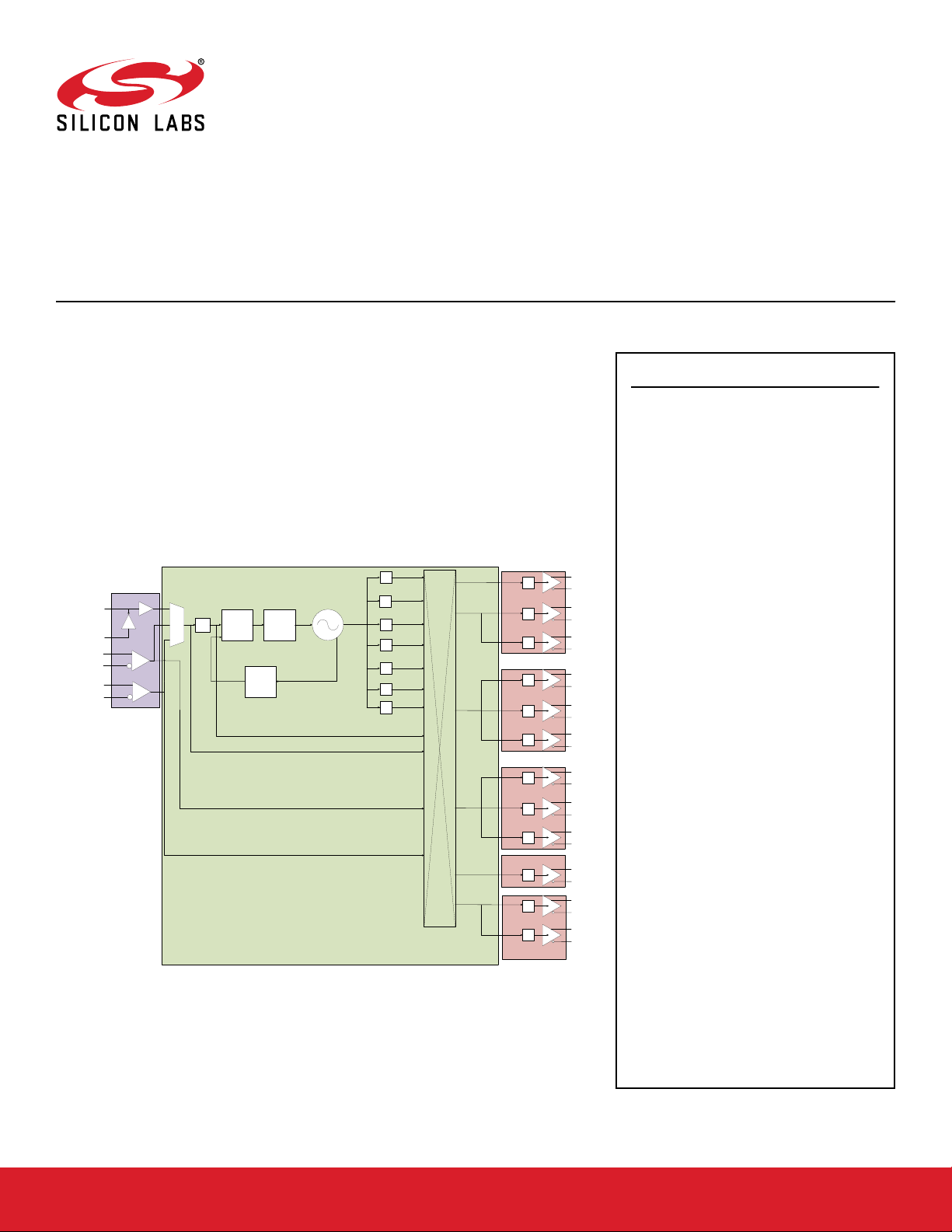
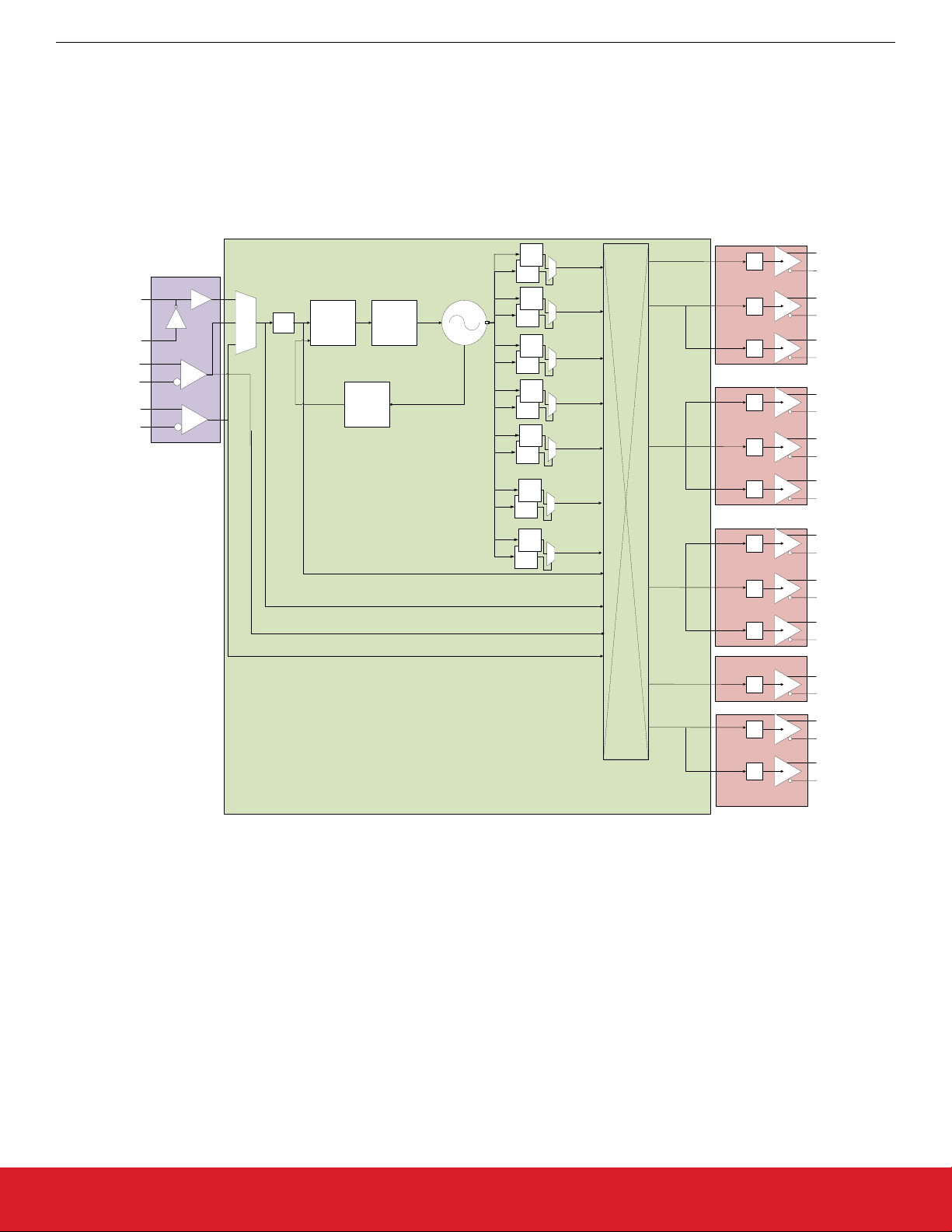
The Si5332-AM1/2/3 is a family of high-performance, low-jitter clock generators capable
of synthesizing five independent banks of user-programmable clock frequencies up to
333.33 MHz, while providing up to 12 differential or 24 single-ended output clocks. The
Si5332 supports free run operation using an external crystal as well as lock to an external clock signal. The output drivers are configurable to support common signal formats,
such as LVPECL, LVDS, HCSL, and LVCMOS. Separate output supply pins allow supply
voltages of 3.3 V, 2.5 V, 1.8 V and 1.5 V (CMOS only) to power the multi-format output
drivers. The core voltage supply (VDD) accepts 3.3 V, 2.5 V, or 1.8 V and is independent
from the output supplies (VDDOs). Using its two-stage synthesis architecture and patented high-resolution Multisynth technology, the Si5332 can generate three fully independent/non-harmonically-related bank frequencies from a single input frequency.
÷N
0
XA/CLKIN_1
CLKIN_2
nCLKIN_2
CLKIN_3
nCLKIN_3
VDDA
VDD_XTAL
10-30 MHz
XB
÷ P
1-31
PFD LF
10-50 MHz
÷M
/M
n
d
10-255
2.375-2.625 GHz
10-50 MHz
10-250 MHz
10-250 MHz
10-250 MHz
10-255
8-255
÷N
÷O
÷O
÷O
÷O
÷O
10-250 MHz
1
10-250 MHz
0
10-312.5 MHz
1
10-312.5 MHz
2
10-312.5 MHz
3
10-312.5 MHz
4
10-312.5 MHz
VDDOA
VDDOB
VDDOC
VDDOD
VDDOE
÷R
÷R
÷R
÷R
÷R
÷R
÷R
÷R
÷R
÷R
÷R
÷R
1-63
OUT0
OUT1
OUT2
OUT3
OUT4
OUT5
OUT6
OUT7
OUT8
OUT9
OUT10
OUT11
RELATED DOCUMENTS
• Any-Frequency 6/8/12-output
programmable clock generators
• Offered in three different package sizes,
supporting different combinations of output
clocks and user configurable hardware
input pins
•
32-pin QFN, up to 6 outputs
• 40-pin QFN, up to 8 outputs
• 48-pin QFN, up to 12 outputs
• Multisynth technology enables any
frequency synthesis on any output up to
250 MHz using N dividers.
• Output frequencies up to 333.33 MHz
using O dividers.
• Highly configurable output path featuring a
cross point mux
• Up to three independent fractional
synthesis output paths
• Up to five independent integer dividers
• Down and center spread spectrum
• Input frequency range:
• External crystal: 16 MHz to 50 MHz
• Differential clock: 10 MHz to 250 MHz
• LVCMOS clock: 10 MHz to 170 MHz
• Output frequency range:
• Differential: 5 MHz to 333.33 MHz
• LVCMOS: 5 MHz to 170 MHz
• User-configurable clock output signal
format per output: LVDS, LVPECL, HCSL,
LVCMOS
• Easy device configuration using our
ClockBuilder Pro™ (CBPro™) software
tool available for download from our web
site
• Temperature range: –40 to +105 °C
• Pb-free, RoHS-6 compliant
• For more information, refer to the Si5332
Automotive Grade Data Sheet
silabs.com | Building a more connected world. Preliminary Rev. 0.2
This information applies to a product under development. Its characteristics and specifications are subject to change without notice.
Page 2

Table of Contents
1. Overview .................................
3
2. Power Supply Sequencing ..........................4
3. Input Clocks................................5
3.1 Input Clock Terminations ..........................5
3.1.1 External Crystal ............................5
3.1.2 External Input Clock on XA Input ......................5
3.1.3 External Input Clock on CLKIN_x/CLKIN_x# ..................6
3.2 Calculating Crystal Loading Capacitance .....................8
4. GPIO .................................10
5. Output Clock Terminations .........................11
5.1 DC-Coupled Output Clock Terminations .....................12
5.2 AC-Coupled Output Clock Terminations .....................16
6. Programming the Volatile Memory (Registers) ..................17
6.1 Programming the PLL ...........................18
6.2 Programming the Clock Path .........................21
6.3 Programming the Output Clock Frequency ....................23
6.4 Programming the Output Clock Format ......................25
6.5 Programming for Frequency Select Operations ...................27
6.6 Programming Spread Spectrum ........................28
7. Si5332 Pinout and Package Variant ......................30
8. Recommended Schematic and Layout Practices .................32
9. Register Map Overview ..........................33
9.1 Si5332 Common Registers ..........................34
9.2 Si5332 32-QFN Specific Registers .......................44
9.3 Si5332 40-QFN Specific Registers .......................49
9.4 Si5332 48-QFN Specific Registers .......................55
10. Revision History............................. 64
silabs.com | Building a more connected world. Preliminary Rev. 0.2 | 2
Page 3

Si5332-AM1/2/3 Automotive Grade Device Reference Manual
Overview
1. Overview
In addition to clock generation, the input clocks can bypass the synthesis stage, enabling the Si5332 to be used as a high-performance
clock buffer or a combination of a buffer and a generator. The Multisynth dividers have two sets of divide ratio registers, an A set and a
B set. The active in-use divide ratio can be switched between the A set or B set via external input pin or register control. This feature
allows for dynamic frequency shifting at ppb accuracy for applications such as frequency margining. Similar A set and B set divider
ratios are available for the integer dividers, but the ratios must be integer related. CBPro supports the configuration and use of A and B
divider sets. Spread spectrum is available for any clock output sourced from the Multisynth dividers and is available for use in EMI-
sensitive applications, such as PCI Express. The 2-wire I2C bus can be used to control and configure the Si5332. Alternatively, some
device features can be controlled by an external pin via CBPro configuration of one of more General Purpose I/O (GPIO) pins. Exam-
ples of GPIO pin assigned control are clock input selection, frequency A/B select, spread spectrum enable, output enable, or I2C address select.
silabs.com | Building a more connected world. Preliminary Rev. 0.2 | 3
Page 4
Si5332-AM1/2/3 Automotive Grade Device Reference Manual
Power Supply Sequencing
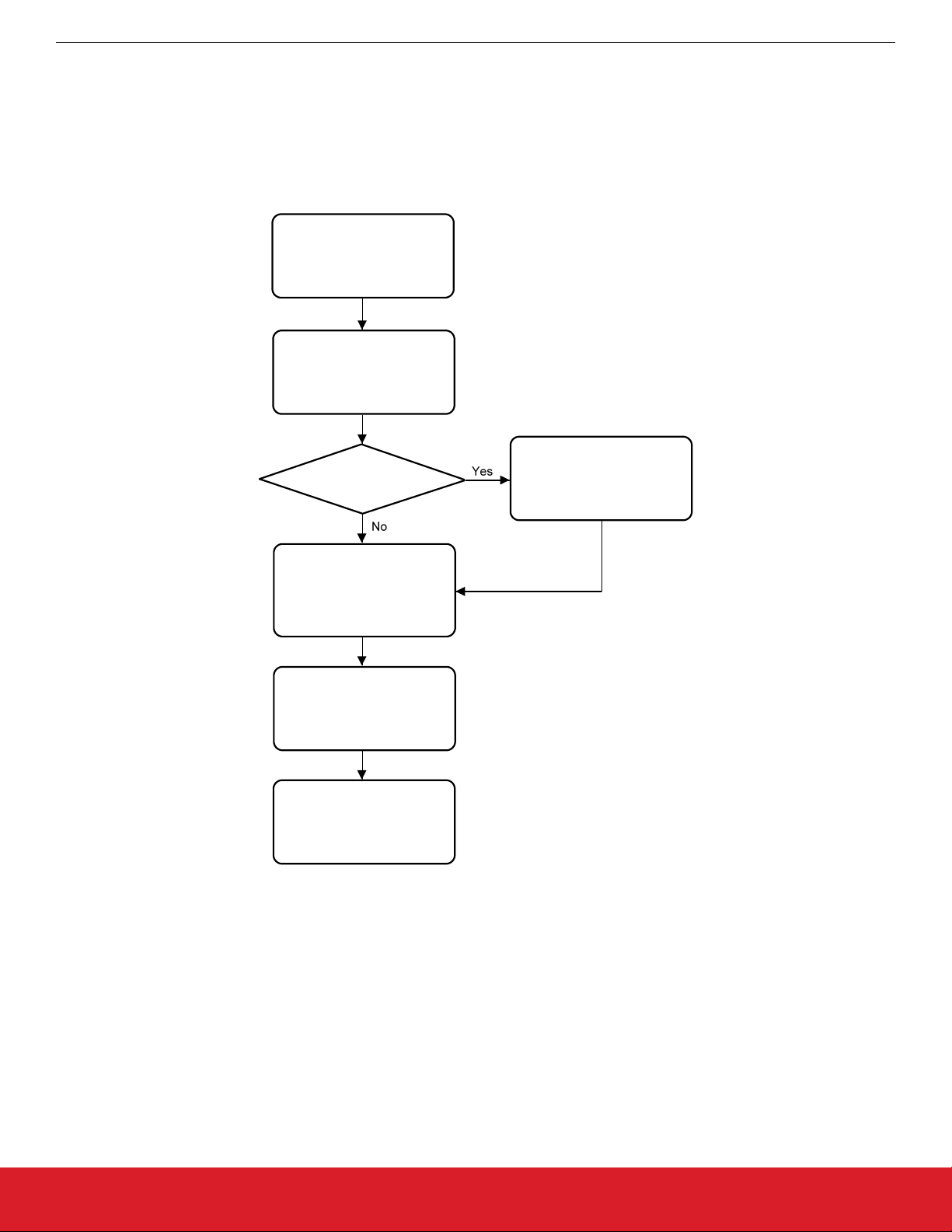
2. Power Supply Sequencing
The Si5332 VDD_core voltages are VDD_DIG, VDD_XTAL, and VDDA. These 3 VDD_core pins must all use the same voltage. Power
supply sequencing between VDD_core and any VDDOx pin is allowed in any order. However, if desiring to minimize the “bring-up” time,
it is recommended that VDD_core is powered up first; this ensures that the NVM download is completed first and the I2C master can
communicate with the Si5332 slave. The figure below shows the Si5332 device power-up sequencing and expected device behavior.
Note that a blank (unconfigured) part will stop and wait to be configured with outputs disabled.
Power supplies for
VDDA, VDD_DIG, and
VDD_XTAL stable
Time (system time delay)
for NVM download
Program Si5332 volatile
Is this a blank part?
memory with a frequency
plan
Time (system time delay)
for Oscillator startup/
Time (system time delay)
for input clock availability
Time (system time delay)
for PLL clock
Outputs available and
stable
Figure 2.1. Power Supply Sequencing for Si5332
silabs.com | Building a more connected world. Preliminary Rev. 0.2 | 4
Page 5
Si5332-AM1/2/3 Automotive Grade Device Reference Manual
Input Clocks
3. Input Clocks
The Si5332 has three input clock nodes: the XA/XB pair, the CLKIN_2/CLKIN_2# pair, and the CLKIN_3/CLKIN_3# pair.
XA/XB supports a crystal input or an external clock input whereas the CLKIN_x/CLKIN_x# pairs support ONLY external clock inputs.
The GPIO pins can be set to select the active input clock for the PLL (or the user can set the active input via register writes).
3.1 Input Clock Terminations
Supported input clock sources for the Si5332 are:
1. External crystal attached to the Si5332 XA/XB inputs.
2. External single-ended clock attached to XA (XA/CLKIN1 pin).
3. Externally supplied clock attached to available CLKIN_x/CLKINx# inputs.
3.1.1 External Crystal
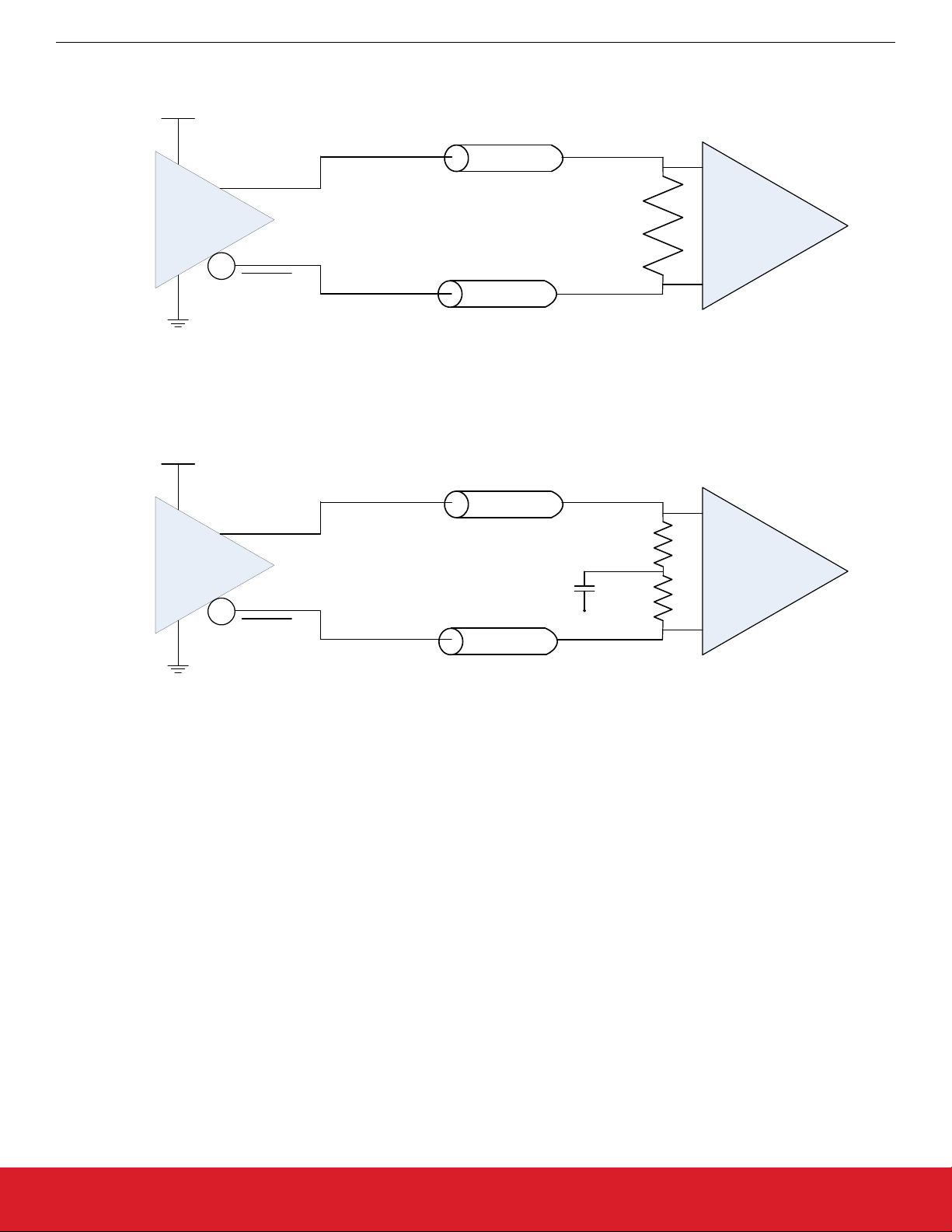
An external crystal can be connected to the Si5332’s XA/XB inputs as shown below. See Table 5.4 in the Si5332 Data Sheet for crystal
specifications when selecting a crystal. Note that the external crystal specifications in Si5332 Data Sheet must be met. A list of recommended AEC-Q200 qualified crystals for the Si5332 can be found in the Silicon Labs document “Recommended Crystal Reference
Manual for Si5332, Si5357, and Si5225x Automotive Grade Clock Generators.”
Figure 3.1. External Crystal Connection
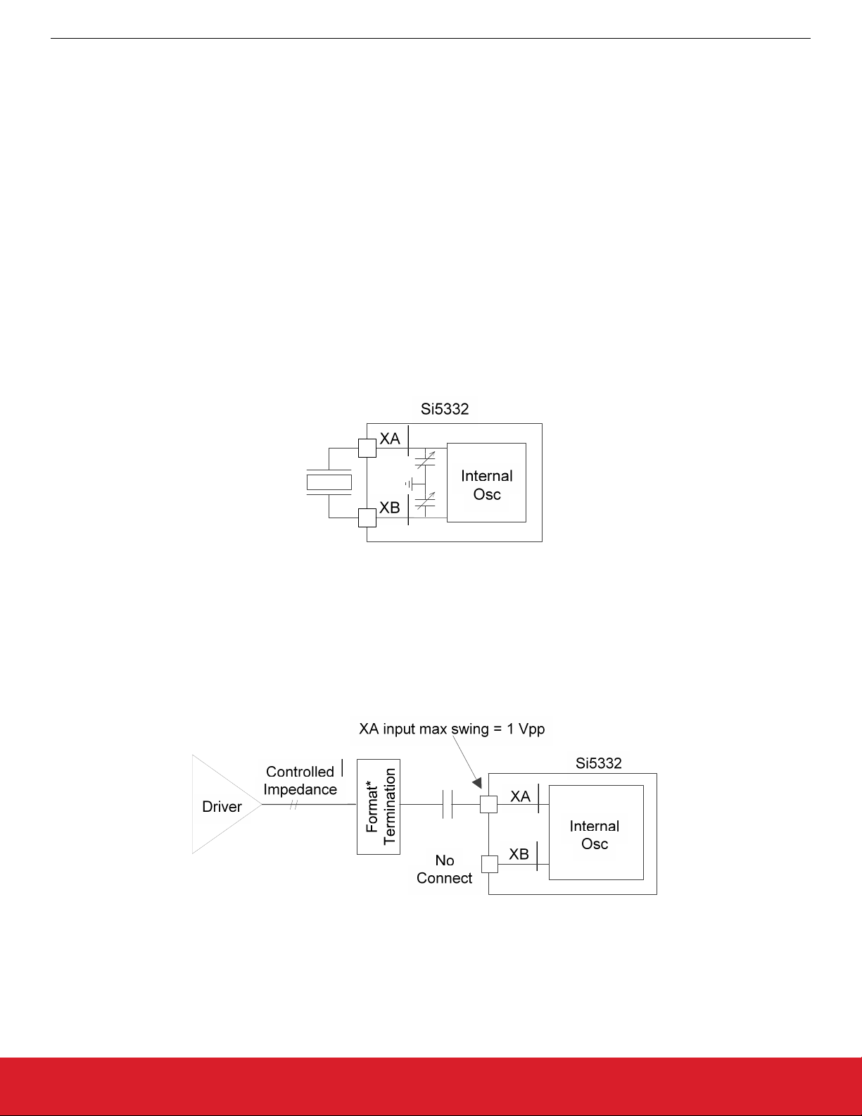
3.1.2 External Input Clock on XA Input
The XA input (XA/CLKIN1 pin) can accept an externally supplied, AC-coupled clock with maximum voltage swing of 1 Vpp. See figure
below for connection details. The XB pin must be left open with nothing connected. If using this input clock mode, it is suggested to zero
out the internal crystal loading capacitance (CL) for best performance.”
0.1 µF
Figure 3.2. External Input Clock on XA Input
silabs.com | Building a more connected world. Preliminary Rev. 0.2 | 5
Page 6
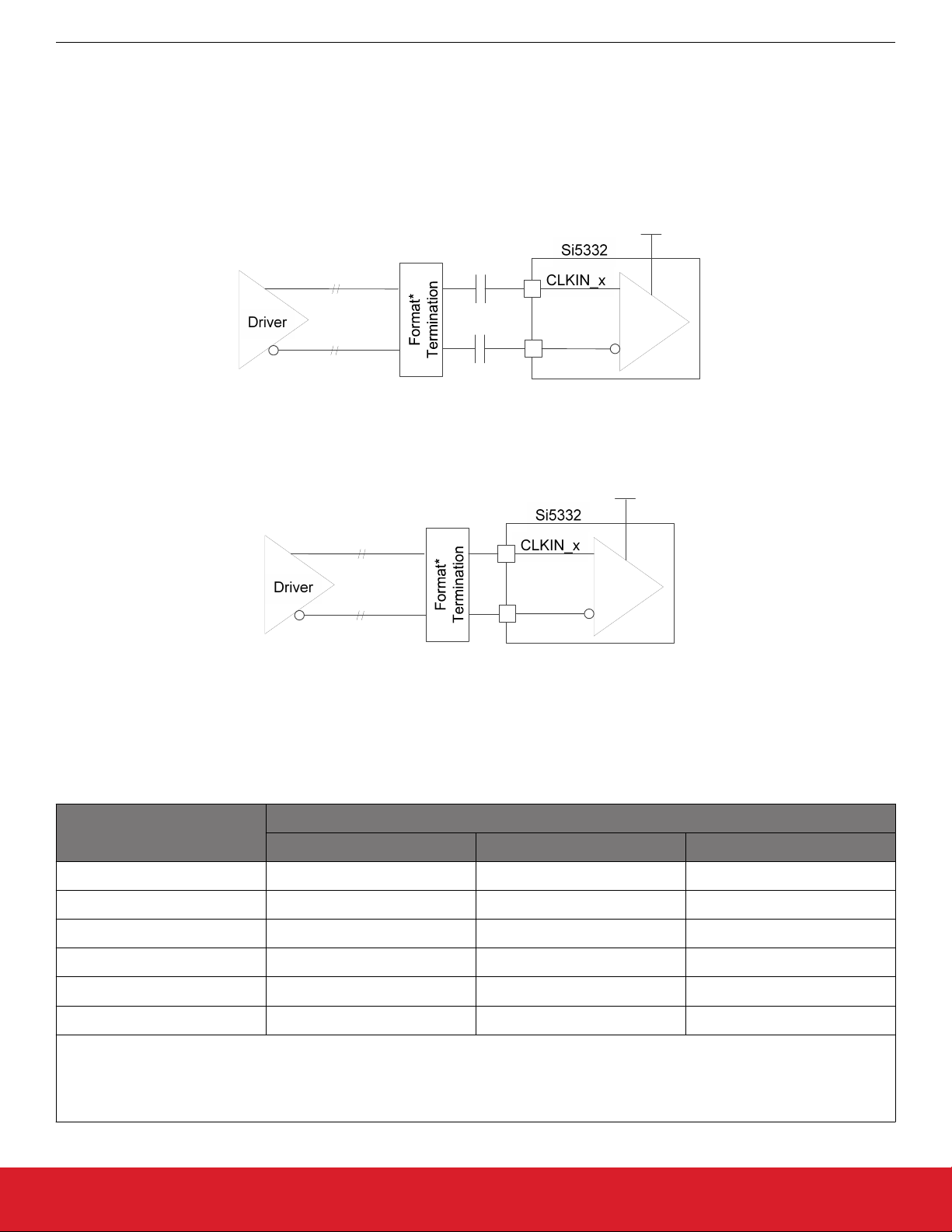
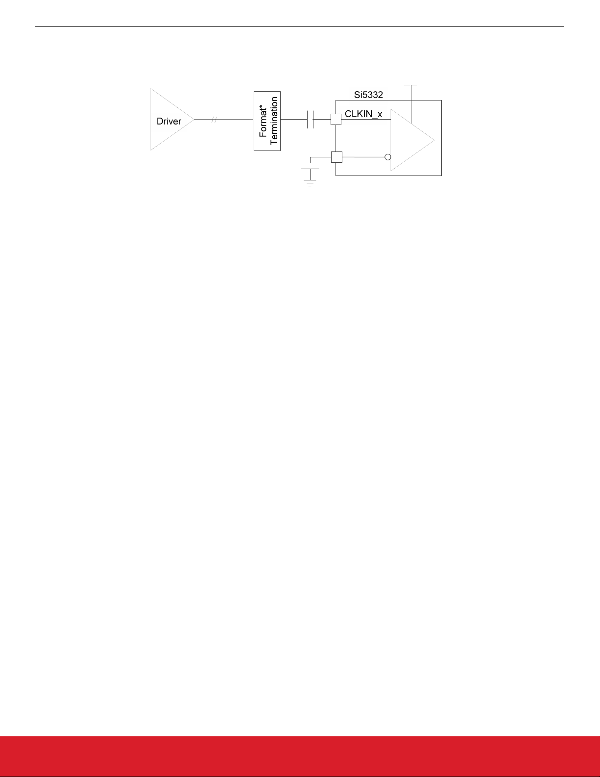
3.1.3 External Input Clock on CLKIN_x/CLKIN_x#
Si5332-AM1/2/3 Automotive Grade Device Reference Manual
Input Clocks
When supplying
the AC and DC coupled differential input clock connection to the Si5332 clock inputs. (There are some restrictions to observe when
using DC coupled input clocks as described further below.) The input clock Format Termination shown in below figures is dependent on
the driver’s termination requirements. The Si5332 clock inputs are high impedance inputs and the clock driven into the Si5332 must
meet the Si5332 Data Sheet's specified electrical requirements. When using differential input clocks, the respective Si5332 input must
be configured as a differential input using CBPro.
differential input clocks into the CLKIN_x/CLKIN_x# inputs, AC or DC coupling can be used. The figures below show
VDD Core
0.1 µF
Controlled
Impedance
CLKIN_x#
0.1 µF
Figure 3.3. AC-Coupled Differential Input Clock (LVDS, LVPECL, HCSL, CML, etc.)
VDD Core
Controlled
Impedance
Figure 3.4. DC-Coupled Differential Input Clock
To determine if a specific DC-coupled differential input clock arrangement is supported, refer to the table below.
Table 3.1. Si5332 Input Clock Coupling Restrictions (AC or DC)
Format
3.3 V 2.5 V 1.8 V
LVDS 3.3 V/2.5 V AC or DC AC only AC only
LVDS 1.8 V AC or DC AC only AC only
LVPECL 3.3 V/2.5 V AC or DC AC only AC only
HCSL AC or DC AC or DC AC only
CML AC only AC only AC only
LVCMOS AC only AC only AC only
CLKIN_x#
VDD_Core
Note:
1.
For DC-coupled, input clock peak voltage must not exceed VDD_Core and minimum voltage must not be below GND.
For AC-coupled, peak swing must not exceed VDD_Core.
2.
silabs.com | Building a more connected world. Preliminary Rev. 0.2 | 6
Page 7
Si5332-AM1/2/3 Automotive Grade Device Reference Manual
Input Clocks
The figure below shows how to connect single-ended input clocks, such as LVCMOS. The single-ended clock must be connected to the
positive CLKIN input as shown below.
VDD Core
Controlled
Impedance
0.1 µF
CLKIN_x#
0.1 µF
Figure 3.5. AC-Coupled Single-Ended Input Clock (LVCMOS)
For AC-coupled single-ended input clocks (such as LVCMOS) the Vswing of the clock must be limited to the maximum VDD_Core voltage. (VDD_Core is defined as the following group of VDD supply pins: VDD_DIG, VDDA, and VDD_XTAL.) The Input clock format termination is dependent on the driver format used and is usually specified by the driving device and/or industry standard clock format
specification.
For example, in the case of using a LVCMOS input clock, the driving device may recommend a series termination resistor. When using
LVCMOS input clocks the Si5332 input must be configured in LVCMOS mode in CBPro. The single-ended CLKIN input of Si5332 is a
high impedance input.
silabs.com | Building a more connected world. Preliminary Rev. 0.2 | 7
Page 8
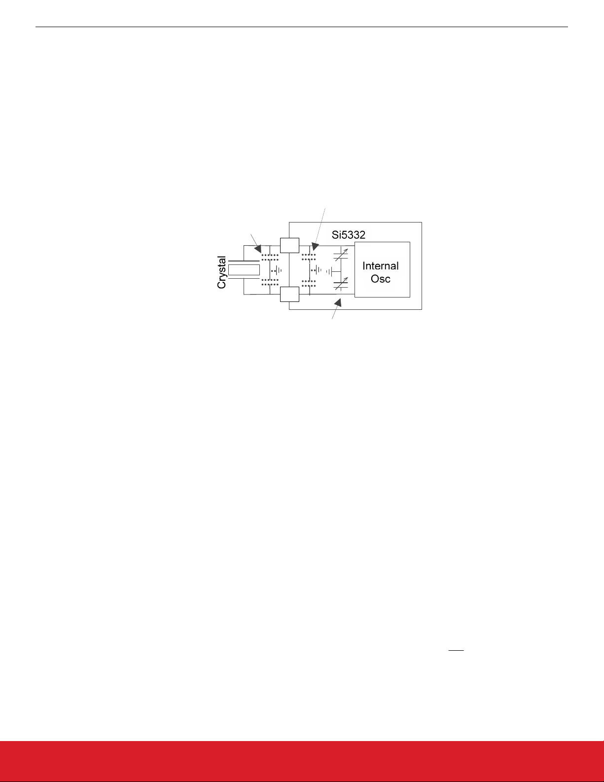
3.2 Calculating Crystal Loading Capacitance
Si5332-AM1/2/3 Automotive Grade Device Reference Manual
Input Clocks
Crystals will
resonate at their specified frequency (i.e., be “on-frequency”) if the capacitive loading across the crystal’s terminals is the
same as specified by the crystal manufacturer’s loading capacitance (CL) specification. The total loading capacitance presented to the
crystal must factor in all capacitance sources such as parasitic “stray” capacitance as well as added loading capacitance. Stray capacitance comes from sources like PCB traces, capacitive coupling to nearby components, as well as any stray capacitance within the device itself. For “on-frequency” oscillator operation, all capacitance sources must be factored into determining the correct additional capacitance to be presented to the crystal to match its required CL.
The Si5332 contains variable internal loading capacitors (CL
) to provide the necessary added crystal matching capacitance such
VAR
that external matching capacitors are not needed. The figure below shows the Si5332’s internal variable capacitance and the two main
sources of stray loading capacitance, PCB stray (CLS
) and Si5332 device stray capacitance on XA/XB input pins (CLS
EXT
INT
).
Internal Stray
Capacitance CLS
INT
External Stray
Capacitance
CLS
EXT
XA
XB
Internal Variable
Capacitance
CL
AR
V
Figure 3.6. Sources of Crystal Loading Capacitance
Using the Si5332’s internal variable loading capacitors (CL
external stray (CLS
) and internal device capacitance (CLS
EXT
), the crystal’s required CL can be matched by adding capacitance to the
VAR
) to match the crystal’s requirements. A value for CL
INT
must be se-
VAR
lected such that:
quired Crystal CL = CL
e
R
VAR
+ CL S
+ CL S
INT
EXT
Or rearranged:
= C
ry
C L
AR
V
stal CL − CL S
Note: the required Crystal CL must be greater than or equal to the total stray capacitance quantity (CLS
can’t be used as CL
is always >= 0.
VAR
− CL S
T
IN
EXT
+ CLS
INT
Equation 1
) or the crystal
EXT
For the following example, a Crystal CL value of 10 pf will be used. The internal stray capacitance (CLS
) of the Si5332 is 2.4 pf.
INT
External PCB stray capacitance (CLSEXT) is usually in the order of 2-3 pf given a reasonably compact layout. The Si5332 EVB external stray capacitance is ~ 2.75 pf. Given these example values, the required CL
can be calculated as shown below, using Equation
VAR
1.
C L
= 10 pF − 2.4 pF − 2.75 p
R
A
V
As shown in the figure above, the internal variable loading capacitor (CL
connected to the XA pin (CLXA) and one to the XB pin (CLXB) of the Si5332. The CL
F = 4.85 pF
implemented by using
) is
VAR
VAR
Using Equation 1
two capacitors in
series: one
value is therefore determined by the values of
CLXA and CLXB .
For capacitors in series, if we keep CLXA = CLXB, we can simply double the value of CL
to arrive at the correct CLXA and CL
VAR
XB
value. (This is a technique commonly used for calculating crystal loading capacitors when external loading capacitors are used.) Now,
CLXA and CLXB values are simply:
silabs.com | Building a more connected world. Preliminary Rev. 0.2 | 8
Page 9

Si5332-AM1/2/3 Automotive Grade Device Reference Manual
Input Clocks
C LXA = C L
Substituting Equation 1 for CL
C LXA = C LXB = 2 ×
Equation 3 can now be used to determine the CLXA and CLXB
of CLXA and CLXB values the Si5332 can support is 0 to 38.395 pF. CLXA and CLXB values less than 0 cannot be implemented and any
values greater than 38.395 pF cannot be implemented using internal capacitors alone. Remember, CLXA and CLXB are not derived simply from the crystal’s CL because internal and external stray capacitance must be factored into the calculations.
Once the required CLXA and CLXB have been determined using Equation 3, use the following set of formulas to calculate the required
register values to implement the desired CLXA and CLXB.
If (CL
• Register xosc_cint_ena = 0
Register xosc_ctrim_xin = Round to nearest integer (CLXA / 0.485)
•
• Register xosc_ctrim_xout = Round to nearest integer (CLXB / 0.485)
If (30.555 pF < CL
• • Register xosc_cint_ena = 1
•
Register xosc_ctrim_xin = Round to nearest integer ((CLXA - 7.84) / 0.485)
• Register xosc_ctrim_xout = Round to nearest integer (CLXB - 7.84) / 0.485)
To summarize, use Equation 3 to calculate CLXA/CLXB, then use the above set of formulas to calculate register values to implement
CLXA/CLXB in the Si5332. Note that external loading capacitors can be used to supplement the internal loading capacitors if necessary.
< 30.555 pF, then:
XA/XB
< 38.395 pF, then:
XA/XB
=
2 × C L
X
VAR
B
(
into Equation 2 will solve for CLXA/CLXB in single equation form:
= 2 × 4.85 pF = 9.7 pF
)
R
VA
Crystal CL − C L
(
values needed to set internal CLXA and CLXB register values. The range
− C L
t
in
ext
Equation 2
)
Equation 3
Note: Your unique PCB assembly’s stray capacitance value plays a role in determining correct internal capacitor settings and, conse-
quently, the crystal’s frequency of oscillation. Small differences in actual board stray capacitance value from the value you use in the
above equations will result in the crystal oscillating slightly off-frequency. Significant capacitance differences can result in significant
frequency error.
silabs.com | Building a more connected world. Preliminary Rev. 0.2 | 9
Page 10

Si5332-AM1/2/3 Automotive Grade Device Reference Manual
GPIO
4. GPIO
Si5332 features universal General Purpose Input/Output (GPIO) hardware pins whose functions must be programmed in NVM to assume a pre-defined function in ClockBuilder Pro during custom configuration file development.
Table 4.1. Available GPIO Pin Functions
Function Name In/Out Description
OEn (up to 7) In Output enable(s) for selected output(s).
SSENn (up to 2) In Spread spectrum enable for outputs derived from N0 / N1 divider.
FSn (up to 7) In Frequency select(s) for Dividers N0, N1, O0-O4.
CLKIN_SEL [1:0] In Input clock select pins (requires use of 2 GPIOs).
Use to add 1 to I2C device base address but is logically Or’ed with I2C ad-
I2C_ADDR0 In
dress bit 0. If device I2C base address is even, assertion will add 1 to base
address. If device I2C base address is odd, assertion or de-assertion will
not change base address.
LOS Out
RESET In
FOOF Out Fast Out Of Frequency (FOOF) signal indicates PLL is not tracking input
Note: Creation of,
(OPN) generated through CBPro and then either factory programmed, or field programmed using the CBPro Field Programming Dongle. GPIO pin functionality can be evaluated/tested on a Si5332 EVB by downloading a valid CBPro configuration into the EVB, and
asserting the GPIO pins on the EVB. New GPIO configurations, or changes to existing GPIO configurations, are not available through
Si5332 I2C register programming. Blank Si5332 devices have no GPIO configuration loaded and require burning a configuration into
device NVM with the Field Programming Dongle to configure any GPIO functionality.
CBPro will allow user configuration of the available GPIOs according to the functionality restrictions of the function selected. Some functions can share a pin, some can not. For example, a single pin can control OE of one or more outputs. Some functions require two pins,
such as CLKIN_SEL0 and CLKIN_SEL1. Some functions are mutually exclusive, for instance FS_x functions can’t share a pin with OE.
For all Si5332 devices, CBPro uses a default I2C base address of 6Ah unless the base address is changed by the user.
or changes to, device GPIO pin functionality is only available when using customized Si5332 orderable part numbers
Loss of Input Clock Signal (Input clock or xtal), active low
put. Requires external pull-up resistor to VDD_CORE.
Device reset, active high input.
reference. FOOF is an active-low open-drain output. Requires external
pull-up resistor to VDD_CORE.
open drain out-
silabs.com | Building a more connected world. Preliminary Rev. 0.2 | 10
Page 11
Si5332-AM1/2/3 Automotive Grade Device Reference Manual
Output Clock Terminations
5. Output Clock Terminations
The Si5332 supports output formats of LVCMOS, LVDS, LVPECL, and HCSL with some additional format specific features. Each output driver is individually programmable to any of the supported formats by use of the following registers.
Table 5.1. Output Format Related Register Fields
outx_mode: - Sets the mode of the driver. See Table 5.2 OUTx_Mode vs Output Formats on page 11
outx_cmos_inv: - Sets the inversion state of each side of the dual output driver when in CMOS driver format.
outx_cmos_slew: - Sets the slew rate of the CMOS driver.
outx_cmos_str: - Sets the output impedance of the CMOS driver (25Ω / 50Ω).
.
Table 5.2. OUTx_Mode vs Output Formats
OUTx_MODE Driver Mode
0 off
1 CMOS on positive output only
2 CMOS on negative output only
3 dual CMOS outputs
4 2.5V/3.3V LVDS
5 1.8V LVDS
6 2.5V/3.3V LVDS fast
7 1.8V LVDS fast
8 HCSL 50 Ω (external termination)
9 HCSL 50 Ω (internal termination)
10 HCSL 42.5 Ω (external termination)
11 HCSL 42.5 Ω (internal termination)
12 LVPECL
13 Reserved
14 Reserved
15 Reserved
The recommended termination for each output format is shown in these figures: Figure 5.1
12 and Figure 5.2 LVCMOS Termination, Option 2 on page 12.
LVCMOS Termination, Option 1 on page
silabs.com | Building a more connected world. Preliminary Rev. 0.2 | 11
Page 12
5.1 DC-Coupled Output Clock Terminations
1.43 V to 3.46 V
Set output driver
to 50 Ω mode.
Figure 5.1. LVCMOS Termination, Option 1
Si5332-AM1/2/3 Automotive Grade Device Reference Manual
Output Clock Terminations
Zo = 50 Ω
OUTx
Zo = 50 Ω
OUTx
1.43 V to 3.46 V
Set output driver
to 25 Ω mode.
Zo = 50 Ω
OUTx
Rs
Zo = 50 Ω
OUTx
Rs
Rs = Zo - Rdrv
Figure 5.2. LVCMOS Termination, Option 2
silabs.com | Building a more connected world. Preliminary Rev. 0.2 | 12
Page 13
1.71 V to 3.46 V
Si5332-AM1/2/3 Automotive Grade Device Reference Manual
Output Clock Terminations
LVDS
driver
1.71 V to 3.46 V
LVDS
driver
OUTx
OUTx
OUTx
OUTx
Zo = R
Zo = R
Figure 5.3. LVDS/LVDS Fast Termination, Option 1
Zo = R
Zo = R
/2
T
/2
T
/2
T
/2
T
R
R
R
T
/2
T
/2
T
LVDS
receiver
LVDS
receiver
Figure 5.4. LVDS/LVDS Fast Termination, Option 2
silabs.com | Building a more connected world. Preliminary Rev. 0.2 | 13
Page 14
Si5332-AM1/2/3 Automotive Grade Device Reference Manual
Output Clock Terminations
2.25 V to 3.46 V
2.25 V to 3.46 V
LVPECL
driver
VDD Standard Resistance Resistance Value
OUTx
OUTx
R1
Zo = 50 Ω
Zo = 50 Ω
R2
Figure 5.5. LVPECL Termination, Option 1
Table 5.3. LVPECL Termination, Option 1
R1
LVPECL
receiver
R2
2.5
3.3
2.25 V to 3.46 V
LVPECL
driver
OUTx
OUTx
R1 250
R2 62.5
R1 125
R2 84
Zo = 50 Ω
R3
Zo = 50 Ω
Figure 5.6. LVPECL Termination, Option 2
R1
LVPECL
receiver
R2
silabs.com | Building a more connected world. Preliminary Rev. 0.2 | 14
Page 15
Si5332-AM1/2/3 Automotive Grade Device Reference Manual
Output Clock Terminations
Table 5.4. LVPECL Termination, Option 2
VDD Standard Resistance Resistance Value
R1 50
2.5
3.3
1.71 V to 3.46 V
HCSL
driver
OUTx
OUTx
R2 50
R3 29.5
R1 50
R2 50
R3 54 or 0
Zo = 42.5 Ω
or 50 Ω
HCSL
receiver
Zo = 42.5 Ω
or 50 Ω
1.71 V to 3.46 V
HCSL
driver
OUTx
OUTx
Figure 5.7. HCSL Internal Termination Mode
Zo = 42.5 Ω
R
= Zo
T
or 50 Ω
Zo = 42.5 Ω
or 50 Ω
= Zo
R
T
Figure 5.8. HCSL External Termination Mode
HCSL
receiver
silabs.com | Building a more connected world. Preliminary Rev. 0.2 | 15
Page 16
5.2 AC-Coupled Output Clock Terminations
Si5332-AM1/2/3 Automotive Grade Device Reference Manual
Output Clock Terminations
1.71 V to 3.46 V
HCSL
driver
1.71 V to 3.46 V
HCSL
driver
Zo = 42.5 Ω
or 50 Ω
OUTx
R
= Zo
T
Zo = 42.5 Ω
or 50 Ω
OUTx
= Zo
R
T
Figure 5.9. HCSL External Termination Mode
Zo = 42.5 Ω
or 50 Ω
OUTx
Zo = 42.5 Ω
or 50 Ω
OUTx
0.1 µF
HCSL
receiver
0.1 µF
0.1 µF
HCSL
receiver
0.1 µF
Figure 5.10. HCSL Internal Termination Mode
1.71 V to 3.46 V for LVDS
Zo = 50 Ω
0.1 µF
OUTx
LVPECL
or LVDS
driver
100 Ω
LVPECL
or LVDS
receiver
Zo = 50 Ω
OUTx
Figure 5.11. LVDS Termination
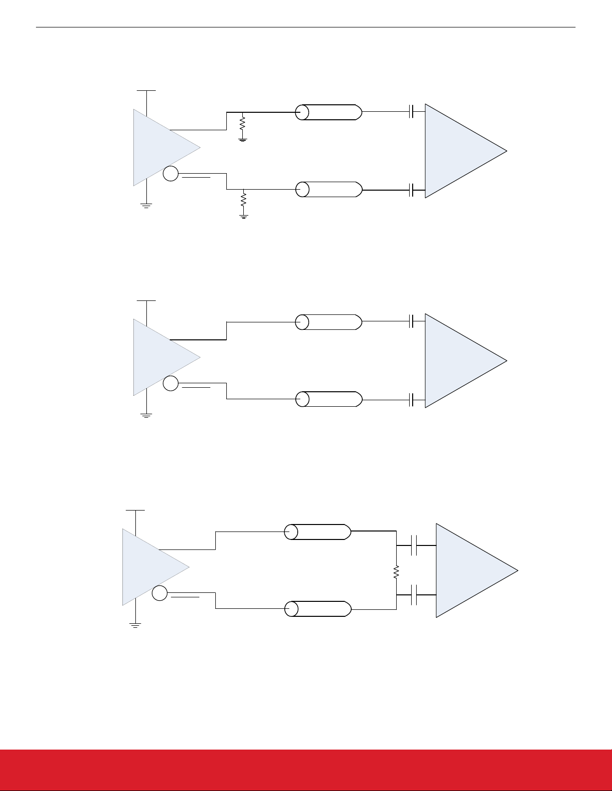
The terminations shown in Figure 5.3 LVDS/LVDS Fast Termination, Option 1 on page 13 through Figure 5.6 LVPECL Termination,
Option 2 on page 14 can also be converted by adding DC-blocking capacitances right before the receiver pins. However, the recom-
mendation shown in Figure 5.11 LVDS Termination on page 16 is the simplest way to realize AC-coupling (i.e., the least number of
components) and the recommended circuit for AC-coupled termination circuits.
0.1 µF
silabs.com | Building a more connected world. Preliminary Rev. 0.2 | 16
Page 17
Si5332-AM1/2/3 Automotive Grade Device Reference Manual
Programming the Volatile Memory (Registers)
6. Programming the Volatile Memory (Registers)
The process described in this section is very complex to implement and/or calculate. A device register solution is most easily calculated
using CBPro and then exporting the resulting register file to simply download into the device. Using CBPro to craft your register set-
ting solution is the most highly recommended approach. The following descriptions of register value calculations are for reference
only.
The volatile memory can be programmed to set up the various functions necessary to realize a PLL function, a clock output to clock
input relationship and can be used to monitor input clock that controls the PLL. The top-level block diagram is repeated here to refresh
the various limits and possibilities that are necessary for the calculations below.
÷N
0a
÷N
0b
÷N
1a
÷N
1b
÷O
0a
÷O
0b
÷O
1a
÷O
1b
÷O
2a
÷O
2b
VDDOA
VDDOB
÷R
÷R
÷R
÷R
÷R
OUT0
OUT1
OUT2
OUT3
OUT4
XA/CLKIN_1
XB
CLKIN_2
nCLKIN_2
CLKIN_3
nCLKIN_3
VDD_XTAL
VDDA
÷ P
PFD LF
÷M
/M
n
d
÷O
3a
÷O
3b
÷O
4a
÷O
4b
Figure 6.1. Top-Level Block Diagram
VDDOC
VDDOD
VDDOE
÷R
÷R
÷R
÷R
÷R
÷R
÷R
1-63
OUT5
OUT6
OUT7
OUT8
OUT9
OUT10
OUT11
silabs.com | Building a more connected world. Preliminary Rev. 0.2 | 17
Page 18
Si5332-AM1/2/3 Automotive Grade Device Reference Manual
Programming the Volatile Memory (Registers)
6.1 Programming the PLL
The PLL programming involves three distinct constraints:
1. The minimum
frequency that sets the input divider P and the active input clock as selected by the IN SEL pins or registers.
2. The VCO frequency that is set by feedback divider (Mn/Md) and the PFD frequency also has a limited range that is unique to
Si5332.
3. The PLL closed loop transfer function characterized by its loop band width and peaking is set by programming the loop parameters.
The table below lists the constraints for the PLL reference frequency and the VCO frequency. The PLL reference frequency
(pllRefFreq) and the VCO frequency (vcoFreq) are related by the equation below:
For a given plan, the pllRefFreq can be readily solved as it is derived from the input clock frequency. To get to this optimization, the
“active” input to the PLL must be selected from the XA/XB, CLKIN_1, CLKIN_2, in 1 p/m input clocks using either the IMUX_SEL register field or the CLKIN_SEL pins (if CKIN_SEL pins are available in the custom part that was chosen to reprogrammed). PllRefFreq is
given by the In-Freq (active clock input frequency) and P as:
and the maximum frequencies possible for the PFD (Phase Frequency Detector) at lock. This is set by the reference
v
coFreq = pllRefFreq ×
RefFreq =
Pll
InFreq
Mn
(
)
Md
P
Table 6.1. Constraints for PLL Reference Frequency and VCO Frequency
Field Name Value Description
pllMinRefFreq 10 MHz The minimum reference frequency the PLL can tolerate
pllMaxRefFreq 50 MHz The maximum reference frequency the PLL can tolerate
vcoCenterFreq 2.5 GHz The center frequency of the VCO’s tuning range
vcoMinFreq 2.375 GHz The minimum frequency of the VCO’s tuning range
vcoMaxFreq 2.675 GHz The maximum frequency of the VCO’s tuning range
List all required output frequencies, Fxy, in groups denoted by Gx, where x = 0,1,2,3,4,5 and y = a,b,c. This grouping is done such that
frequencies related
to each other by rational fractions of integers between 1 and 63 are in that group. For example, 100 MHz/80 MHz =
5/4 is a rational fraction. Each group Gx is associated with a single output voltage supply driver inside Si5332 and is shown in Table
6.2 Output Frequency Variables Grouping and Mapping to Actual Output Pins on page 18. The table also shows the output frequency
symbol Fxy mapped to the output name in the Si5332 pin descriptions. The integer O-dividers are denoted by hsdiv. Each Oi divider
maps to a hsdivi in the solver where i is an integer between 0 and 4. Similarly, the two Multisynth N-dividers, Nj map to IDj and j = 0 or
1. The constraints for these divider values are listed in Table 6.3 Constraints for hsdiv and id on page 19.
Table 6.2. Output Frequency Variables Grouping and Mapping to Actual Output Pins
Si5332 12-Output Part
Output Pair
Si5332 8-Output Part
Output Pair
Si5332 6-Output Part
Output Pair
Output Frequency
Variable for Solver
The Output Frequency
Group
(Future Device)
OUT0 OUT0 OUT0 F
OUT1 OUT1 OUT1 F
OUT2 F
OUT3 OUT2 OUT2 F
OUT4 OUT3 F
OUT5 F
OUT6 OUT4 OUT3 F
silabs.com | Building a more connected world. Preliminary Rev. 0.2 | 18
0A
1A
1B
2A
2B
2C
3A
G
0
G
1
G
1
G
2
G
2
G
2
G
3
Page 19
Si5332-AM1/2/3 Automotive Grade Device Reference Manual
Programming the Volatile Memory (Registers)
Si5332 12-Output Part
Output Pair
(Future Device)
OUT7 OUT5 F
OUT8 F
OUT9 OUT6 OUT4 F
OUT10 OUT7 OUT5 F
OUT11 F
Field Name Value Description
hsdivMinDiv 8 The minimum divide value that the HSDIV can support
hsdivMaxDiv 255 The maximum divide value that the HSDIV can support
idMinDiv 10 The minimum divide value that the ID can support
idMaxDiv 255 The maximum divide value that the ID can support
Each output frequency Foutxy is given by:
Si5332 8-Output Part
Output Pair
Si5332 6-Output Part
Output Pair
Table 6.3. Constraints for hsdiv and id
Output Frequency
Variable for Solver
3B
3C
4A
5A
5B
The Output Frequency
Group
G
3
G
3
G
4
G
5
G
5
For the integer dividers (O0 – O4):
outxy =
F
For the fractional dividers (N0, N1):
utxy =
Fo
or N
An hsdiv
PllRefFreq that satisfies the constraints in Table 6.4 Loop BW Options on page 20. The search for VcoFreq can be broken down into
the following steps:
1. From the output frequency set, form a set of “M” non-equal frequencies. Group the (N-M) equal frequencies into the same “x” in
Foutxy grouping
2. Now form MC2 groups of {M-2} output frequencies. Find the LCM of each group and find an integer “I” that can such that:
a. vcoFreq = I*LCM can meet the constraint for vcoFreq in Table 6.1 Constraints for PLL Reference Frequency and VCO Fre-
b. List the “L” groups that provide a legal vcoFreq, i.e., a vcoFreq that satisfies the condition in step a.
Given that vcoFreq, calculate the fractional feedback divider as:
The Mn/Md
divider is common for output frequencies grouped in a given Gx. Given these constraints, the solver must first choose a
quency.
c. Choose the vcoFreq that has most number of performance critical clocks that do not need “spread spectrum” clocking as part
of the “M-2” output clocks.
Mn
=
Md
fraction is represented in register fields IDPA_INTG, IDPA_RES and IDPA_DEN
ID
PA_INTG = floor
vcoFreq
hsdivj × Rxy
vcoFreq
Nxj × Rxy
vcoFreq
pllRefFreq
128 × vcoFreq
(
pllRefFreq
)
IDPA_RES
IDPA_DEN
As can be seen from the above equations, the ratio IDPA_RES/ IDPA_DEN will always be less than 1.
silabs.com | Building a more connected world. Preliminary Rev. 0.2 | 19
128 × vcoFreq
=
(
pllRefFreq
– IDPA_INTG
)
Page 20
Si5332-AM1/2/3 Automotive Grade Device Reference Manual
Programming the Volatile Memory (Registers)
Note: All these register fields are 15 bits wide. Therefore, the fraction will need to truncate up to this precision. This section fully deter-
the VCO frequency, the P-divider and the feedback divider for this plan given the choice of using O-dividers {HSDIV} for M-2
mines
output clocks and N-dividers {ID} for two output clocks.
The next step will be to determine the closed loop response that is required from the PLL. The table below lists the different loop BW
settings possible and the register field value that will enable that loop BW setting:
Table 6.4. Loop BW Options
PLL_MODE Loop Bandwidth (kHz) PLL. Ref. Freq. Min (MHz) PLL. Ref. Freq. Max. (MHz)
0 ILLEGAL IF PLL MODE IS ENA-
BLED
1 350 10 15
2 250 10 15
3 175 10 15
4 500 15 30
5 350 15 30
6 250 15 30
7 175 15 30
8 500 30 50
9 350 30 50
10 250 30 50
11 175 30 50
This algorithm will result in a final solution for a VCO frequency, vcoFreq, that can then be used to calculate the O-divider, N-divider,
and R-divider values needed to derive each output frequency, Foutxy.
silabs.com | Building a more connected world. Preliminary Rev. 0.2 | 20
Page 21

6.2 Programming the Clock Path
Si5332-AM1/2/3 Automotive Grade Device Reference Manual
Programming the Volatile Memory (Registers)
Given a
valid VCO frequency for the M unique frequencies, segregate the N-M equal frequencies into outputs from each group Gx in
Table 6.2 Output Frequency Variables Grouping and Mapping to Actual Output Pins on page 18. When arranging outputs, care must be
taken to minimize crosstalk (without violating the constraints imposed from the grouping of output frequencies into the VDDO “banks”).
Whenever several high frequencies, fast rise time, large amplitude signals are all close to one another, the laws of physics dictate that
there will be some amount of crosstalk. The jitter of the Si5332 is low, and, therefore, crosstalk can become a significant portion of the
final measured output jitter. Some of the source of the crosstalk will be the Si5332 and some will be introduced by the PCB. For extra
fine tuning and optimization in addition to following the usual PCB layout guidelines, crosstalk can be minimized by modifying the arrangements of different output clocks:
1. Avoid adjacent frequency values that are close. A 155.52 MHz clock should not be next to a 156.25 MHz clock. If the jitter integration bandwidth goes up to 20 MHz, then keep adjacent frequencies at least 20 MHz apart.
2. Adjacent frequency values that are integer multiples of one another are okay and these outputs should be grouped accordingly.
3. Unused outputs can be used to separate clock outputs that might otherwise interfere with one another. If some outputs have tight
jitter requirements while others are relatively loose, rearrange the clock outputs so that the critical outputs are the least susceptible
to crosstalk. These guidelines typically only need to be followed by those applications that wish to achieve the highest possible
levels of jitter performance. Because CMOS outputs have large pk-pk swings and do not present a balanced load to the VDDO
supplies, CMOS outputs generate much more crosstalk than differential outputs. For this reason, CMOS outputs should be avoided
whenever possible. When CMOS is unavoidable, even greater care must be taken with respect to the above guidelines.
An output multiplexer (output mux) or crosspoint mux needs to be programmed such that each group Gx is set to the correct O-divider,
N-divider, or input clock (in the case of buffering). Each output, Foutxy, has this common divider or input clock reference that needs to
be set. The multiplexer setting that routes the correct divider/clock source to the correct group is shown in the following table.
Table 6.5. Output Mux (Crosspoint Mux) Settings
Register Field Description
Selects output mux clock for output clocks in group Gx:
0 = PLL reference clock before pre-scaler
omuxx_sel0
1 = PLL reference clock after pre-scaler
2 = Clock from input buffer 0
3 = Clock from input buffer 1
Selects output mux clock for output clocks in group Gx:
0 = HSDIV0
1 = HSDIV1
2 = HSDIV2
omuxx_sel1
3 = HSDIV3
4 = HSDIV4
5 = ID0
6 = ID1
7 = Clock from omux1_sel0
The final steps will be to program the hsdiv and id (N)
dividers. The equations below show the relationship between hsdiv, id divider
values with their associated output frequency. They also show the register fields that need to be programmed to set up the divider values correctly. The register field and the divider value are both denoted by:
divxa_div =
hs
vcoFreq
Foutxa × Rxa
The id (i.e. N) dividers are calculated as below:
xa =
id
silabs.com | Building a more connected world. Preliminary Rev. 0.2 | 21
vcoFreq
Foutxa × Rxa
Page 22

Si5332-AM1/2/3 Automotive Grade Device Reference Manual
Programming the Volatile Memory (Registers)
The ida fraction is represented in register fields IDPA_INTG, IDPA_RES and IDPA_DEN:
xA_INTG = floor
ID
128 × vcoFreq
(
Foutxa × Rxa
)
IDxA_RES
IDxA_DEN
128 × vcoFreq
=
(
Foutxa × Rxa
- IDxA_INTG
)
silabs.com | Building a more connected world. Preliminary Rev. 0.2 | 22
Page 23

6.3 Programming the Output Clock Frequency
Si5332-AM1/2/3 Automotive Grade Device Reference Manual
Programming the Volatile Memory (Registers)
The Rxy register
fields are programmed as shown in the table below. This last step completes the settings of all dividers that will result
in the frequency plan. When a valid divider solution space cannot be determined, that frequency plan is not realizable in the Si5332.
Table 6.6. Rxy to Register Field Mapping
Divider Value Register Field Description
Driver divider ratio.
R0A OUT0_DIV
0 = disabled
1–63 = divide value
Driver divider ratio.
R1A OUT1_DIV
0 = disabled
1–63 = divide value
Driver divider ratio.
R1B OUT2_DIV
0 = disabled
1–63 = divide value
Driver divider ratio.
R2A OUT3_DIV
0 = disabled
1–63 = divide value
R2B OUT4_DIV
R2C OUT5_DIV
R3A OUT6_DIV
R3B OUT7_DIV
R3C OUT8_DIV
Driver divider ratio.
0 = disabled
1–63 = divide value
Driver divider ratio.
0 = disabled
1–63 = divide value
Driver divider ratio.
0 = disabled
1–63 = divide value
Driver divider ratio.
0 = disabled
1–63 = divide value
Driver divider ratio.
0 = disabled
1–63 = divide value
Driver divider ratio.
R4A OUT9_DIV
0 = disabled
1–63 = divide value
silabs.com | Building a more connected world. Preliminary Rev. 0.2 | 23
Page 24

Si5332-AM1/2/3 Automotive Grade Device Reference Manual
Programming the Volatile Memory (Registers)
Divider Value Register Field Description
Driver divider ratio.
R5A OUT10_DIV
R5B OUT11_DIV
0 = disabled
1–63 = divide value
Driver divider ratio.
0 = disabled
1–63 = divide value
silabs.com | Building a more connected world. Preliminary Rev. 0.2 | 24
Page 25

6.4 Programming the Output Clock Format
The following tables provide the method to fully define every driver.
Table 6.7. Driver Set Up Options
Driver Register Field Description
Si5332-AM1/2/3 Automotive Grade Device Reference Manual
Programming the Volatile Memory (Registers)
Driver for output OUTx
OUTx_mode
OUTx _skew
OUTx _stop_highz
OUTx _cmos_inv
OUTx _cmos_slew
OUTx _cmos_str
Software interpreted driver configuration. See Table 6.8 Driver
Mode Options
on page 25.
Skew control. Programmed as an unsigned integer. Can add delay of 35 ps/step up to 280 ps.
Driver output state when stopped.
0 = low-z
1 = high-z
Sets the polarity of the two outputs in dual CMOS mode
0 = no inversion
1 = OUTx~ inverted
Controls CMOS slew rate from fast to slow.
00 = fastest
01 = slow
10 = slower
11 = slowest
CMOS output impedance control.
0 = 50 Ω
1 = 25 Ω
Table 6.8. Driver Mode Options
drvxy_MODE Driver Mode
0 off
1 CMOS on positive output only
2 CMOS on negative output only
3 dual CMOS outputs
4 2.5 V/3.3 V LVDS
5 1.8 V LVDS
6 2.5 V/3.3 V LVDS fast
7 1.8 V LVDS fast
8 HCSL 50 Ω (external termination)
9 HCSL 50 Ω (internal termination)
10 HCSL 42.5 Ω (external termination)
11 HCSL 42.5 Ω (internal termination)
12 LVPECL
silabs.com | Building a more connected world. Preliminary Rev. 0.2 | 25
Page 26

Si5332-AM1/2/3 Automotive Grade Device Reference Manual
Programming the Volatile Memory (Registers)
drvxy_MODE Driver Mode
13 Reserved
14 Reserved
15 Reserved
silabs.com | Building a more connected world. Preliminary Rev. 0.2 | 26
Page 27

6.5 Programming for Frequency Select Operations
Si5332-AM1/2/3 Automotive Grade Device Reference Manual
Programming the Volatile Memory (Registers)
Every hsdiv and id
dividers. Any FS frequency will be:
Or
Any output associated with either idxa
divider is as shown in table below.
Register Field Description
hsdivx_div_sel
idx_cfg_sel
has a Bank A and a Bank B divider. The register field names that begin with hsdivxb or idxb denote Bank B
Table 6.9. The Control Register Bit to Switch Frequencies
Selects bank A or bank B divider HSDIV0 settings. The HSDIV0 supports dynamic integer divider
changes through this divider select control bit.
0 = bank A divider
1 = bank B divider
Output interpolative divider 0 configuration bank select. The interpolative divider supports dynamically switching between two complete configurations controlled by this bit. Reconfiguration should
be done on the unselected bank. If ID0_CFG=0, running based off bank A, then bank B may be
freely reconfigured and once ready all changes will be applied to the ID once ID0_CFG=1 thus
changing the ID from bank A to bank B. Spread spectrum enable fields ID0A_SS_ENA and
ID0B_SS_ENA are the only exception and may be enabled/disabled while bank is selected.
or hsdivxa
utx yFS =
Fo
utx yFS =
Fo
can be switched into the above FS frequency. The control that selects the Bank B
vcoFreq
idxb
vcoFreq
hsdivb
0 = bank A
1 = bank B
In a factory-programmed part, a pin (the FS pin) can be used for the same purpose as the control registers. Once a control bit is set, the
backup divider values control the output frequency and that is described by the equations below:
For O-Divider
s
divxb_div =
h
For N-Divider
xb =
id
The ida fraction is represented in register fields IDPB_INTG, IDPB_RES and IDPB_DEN
DxB
_INTG = floor
I
IDxB_RES
IDxB_DEN
As can be seen from the equations above, the backup divider values limit the possible values for the output frequency in this backup
mode. Another
quency updates is to program either divider a or b (when divider b or a is currently driving the output frequency), and then switch this
divider.
key feature is that the switch to a FS frequency is “glitchless”. Therefore, the recommended method for glitchless fre-
=
Foutxb × Rxa
128 × vcoFreq
(
Foutxb × Rxa
vcoFreq
Foutxb × Rxa
vcoFreq
128 × vcoFreq
(
Foutxb × Rxa
- IDxB_INTG
)
)
silabs.com | Building a more connected world. Preliminary Rev. 0.2 | 27
Page 28
6.6 Programming Spread Spectrum
Si5332-AM1/2/3 Automotive Grade Device Reference Manual
Programming the Volatile Memory (Registers)
Spread spectrum
clocking (SSC) is available only on the Multisynth outputs. Each Multisynth can implement spread spectrum in either
the main divider or the backup divider (the FS option). Therefore, the user can program a maximum of four different spread spectrum
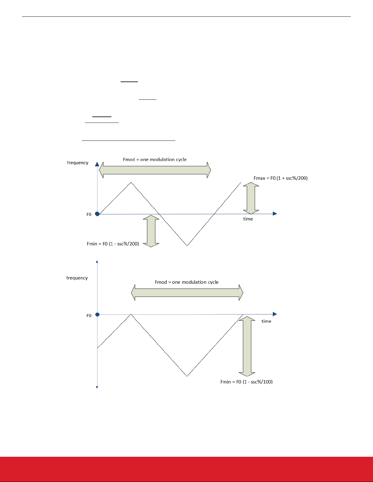
“profiles” from the same part, although only two profile are available on outputs at any given time. The amplitude of the SSC clock frequency (as illustrated in the figure below) is denoted by ssc%. The variable, Amod, in the equation below is a real number
representation of the ssc%, which is a percentage value. The modulation rate (also illustrated in the figure below) is denoted by Fmod
in the equations below.
For Down Spread:
For Center Spread:
idxy_ss_step_num =
idxy_ss_step_res =
Amod =
A
mod = 2 ×
vcoFreq
idxy
Fmod × 4
Amod × idxy_den × idxy × 128
2 × idxy_ss_step_num
ssc %
100
ssc %
100
Figure 6.2. Center and Down Spread SSC Clocks as Frequency vs Time
The table below shows the register fields (and terms) idxy_ss_step_num and idxy_ss_step_res
. idxy_ss_step_num is the number of
frequency steps between the mean and the maximum/minimum frequencies in SSC clocking and idxy_ss_step_res is the frequency
resolution that is required in each step. The goal is to maximize the number of steps and minimize the resolution. However, the number
of steps is set by the modulation rate (typically 30–33 kHz). The step resolution can be minimized by setting the largest value possible
for idxy_den. Idxy_den is the denominator of the id divider and setting it as close as possible to 215 – 1 is desired.
silabs.com | Building a more connected world. Preliminary Rev. 0.2 | 28
Page 29

idxy_ss_ena
Si5332-AM1/2/3 Automotive Grade Device Reference Manual
Programming the Volatile Memory (Registers)
Table 6.10. SSC Register Fields
Spread spectrum enable. This is the only bank configuration field which may be changed dynamically while the bank is selected as the active bank. Users may freely enable/disable spread spectrum.
0 = spread spectrum disabled
1 = spread spectrum enabled
Spread spectrum mode.
0 = disabled
idxy_ss_mode
1 = center
2 = invalid
3 = down
idxy_ss_clk_num Number of output clocks for each frequency step.
idxy_ss_step_num
idxy_ss_step_intg Divide ratio spread step size.
idxy_ss_step_res Numerator of spread step size error term.
idxy_ss_step_den Denominator of spread step size error term.
To enable SSC, idxy_ss_ena needs
Number of frequency steps in one quarter SSC modulation period, allows for frequency step every
output clock.
to be set and the right mode selected in idxy_ss_mode. The number of output clocks in each
frequency step, idxy_ss_clk_num, needs to be set to 1 and idxy_ss_step_den is the same as idxy_den and idxy_ss_step_intg is
always zero.
The following flow needs to be followed to program the registers into Si5332:
1. Write 0x01h to register 0x06h and put the Si5332 into the READY state.
2. Write all the relevant registers as calculated from the steps above.
3. Ensure that the valid input clocks are available for the Si5332 to attempt a PLL lock.
4. Write 0x02h to register 0x06h and put the Si5332 into the ACTIVE state.
silabs.com | Building a more connected world. Preliminary Rev. 0.2 | 29
Page 30

Si5332-AM1/2/3 Automotive Grade Device Reference Manual
Si5332 Pinout and Package Variant
7. Si5332 Pinout and Package Variant
There are three versions of the Si5332 available for customers. The pinout for each is shown in the figures below.
Figure 7.1. 12-Output Si5332 7x7 mm QFN Package
silabs.com | Building a more connected world. Preliminary Rev. 0.2 | 30
Page 31

Si5332-AM1/2/3 Automotive Grade Device Reference Manual
Si5332 Pinout and Package Variant
Figure 7.2. 8-Output Si5332 6x6 mm QFN Package
Figure 7.3. 6-Output Si5332 5x5 mm QFN Package
silabs.com | Building a more connected world. Preliminary Rev. 0.2 | 31
Page 32

Si5332-AM1/2/3 Automotive Grade Device Reference Manual
Recommended Schematic and Layout Practices
8. Recommended Schematic and Layout Practices
The Si5332 schematic and layout design can be referenced from the respective EVB design for Si5332. For each package, the User’s
Guide (links below) outlines the EVB design and provides links to schematic and layout references for each package type.
• UG398: Si5332-8A-EVB User's Guide
• UG397: Si5332-6A-EVB User's Guide
• UG462: Si5332-12A-EVB User’s Guide
At the schematic/placement/layout design time, these are the following guidelines:
1. Power supply filtering:
a. The Si5332 can tolerate up to 100 mV (+/-50 mV) of noise for each supply node. The Application Note, AN1107: Si5332 Pow-
er Supply Noise Rejection, provides the performance to be expected with such a noise.
i. As can be seen, this noise can be from a switched mode power supply (which causes noise over a wide band of frequen-
cies) or can be noise due to some oscillatory behavior from an LDO regulator.
ii. The only filtering needed on each supply node is a 1 μF and a 0.1 μF placed as close as possible to that node.
iii. The Si5332 EVBs have a much larger capacitance on the regulator end, mainly to compensate for the regulator loop so
that there is no oscillatory behavior from the regulators regardless of the voltage supply value set for that regulator. The
regulator supply design on the EVB is not required for Si5332 in system designs.
2. Crystal placement:
a. The crystals should be placed as close as possible to the XA/XB pins. This placement ensures that the crystal oscillator traces
do not cause undue delays and hence, cause either an unusually long crystal start up time or get susceptible to crosstalk and
thereby increase jitter on the output clocks.
silabs.com | Building a more connected world. Preliminary Rev. 0.2 | 32
Page 33

Si5332-AM1/2/3 Automotive Grade Device Reference Manual
Register Map Overview
9. Register Map Overview
All common registers are listed in the table below. The registers that are specific to the 32-QFN part are listed in Si5332 32-QFN Regis-
ters. The registers that are specific to the 40-QFN part are listed in Si5332 40-QFN Registers. The registers that are specific to the 48-
QFN part are listed in Si5332 48-QFN Registers. The fields in these tables are the register field name, address, base, bit length, “R/W/
RW”, description, and device mode. Note that all registers hold values that are "big-endian" (i.e., bit 7 is the MSB in an eight-bit field).
The definitions for these fields are as follows:
1. Register Field Name: The name for the register field in this FRM as referenced in the tables below and in other sections in this
FRM.
2. Address: The 8-bit register address to be used in the I2C transactions when the register field needs to be addressed.
3. Base: Every register field address addresses an 8-bit wide location. However, the register field may not occupy that entire location.
In those cases, they may also not start at the LSB (i.e., bit #0 of that location). Base provides the bit #i from which this register field
begins in the addressed location.
4. Bit Length: Bit length indicates the “number of bits” that the register field occupies in the addressed location.
5. R/W/RW: This field indicates if the register field is Read only (R), Write only (W) or Read/Write (RW).
6. Description: Description is an explanation on the purpose and programmability offered by the register field.
7. Device Mode: Device mode is the mode of Si5332 in which the register field can be accessed. Si5332 has two modes of function
“READY” where the Si5332 is ready for programming in which time there will no outputs from Si5332 and “ACTIVE” where the
Si5332 is actively locked to an input and is providing outputs. Some register fields can be programmed in either READY or ACTIVE
mode (READY/ACTIVE) whereas others can only be programmed in READY mode (READY). Device mode provides input on
which mode applies to a register field a user intends to modify.
silabs.com | Building a more connected world. Preliminary Rev. 0.2 | 33
Page 34

9.1 Si5332 Common Registers
Si5332-AM1/2/3 Automotive Grade Device Reference Manual
Register Map Overview
Table 9.1. Si5332 Register Map
Register Field Name Address Base
Bit
Length
R/W/RW Description Device Mode
VDD_XTAL_OK 5 7 1 R Flag that VDD_XTAL is greater than its min-
imum level, which is about 1.5 V.
VDDO_OK 5 0 6 R Each bit in the VDDO_OK register field indi-
cates a specific VDDO supply is above 1.2
V, with bit position corresponding to VDDO
supply number. Bit 0 is VDDO0 status, Bit 1
is VDDO1 status, Bit 2 is VDDO2 status,
and so on up to Bit 5 is VDDO5 status.
USYS_CTRL 6 0 8 RW User System Control. Use this write-only
register to command the device to transition
to ACTIVE or READY state. (Use
USYS_STAT to read present state.) Writing
0x01 to command device to enter READY
state, write 0x02 to enter ACTIVE state.
USYS_STAT 7 0 8 R User System Status. This read-only register
indicates the present device operational
state. Can be used with USYS_CTRL to
confirm device has entered the commanded
state (i.e., ACTIVE or READY). Reading
0x01 indicates in READY state, 0x02 indicates in ACTIVE state. If 0x89 is read this
indicates device has not detected an input
clock source and can't proceed to ACTIVE
state.
READY/ ACTIVE
READY/ ACTIVE
READY/ ACTIVE
UDRV_OE_ENA 8 0 1 RW User master output enable. Resets to 1.
READY/ ACTIVE
This bit controls simultaneously the driver
start for all drivers.
USER_SCRATCH0 9 0 8 RW
USER_SCRATCH1 A 0 8 RW
User scratch pad registers, freely R/W any
time. This is just run time scratch area, not
READY/ ACTIVE
initialized from NVM. The reset value is
USER_SCRATCH2 B 0 8 RW
USER_SCRATCH3 C 0 8 RW
0x00 for all bytes. Can be I2C read and
written any time.
DEVICE_PN_BASE D 0 8 R Device part number (For CBPro use) READY/ ACTIVE
silabs.com | Building a more connected world. Preliminary Rev. 0.2 | 34
Page 35

Si5332-AM1/2/3 Automotive Grade Device Reference Manual
Register Map Overview
Register Field Name Address Base
Bit
Length
R/W/RW Description Device Mode
DEVICE_REV E 0 8 R Device revision (For CBPro use) READY/ ACTIVE
DEVICE_GRADE F 0 8 R Device grade information (For CBPro use)
FACTORY_OPN_ID0 10 0 4 R The Orderable part number identification,
OPN ID-0.
Example:
For Si5332AD9876
5-AM1, ID-0 = 5.
FACTORY_OPN_ID1 10 4 4 R The Orderable part number identification,
OPN ID-1.
Example:
For Si5332AD987
65-AM1, ID-1 = 6.
FACTORY_OPN_ID2 11 4 4 R The Orderable part number identification,
OPN ID-2.
Example:
For Si5332AD98765-AM1, ID-2 = 7.
FACTORY_OPN_ID3 11 0 4 R The Orderable part number identification,
OPN ID-3.
Example:
For Si5332AD98765-AM1, ID-3 = 8.
FACTORY_OPN_ID4 12 0 4 R The Orderable part number identification,
OPN ID-4.
Example:
For Si5332AD98765-AM1, ID-4 = 9.
FACTORY_OPN_RE-
VISION
DESIGN_ID0 17 0 8 R
DESIGN_ID1 18 0 8 R
12 4 4 R The Orderable part number's product revi-
sion number.
READY/ ACTIVE
Design identification set by user in CBPro
project file
DESIGN_ID2 19 0 8 R
I2C_ADDR 21 0 7 R I2C mode device address. Reset value is
110_1010 binary.
I2C_SCL_PUP_ENA 23 0 1 RW Enable 50 kΩ pullup resistor on SCL pad. READY/ ACTIVE
I2C_SDA_PUP_ENA 23 1 1 RW Enable 50 kΩ pullup resistor on SDA pad. READY/ ACTIVE
OMUX0_SEL0 25 0 2 RW Selects output mux clock source for output
READY/ ACTIVE
clocks in group G0:OUT0 for AM1, AM2:
0 = PLL reference clock before pre-scaler
1 = PLL reference clock after pre-scaler
2 = Clock from input buffer CLKIN_2
3 = Clock from input buffer CLKIN_3
silabs.com | Building a more connected world. Preliminary Rev. 0.2 | 35
Page 36

Si5332-AM1/2/3 Automotive Grade Device Reference Manual
Register Map Overview
Register Field Name Address Base
Bit
Length
R/W/RW Description Device Mode
OMUX0_SEL1 25 4 3 RW Selects output mux clock source for output
clocks in group G0:OUT0 for AM1, AM2:
0 = HSDIV0
1 = HSDIV1
2 = HSDIV2
3 = HSDIV3
4 = HSDIV4
5 = ID0
6 = ID1
7 = Clock from OMUX0_SEL0
Note that the OMUX0_SEL1 value is forced
to 7 whenever the PLL is disabled
OMUX1_SEL0 26 0 2 RW Selects output mux clock source for output
clocks in group G1: OUT1 for AM1, AM2:
0 = PLL reference clock before pre-scaler
1 = PLL reference clock after pre-scaler
READY/ ACTIVE
READY/ ACTIVE
2 = Clock from input buffer CLKIN_2
3 = Clock from input buffer CLKIN_3
OMUX1_SEL1 26 4 3 RW Selects output mux clock source for output
clocks in group G1: OUT1 for AM1, AM2:
0 = HSDIV0
1 = HSDIV1
2 = HSDIV2
3 = HSDIV3
4 = HSDIV4
5 = ID0
6 = ID1
7 = Clock from OMUX1_SEL0
Note that the OMUX1_SEL1 value is forced
to 7 whenever the PLL is disabled
OMUX2_SEL0 27 0 2 RW Selects output mux clock source for output
clocks in group G2: OUT2 for AM1; OUT2,
OUT3 for AM2:
0 = PLL reference clock before pre-scaler
READY/ ACTIVE
READY/ ACTIVE
1 = PLL reference clock after pre-scaler
2 = Clock from input buffer CLKIN_2
3 = Clock from input buffer CLKIN_3
silabs.com | Building a more connected world. Preliminary Rev. 0.2 | 36
Page 37

Si5332-AM1/2/3 Automotive Grade Device Reference Manual
Register Map Overview
Register Field Name Address Base
Bit
Length
R/W/RW Description Device Mode
OMUX2_SEL1 27 4 3 RW Selects output mux clock source for output
clocks in group G2: OUT2 for AM1; OUT2,
OUT3 for AM2:
0 = HSDIV0
1 = HSDIV1
2 = HSDIV2
3 = HSDIV3
4 = HSDIV4
5 = ID0
6 = ID1
7 = Clock from OMUX2_SEL0
Note that the OMUX2_SEL1 value is forced
to 7 whenever the PLL is disabled
OMUX3_SEL0 28 0 2 RW Selects output mux clock source for output
clocks in group G3: OUT3 for AM1; OUT4,
OUT5 for AM2:
0 = PLL reference clock before pre-scaler
READY/ ACTIVE
READY/ ACTIVE
1 = PLL reference clock after pre-scaler
2 = Clock from input buffer CLKIN_2
3 = Clock from input buffer CLKIN_3
OMUX3_SEL1 28 4 3 RW Selects output mux clock source for output
clocks in group G3: OUT3 for AM1; OUT4,
OUT5 for AM2:
0 = HSDIV0
1 = HSDIV1
2 = HSDIV2
3 = HSDIV3
4 = HSDIV4
5 = ID0
6 = ID1
7 = Clock from OMUX3_SEL0
Note that the OMUX3_SEL1 value is forced
to 7 whenever the PLL is disabled
OMUX4_SEL0 29 0 2 RW Selects output mux clock source for output
clocks in group G4: OUT4 for AM1; OUT6
for AM2:
READY/ ACTIVE
READY/ ACTIVE
0 = PLL reference clock before pre-scaler
1 = PLL reference clock after pre-scaler
2 = Clock from input buffer CLKIN_2
3 = Clock from input buffer CLKIN_3
silabs.com | Building a more connected world. Preliminary Rev. 0.2 | 37
Page 38

Si5332-AM1/2/3 Automotive Grade Device Reference Manual
Register Map Overview
Register Field Name Address Base
Bit
Length
R/W/RW Description Device Mode
OMUX4_SEL1 29 4 3 RW Selects output mux clock source for output
clocks in group G4: OUT4 for AM1; OUT6
for AM2:
0 = HSDIV0
1 = HSDIV1
2 = HSDIV2
3 = HSDIV3
4 = HSDIV4
5 = ID0
6 = ID1
7 = Clock from OMUX4_SEL0
Note that the OMUX4_SEL1 value is forced
to 7 whenever the PLL is disabled
OMUX5_SEL0 2A 0 2 RW Selects output mux clock source for output
clocks in group G5: OUT5 for AM1; OUT7
for AM2:
0 = PLL reference clock before pre-scaler
READY/ ACTIVE
READY/ ACTIVE
1 = PLL reference clock after pre-scaler
2 = Clock from input buffer CLKIN_2
3 = Clock from input buffer CLKIN_3
OMUX5_SEL1 2A 4 3 RW Selects output mux clock source for output
READY/ ACTIVE
clocks in group G5: OUT5 for AM1; OUT7
for AM2:
0 = HSDIV0
1 = HSDIV1
2 = HSDIV2
3 = HSDIV3
4 = HSDIV4
5 = ID0
6 = ID1
7 = Clock from OMUX5_SEL0
Note that the OMUX5_SEL1 value is forced
to 7 whenever the PLL is disabled
HSDIV0A_DIV 2B 0 8 RW O0 divider value READY if divider is
currently driving the
output else,
READY/ACTIVE
HSDIV0B_DIV 2C 0 8 RW O0 divider value for bank A
HSDIV1A_DIV 2D 0 8 RW O1 divider value for bank A
HSDIV1B_DIV 2E 0 8 RW O1 divider value for bank B
HSDIV2A_DIV 2F 0 8 RW O2 divider value for bank A
silabs.com | Building a more connected world. Preliminary Rev. 0.2 | 38
Page 39

Si5332-AM1/2/3 Automotive Grade Device Reference Manual
Register Map Overview
Register Field Name Address Base
Bit
Length
R/W/RW Description Device Mode
HSDIV2B_DIV 30 0 8 RW O2 divider value for bank B
HSDIV3A_DIV 31 0 8 RW O3 divider value for bank A
HSDIV3B_DIV 32 0 8 RW O3 divider value for bank B
HSDIV4A_DIV 33 0 8 RW O4 divider value for bank A
HSDIV4B_DIV 34 0 8 RW O4 divider value for bank B
HSDIV3_DIV_SEL 35 3 1 RW Selects bank A (0) or bank B (1) O3 divider
settings. Same description applies as for
HSDIV0_DIV_SEL.
ID0_CFG_SEL 35 6 1 RW N0 configuration bank select. The divider
supports dynamically switching between
two complete configurations controlled by
this bit. Reconfiguration should be done on
the unselected bank. If ID0_CFG=0, running based off bank A, then bank B may be
freely reconfigured and once ready all
changes will be applied to the ID once
ID0_CFG=1 thus changing the ID from
bank A to bank B. Spread spectrum enable
fields ID0A_SS_ENA and ID0B_SS_ENA
are the only exception and may be enabled/
disabled while bank is selected.
READY/ ACTIVE
READY/ ACTIVE
0 = bank A
1 = bank B
HSDIV4_DIV_SEL 35 4 1 RW Selects bank A (0) or bank B (1) O4 divider
settings. Same description applies as for
HSDIV0_DIV_SEL.
ID1_CFG_SEL 35 7 1 RW N1 configuration bank select. Same de-
scription related to ID1 applies as in the
ID0_CFG description.
0 = bank A
1 = bank B
HSDIV2_DIV_SEL 35 2 1 RW Selects bank A (0) or bank B (1) O2 divider
settings. Same description applies as for
HSDIV0_DIV_SEL.
HSDIV0_DIV_SEL 35 0 1 RW Selects bank A or bank B divider O0 set-
tings. O0 supports dynamic integer divider
changes through this divider select control
bit.
0 = bank A divider
1 = bank B divider
HSDIV1_DIV_SEL 35 1 1 RW Selects bank A (0) or bank B (1) O1 divider
settings. Same description applies as for
HSDIV0_DIV_SEL.
READY/ ACTIVE
READY/ ACTIVE
READY/ ACTIVE
READY/ ACTIVE
READY/ ACTIVE
silabs.com | Building a more connected world. Preliminary Rev. 0.2 | 39
Page 40

Si5332-AM1/2/3 Automotive Grade Device Reference Manual
Register Map Overview
Register Field Name Address Base
Bit
Length
R/W/RW Description Device Mode
ID0A_INTG 36 0 15 RW The terms of an a + b/c desired divider set-
ting must be processed into ID0A_INTG,
ID0A_RES, and ID0A_DEN register terms.
INTG = floor(((a*c+b)*128/c) - 512).
ID0A_RES 38 0 15 RW res = mod(b*128, c)
ID0A_DEN 3A 0 15 RW den = c
ID0A_SS_ENA 3C 0 1 RW Spread spectrum enable. This is the only
bank configuration field which may be
changed dynamically while the bank is selected as the active bank. Users may freely
enable/disable spread spectrum.
0 = spread spectrum disabled
1 = spread spectrum enabled
ID0A_SS_MODE 3C 1 2 RW Spread spectrum mode.
0 = disabled
1 = center
2 = invalid
READY if divider is
currently driving the
output, else,
READY/ACTIVE
READY if divider is
currently driving the
output, else,
READY/ACTIVE
3 = down
ID0A_SS_STEP_NUM 3D 0 12 RW Number of frequency steps in one quarter
SSC modulation period, allows for frequency step every output clock.
ID0A_SS_STEP_INTG 3F 0 12 RW Divide ratio spread step size.
ID0A_SS_STEP_RES 40 0 15 RW Numerator of spread step size error term.
silabs.com | Building a more connected world. Preliminary Rev. 0.2 | 40
Page 41

Si5332-AM1/2/3 Automotive Grade Device Reference Manual
Register Map Overview
Register Field Name Address Base
Bit
Length
R/W/RW Description Device Mode
ID0B_INTG 42 0 15 RW The terms of an a + b/c desired divider set-
ting must be processed into ID0B_INTG,
ID0B_RES, and ID0B_DEN register terms.
INTG = floor(((a*c+b)*128/c) - 512).
ID0B_RES 44 0 15 RW res = mod(b*128, c)
ID0B_DEN 46 0 15 RW den = c
ID0B_SS_ENA 48 0 1 RW Spread spectrum enable. This is the only
bank configuration field which may be
changed dynamically while the bank is selected as the active bank. Users may freely
enable/disable spread spectrum.
0 = spread spectrum disabled
1 = spread spectrum enabled
ID0B_SS_MODE 48 1 2 RW Spread spectrum mode.
0 = disabled
1 = center
2 = invalid
READY if divider is
currently driving the
output, else,
READY/ACTIVE
3 = down
ID0B_SS_STEP_NUM 49 0 12 RW Number of frequency steps in one quarter
SSC modulation period, allows for frequency step every output clock.
ID0B_SS_STEP_INTG 4B 0 12 RW Divide ratio spread step size.
ID0B_SS_STEP_RES 4C 0 15 RW Numerator of spread step size error term.
ID1A_INTG 4E 0 15 RW The terms of an a + b/c desired interpola-
tive divider setting must be processed into
ID1A_INTG, ID1A_RES, and ID1A_DEN
register terms. INTG = floor(((a*c+b)*128/c)
- 512).
ID1A_RES 50 0 15 RW res = mod(b*128, c)
ID1A_DEN 52 0 15 RW den = c
READY if divider is
currently driving the
output, else,
READY/ACTIVE
silabs.com | Building a more connected world. Preliminary Rev. 0.2 | 41
Page 42

Si5332-AM1/2/3 Automotive Grade Device Reference Manual
Register Map Overview
Register Field Name Address Base
Bit
Length
R/W/RW Description Device Mode
ID1A_SS_ENA 54 0 1 RW Spread spectrum enable. This is the only
bank configuration field which may be
changed dynamically while the bank is selected as the active bank. Users may freely
enable/disable spread spectrum.
0 = spread spectrum disabled
1 = spread spectrum enabled
ID1A_SS_MODE 54 1 2 RW Spread spectrum mode.
0 = disabled
1 = center
2 = invalid (up)
3 = down
ID1A_SS_STEP_NUM 55 0 12 RW Number of frequency steps in one quadrate,
allows for frequency step every output
clock.
ID1A_SS_STEP_INTG 57 0 12 RW Divide ratio spread step size.
ID1A_SS_STEP_RES 58 0 15 RW Numerator of spread step size error term.
READY if divider is
currently driving the
output, else,
READY/ACTIVE
ID1B_INTG 5A 0 15 RW The terms of an a + b/c desired interpola-
tive divider setting must be processed into
ID1A_INTG, ID1A_RES, and ID1A_DEN
register terms. INTG = floor(((a*c+b)*128/c)
- 512).
ID1B_RES 5C 0 15 RW res = mod(b*128, c)
ID1B_DEN 5E 0 15 RW den = c
ID1B_SS_ENA 60 0 1 RW Spread spectrum enable. This is the only
bank configuration field which may be
changed dynamically while the bank is selected as the active bank. Users may freely
enable/disable spread spectrum.
0 = spread spectrum disabled
1 = spread spectrum enabled
ID1B_SS_MODE 60 1 2 RW Spread spectrum mode.
0 = disabled
1 = center
2 = invalid (up)
3 = down
READY if divider is
currently driving the
output, else,
READY/ACTIVE
ID1B_SS_STEP_NUM 61 0 12 RW Number of frequency steps in one quadrate,
allows for frequency step every output
clock.
ID1B_SS_STEP_INTG 63 0 12 RW Divide ratio spread step size.
ID1B_SS_STEP_RES 64 0 15 RW Numerator of spread step size error term.
silabs.com | Building a more connected world. Preliminary Rev. 0.2 | 42
Page 43

Si5332-AM1/2/3 Automotive Grade Device Reference Manual
Register Map Overview
Register Field Name Address Base
Bit
Length
R/W/RW Description Device Mode
IDPA_INTG 67 0 15 RW The terms of an a + b/c desired divider set-
ting must be processed into IDPA_INTG,
IDPA_RES, and IDPA_DEN register terms.
INTG = floor(((a*c+b)*128/c) - 512).
IDPA_RES 69 0 15 RW res = mod(b*128, c) READY
IDPA_DEN 6B 0 15 RW den = c READY
PDIV_DIV 75 0 5 RW Chooses the PLL prescalar divide ratio. READY
USYS_START B8 0 8 RW User defined application startup behavior.
Flags for SW what to do at the startup, for
example moving to ACTIVE on its own
upon startup or waiting in READY state for
a command. Used only upon startup, Initialized from NVM.
PLL_MODE BE 2 4 RW Sets PLL BW. See Table 6.1 Constraints for
PLL Reference Frequency and VCO Frequency
on page 18.
XOSC_CINT_ENA BF 7 1 RW Enables a fixed 7.84 pf of internal loading
capacitance to values set by
XOSC_CTRIM_XA/XB registers. Refer to
Section 3.2 Calculating Crystal Loading Capacitance for information on use of this reg-
ister.
READY
READY
READY
READY
XOSC_CTRIM_XA C0 0 6 RW Load capacitance trim on XA. Refer to Sec-
tion 3.2 Calculating Crystal Loading Capacitance for information on use of this register.
XOSC_CTRIM_XB C1 0 6 RW Load capacitance trim on XB. Refer to Sec-
tion 3.2 Calculating Crystal Loading Capacitance for information on use of this register.
READY
READY
silabs.com | Building a more connected world. Preliminary Rev. 0.2 | 43
Page 44

9.2 Si5332 32-QFN Specific Registers
Si5332-AM1/2/3 Automotive Grade Device Reference Manual
Register Map Overview
Table 9.2. Si5332 32-QFN Registers
Register Field Name Address Base
Bit
Length
R/W/RW Description Device Mode
OUT0_MODE 7A 0 4 RW Software interpreted driver configu-
ration. See Table 6.7 Driver Set Up
Options on page
25
.
OUT0_DIV 7B 0 6 RW Driver divider ratio.
0 = disabled
1-63 = divide value
OUT0_SKEW 7C 0 3 RW Skew control. Programmed as an
unsigned integer. Can add delay of
35 ps/step up to 280 ps.
OUT0_STOP_HIGHZ 7D 0 1 RW Driver output state when stopped.
0 = low-Z
1 = high-Z
OUT0_CMOS_INV 7D 4 2 RW Sets the polarity of the two outputs
in dual CMOS mode.
0 = no inversion
1 = OUT0b inverted
OUT0_CMOS_SLEW 7E 0 2 RW Controls CMOS slew rate from fast
to slow.
READY
READY
READY
READY
READY
READY
00 = fastest
01 = slow
10 = slower
11 = slowest
OUT0_CMOS_STR 7E 2 1 RW CMOS output impedance control.
0 = 50 Ω
1 = 25 Ω
OUT1_MODE 7F 0 4 RW Software interpreted driver configu-
ration. See Table 6.7 Driver Set Up
Options on page
25
.
OUT1_DIV 80 0 6 RW Driver divider ratio.
0 = disabled
1–63 = divide value
OUT1_SKEW 81 0 3 RW Skew control. Programmed as an
unsigned integer. Can add delay of
35 ps/step up to 280 ps.
OUT1_STOP_HIGHZ 82 0 2 RW Driver output state when stopped.
0 = low-Z
READY
READY
READY
READY
READY
1 = high-Z
silabs.com | Building a more connected world. Preliminary Rev. 0.2 | 44
Page 45

Si5332-AM1/2/3 Automotive Grade Device Reference Manual
Register Map Overview
Register Field Name Address Base
Bit
Length
R/W/RW Description Device Mode
OUT1_CMOS_INV 82 4 1 RW Sets the polarity of the two outputs
in dual CMOS mode.
0 = no inversion
1 = OUT1b inverted
OUT1_CMOS_SLEW 83 0 1 RW Controls CMOS slew rate from fast
to slow.
00 = fastest
01 = slow
10 = slower
11 = slowest
OUT1_CMOS_STR 83 2 1 RW CMOS output impedance control.
0 = 50 Ω
1 = 25 Ω
OUT2_MODE 89 0 4 RW Software interpreted driver configu-
ration. See Table 6.7 Driver Set Up
Options on page
25
.
READY
READY
READY
READY
OUT2_DIV 8A 0 6 RW Driver divider ratio.
0 = disabled
1-63 = divide value
OUT2_SKEW 8B 0 3 RW Skew control. Programmed as an
unsigned integer. Can add delay of
35 ps/step up to 280 ps.
OUT2_STOP_HIGHZ 8C 0 2 RW Driver output state when stopped.
0 = low-Z
1 = high-Z
OUT2_CMOS_INV 8C 4 1 RW Sets the polarity of the two outputs
in dual CMOS mode.
0 = no inversion
1 = OUT2b inverted
OUT2_CMOS_SLEW 8D 0 2 RW Controls CMOS slew rate from fast
to slow.
00 = fastest
01 = slow
10 = slower
READY
READY
READY
READY
READY
11 = slowest
OUT2_CMOS_STR 8D 2 1 RW CMOS output impedance control.
READY
0 = 50 Ω
1 = 25 Ω
silabs.com | Building a more connected world. Preliminary Rev. 0.2 | 45
Page 46

Si5332-AM1/2/3 Automotive Grade Device Reference Manual
Register Map Overview
Register Field Name Address Base
Bit
Length
R/W/RW Description Device Mode
OUT3_MODE 98 0 4 RW Software interpreted driver configu-
ration. See Table 6.7 Driver Set Up
Options on page
25
.
OUT3_DIV 99 0 6 RW Driver divider ratio.
0 = disabled
1-63 = divide value
OUT3_SKEW 9A 0 3 RW Skew control. Programmed as an
unsigned integer. Can add delay of
35 ps/step up to 280 ps.
OUT3_STOP_HIGHZ 9B 0 1 RW Driver output state when stopped.
0 = low-Z
1 = high-Z
OUT3_CMOS_INV 9B 4 1 RW Sets the polarity of the two outputs
in dual CMOS mode.
0 = no inversion
1 = OUT3b inverted
OUT3_CMOS_SLEW 9C 0 1 RW Controls CMOS slew rate from fast
to slow.
READY
READY
READY
READY
READY
READY
00 = fastest
01 = slow
10 = slower
11 = slowest
OUT3_CMOS_STR 9C 2 1 RW CMOS output impedance control.
0 = 50 Ω
1 = 25 Ω
OUT4_MODE A7 0 4 RW Software interpreted driver configu-
ration. See Table 6.7 Driver Set Up
Options on page
25
.
OUT4_DIV A8 0 6 RW Driver divider ratio.
0 = disabled
1-63 = divide value
OUT4_SKEW A9 0 3 RW Skew control. Programmed as an
unsigned integer. Can add delay of
35 ps/step up to 280 ps.
OUT4_STOP_HIGHZ AA 0 1 RW Driver output state when stopped.
0 = low-Z
READY
READY
READY
READY
READY
1 = high-Z
OUT4_CMOS_INV AA 4 1 RW Sets the polarity of the two outputs
READY
in dual CMOS mode.
0 = no inversion
1 = OUT4b inverted
silabs.com | Building a more connected world. Preliminary Rev. 0.2 | 46
Page 47

Si5332-AM1/2/3 Automotive Grade Device Reference Manual
Register Map Overview
Register Field Name Address Base
Bit
Length
R/W/RW Description Device Mode
OUT4_CMOS_SLEW AB 0 1 RW Controls CMOS slew rate from fast
to slow.
00 = fastest
01 = slow
10 = slower
11 = slowest
OUT4_CMOS_STR AB 2 1 RW CMOS output impedance control.
0 = 50 Ω
1 = 25 Ω
OUT5_MODE AC 0 4 RW Software interpreted driver configu-
ration. See Table 6.7 Driver Set Up
Options on page
25
.
OUT5_DIV AD 0 6 RW Driver divider ratio.
0 = disabled
1–63 = divide value
OUT5_SKEW AE 0 3 RW Skew control. Programmed as an
unsigned integer. Can add delay of
35 ps/step up to 280 ps.
READY
READY
READY
READY
READY
OUT5_STOP_HIGHZ AF 0 1 RW Driver output state when stopped.
0 = low-Z
1 = high-Z
OUT5_CMOS_INV AF 4 1 RW Sets the polarity of the two outputs
in dual CMOS mode.
0 = no inversion
1 = OUT5b inverted
OUT5_CMOS_SLEW B0 0 1 RW Controls CMOS slew rate from fast
to slow.
00 = fastest
01 = slow
10 = slower
11 = slowest
OUT5_CMOS_STR B0 2 1 RW CMOS output impedance control.
0 = 50 Ω
1 = 25 Ω
OUT2_OE B6 3 1 RW Output enable control for OUT2 READY/ ACTIVE
READY
READY
READY
READY
OUT3_OE B6 6 1 RW Output enable control for OUT3 READY/ ACTIVE
OUT0_OE B6 0 1 RW Output enable control for OUT0 READY/ ACTIVE
OUT1_OE B6 1 1 RW Output enable control for OUT1 READY/ ACTIVE
OUT5_OE B7 2 1 RW Output enable control for OUT5 READY/ ACTIVE
silabs.com | Building a more connected world. Preliminary Rev. 0.2 | 47
Page 48

Si5332-AM1/2/3 Automotive Grade Device Reference Manual
Register Map Overview
Register Field Name Address Base
Bit
Length
R/W/RW Description Device Mode
OUT4_OE B7 1 1 RW Output enable control for OUT4 READY/ ACTIVE
CLKIN_2_CLK_SEL 73 0 2 RW 0 = disabled
1 = differential
2 = CMOS DC
3 = CMOS AC
IMUX_SEL 24 0 2 RW Selects input mux clock source:
0 = Disabled
1 = XOSC
2 = CLKIN_2
3 = Disabled
READY
READY
silabs.com | Building a more connected world. Preliminary Rev. 0.2 | 48
Page 49

9.3 Si5332 40-QFN Specific Registers
Si5332-AM1/2/3 Automotive Grade Device Reference Manual
Register Map Overview
Table 9.3. Si5332 40-QFN Registers
Register Field Name Address Base
Bit
Length
R/W/RW Description Device Mode
OUT0_MODE 7A 0 4 RW Software interpreted driver configu-
ration. See Table 6.7 Driver Set Up
Options on page
25
.
OUT0_DIV 7B 0 6 RW Driver divider ratio.
0 = disabled
1-63 = divide value
OUT0_SKEW 7C 0 3 RW Skew control. Programmed as an
unsigned integer. Can add delay of
35 ps/step up to 280 ps.
OUT0_STOP_HIGHZ 7D 0 1 RW Driver output state when stopped.
0 = low-Z
1 = high-Z
OUT0_CMOS_INV 7D 4 2 RW Sets the polarity of the two outputs
in dual CMOS mode.
0 = no inversion
1 = OUT0b inverted
OUT0_CMOS_SLEW 7E 0 2 RW Controls CMOS slew rate from fast
to slow.
READY
READY
READY
READY
READY
READY
00 = fastest
01 = slow
10 = slower
11 = slowest
OUT0_CMOS_STR 7E 2 1 RW CMOS output impedance control.
0 = 50 Ω
1 = 25 Ω
OUT1_MODE 7F 0 4 RW Software interpreted driver configu-
ration. See Table 6.7 Driver Set Up
Options on page
25
.
OUT1_DIV 80 0 6 RW Driver divider ratio.
0 = disabled
1-63 = divide value
OUT1_SKEW 81 0 3 RW Skew control. Programmed as an
unsigned integer. Can add delay of
35 ps/step up to 280 ps.
OUT1_STOP_HIGHZ 82 0 2 RW Driver output state when stopped.
0 = low-Z
READY
READY
READY
READY
READY
1 = high-Z
silabs.com | Building a more connected world. Preliminary Rev. 0.2 | 49
Page 50

Si5332-AM1/2/3 Automotive Grade Device Reference Manual
Register Map Overview
Register Field Name Address Base
Bit
Length
R/W/RW Description Device Mode
OUT1_CMOS_INV 82 4 1 RW Sets the polarity of the two outputs
in dual CMOS mode.
0 = no inversion
1 = OUT1b inverted
OUT1_CMOS_SLEW 83 0 1 RW Controls CMOS slew rate from fast
to slow.
00 = fastest
01 = slow
10 = slower
11 = slowest
OUT1_CMOS_STR 83 2 1 RW CMOS output impedance control.
0 = 50 Ω
1 = 25 Ω
OUT2_MODE 89 0 4 RW Software interpreted driver configu-
ration. See Table 6.7 Driver Set Up
Options on page
25
.
READY
READY
READY
READY
OUT2_DIV 8A 0 6 RW Driver divider ratio.
0 = disabled
1-63 = divide value
OUT2_SKEW 8B 0 3 RW Skew control. Programmed as an
unsigned integer. Can add delay of
35 ps/step up to 280 ps.
OUT2_STOP_HIGHZ 8C 0 2 RW Driver output state when stopped.
0 = low-Z
1 = high-Z
OUT2_CMOS_INV 8C 4 1 RW Sets the polarity of the two outputs
in dual CMOS mode.
0 = no inversion
1 = OUT2b inverted
OUT2_CMOS_SLEW 8D 0 2 RW Controls CMOS slew rate from fast
to slow.
00 = fastest
01 = slow
10 = slower
READY
READY
READY
READY
READY
11 = slowest
OUT2_CMOS_STR 8D 2 1 RW CMOS output impedance control.
READY
0 = 50 Ω
1 = 25 Ω
silabs.com | Building a more connected world. Preliminary Rev. 0.2 | 50
Page 51

Si5332-AM1/2/3 Automotive Grade Device Reference Manual
Register Map Overview
Register Field Name Address Base
Bit
Length
R/W/RW Description Device Mode
OUT3_MODE 8E 0 4 RW Software interpreted driver configu-
ration. See Table 6.7 Driver Set Up
Options on page
25
.
OUT3_DIV 8F 0 6 RW Driver divider ratio.
0 = disabled
1-63 = divide value
OUT3_SKEW 90 0 3 RW Skew control. Programmed as an
unsigned integer. Can add delay of
35 ps/step up to 280 ps.
OUT3_STOP_HIGHZ 91 0 2 RW Driver output state when stopped.
0 = low-Z
1 = high-Z
OUT3_CMOS_INV 91 4 1 RW Sets the polarity of the two outputs
in dual CMOS mode.
0 = no inversion
1 = OUT3b inverted
OUT3_CMOS_SLEW 92 0 1 RW Controls CMOS slew rate from fast
to slow.
READY
READY
READY
READY
READY
READY
00 = fastest
01 = slow
10 = slower
11 = slowest
OUT3_CMOS_STR 92 2 1 RW CMOS output impedance control.
0 = 50 Ω
1 = 25 Ω
OUT4_MODE 98 0 4 RW Software interpreted driver configu-
ration. See Table 6.7 Driver Set Up
Options on page
25
.
OUT4_DIV 99 0 6 RW Driver divider ratio.
0 = disabled
1-63 = divide value
OUT4_SKEW 9A 0 3 RW Skew control. Programmed as an
unsigned integer. Can add delay of
35 ps/step up to 280 ps.
OUT4_STOP_HIGHZ 9B 0 1 RW Driver output state when stopped.
0 = low-Z
READY
READY
READY
READY
READY
1 = high-Z
OUT4_CMOS_INV 9B 4 1 RW Sets the polarity of the two outputs
READY
in dual CMOS mode.
0 = no inversion
1 = OUT4b inverted
silabs.com | Building a more connected world. Preliminary Rev. 0.2 | 51
Page 52

Si5332-AM1/2/3 Automotive Grade Device Reference Manual
Register Map Overview
Register Field Name Address Base
Bit
Length
R/W/RW Description Device Mode
OUT4_CMOS_SLEW 9C 0 1 RW Controls CMOS slew rate from fast
to slow.
00 = fastest
01 = slow
10 = slower
11 = slowest
OUT4_CMOS_STR 9C 2 1 RW CMOS output impedance control.
0 = 50 Ω
1 = 25 Ω
OUT5_MODE 9D 0 4 RW Software interpreted driver configu-
ration. See Table 6.7 Driver Set Up
Options on page
25
.
OUT5_DIV 9E 0 6 RW Driver divider ratio.
0 = disabled
1-63 = divide value
OUT5_SKEW 9F 0 3 RW Skew control. Programmed as an
unsigned integer. Can add delay of
35 ps/step up to 280 ps.
READY
READY
READY
READY
READY
OUT5_STOP_HIGHZ A0 0 1 RW Driver output state when stopped.
0 = low-Z
1 = high-Z
OUT5_CMOS_INV A0 4 1 RW Sets the polarity of the two outputs
in dual CMOS mode.
0 = no inversion
1 = OUT5b inverted
OUT5_CMOS_SLEW A1 0 1 RW Controls CMOS slew rate from fast
to slow.
00 = fastest
01 = slow
10 = slower
11 = slowest
OUT5_CMOS_STR A1 2 1 RW CMOS output impedance control.
0 = 50 Ω
1 = 25 Ω
OUT6_MODE A7 0 4 RW Software interpreted driver configu-
ration. See Table 6.7 Driver Set Up
Options on page
25.
READY
READY
READY
READY
READY
OUT6_DIV A8 0 6 RW Driver divider ratio.
READY
0 = disabled
1-63 = divide value
silabs.com | Building a more connected world. Preliminary Rev. 0.2 | 52
Page 53

Si5332-AM1/2/3 Automotive Grade Device Reference Manual
Register Map Overview
Register Field Name Address Base
Bit
Length
R/W/RW Description Device Mode
OUT6_SKEW A9 0 3 RW Skew control. Programmed as an
unsigned integer. Can add delay of
35 ps/step up to 280 ps.
OUT6_STOP_HIGHZ AA 0 1 RW Driver output state when stopped.
0 = low-Z
1 = high-Z
OUT6_CMOS_INV AA 4 1 RW Sets the polarity of the two outputs
in dual CMOS mode.
0 = no inversion
1 = OUT6b inverted
OUT6_CMOS_SLEW AB 0 1 RW Controls CMOS slew rate from fast
to slow.
00 = fastest
01 = slow
10 = slower
11 = slowest
READY
READY
READY
READY
OUT6_CMOS_STR AB 2 1 RW CMOS output impedance control.
0 = 50 Ω
1 = 25 Ω
OUT7_MODE AC 0 4 RW Software interpreted driver configu-
ration. See Table 6.7 Driver Set Up
Options on page
25
.
OUT7_DIV AD 0 6 RW Driver divider ratio.
0 = disabled
1-63 = divide value
OUT7_SKEW AE 0 3 RW Skew control. Programmed as an
unsigned integer. Can add delay of
35 ps/step up to 280 ps.
OUT7_STOP_HIGHZ AF 0 1 RW Driver output state when stopped.
0 = low-Z
1 = high-Z
OUT7_CMOS_INV AF 4 1 RW Sets the polarity of the two outputs
in dual CMOS mode.
0 = no inversion
READY
READY
READY
READY
READY
READY
1 = OUT7b inverted
silabs.com | Building a more connected world. Preliminary Rev. 0.2 | 53
Page 54

Si5332-AM1/2/3 Automotive Grade Device Reference Manual
Register Map Overview
Register Field Name Address Base
Bit
Length
R/W/RW Description Device Mode
OUT7_CMOS_SLEW B0 0 1 RW Controls CMOS slew rate from fast
to slow.
00 = fastest
01 = slow
10 = slower
11 = slowest
OUT7_CMOS_STR B0 2 1 RW CMOS output impedance control.
0 = 50 Ω
1 = 25 Ω
OUT3_OE B6 4 1 RW Output enable control for OUT3 READY/ ACTIVE
OUT2_OE B6 3 1 RW Output enable control for OUT2 READY/ ACTIVE
OUT5_OE B6 7 1 RW Output enable control for OUT5 READY/ ACTIVE
OUT4_OE B6 6 1 RW Output enable control for OUT4 READY/ ACTIVE
OUT0_OE B6 0 1 RW Output enable control for OUT0 READY/ ACTIVE
OUT1_OE B6 1 1 RW Output enable control for OUT1 READY/ ACTIVE
READY
READY
OUT7_OE B7 2 1 RW Output enable control for OUT7 READY/ ACTIVE
OUT6_OE B7 1 1 RW Output enable control for OUT6 READY/ ACTIVE
CLKIN_2_CLK_SEL 73 0 2 RW Select the CLKIN_2 input buffer
READY
mode.
0 = disabled
1 = differential
2 = CMOS DC
3 = CMOS AC
CLKIN_3_CLK_SEL 74 0 2 RW Select the CLKIN_3 input buffer
READY
mode.
0 = disabled
1 = differential
2 = CMOS DC
3 = CMOS AC
IMUX_SEL 24 0 2 RW Selects input mux clock source:
READY
0 = Disabled
1= XOSC
2 = CLKIN_2
3 = CLKIN_3
silabs.com | Building a more connected world. Preliminary Rev. 0.2 | 54
Page 55

9.4 Si5332 48-QFN Specific Registers
Si5332-AM1/2/3 Automotive Grade Device Reference Manual
Register Map Overview
Table 9.4. Si5332 48-QFN Registers
Register Field Name Address Base Bit
R/W/RW Description Device
Length
OUT0_MODE 7A 0 4 RW Software interpreted driver configuration. See
OUT0_DIV 7B
Table 6.7 Driver Set Up Options
0 6 RW Driver divider ratio.
on page 25.
0 = disabled
1-63 = divide value
OUT0_SKEW 7C 0 3 RW Skew control. Programmed as an unsigned in-
teger. Can add delay of 35 ps/step up to 280
ps.
OUT0_STOP_HIGHZ 7D 0 1 RW Driver output state when stopped.
0 = low-Z
1 = high-Z
OUT0_CMOS_INV 7D 4 2 RW Sets the polarity of the two outputs in dual
CMOS mode.
0 = no inversion
1 = OUT0b inverted
OUT0_CMOS_SLEW 7E 0 2 RW Controls CMOS slew rate from fast to slow.
Mode
READY
READY
READY
READY
READY
READY
00 = fastest
01 = slow
10 = slower
11 = slowest
OUT0_CMOS_STR 7E 2 1 RW CMOS output impedance control.
0 = 50 Ω
1 = 25 Ω
OUT1_MODE 7F 0 4 RW Software interpreted driver configuration. See
OUT1_DIV 80
Table 6.7 Driver Set Up Options
0 6 RW Driver divider ratio.
on page 25.
0 = disabled
1-63 = divide value
OUT1_SKEW 81 0 3 RW Skew control. Programmed as an unsigned in-
teger. Can add delay of 35 ps/step up to 280
ps.
OUT1_STOP_HIGHZ 82 0 2 RW Driver output state when stopped.
0 = low-Z
READY
READY
READY
READY
READY
1 = high-Z
silabs.com | Building a more connected world. Preliminary Rev. 0.2 | 55
Page 56

Si5332-AM1/2/3 Automotive Grade Device Reference Manual
Register Map Overview
Register Field Name Address Base Bit
R/W/RW Description Device
Length
OUT1_CMOS_INV 82 4 1 RW Sets the polarity of the two outputs in dual
CMOS mode.
0 = no inversion
1 = OUT1b inverted
OUT1_CMOS_SLEW 83 0 1 RW Controls CMOS slew rate from fast to slow.
00 = fastest
01 = slow
10 = slower
11 = slowest
OUT1_CMOS_STR 83 2 1 RW CMOS output impedance control.
0 = 50 Ω
1 = 25 Ω
OUT2_MODE 84 0 4 RW Software interpreted driver configuration. See
OUT2_DIV 85
Table 6.7 Driver Set Up Options
0 6 RW Driver divider ratio.
on page 25.
Mode
READY
READY
READY
READY
READY
0 = disabled
1-63 = divide value
OUT2_SKEW 86 0 3 RW Skew control. Programmed as an unsigned in-
teger. Can add delay of 35 ps/step up to 280
ps.
OUT2_STOP_HIGHZ 87 0 1 RW Driver output state when stopped.
0 = low-Z
1 = high-Z
OUT2_CMOS_INV 87 4 1 RW Sets the polarity of the two outputs in dual
CMOS mode.
0 = no inversion
1 = OUT2b inverted
OUT2_CMOS_SLEW 88 0 1 RW Controls CMOS slew rate from fast to slow.
00 = fastest
01 = slow
10 = slower
11 = slowest
READY
READY
READY
READY
OUT2_CMOS_STR 88 2 1 RW CMOS output impedance control.
READY
0 = 50 Ω
1 = 25 Ω
OUT3_MODE 89 0 4 RW Software interpreted driver configuration. See
Table 6.7 Driver Set Up Options
silabs.com | Building a more connected world. Preliminary Rev. 0.2 | 56
on page 25.
READY
Page 57

Si5332-AM1/2/3 Automotive Grade Device Reference Manual
Register Map Overview
Register Field Name Address Base Bit
R/W/RW Description Device
Length
OUT3_DIV 8A 0 6 RW Driver divider ratio.
0 = disabled
1-63 = divide value
OUT3_SKEW 8B 0 3 RW Skew control. Programmed as an unsigned in-
teger. Can add delay of 35 ps/step up to 280
ps.
OUT3_STOP_HIGHZ 8C 0 2 RW Driver output state when stopped.
0 = low-Z
1 = high-Z
OUT3_CMOS_INV 8C 4 1 RW Sets the polarity of the two outputs in dual
CMOS mode.
0 = no inversion
1 = OUT3b inverted
OUT3_CMOS_SLEW 8D 0 2 RW Controls CMOS slew rate from fast to slow.
00 = fastest
01 = slow
Mode
READY
READY
READY
READY
READY
10 = slower
11 = slowest
OUT3_CMOS_STR 8D 2 1 RW CMOS output impedance control.
0 = 50 Ω
1 = 25 Ω
OUT4_MODE 8E 0 4 RW Software interpreted driver configuration. See
OUT4_DIV 8F
Table 6.7 Driver Set Up Options
0 6 RW Driver divider ratio.
on page 25.
0 = disabled
1-63 = divide value
OUT4_SKEW 90 0 3 RW Skew control. Programmed as an unsigned in-
teger. Can add delay of 35 ps/step up to 280
ps.
OUT4_STOP_HIGHZ 91 0 2 RW Driver output state when stopped.
0 = low-Z
1 = high-Z
OUT4_CMOS_INV 91 4 1 RW Sets the polarity of the two outputs in dual
CMOS mode.
READY
READY
READY
READY
READY
READY
0 = no inversion
1 = OUT4b inverted
silabs.com | Building a more connected world. Preliminary Rev. 0.2 | 57
Page 58

Si5332-AM1/2/3 Automotive Grade Device Reference Manual
Register Map Overview
Register Field Name Address Base Bit
R/W/RW Description Device
Length
OUT4_CMOS_SLEW 92 0 1 RW Controls CMOS slew rate from fast to slow.
00 = fastest
01 = slow
10 = slower
11 = slowest
OUT4_CMOS_STR 92 2 1 RW CMOS output impedance control.
0 = 50 Ω
1 = 25 Ω
OUT5_MODE 93 0 4 RW Software interpreted driver configuration. See
OUT5_DIV 94
Table 6.7 Driver Set Up Options
0 6 RW Driver divider ratio.
on page 25.
0 = disabled
1-63 = divide value
OUT5_SKEW 95 0 3 RW Skew control. Programmed as an unsigned in-
teger. Can add delay of 35 ps/step up to 280
ps.
Mode
READY
READY
READY
READY
READY
OUT5_STOP_HIGHZ 96 0 2 RW Driver output state when stopped.
0 = low-Z
1 = high-Z
OUT5_CMOS_INV 96 4 1 RW Sets the polarity of the two outputs in dual
CMOS mode.
0 = no inversion
1 = OUT5b inverted
OUT5_CMOS_SLEW 97 0 1 RW Controls CMOS slew rate from fast to slow.
00 = fastest
01 = slow
10 = slower
11 = slowest
OUT5_CMOS_STR 97 2 1 RW CMOS output impedance control.
0 = 50 Ω
1 = 25 Ω
OUT6_MODE 98 0 4 RW Software interpreted driver configuration. See
Table 6.7 Driver Set Up Options
on page 25.
READY
READY
READY
READY
READY
OUT6_DIV 99 0 6 RW Driver divider ratio.
READY
0 = disabled
1-63 = divide value
OUT6_SKEW 9A 0 3 RW Skew control. Programmed as an unsigned in-
READY
teger. Can add delay of 35 ps/step up to 280
ps.
silabs.com | Building a more connected world. Preliminary Rev. 0.2 | 58
Page 59

Si5332-AM1/2/3 Automotive Grade Device Reference Manual
Register Map Overview
Register Field Name Address Base Bit
R/W/RW Description Device
Length
OUT6_STOP_HIGHZ 9B 0 1 RW Driver output state when stopped.
0 = low-Z
1 = high-Z
OUT6_CMOS_INV 9B 4 1 RW Sets the polarity of the two outputs in dual
CMOS mode.
0 = no inversion
1 = OUT6b inverted
OUT6_CMOS_SLEW 9C 0 1 RW Controls CMOS slew rate from fast to slow.
00 = fastest
01 = slow
10 = slower
11 = slowest
OUT6_CMOS_STR 9C 2 1 RW CMOS output impedance control.
0 = 50 Ω
1 = 25 Ω
Mode
READY
READY
READY
READY
OUT7_MODE 9D 0 4 RW Software interpreted driver configuration. See
OUT7_DIV 9E
Table 6.7 Driver Set Up Options
0 6 RW Driver divider ratio.
on page 25.
0 = disabled
1-63 = divide value
OUT7_SKEW 9F 0 3 RW Skew control. Programmed as an unsigned in-
teger. Can add delay of 35 ps/step up to 280
ps.
OUT7_STOP_HIGHZ A0 0 1 RW Driver output state when stopped.
0 = low-Z
1 = high-Z
OUT7_CMOS_INV A0 4 1 RW Sets the polarity of the two outputs in dual
CMOS mode.
0 = no inversion
1 = OUT7b inverted
OUT7_CMOS_SLEW A1 0 1 RW Controls CMOS slew rate from fast to slow.
00 = fastest
01 = slow
READY
READY
READY
READY
READY
READY
10 = slower
11 = slowest
OUT7_CMOS_STR A1 2 1 RW CMOS output impedance control.
READY
0 = 50 Ω
1 = 25 Ω
silabs.com | Building a more connected world. Preliminary Rev. 0.2 | 59
Page 60

Si5332-AM1/2/3 Automotive Grade Device Reference Manual
Register Map Overview
Register Field Name Address Base Bit
R/W/RW Description Device
Length
OUT8_MODE A2 0 4 RW Software interpreted driver configuration. See
OUT8_DIV A3
Table 6.7 Driver Set Up Options
0 6 RW Driver divider ratio.
on page 25.
0 = disabled
1-63 = divide value
OUT8_SKEW A4 0 3 RW Skew control. Programmed as an unsigned in-
teger. Can add delay of 35 ps/step up to 280
ps.
OUT8_STOP_HIGHZ A5 0 1 RW Driver output state when stopped.
0 = low-Z
1 = high-Z
OUT8_CMOS_INV A5 4 1 RW Sets the polarity of the two outputs in dual
CMOS mode.
0 = no inversion
1 = OUT8b inverted
OUT8_CMOS_SLEW A6 0 1 RW Controls CMOS slew rate from fast to slow.
Mode
READY
READY
READY
READY
READY
READY
00 = fastest
01 = slow
10 = slower
11 = slowest
OUT8_CMOS_STR A6 2 2 RW CMOS output impedance control.
0 = 50 Ω
1 = 25 Ω
OUT9_MODE A7 0 4 RW Software interpreted driver configuration. See
Table 6.7 Driver Set Up Options
on page 25.
OUT9_DIV A8 0 6 RW Driver divider ratio.
0 = disabled
1-63 = divide value
OUT9_SKEW A9 0 3 RW Skew control. Programmed as an unsigned in-
teger. Can add delay of 35 ps/step up to 280
ps.
OUT9_STOP_HIGHZ AA 0 1 RW Driver output state when stopped.
0 = low-Z
READY
READY
READY
READY
READY
1 = high-Z
OUT9_CMOS_INV AA 4 1 RW Sets the polarity of the two outputs in dual
READY
CMOS mode.
0 = no inversion
1 = OUT9b inverted
silabs.com | Building a more connected world. Preliminary Rev. 0.2 | 60
Page 61

Si5332-AM1/2/3 Automotive Grade Device Reference Manual
Register Map Overview
Register Field Name Address Base Bit
R/W/RW Description Device
Length
OUT9_CMOS_SLEW AB 0 1 RW Controls CMOS slew rate from fast to slow.
00 = fastest
01 = slow
10 = slower
11 = slowest
OUT9_CMOS_STR AB 2 1 RW CMOS output impedance control.
0 = 50 Ω
1 = 25 Ω
OUT10_MODE AC 0 4 RW Software interpreted driver configuration. See
OUT10_DIV
Table 6.7 Driver Set Up Options
AD 0 6 RW Driver divider ratio.
on page 25.
0 = disabled
1-63 = divide value
OUT10_SKEW AE 0 3 RW Skew control. Programmed as an unsigned in-
teger. Can add delay of 35 ps/step up to 280
ps.
Mode
READY
READY
READY
READY
READY
OUT10_STOP_HIGHZ AF 0 1 RW Driver output state when stopped.
0 = low-Z
1 = high-Z
OUT10_CMOS_INV AF 4 1 RW Sets the polarity of the two outputs in dual
CMOS mode.
0 = no inversion
1 = OUT10b inverted
OUT10_CMOS_SLEW B0 0 1 RW Controls CMOS slew rate from fast to slow.
00 = fastest
01 = slow
10 = slower
11 = slowest
OUT10_CMOS_STR B0 2 1 RW CMOS output impedance control.
0 = 50 Ω
1 = 25 Ω
OUT11_MODE B1 0 4 RW Software interpreted driver configuration. See
Table 6.7 Driver Set Up Options
on page 25.
READY
READY
READY
READY
READY
OUT11_DIV B2 0 6 RW Driver divider ratio.
READY
0 = disabled
1-63 = divide value
OUT11_SKEW B3 0 3 RW Skew control. Programmed as an unsigned in-
READY
teger. Can add delay of 35 ps/step up to 280
ps.
silabs.com | Building a more connected world. Preliminary Rev. 0.2 | 61
Page 62

Si5332-AM1/2/3 Automotive Grade Device Reference Manual
Register Map Overview
Register Field Name Address Base Bit
R/W/RW Description Device
Length
OUT11_STOP_HIGHZ B4 0 1 RW Driver output state when stopped.
0 = low-Z
1 = high-Z
OUT11_CMOS_INV B4 4 2 RW Sets the polarity of the two outputs in dual
CMOS mode.
0 = no inversion
1 = OUT11b inverted
OUT11_DIFF_INV B4 6 1 RW Enalbles the start_stop up resistor on the
clk_m pad.
OUT11_CMOS_SLEW B5 0 1 RW Controls CMOS slew rate from fast to slow.
00 = fastest
01 = slow
10 = slower
11 = slowest
OUT11_CMOS_STR B5 2 1 RW CMOS output impedance control.
Mode
READY
READY
READY
READY
READY
0 = 50 Ω
1 = 25 Ω
OUT5_OE B6 5 1 RW Output enable control for OUT5 READY/
ACTIVE
OUT4_OE B6 4 1 RW Output enable control for OUT4 READY/
ACTIVE
OUT3_OE B6 3 1 RW Output enable control for OUT3 READY/
ACTIVE
OUT7_OE B6 7 1 RW Output enable control for OUT7 READY/
ACTIVE
OUT6_OE B6 6 1 RW Output enable control for OUT6 READY/
ACTIVE
OUT0_OE B6 0 1 RW Output enable control for OUT0 READY/
ACTIVE
OUT2_OE B6 2 1 RW Output enable control for OUT2 READY/
ACTIVE
OUT1_OE B6 1 1 RW Output enable control for OUT1 READY/
ACTIVE
OUT10_OE B7 2 1 RW Output enable control for OUT10 READY/
ACTIVE
OUT9_OE B7 1 1 RW Output enable control for OUT9 READY/
ACTIVE
OUT8_OE B7 0 1 RW Output enable control for OUT8 READY/
ACTIVE
OUT11_OE B7 3 1 RW Output enable control for OUT11 READY/
ACTIVE
silabs.com | Building a more connected world. Preliminary Rev. 0.2 | 62
Page 63

Si5332-AM1/2/3 Automotive Grade Device Reference Manual
Register Map Overview
Register Field Name Address Base Bit
R/W/RW Description Device
Length
CLKIN_2_CLK_SEL 73 0 2 RW Select the CLKIN_2 input buffer mode.
0 = disabled
1 = differential
2 = CMOS DC
3 = CMOS AC
CLKIN_3_CLK_SEL 74 0 2 RW Select the CLKIN_3 input buffer mode.
0 = disabled
1 = differential
2 = CMOS DC
3 = CMOS AC
IMUX_SEL 24 0 2 RW Selects input mux clock source:
0 = Disabled
1= XOSC
2 = CLKIN_2
Mode
READY
READY
READY
3 =CLKIN_3
silabs.com | Building a more connected world. Preliminary Rev. 0.2 | 63
Page 64

Si5332-AM1/2/3 Automotive Grade Device Reference Manual
10. Revision History
Revision 0.2
January, 2021
• Added missing connections in Figure 3.6 Sources of Crystal Loading Capacitance on page 8.
• Added FOOF function to Table 4.1 Available GPIO Pin Functions on page 10.
• Added UG462 link to 8. Recommended Schematic and Layout Practices.
• Register tables broken out into individual sub-sections.
• Added Si5332 48-QFN Specific Registers.
Revision 0.1
September, 2019
• Initial release.
Revision History
silabs.com | Building a more connected world. Preliminary Rev. 0.2 | 64
Page 65

ClockBuilder Pro
One-click access to Timing tools,
documentation, software, source
code libraries & more. Available for
Windows and iOS (CBGo only).
www.silabs.com/CBPro
Timing Portfolio
www.silabs.com/timing
SW/HW
www.silabs.com/CBPro
Quality
www.silabs.com/quality
Support and Community
community.silabs.com
http://www.silabs.com
Silicon Laboratories Inc.
400 West Cesar Chavez
Austin, TX 78701
USA
Disclaimer
Silicon Labs intends to provide customers with the latest, accurate, and in-depth documentation of all peripherals and modules available for system and software implementers using or
intending to use the Silicon Labs products. Characterization data, available modules and peripherals, memory sizes and memory addresses refer to each specific device, and "Typical"
parameters provided can and do vary in different applications. Application examples described herein are for illustrative purposes only. Silicon Labs reserves the right to make changes without
further notice to the product information, specifications, and descriptions herein, and does not give warranties as to the accuracy or completeness of the included information. Without prior
notification, Silicon Labs may update product firmware during the manufacturing process for security or reliability reasons. Such changes will not alter the specifications or the performance
of the product. Silicon Labs shall have no liability for the consequences of use of the information supplied in this document. This document does not imply or expressly grant any license
to design or fabricate any integrated circuits. The products are not designed or authorized to be used within any FDA Class III devices, applications for which FDA premarket approval is
required, or Life Support Systems without the specific written consent of Silicon Labs. A "Life Support System" is any product or system intended to support or sustain life and/or health,
which, if it fails, can be reasonably expected to result in significant personal injury or death. Silicon Labs products are not designed or authorized for military applications. Silicon Labs
products shall under no circumstances be used in weapons of mass destruction including (but not limited to) nuclear, biological or chemical weapons, or missiles capable of delivering
such weapons. Silicon Labs disclaims all express and implied warranties and shall not be responsible or liable for any injuries or damages related to use of a Silicon Labs product in such
unauthorized applications.
Trademark Information
Silicon Laboratories Inc.®, Silicon Laboratories®, Silicon Labs®, SiLabs® and the Silicon Labs logo®, Bluegiga®, Bluegiga Logo®, ClockBuilder®, CMEMS®, DSPLL®, EFM®, EFM32®,
EFR, Ember®, Energy Micro, Energy Micro logo and combinations thereof, "the world’s most energy friendly microcontrollers", Ember®, EZLink®, EZRadio®, EZRadioPRO®, Gecko®,
Gecko OS, Gecko OS Studio, ISOmodem®, Precision32®, ProSLIC®, Simplicity Studio®, SiPHY®, Telegesis, the Telegesis Logo®, USBXpress® , Zentri, the Zentri logo and Zentri DMS, ZWave®, and others are trademarks or registered trademarks of Silicon Labs. ARM, CORTEX, Cortex-M3 and THUMB are trademarks or registered trademarks of ARM Holdings. Keil is a
registered trademark of ARM Limited. Wi-Fi is a registered trademark of the Wi-Fi Alliance. All other products or brand names mentioned herein are trademarks of their respective holders.
 Loading...