

Page 1
Si47xx-EVB
Si47XX EVALUATION BOARD USER’S GUIDE
1. Introduction
Thank you for purchasing the Silicon Laboratories, Inc. Si47xx Evaluation Board (EVB). The EVB and associated
software have been designed to speed up the overall development process. We look forward to working with you,
and have posted support articles, answers to frequently asked questions, and application notes at
www.mysilabs.com. Table 1 describes all of the available products and features in the Si47xx family.
Table 1. Product Family Function
Part Number General Description
Si4700 FM Receiver
Si4701 FM Receiver with RDS
Si4702 FM Receiver
Si4703 FM Receiver with RDS
Si4704 FM Receiver
Si4705 FM Receiver with RDS
Si4706 High Performance RDS Receiver
Si4707 WB Receiver with SAME
Si4710 FM Transmitter
Si4711 FM Transmitter with RDS
Si4712 FM Transmitter with RPS
Si4713 FM Transmitter with RDS & RPS
Si4720 FM Transceiver
Si4721 FM Transceiver with RDS
Si4730 AM/FM Receiver
Si4731 AM/FM Receiver with RDS
Si4734 AM/SW/LW/FM Receiver
Si4735 AM/SW/LW/FM Receiver with RDS
Si4736 AM/FM/WB Receiver
Si4737 AM/FM/WB Receiver with RDS
Si4738 FM/WB Receiver
Si4739 FM/WB Receiver with RDS
Si4740 AM/FM Receiver
Si4741 AM/FM Receiver with RDS
Si4742 AM/LW/FM/WB Receiver
Si4743 AM/LW/FM/WB Receiver with RDS
Si4749 High-Performance RDS Receiver
RDS
FM Receiver
FM Transmitter
333
3333
3 333
3 3333
33 333
33 33333
AM Receiver
3
33
3
33
33
33 33
3333
33
33 3 3
333
333 3 3
33 3
33 33 3
33
333 3
33 3
33 3 3 3
33
33
LW
LW
WB Receiver
SW/LW Receiver
33
33
33 3 3
RPS
SAME
Digital Input
Digital Output
Package Size (mm)
AEC-Q100 Qualified
High Performance RDS
33
Embedded FM antenna
4x4
4x4
3x3
3x3
3x3
3x3
3x3
3x3
3x3
3x3
3x3
3x3
3x3
3x3
3x3
3x3
3x3
3x3
3x3
3x3
3x3
3x3
4x4
4x4
4x4
4x4
4x4
Rev. 0.4 3/08 Copyright © 2008 by Silicon Laboratories Si47xx-EVB
Si4706, Si4707, and Si474x are under non-disclosure agreement (NDA). Refer to Si4706/07/4x-EVB User’s Guide for information on these parts.
Page 2

Si47xx-EVB
TABLE OF CONTENTS
1. Introduction . . . . . . . . . . . . . . . . . . . . . . . . . . . . . . . . . . . . . . . . . . . . . . . . . . . . . . . . . . . . .1
2. Description . . . . . . . . . . . . . . . . . . . . . . . . . . . . . . . . . . . . . . . . . . . . . . . . . . . . . . . . . . . . . .7
2.1. Si47xx Baseboard . . . . . . . . . . . . . . . . . . . . . . . . . . . . . . . . . . . . . . . . . . . . . . . . . . . .7
2.2. Si47xx Daughtercards . . . . . . . . . . . . . . . . . . . . . . . . . . . . . . . . . . . . . . . . . . . . . . . .14
3. Recommended Hardware Setup . . . . . . . . . . . . . . . . . . . . . . . . . . . . . . . . . . . . . . . . . . . .26
3.1. Hardware Setup for FM Transmitter Test . . . . . . . . . . . . . . . . . . . . . . . . . . . . . . . . .26
3.2. Hardware Setup for FM or Weather Band Receiver Test . . . . . . . . . . . . . . . . . . . . .27
3.3. Hardware Setup for AM Receiver Test . . . . . . . . . . . . . . . . . . . . . . . . . . . . . . . . . . .28
4. Getting Started—Software Installation . . . . . . . . . . . . . . . . . . . . . . . . . . . . . . . . . . . . . . .29
5. FM Transmitter GUI . . . . . . . . . . . . . . . . . . . . . . . . . . . . . . . . . . . . . . . . . . . . . . . . . . . . . .30
5.1. Configuring the Si47xx as an FM Transmitter Using Analog Audio Input . . . . . . . . .30
5.2. Configuring the Si47xx as an FM Transmitter Using Digital Audio with Analog Audio
Source . . . . . . . . . . . . . . . . . . . . . . . . . . . . . . . . . . . . . . . . . . . . . . . . . . . . . . . . . . . . . . .31
5.3. Configuring the Si47xx as an FM Transmitter Using Digital Audio with SPDIF Digital
Source . . . . . . . . . . . . . . . . . . . . . . . . . . . . . . . . . . . . . . . . . . . . . . . . . . . . . . . . . . . . . . .32
5.4. FM Transmitter Main Window . . . . . . . . . . . . . . . . . . . . . . . . . . . . . . . . . . . . . . . . . .33
5.5. FM Transmitter Settings (Analog Mode) Property Window . . . . . . . . . . . . . . . . . . . .35
5.6. FM Transmitter Settings (Digital Mode) Property Window . . . . . . . . . . . . . . . . . . . .37
5.7. CODEC Settings . . . . . . . . . . . . . . . . . . . . . . . . . . . . . . . . . . . . . . . . . . . . . . . . . . . .39
5.8. SPDIF Settings . . . . . . . . . . . . . . . . . . . . . . . . . . . . . . . . . . . . . . . . . . . . . . . . . . . . .40
5.9. FM Transmitter Receive Power Scan Window . . . . . . . . . . . . . . . . . . . . . . . . . . . . .41
5.10. FM Transmitter Radio Data Service (RDS) . . . . . . . . . . . . . . . . . . . . . . . . . . . . . . .42
5.11. FM Transmitter Register Map Window . . . . . . . . . . . . . . . . . . . . . . . . . . . . . . . . . .49
6. FM Receiver GUI . . . . . . . . . . . . . . . . . . . . . . . . . . . . . . . . . . . . . . . . . . . . . . . . . . . . . . . . .50
6.1. Configuring the Si47xx as an FM Receiver . . . . . . . . . . . . . . . . . . . . . . . . . . . . . . . .50
6.2. FM Receiver Main Window . . . . . . . . . . . . . . . . . . . . . . . . . . . . . . . . . . . . . . . . . . . .51
6.3. FM Receiver Settings Property Window . . . . . . . . . . . . . . . . . . . . . . . . . . . . . . . . . .53
6.4. CODEC and SPDIF Settings . . . . . . . . . . . . . . . . . . . . . . . . . . . . . . . . . . . . . . . . . . .56
6.5. FM Receiver RDS Window . . . . . . . . . . . . . . . . . . . . . . . . . . . . . . . . . . . . . . . . . . . .57
6.6. FM Receiver RDS Settings . . . . . . . . . . . . . . . . . . . . . . . . . . . . . . . . . . . . . . . . . . . .60
6.7. FM UI Settings . . . . . . . . . . . . . . . . . . . . . . . . . . . . . . . . . . . . . . . . . . . . . . . . . . . . .62
6.8. FM Receiver RSSI/SNR Graph Window . . . . . . . . . . . . . . . . . . . . . . . . . . . . . . . . . .63
6.9. FM Receiver Register Map Window . . . . . . . . . . . . . . . . . . . . . . . . . . . . . . . . . . . . .64
7. Weather Band GUI . . . . . . . . . . . . . . . . . . . . . . . . . . . . . . . . . . . . . . . . . . . . . . . . . . . . . . .65
7.1. Configuring the Si4736/37/38/39 as Weather Band Receiver . . . . . . . . . . . . . . . . . .65
7.2. Weather Band Main Window . . . . . . . . . . . . . . . . . . . . . . . . . . . . . . . . . . . . . . . . . . .66
7.3. Weather Band Settings Property Window . . . . . . . . . . . . . . . . . . . . . . . . . . . . . . . . .67
7.4. Weather Band Receiver RSSI/SNR Graph Window . . . . . . . . . . . . . . . . . . . . . . . . .68
7.5. Weather Band Receiver Register Map Window . . . . . . . . . . . . . . . . . . . . . . . . . . . .69
2 Rev. 0.4
Page 3

Si47xx-EVB
8. AM Receiver GUI . . . . . . . . . . . . . . . . . . . . . . . . . . . . . . . . . . . . . . . . . . . . . . . . . . . . . . . .70
8.1. AM Receiver Initialization . . . . . . . . . . . . . . . . . . . . . . . . . . . . . . . . . . . . . . . . . . . . .70
8.2. AM Receiver Main Window . . . . . . . . . . . . . . . . . . . . . . . . . . . . . . . . . . . . . . . . . . . .71
8.3. AM Receiver Property Settings Window . . . . . . . . . . . . . . . . . . . . . . . . . . . . . . . . . .72
8.4. AM Receiver RSSI/SNR Graph Window . . . . . . . . . . . . . . . . . . . . . . . . . . . . . . . . . .75
8.5. AM Receiver Register Map Window . . . . . . . . . . . . . . . . . . . . . . . . . . . . . . . . . . . . .76
9. Using the EVB with a 9 V Battery . . . . . . . . . . . . . . . . . . . . . . . . . . . . . . . . . . . . . . . . . . .77
10. Debugging Guidelines for Si47xx EVB . . . . . . . . . . . . . . . . . . . . . . . . . . . . . . . . . . . . . .78
11. Bill of Materials . . . . . . . . . . . . . . . . . . . . . . . . . . . . . . . . . . . . . . . . . . . . . . . . . . . . . . . . .80
12. Schematics . . . . . . . . . . . . . . . . . . . . . . . . . . . . . . . . . . . . . . . . . . . . . . . . . . . . . . . . . . . .87
12.1. Si47xx-EVB Baseboard Rev 1.4 . . . . . . . . . . . . . . . . . . . . . . . . . . . . . . . . . . . . . . .87
12.2. Si471x/2x-EVB Daughtercard Rev 1.4 . . . . . . . . . . . . . . . . . . . . . . . . . . . . . . . . . .94
12.3. Si473x-EVB Daughtercard Rev. 1.4 . . . . . . . . . . . . . . . . . . . . . . . . . . . . . . . . . . . .96
12.4. Antenna Card Schematics . . . . . . . . . . . . . . . . . . . . . . . . . . . . . . . . . . . . . . . . . . .98
13. Layout . . . . . . . . . . . . . . . . . . . . . . . . . . . . . . . . . . . . . . . . . . . . . . . . . . . . . . . . . . . . . . .100
13.1. Si47xx-EVB Baseboard Rev 1.4 . . . . . . . . . . . . . . . . . . . . . . . . . . . . . . . . . . . . . .100
13.2. Si471x/2x-EVB Daughtercard Rev 1.4 . . . . . . . . . . . . . . . . . . . . . . . . . . . . . . . . .103
13.3. Si473x-EVB Daughtercard Rev 1.4 . . . . . . . . . . . . . . . . . . . . . . . . . . . . . . . . . . . .106
13.4. Antenna Cards . . . . . . . . . . . . . . . . . . . . . . . . . . . . . . . . . . . . . . . . . . . . . . . . . . .109
Documentation Change List . . . . . . . . . . . . . . . . . . . . . . . . . . . . . . . . . . . . . . . . . . . . . . . .115
Contact Information . . . . . . . . . . . . . . . . . . . . . . . . . . . . . . . . . . . . . . . . . . . . . . . . . . . . . . .116
Rev. 0.4 3
Page 4

Si47xx-EVB
This user's guide contains information related to only the Si47xx EVBs itemized in Table 2. Table 2 serves as a
quick reference guide for the sections of interest for your EVB. Sections 1, 4, 9, and 10 of the document apply to all
EVBs.
Table 2. Quick Reference Guide
Part Description Recommended
GUI Bill of Materials Schematics Layout
HW Setup
Si4704/05
Si4710/11/
12/13
Si4720/21
Si4730/31
Si4734/35
Sections 2.1.,
2.2.1.
Sections 2.1.,
2.2.1.
Sections 2.1.,
2.2.1.
Sections 2.1.,
2.2.2., 2.2.3.,
2.2.4., 2.2.5.
Sections 2.1.,
2.2.2., 2.2.3.,
2.2.4., 2.2.5.
Section 3.2. Section 6. Section 11. Tables
24 and 25
Section 3.1. Section 5. Section 11. Tables
24 and 25
Sections 3.1.
and 3.2.
Sections 3.2.
and 3.3.
Sections 3.2.
and 3.3.
Sections 5.
and 6.
Sections 6.
and 8.
Sections 6.
and 8.
Section 11. Tables
24 and 25
Section 11. Tables
24, 26, 27, 28, 29
Section 11. Tables
24, 26, 30
Sections 12.1.,
12.2.
Sections 12.1.,
12.2.
Sections 12.1.,
12.2.
Sections 12.1.,
12.2.,12.3.,
12.4.1., 12.4.2.
Sections 12.1.,
12.3., 12.4.1.,
12.4.3.
Sections
13.1., 13.2.
Sections
13.1., 13.2.
Sections
13.1., 13.2.
Sections
13.1., 13.2.
Sections
13.1., 13.3.,
13.4.1.,
13.4.3.
Si4736/37
Sections 2.1.,
2.2.2., 2.2.3.,
2.2.4., 2.2.5.
Sections 3.2.
and 3.3.
Sections 6.,
7., and 8.
Section 11. Tables
24, 26, 30
Sections 12.1.,
12.3., 12.4.3.
Sections
13.1., 13.3.,
13.4.1.,
13.4.3.
Si4738/39
Sections 2.1.,
2.2.2., 2.2.3.,
2.2.4., 2.2.5.
Sections 3.2.
and 3.3.
Sections 6.,
and 7.
Section 11. Tables
24, 26, 30
Sections 12.1.,
12.3., 12.4.3.
Sections
13.1., 13.3.,
13.4.1.,
13.4.3.
*Note: Si4706, Si4707, and Si474x are under non-disclosure agreement (NDA). Refer to Si4706/07/4x-EVB User’s Guide for
information on these parts.
There are four different EVB kits within the Si47xx family. Each kit ships with a unique set of components
depending on the Si47xx product.
The Si470x EVB kit ships with the following items:
Si470x FM Receiver customer welcome and evaluation letter
Si47xx Baseboard revision 1.3 or later
Si471x/2x Daughterboard revision 1.2 or later with Si4705
EVB Characterization Report
USB cable
RCA cable
Adapters - BNC plug to RCA jack
9 V battery
Headphones
Si470x CD including:
Data sheet
Development application GUI rev 2.5.4 or later
FM receiver firmware rev 1.0 or later
User's guide
4 Rev. 0.4
Page 5

Quick start guide
The Si471x EVB kit ships with the following items:
Si471x FM Transmitter customer welcome and evaluation letter
Si47xx Baseboard revision 1.3 or later
Si471x/2x Daughterboard revision 1.2 or later with Si471x
EVB Characterization Report
USB cable
RCA cable
Adapters—BNC plug to RCA jack
9 V battery
Si471x CD including:
Data sheet
Development application GUI rev 2.5.4 or later
FM transmitter firmware rev 1.0 or later
User's guide
Quick start guide
Si47xx-EVB
Rev. 0.4 5
Page 6

Si47xx-EVB
The Si472x EVB kit ships with the following items:
Si472x FM Transceiver customer welcome and evaluation letter
Si47xx Baseboard revision 1.3 or later
Si471x/2x Daughterboard revision 1.2 or later with Si472x
EVB Characterization Report
USB cable
RCA cable
Adapters - BNC plug to RCA jack
9 V battery
Headphones
Si472x CD including:
Data sheet
Development application GUI rev 2.5.4 or later
FM transmitter firmware rev 2.0 or later
FM receiver firmware rev 1.0 or later
User's guide
Quick start guide
The Si473x EVB kit ships with the following items:
Si473x AM/FM Receiver customer welcome and evaluation letter
Si47xx Baseboard revision 1.3 or later
Si473x Daughterboard revision 1.2 or later
SL4X30MW100T Ferrite Antenna Board revision 1.1 (Si4731 only)
SL5X7X100MW70T Ferrite Antenna Board revision 1.1 (Si4731 only)
SL9X5X4MW7F Airloop Antenna Board revision 1.1 (Si4731 only)
AM/FM/SW Antenna Board revision 1.3 (Si4735 only)
AM/FM/WB Antenna Board revision 1.3 (Si4737/39 only)
USB cable
RCA cable
Adapters - BNC plug to RCA jack
9 V battery
Headphones
Loop antenna (Si4731 only)
Whip antenna (Si4735/7 only)
Si473x CD including:
Data sheet
Development application GUI rev 2.8.6 or later
AM receive firmware revision 1.0 or later
FM receiver firmware revision 1.0 or later
Weather band receiver firmwar e revision 0.A or later (Si4737/39 only)
User's guide
Quick start guide
6 Rev. 0.4
Page 7
Si47xx-EVB
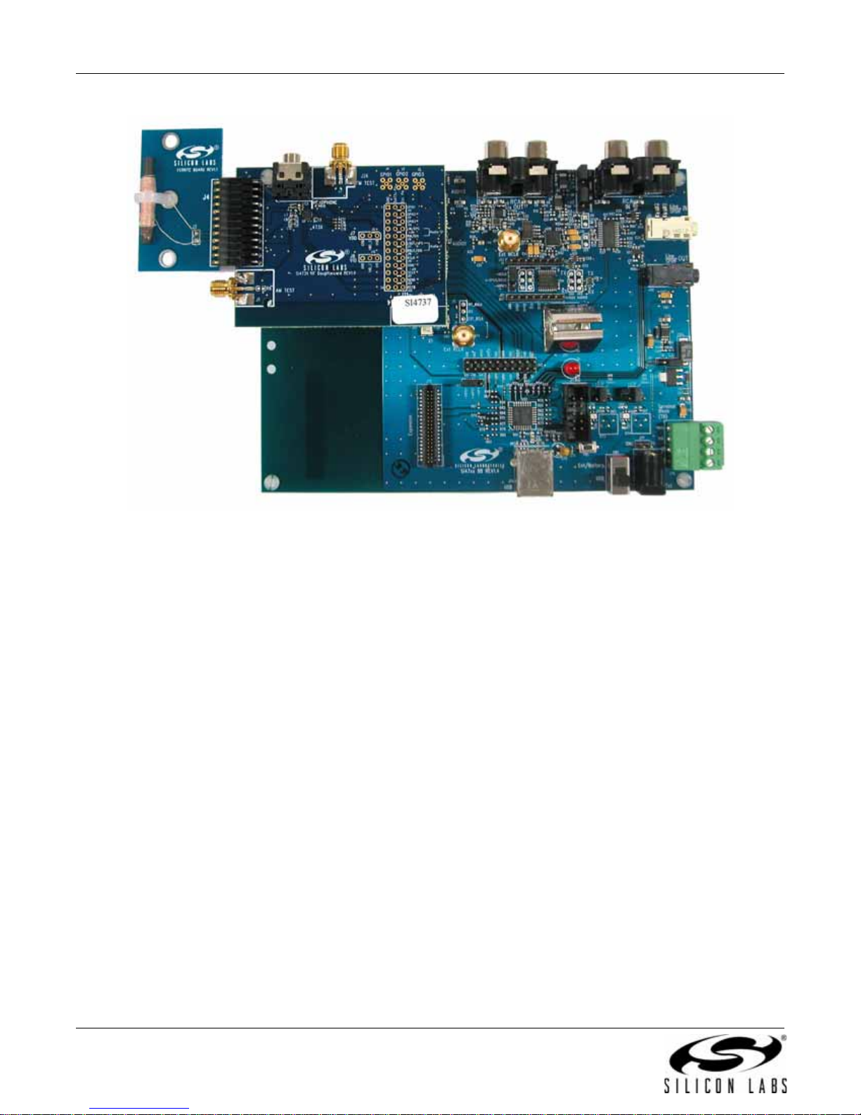
2. Description
Si47xx EVB consists of a baseboard, a daughtercard with the Si47xx part pre-mounted, and, if applicable, an
antenna card. The baseboard is common and shared among all Si47xx EVBs. The following sections refer to both
the images in the figures and the silkscreen on the Si47xx EVB. Please refer to both when using this guide.
2.1. Si47xx Baseboard
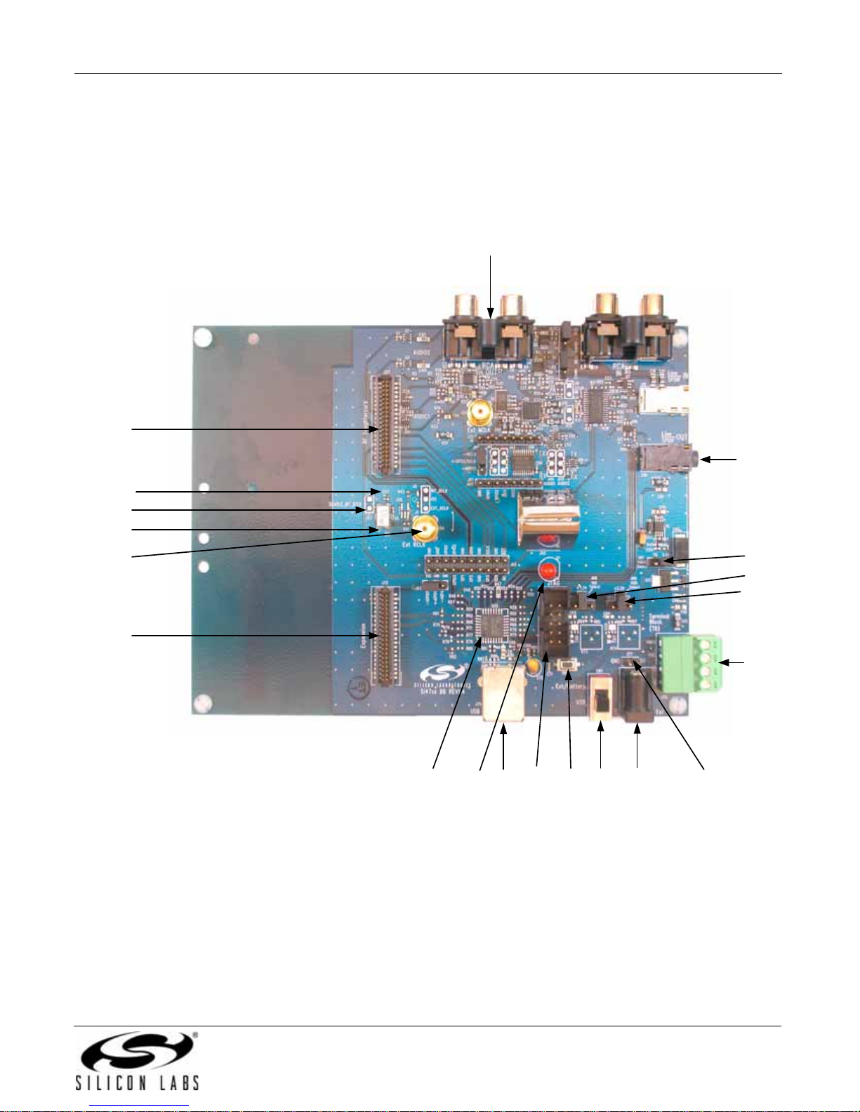
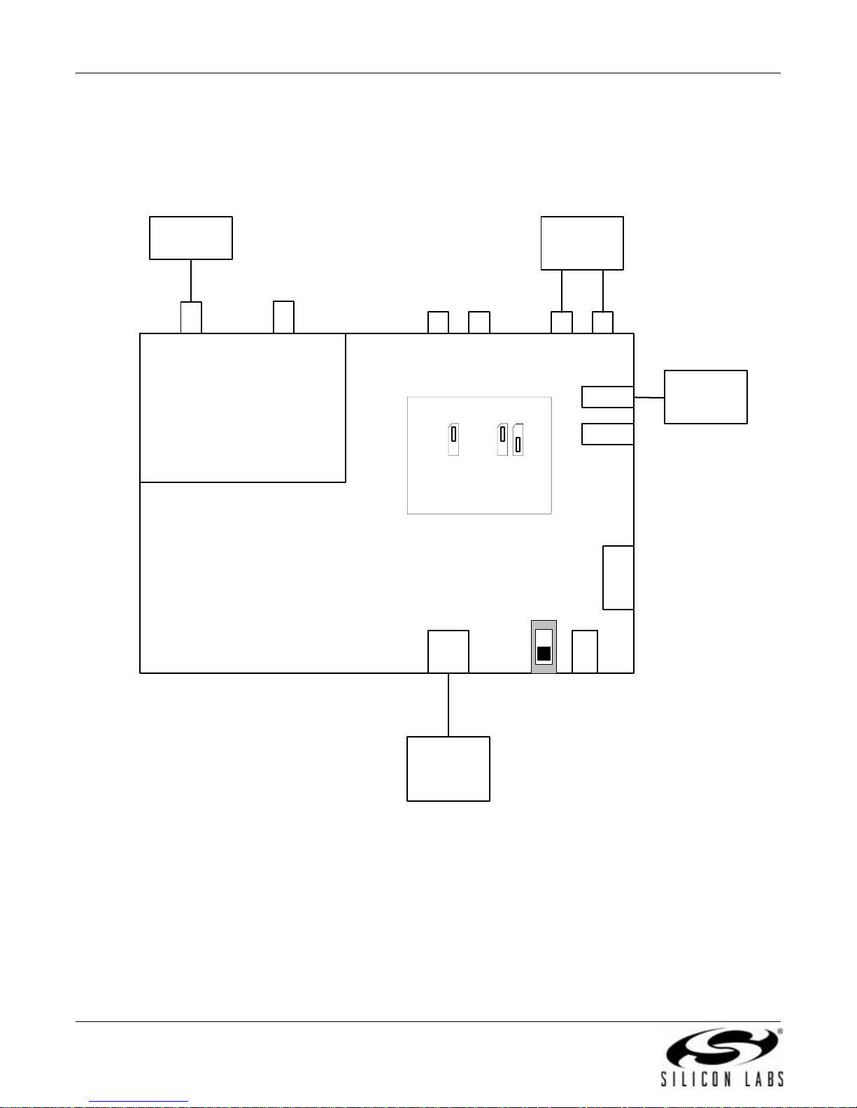
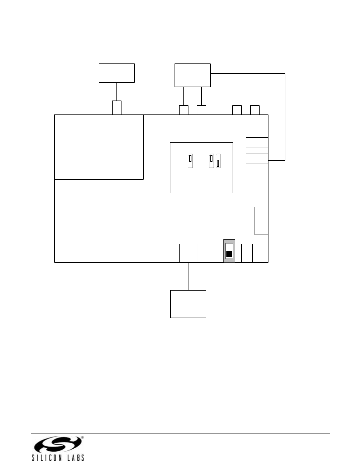
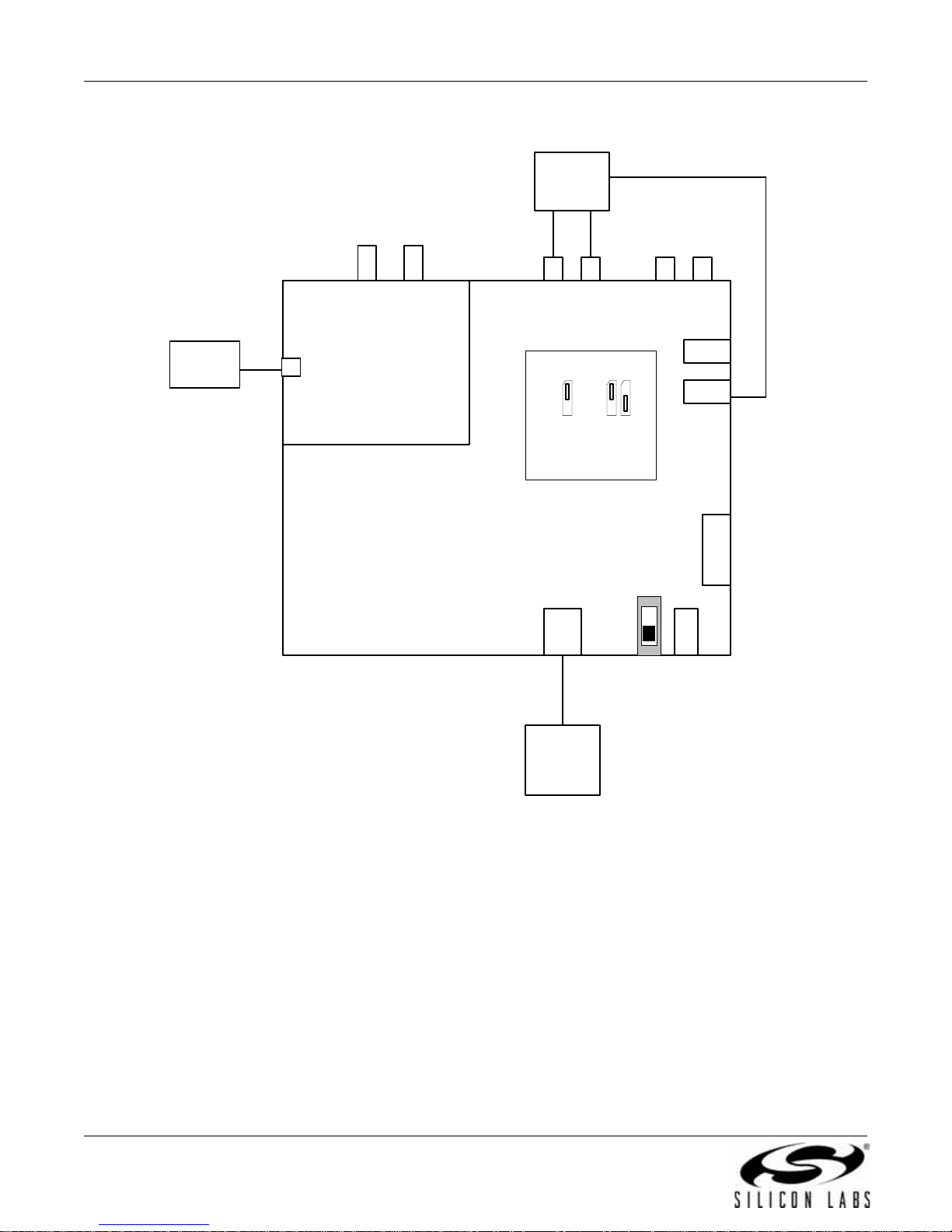
J6
J27
J30
J52
J57
X1
J54
J75
J79 SW1 J78
U22 D1
J74 PB1
Figure 1. Baseboard Connectors, Jumpers, and Devices
Baseboard power connectors/devices:
J79 USB connector (using USB power)
J78 External power connector
J77 Battery connector
J76 Terminal block (TB) power connector
SW1 Switch to select between USB power or Ext power
J61 Jumper: Baseboard power select (3.3 V or TB)
J68 Jumper: Si47xx VIO power select (3.3 V or adjustable voltage via R73 or TB)
J69 Jumper: Si47xx VDD power select (3.3 V or adjustable voltage via R74 or TB)
J61
J68
J69
J76
J77
Rev. 0.4 7
Page 8

Si47xx-EVB
Baseboard audio I/O connectors:
J6 RCA output
J30 Line output
Baseboard clock connectors/devices:
X1 32.768 kHz crystal oscillator
J52 Solder bump: select internal RCLK from oscillator
J54 Ext RCLK SMA connector input
J57 Jumper: Enable or Disable Int RCLK
Baseboard MCU connectors/devices:
U22 C8051F342 MCU
J79 USB connector to communicate with the MCU
J74 JTAG connector for the MCU
PB1 Push button to reset the MCU
D1 LED to confirm power supply to the MCU
Baseboard to daughterboard connectors:
J27 Si47xx daughtercard connector
J75 Expansion card connector (reserved)
2.1.1. Power Supply Network
J79
USB
J78
EXT
J77
BATT
SW1
1.25–3.9 V
LDO
+3.3 V
(U17)
LDO
(R73)
LDO
1.25–7 V
(R74)
Jumper
J69
Jumper
ADJ
Jumper
J68
+3.3 V
TB
Gnd
Terminal
Block (TB)
J61
ADJ
Vdd
J76
+3.3 V
TB
Vio
Vmcu
+3.3 V
Vm
TB
VIO
VDD
Daughterboard
Si47xx
11
10
VIO
VDD
8 Rev. 0.4
Figure 2. Power Supply Block Diagram
Page 9
Si47xx-EVB
The Si47xx EVB can be powered using one of the following power supply options:
1. USB power supply via J79
2. External dc (Ext DC) power supply via power jack J78 or battery via J77
3. Three separate power supplies (Vdd, Vio, Vmcu) via terminal block J76
The EVB has three supply rails: Vdd, Vio, and Vmcu. Vdd and Vio are routed directly to the daughterboard to
power the Vdd and Vio pins on the Si47xx chip, while Vmcu is used to power the baseboard.
The external dc power supply and battery should not be connected simultaneously. Refer to Section 9. "Using the
EVB with a 9 V Battery‚" on page 77 for more information.
USB Power Supply & EXT DC Power Supply
Switch SW1 is used to select between the USB power supply and Ext dc power supply.
The USB power supply or the Ext dc power supply can be configured in one of the following two modes:
1. Fixed +3.3 V
2. Adjustable Vdd and Vio
Fixed +3.3V
Only one LDO is used in this mode which outputs a +3.3 V supply to all three rails (Vdd, Vio, and Vmcu). The
jumpers need to be set according to Figure 3 to use the EVB in this configuration. This is the default configuration
on the EVB.
Vio Vdd Vmcu
ADJ
+3.3V
TB
ADJ
J69J68
+3.3V
TB
TB
J61
+3.3V
Figure 3. Default Fixed +3.3 V Jumpers Setting
Terminal Block Power Supply
If the terminal block supplies are used, then jumpers J61, J68, and J69 need to be set according to Figure 4. The
user then needs to connect three different power supp lies for Vdd, Vio, and Vmcu.
Vio Vdd Vmcu
+3.3V
ADJ
TB
J68 J61
ADJ
J69
+3.3V
TB
TB
+3.3V
Figure 4. Terminal Block Jumpers Setting
Rev. 0.4 9
Page 10
Si47xx-EVB
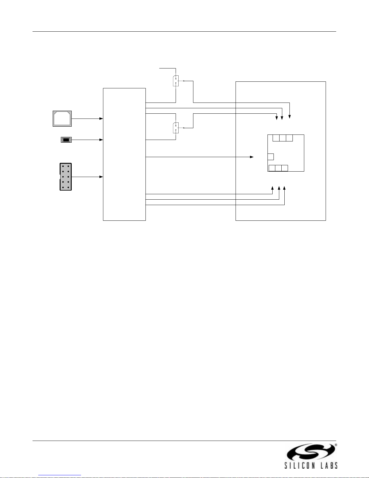
2.1.2. Microcontroller
TC_BCLK
(reserved for digital Rx )
Jumper
J41
Daughterboard
S_GPO3/DCLK
SD_GPO1
RST~
GPO1
19 18 17
Si47xx
5
6 7 8
SEN~
SCLK
GPO3/
GPO2
SDIO
DCLK
PB1
Reset
J79
USB
JTAG
J74
MCU
C8051F342
MD_GPIO3
MS_GPIO2
MD_GPIO1
Jumper
J65
MD_GP4
MS_RSTB
MS_SENB
MS_SCLK
MS_SDIO
Figure 5. MCU Block Diagram
The Si47xx EVB uses a Silicon Laboratories' C8051F342 microcontroller to control the Si47xx and to provide USB
connectivity from the host PC (via connector J79). The LED D1 illuminates to confirm that power is being properly
supplied to the C8051F342 and firmware has loaded. Push-button PB1 manually reset s the C8051F342. Th e JTAG
connector J74 is used to program the C8051F342 at production time, and is not required thereafter.
10 Rev. 0.4
Page 11

Si47xx-EVB
2.1.3. Reference Clock
Daughterboard
Jumper
J57
DIS_INT_RCLK
The Si47xx accepts a 32.768 kHz reference clock at the RCLK pin. On the EVB, this clock is provided by a
precision crystal oscillator. The user has the option of not using the onboard oscillator and bringing in the reference
clock from an external source through SMA connector J54.
When the user chooses to provide an external RCLK, jumper J52 has to be set accordingly. The user has the
option to turn off the onboard crystal oscillator by installing jumper J57.
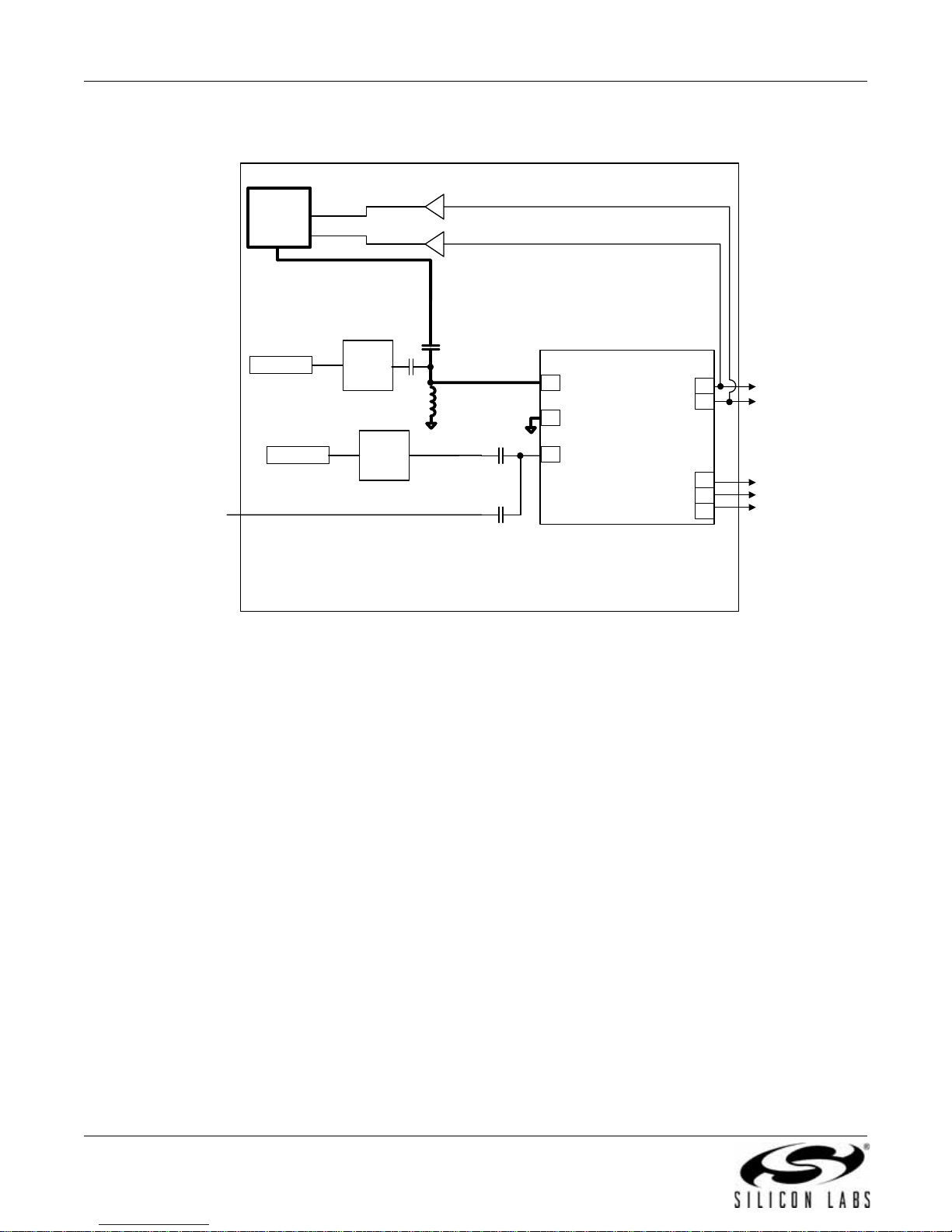
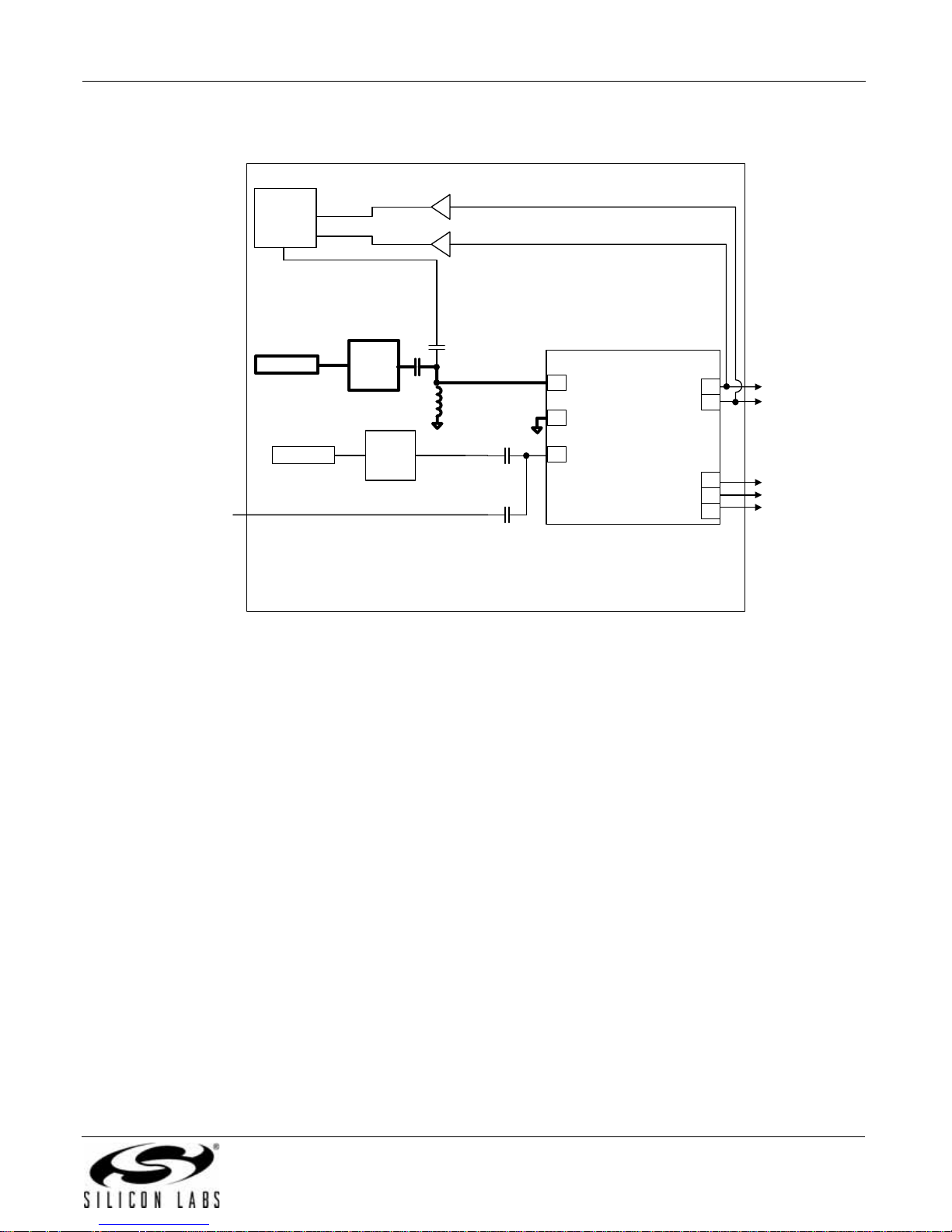
2.1.4. Audio I/O
X1
32.768 kHz
INT RClk
Jumper
INT_RCLK
J52
EXT_RCLK
J54
EXT
RClk
Figure 6. Reference Clock Block Diagram
Si47xx
9
RCLK
EVB In (TX only) 47xx Audio2 47xx Audio1 EVB Out (RX only)
TX: Analog/Digital In TX: Analog In TX: Digital In RX: Analog/Digital Out
J7
RCA In
J19
Line In
(white)
J19
SPDIF In
(white)
Jumper
J5&J13
CODEC IN
LINE
IN
S/PDIF IN
SPDIF
IN
DOUT
DOUT
0
1
Digital Input
Select
To_TX
RX: Digital Out RX: Analog Out
Audio2
Select
1
0
AUDIO2
16
LIN/ DFS2
15
RIN/ DOUT
AUDIO1
LOUT/ DFS1
ROUT/ DIN
14
13
Si47xx
Jumper
J45
AUDIO2
From_RX
(Daughterboard)
To_TX
0
1
AUDIO1
Jumper
J44
Audio1
Select
From_RX
CODEC OUT
LINE
DIN
OUT
S/PDIF OUT
SPDIF
DIN
OUT
RCA Out
0
1
Line Out
(black)
SPDIF Out
(black)
Note: Jumper J44 and J45 are automatically configured in EVB Rev 1.3.
Figure 7. Audio I/O Block Diagram
J6
J30
J30
Rev. 0.4 11
Page 12

Si47xx-EVB
The EVB supports three different kinds of configurations for the FM transmitter:
Analog In to Analog In
Analog In to Digital In
Digital In to Digital In
Analog In to Analog In: This configuration provides a way for the user to evaluate the analog audio input for FM
transmission.
The input to the EVB is an analog audio provided via the RCA input connector J7 or LINE In connector J19 (white).
Jumpers J5 and J13 are set to RCA input by default. The user has to change this jumper accordingly if LINE In is
being used. Then the analog audio inpu t is routed directly through a switch to the Si47xx Rin/Lin inputs pin 15 and
16 (Audio2).
Analog In to Digital In: This configuration provides a way for the user to evaluate the Si4 7xx digit al audio input for
FM transmission using an analog audio input.
The input to the EVB is an analog audio provided via the RCA input connector J7 or LINE In connector J19 (white).
Jumpers J5 and J13 are set to RCA input by default. The user has to change this jumper accordingly if LINE In is
being used. Then the analog audio input is converted by CODEC U10 to a serial audio digital data before it is
routed to the Si47xx digital audio input DIO and DFS pin 13 and 14 (Audio1). The DCLK input is routed to the
GPO3/DCLK pin 17. Make sure that jumper J41 is set to DCLK to ensure proper operation.
Digital In to Digital In: This configuration provides a way for the user to evaluate the Si47xx digital audio input for
FM transmission using S/PDIF digital audio commonly found in sound cards.
The input to the EVB is a digital S/PDIF data provided via the S/PDIF In connector J19 (white). The digital S/PDIF
input is converted by S/PDIF Translator U9 to a serial audio digital data before it is routed to the Si47xx digital
audio input DIO and DFS pin 13 and 14 (Audio1). The DCLK input is routed to the GPO3/DCLK pin 17. Make sure
that jumper J41 is set to DCLK to ensure proper operation.
The EVB supports analog and digital mode for receiver operation:
Analog Out to Analog Out: This configuration provides a way for the user to evaluate the analog audio output for
receiver operation. The output of the Si47xx is routed to RCA output connector J6 and Line output connector J30.
Digital Out to Digital and Analog Out: This configuration provides a way for the user to evaluate the digital audio
output for FM and AM receive using either S/PDIF digital audio or analog audio through the onboard CODEC. The
Si47xx digital audio out is routed through the S/PDIF translator µ9 to S/PDIF output connector J30 and routed
through the CODEC to RCA output connector J6 and line output connector J30.
Digital and Analog Out: This configuration provides a way for the user to evalua te the analog audio out an d digital
audio using S/PDIF digital audio for FM and AM. The analog output of the Si47xx is routed to RCA output
connector J6 and line output connector J30 and the digital audio out is routed through the S/PDIF translator to S/
PDIF output connector J30.
12 Rev. 0.4
Page 13

Si47xx-EVB
IMPORTANT: Jumper Settings
Because of the many possibilities available to configure the EVB, ensure that these four jumpers are set
accordingly:
1. J41: GPO3/DCLK setting
2. J44: TX/RX setting for Audio1 I/O (automatically set by the GUI for baseboard 1.3 and later)
3. J45: TX/RX setting for Audio2 I/O (automatically set by the GUI for baseboard 1.3 and later)
4. J5, J13: Analog Audio Source, RCA or Line In
J41: GPO3/DCLK Setting
Upper—DCLK digital audio clock
Lower—GPO3 digital control signal
For configuring the Si47xx digital audio input, make sure that the jumper is set in the Upper position so that the
DCLK signal will be routed to the Si47xx.
J44: TX/RX Setting for Audio1 I/O (automatically set by the GUI for baseboard 1.3 and later)
Upper—Audio1 is set to FM transmit (pin 13 and 14 will be the digital audio input).
Lower—Audio1 is set for FM receive (pin 13 and 14 will be analog/digital audio output).
J45: TX/RX Setting for Audio2 I/O (automatically set by the GUI for baseboard 1.3 and later)
Upper—Audio2 is set to FM transmit (pin 15 and 16 will be the analog/digital audio input).
Lower—Audio2 is set for FM receive (pin 15 and 16 will be the digital audio output).
J5, J13: Analog Audio Source, RCA or Line In
Upper—RCA inputs are used for analog audio source.
Lower—Line inputs are used for analog audio source.
Rev. 0.4 13
Page 14
Si47xx-EVB
2.2. Si47xx Daughtercards
2.2.1. Si471x/2x Daughtercard
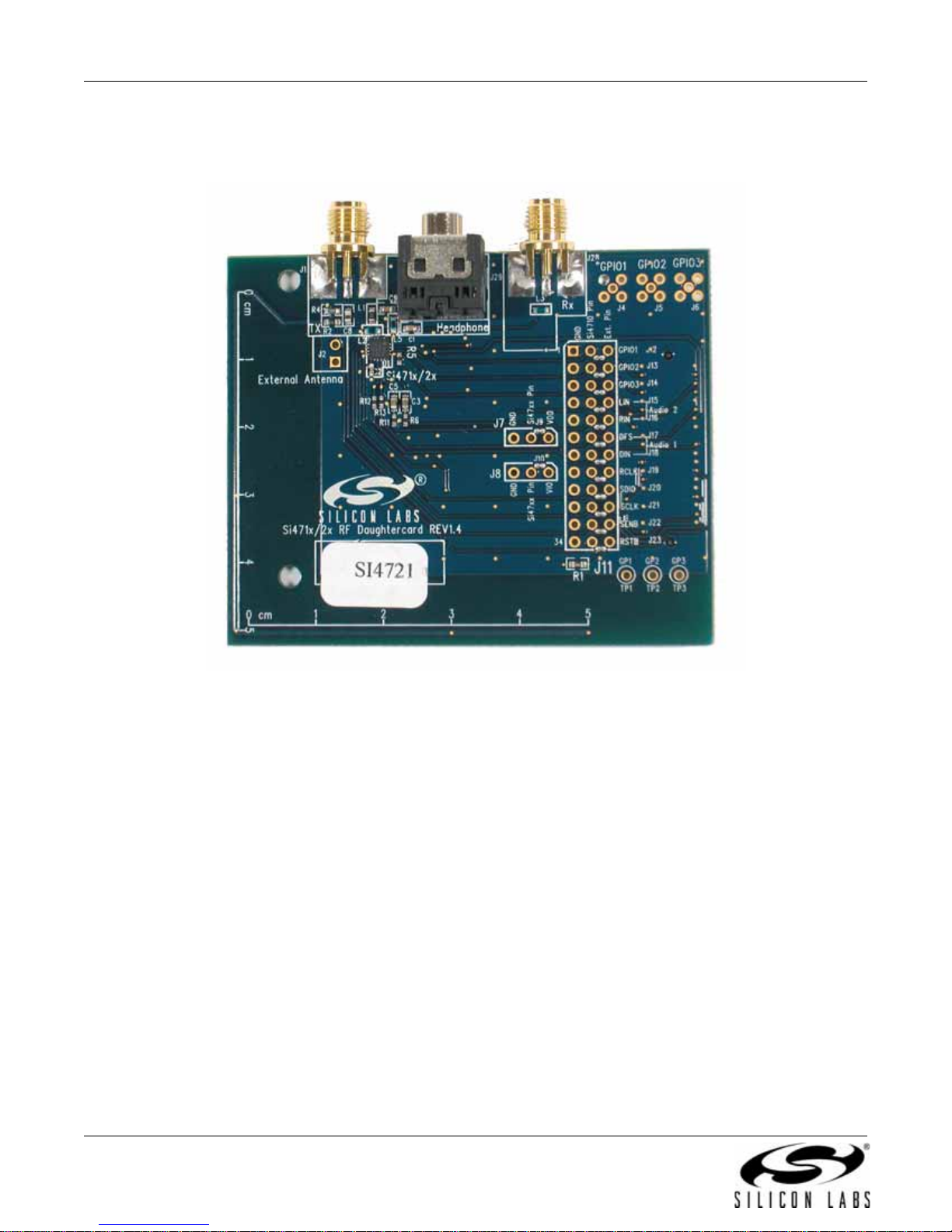
Figure 8. Si471x/2x Daughterboard Connectors and Devices
Daughterboard Connectors and Components:
U1 Si472x FM Transceiver or Si470x FM Receiver or Si471x FM Transmitter
L2 Tuning Inductor
R2 0 Ω resistor to connect FM TX output to 10 cm trace built-in antenna
C8 2 pF capacitor to connect FM TX output to J1 SMA connector
R4 50 Ω termination resistor
J1 SMA connector for FM transmitter output
J2 Header for putting external antenna for FM transmitter
J28 SMA connector for FM receiver input
J29 Headphone jack for FM receiver
14 Rev. 0.4
Page 15
Si47xx-EVB
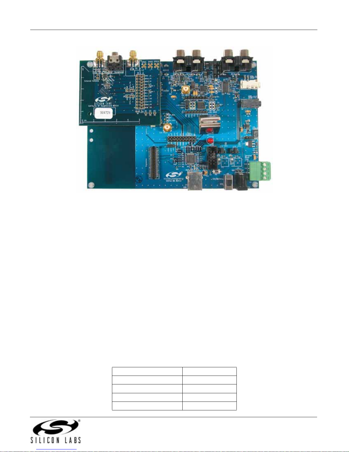
Figure 9. Fully Assembled Si471x/2x EVB
Si470x/1x/2x EVBs use Si471x/2x daughtercard with different population options depending on the individual
Si470x/1x/2x part. Please refer to individual Bill of Materials for each board.
2.2.1.1. FM Transmitter
The Si471x/2x (U1) and its bypass capacitors and tuning inductor (L2) are located on the daughtercard. The FM
transmit output can be configured in three different ways:
Built-in antenna
External antenna
RF output
Built-In Antenna
The built-in PCB trace antenna is pre-configured as the default antenna.
External Antenna
To use an external antenna, remove resistor R2. Put the external antenna in the J2 header connector.
RF Output
The FM RF output will be available through the SMA connector J1.
Refer to “AN383: Antenna Selection and Universal Layout Guidelines” for a more complete study of the antenna
interface for the Si471x/2x as an FM transmitter.
Table 3 provides the attenuation factors across the FM band when measuring the output at J1 with a 50 Ω load.
Table 3. FM Band Attenuation Factors
Frequency (MHz) Attenuation (dB)
76 32.13
88 30.91
98 30.00
108 29.20
Rev. 0.4 15
Page 16
Si47xx-EVB
2.2.1.2. FM Receiver
As an FM receiver, the FM input can be configured in three ways:
Built-in antenna
Headphone antenna
RF input
Built-In Antenna
The built-in PCB trace antenna is available by default.
Headphone Antenna
To use a headphone antenna, connect the headphone to the headphone jack J29 that is on the daughtercard. The
daughtercard also includes a headphone amplifier, which enables the user to listen to the audio output via the
headphone connected to J2 9.
RF Input
To evaluat e t he per form ance of the Si4 70x /2x as an F M receiver, connect the FM generator to the SMA connector
J28. The RF input is connected in parallel with the headphone antenna. To disconnect the RF input to eliminate
possible sources of interference, remove C9.
2.2.2. Si473x Daughtercard
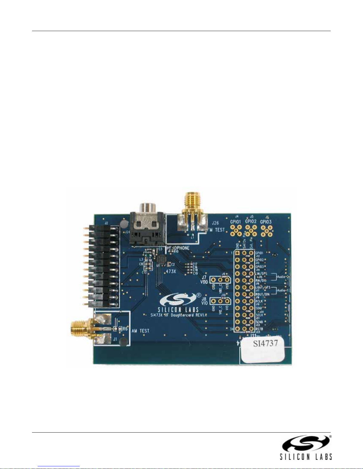
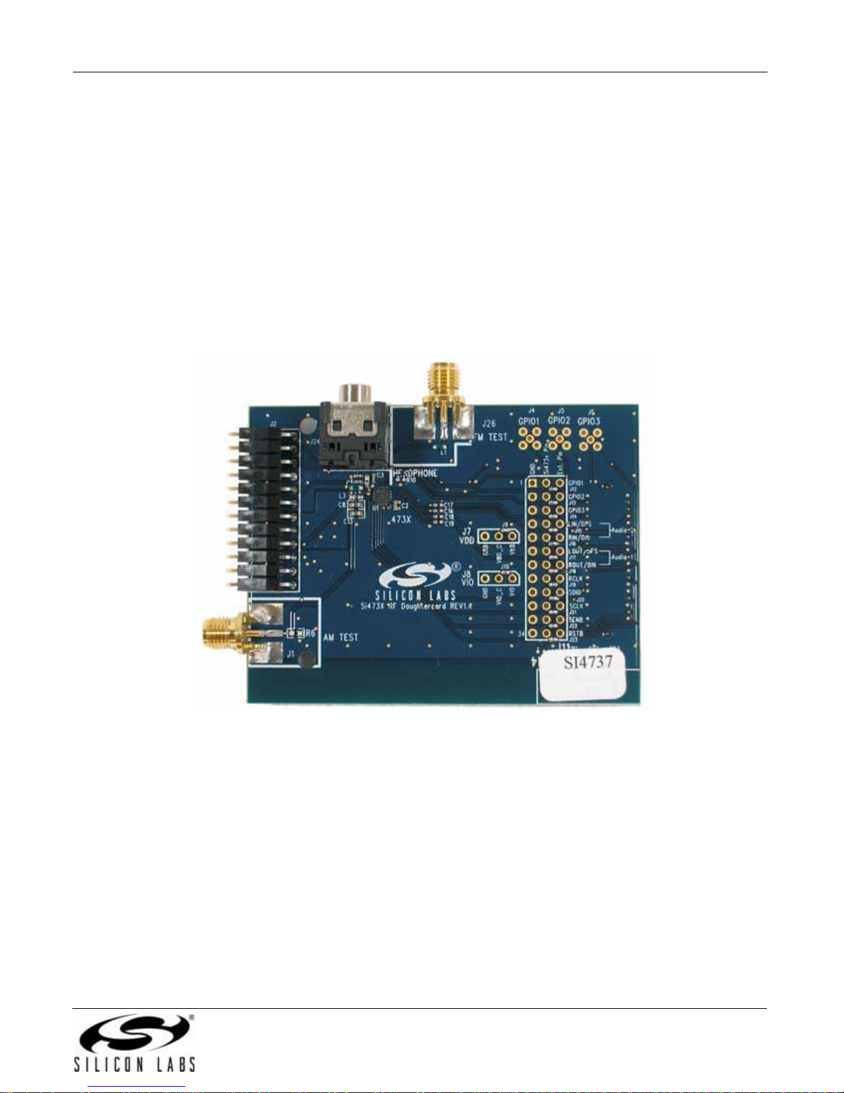
Figure 10. Si473x Daughterboard Connectors and Devices
16 Rev. 0.4
Page 17
Daughterboard connectors and components:
J1 SMA connector for AM test circuit
J2 Header for antenna interface connection
J24 Headphone jack
J26 SMA connector for FM test circuit
L4 270 nH inductor for FM input
U1 Si473x AM/FM/SW Weather Band Receiver chip
C2 Vdd bypass capacitor
C3 FM test circuit ac coupling capacitor
C8 AM input ac coupling capacitor
C12 FM input ac coupling capacitor
C13 AM test circuit ac coupling capacitor
Si47xx-EVB
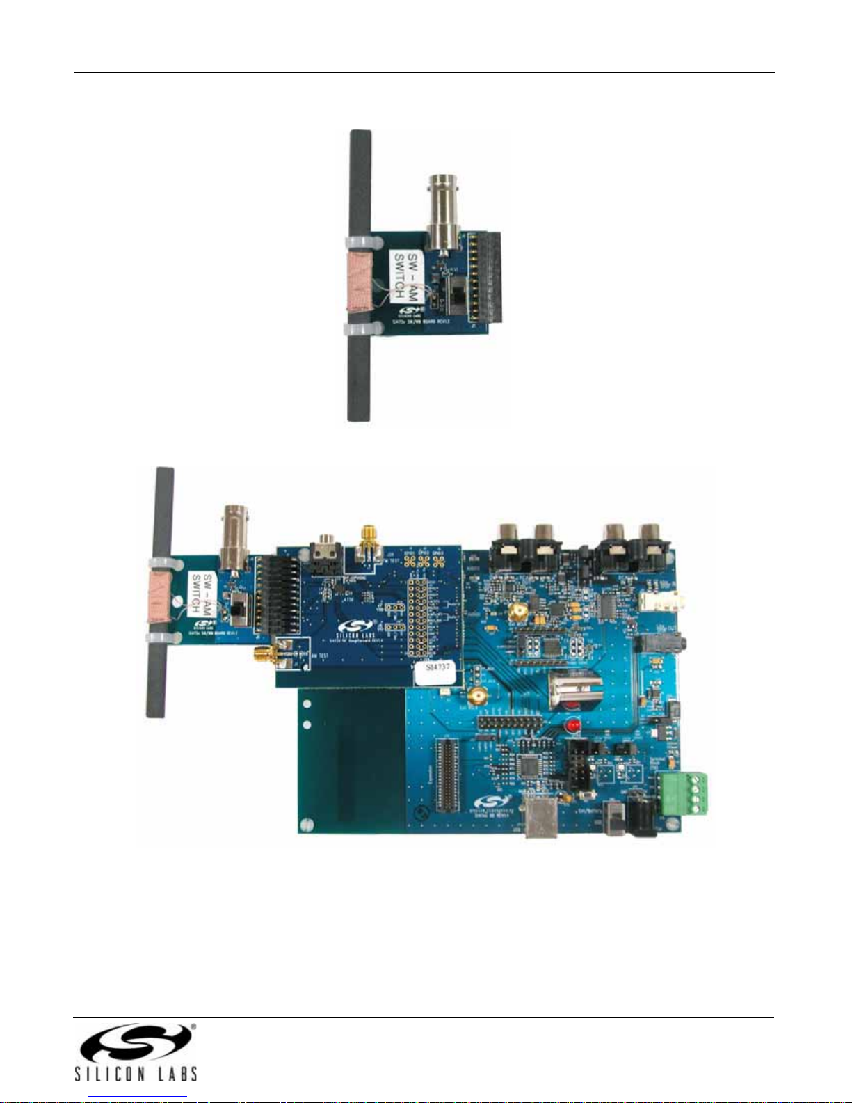
Figure 11. Fully Assembled Si473x-EVB (no antenna cards)
Rev. 0.4 17
Page 18
Si47xx-EVB
Figure 12. Fully Assembled Si473x-EVB with Ferrite Antenna Card
The daughtercard implements the Si473x AM/FM receive solution. The AM interface allows the user the option to
choose between a ferrite loop stick antenna and an airloop antenna. The user can also configure the
daughterboard to use the AM test circuit for Si473x AM character ization. Th e FM interface allows th e user to att ach
a headphone for the antenna interface or use the FM test circuit input for Si473x FM characterization. Individual
SW and weather band antenna cards provide the option of using a whip antenna for reception.
2.2.3. Si473x AM/FM/SW Weather Band Receiver Chip
The Si473x (U1) along with its bypass capacitor is located on the daughterboard. The front-end circuit of the
daughterboard includes antenna interfaces and test circuits for AM and FM reception followed by ac coupling
capacitors going into the AM and FM inputs of the Si473x.
18 Rev. 0.4
Page 19
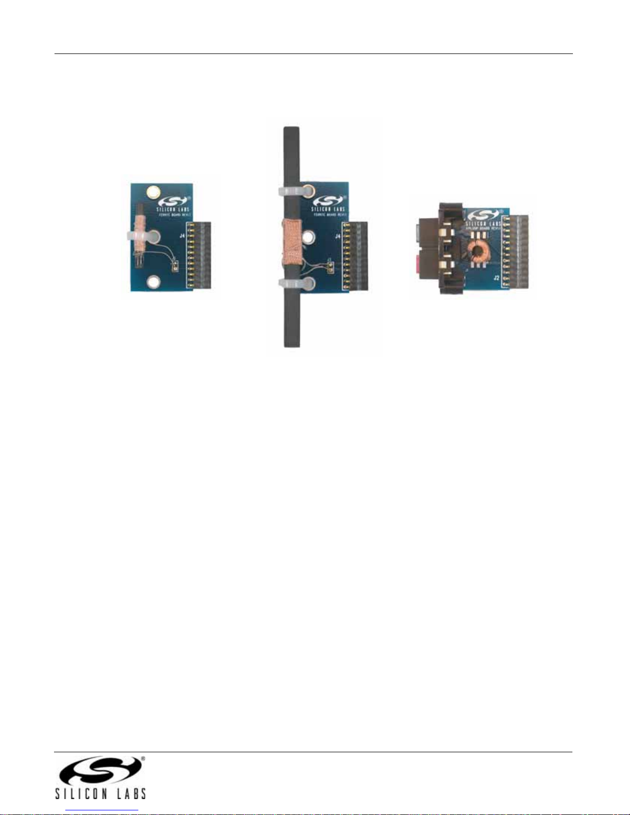
2.2.4. Antenna Interfaces
2.2.4.1. AM Antenna Interface
Si47xx-EVB
Figure 13. Antenna Board Options—SL4X30MW100T Ferrite, SL5X7X100MW70T Ferrite, and
SL9X5X4MWTF Airloop
The user has the flexibility of choosing one of the two available antenna options. The user can either decide to use
the airloop antenna or the ferrite loop stick antenna.
Rev. 0.4 19
Page 20
Si47xx-EVB
2.2.4.1.1. Ferrite Loop Stick Antenna
A ferrite loop stick antenna can be used with the Si473x by connecting the ferrite antenna board as shown in
Figure 14.
J24
Head
Phone
Jack/FM
Antenna
FM Input
Buffers
C12
C3
L4
C13
C8
Daughterboard
2
FM Input
3
RFGND
4
AM Input
Analog
Audio Out
LOUT
ROUT
Si473x
Digital*
Audio Out
GPO3/DCLK
DFS
DOUT
U1
*Note: Si4731/5/7/9 only
with FW 2.0 or higher
14
13
17
16
15
Ferrite Loop
Stick Antenna
Board
J2
J26
SMA IN
SMA IN
FM
Test
Circuit
J1
AM
Test
Circuit
Figure 14. Ferrite Loop Stick Antenna Interface for AM Reception on the Si473x Daughterboard
The Si473x accepts a wide range of ferrite loop sticks from 180 to 600 µH with no manual alignment necessary. To
test a specific ferrite loop stick, install the individual ferrite antenna board.
20 Rev. 0.4
Page 21
Si47xx-EVB
2.2.4.1.2. Airloop Antenna
An airloop antenna can be used by connecting the airloop antenna board as shown in Figure 15.
J24
Head
Phone
Jack/FM
Antenna
FM Input
Buffers
C12
C3
L4
C13
C8
Daughterboard
2
FM Input
3
RFGND
4
AM Input
Analog
Audio Out
LOUT
ROUT
Si473x
Digital*
Audio Out
GPO3/DCLK
DFS
DOUT
U1
*Note: Si4731/5/7/9 only
with FW 2.0 or higher
14
13
17
16
15
Airloop
Antenna
Airloop Antenna
Board
J2
J26
SMA IN
SMA IN
FM
Test
Circuit
J1
AM
Test
Circuit
Figure 15. Airloop Antenna Interface for AM Reception on the Si473x Daughterboard
The airloop antenna board has a transformer, U1. The purpose of the transformer is to gain up the inductance from
the airloop for proper operation. Using a 1:5 turn ratio inductor, the inductance is increased by 25 times and easily
supports all typical AM airloop antennas, which generally vary between 10 and 20 µH.
Rev. 0.4 21
Page 22
Si47xx-EVB
2.2.4.2. FM Antenna Interface
J24
Head
Phone
Jack/FM
Antenna
Buffers
FM Input
C12
C3
L4
C13
C8
Daughterboard
2
FM Input
3
RFGND
4
AM Input
Analog
Audio Out
LOUT
ROUT
Si473x
Digital*
Audio Out
GPO3/DCLK
DFS
DOUT
U1
*Note: Si4731/5/7/9 only
with FW 2.0 or higher
14
13
17
16
15
J2
J26
SMA IN
SMA IN
FM
Test
Circuit
J1
AM
Test
Circuit
Figure 16. Headphone Antenna Interface for FM Rece ption on the Si473x Daughterboard
The FM input on the Si473x is a single-ended input and uses the headphone jack with headphones connected to
provide an antenna for FM reception. Please refer to "A N3 83 : Ante nn a Sele ction a nd Un iversa l Layo ut Gu ide lines"
for more information.
22 Rev. 0.4
Page 23
2.2.4.3. SW and Weather Band Antenna Interface
Figure 17. SW/WB Antenna Card (SW population option shown)
Si47xx-EVB
Figure 18. Fully Assembled Si473x-EVB with SW/WB Antenna Card
The BNC connector, J2, will be used to connect a whip antenna for shortwave, FM, and weather band reception.
For SW reception, switch S1 must be in the SW position . The ferrite bar is used for AM reception, and the switch
S1 must be in the AM position for AM reception.
When using the WB Antenna Card, WB reception is through the whip antenna. For a better listening experience,
plug the headphones to J30 rather than J24.
Note: LW no t supported with SW/WB Antenna Card.
Rev. 0.4 23
Page 24

Si47xx-EVB
2.2.5. Test Circuit Interfaces
2.2.5.1. AM/LW/SW Test Circuit Interface
J24
Head
Phone
Jack/FM
Antenna
FM Input
Buffers
C12
C3
L4
C13
C8
Daughterboard
2
FM Input
3
RFGND
4
AM Input
Analog
Audio Out
LOUT
ROUT
Si473x
Digital*
Audio Out
GPO3/DCLK
DFS
DOUT
U1
*Note: Si4731/5/7/9 only
with FW 2.0 or higher
14
13
17
16
15
J2
J26
SMA IN
SMA IN
FM
Test
Circuit
J1
AM
Test
Circuit
Figure 19. Test Circuit Interface for the Si473x Daughterboard
The antenna cards must be disconnected during AM test ing with J1. For best sensitivity measurem ents, disconnect
C8 to eliminate possible noise sources.
24 Rev. 0.4
Page 25
2.2.5.2. FM/Weather Band Test Circuit Interface
J24
Head
Phone
Jack/FM
Antenna
FM Input
Si47xx-EVB
Buffers
C12
C3
L4
C13
C8
Daughterboard
2
FM Input
3
RFGND
4
AM Input
Analog
Audio Out
LOUT
ROUT
Si473x
Digital*
Audio Out
GPO3/DCLK
DFS
DOUT
U1
*Note: Si4731 only with
FW 2.0 or higher
14
13
17
16
15
J2
J26
SMA IN
SMA IN
FM
Test
Circuit
J1
AM
Test
Circuit
Figure 20. FM Test Circuit on the Si473x Daughterboard
The user does not need to do anything to setup the FM test circuit other than to make sure that the headphone is
disconnected. The test circuit is connected in parallel with the headphone antenna. To eliminate possible sources
of interference, remove C12.
Rev. 0.4 25
Page 26
Si47xx-EVB
3. Recommended Hardware Setup
The Si47xx-EVB can be configured for FM transmit, FM receive, weather band receiver, or AM/SW receive. The
following is a description of how to correctly configure the device for either mode of operation.
3.1. Hardware Setup for FM Transmitter Test
Analyzer
SMA Cable
FM OUT RCA IN
RF
J1
Si471x/2x
Daughterboard
Si47xx
Baseboard
FM IN
J28
J6
RCA OUT
Jumpers
Setting
DCLK
GPIO3
Note: J44 and J45 are
automatically configured in
EVB Rev1.3 and later
J41
TX
RX
J44 J45
USB
EXT pwr
Generator
TX
RX
SW1
Analog
Audio
RCA Cable
J7
J19
J30
J76
S/PDIF
Audio
Generator
Terminal
Block (TB)
J79
USB pwr
J78
EXT Jack
USB Cable
PC
w/ USB
port
Figure 21. Hardware Setup for FM Transmitter Test
1. Connect the USB cable from PC to the EVB USB connector J79. The USB connection will serve as a dual purpose:
supplying the power to the EVB and controlling the EVB.
2. Connect an analog audio generator to the RCA input connector J7 using an RCA cable or connect an SPDIF digital audio
generator to connector J19 using an SPDIF cable.
3. Connect an RF analyzer from the FM output SMA connector J1 using an SMA cable.
26 Rev. 0.4
Page 27
3.2. Hardware Setup for FM or Weather Band Receiver Test
Si47xx-EVB
RF
Generator
SMA Cable
FM IN
Si47xx
Daughterboard
Si47xx
Baseboard
J28 or J26
RCA Cable
GPIO3
Audio
Analyzer
J6
RCA OUT
Jumpers
Setting
DCLK
Note: J44 and J45 are
automatically configured in
EVB Rev1.3 and later
J41
TX
RX
J44 J45
USB
EXT pwr
TX
RX
SW1
RCA IN
J7
Optical
Cable
J19
S/PDIF
OUT
J30
J76
Terminal
Block (TB)
J79
USB pwr
J78
EXT Jack
USB Cable
PC
w/ USB
port
Figure 22. Hardware Setup for FM/Weather Band Receiver Test
1. Connect the USB cable from PC to the EVB USB connector J79. The USB connection will serve as a dual purpose,
supplying the power to the EVB and controlling the EVB.
2. Connect an audio analyzer from the RCA output connector J6 using an RCA cable.
3. Connect an RF generator to the FM input SMA connector J28 or J26 using an SMA cable.
4. Connect an audio analyzer to the S/PDIF output connector, J30, using an optical cable.
5.
To avoid possible sources of interference, please remove C9 or C12 (depending on the daughtercard). This wi ll
disconnect the headphone circuit from the test circuit.
Rev. 0.4 27
Page 28
Si47xx-EVB
3.3. Hardware Setup for AM Receiver Test
Audio
Analyzer
RCA Cable
RF
Generator
SMA Cable
J1
Daughterboard
F M IN
J24
Si473x
Si47xx
Baseboard
J28 or J26
RCA OUT
DCLK
GPIO3
automatically configured in
J79
USB Cable
J6
Jump ers
Se ttin g
TX
RX
J44 J45
J41
Note: J44 and J45 are
EVB Rev1.3 and later
USB
EXT pwr
USB pwr
TX
RX
SW1
RCA IN
EXT Jack
J7
Optical
Cable
J19
S/PDIF
OUT
J30
J76
Terminal
Block (TB)
J78
PC
w/ USB
port
Figure 23. Hardware Setup for AM Reception
1. Connect the USB cable from PC to the EVB USB connector, J79. The USB connection will not only allow controlling of the
EVB, but will also provide power to the EVB.
2. Connect either the ferrite antenna or the airloop antenna board. The user also has the option of using the AM test input for
characterization by connecting the AM test input connector J1 to an RF generator source.
3. Connect an audio analyzer to the RCA output (connector J6) using an RCA cable for the analog audio output.
4. Connect an audio analyzer to the S/PDIF output (connector J30) using an optical cable.
5. Or, connect the headphone output to J24 on the daughtercard.
28 Rev. 0.4
Page 29
Si47xx-EVB
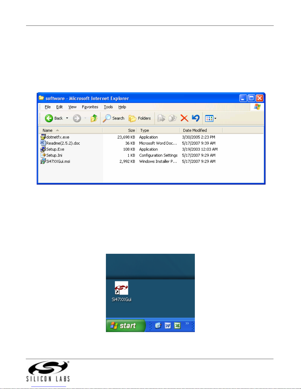
4. Getting Started—Software Installation
The Si47xx Windows GUI (graphical user interface) software is designed for use with the Si47xx evaluation board
(EVB). The GUI software revision number is available under Help
The GUI software development program uses a host machine USB port to communicate with the Si47xx EVB and
is tested for use with Windows XP and Windows 2000.
To install, insert the Silicon Laboratories Si47xx CD into the host machine CD drive and launch Windows Explorer.
Open the CD to explore the contents in a window like the one shown in Figure 24.
→About.
Figure 24. Installation and Setup Screen
Important: Open and read the Readme.doc file at this point. It may contain information that is not captured here,
and which could be very important to the functionality of the EVB or software.
Run the Setup.Exe and follow the instructions on the screen.
Note: If you get this Error message: "This setup requires the .NET Framework version 2.0," then you should install the .NET
Framework that is provided on the CD and re-run the setup. The GUI requires version 2.0; however, multiple versions
such as 1.1, 2.0, and 3.0 can be installed simultaneously.
After installation is finished, an Si47XXGui icon will appear on your desktop. Launch the software by clicking this
icon on the desktop as shown in Figure 2 5.
Figure 25. Launching the GUI
Rev. 0.4 29
Page 30
Si47xx-EVB
5. FM Transmitter GUI
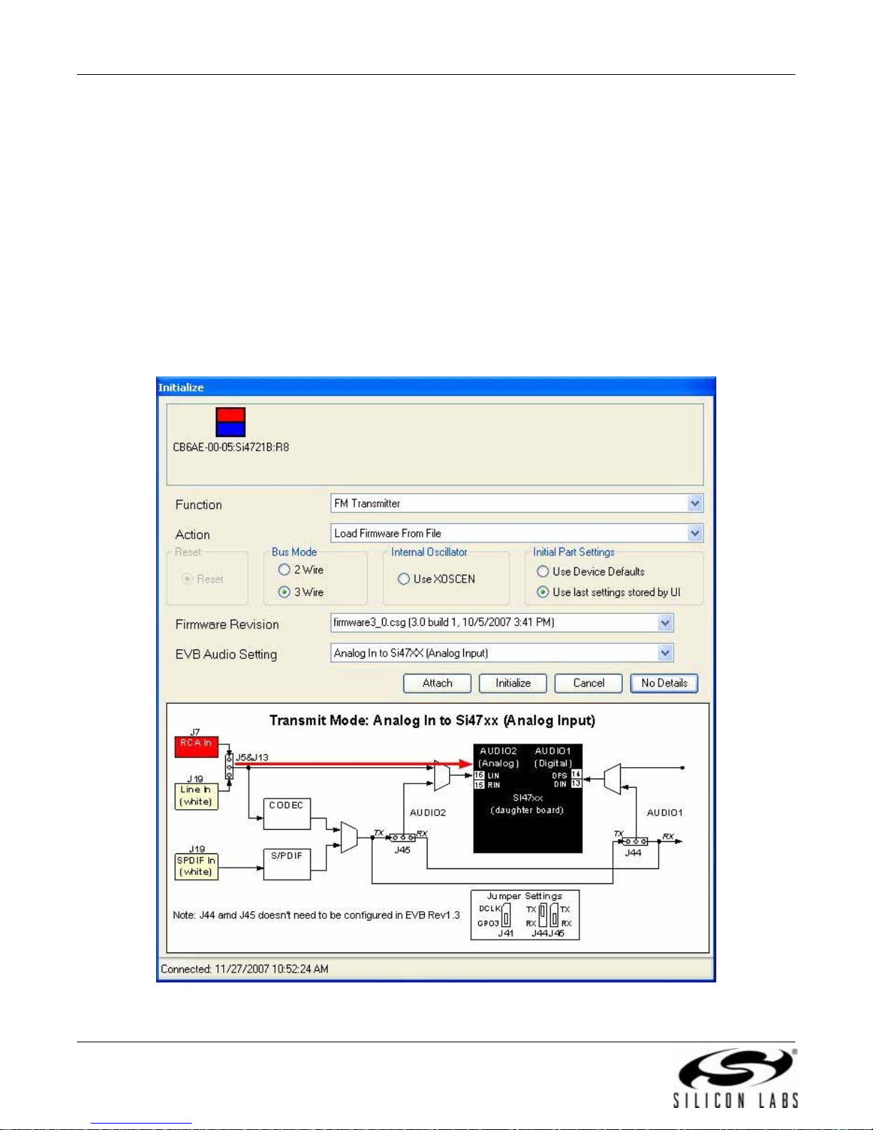
The first Si47xx window is the Initialization window as shown in Figure 26.
Select the FM transmitter function.
As an FM transmitter, there are three audio input settings available:
Analog Input
Analog to Digital Input
Digital Input
5.1. Configuring the Si47xx as an FM Transmitter Using Analog Audio Input
This mode configures the Si47xx to receive analog audio input at pin 15 and 16 (LIN and RIN). The user has the
ability to provide analog audio from RCA In connector (J7) or Line In (J19). Set jumpers J5 and J13 accordingly.
Figure 26 shows the configuration setting for analog audio input. Select the device, busmode, firmware revision,
and initial part settings and then click Initialize. A new window displaying "Initializing FM Transmitter" will appear.
Figure 26. Configuring the Si47xx to Transmit Analog Input
30 Rev. 0.4
Page 31

Si47xx-EVB
5.2. Configuring the Si47xx as an FM Transmitter Using Digital Audio with Analog Audio
Source
This mode configures the Si47xx to receive digital audio input at pin 13 and 14 (DIN and DFS), but the user still
provides an analog audio source to the EVB. It is useful for a user who wants to test digital input on the Si47xx but
does not have a digital audio source. The analog audio source is converted to digital audio through the CODEC,
which can be configured to output various digital audio formats. Refer to Figure 32, “CODEC Settings Property
Window,” on p age 39 to contr ol the CODEC. Select the device, busmode, firmware revision, and initial part settings
and then click Initialize. A new window displaying "Initializing FM Transmitter" will appear.
Notes:
Set jumper J41 according to Figure 27 to properly operate in digital mode.
1.
2. Jumpers J44 and J45 are automatically set by the GUI with baseboard revision 1.3 and later.
Figure 27. Configuring the Si47xx to Transmit Digital Input by Using Analog Source (CODEC)
Rev. 0.4 31
Page 32

Si47xx-EVB
5.3. Configuring the Si47xx as an FM Transmitter Using Digital Audio with SPDIF Digital
Source
This mode configures the Si47xx to receive digital audio input at pin 13 and 14 (DIN and DFS) when the user has
an SPDIF digital audio source. The SPDIF source is converted to PCM digital audio by the SPDIF translator. Refer
to Figure 33, “SPDIF Settings Property Window,” on page 40 to control the SPDIF translator.
Notes:
Set jumper J41, J44, and J45 according to Figure 28 to properly operate in digital mode.
1.
2. Jumpers J44 and J45 are automatically set by the GUI with baseboard revision 1.3 and later.
3. The Si47xx requires the digital audio signal to be present when initializing the part. Therefore, connect the SPDIF IN
signal prior to initializing the part.
Figure 28. Configuring the Si47xx to Transmit Digital Input by Using Digital Source (SPDIF)
TIP. If the Si47xx Development GUI doesn't find your device, try unplugging and plugging in the USB cable again.
32 Rev. 0.4
Page 33

5.4. FM Transmitter Main Window
The FM transmitter main window will appear after initialization.
Si47xx-EVB
1
2
3
7
9
10
11
12
13
14
15
16
4
25
5
17
24
6
8
18
19
20
21
22
23
Figure 29. FM Transmitter Main Window
Table 4. FM Transmitter Main Window Descriptions
# Description Range
1
Transmit frequency display. Enter the desired FM transmit frequency in this window.
2
Transmit voltag e display. Enter the desired FM transmit voltage in this window.
3
Varactor Value. This is an indicator showing the tuning cap value of the Si472x device.
Each number represents 0.25 pF. If the varactor value is manually overwritten in the
property window, the indicator will change from automatic mode to manual mode.
4
RF on or off. Turning this button on will enable the FM transmit, while turning this button
off will disable the FM transmit.
5
Pre-Emphasis. Click one of the three buttons to set the pre-emphasis e ither to Of f, 50 µs
or 75 µs.
6
Si472x EVB audio input setting indicator: Analog In/Digital (Analog In to CODEC)/Digital
(SPDIF).
7
Presets. Press and hold the desired preset button for 1.5 seconds to program. The current frequency will replace the preset number. Press for less than 1.5 seconds to tune to
the displayed frequency. Presets can also be programmed automatically from the
Receive Power Scan window.
8
Pilot Tone Generation. Set to 19 kHz and select "Pilot On" when in stereo mode. Set to
0–19 kHz for and select "Pilot On" for test tone generation.
9
Audio Deviation. Enter the desired audio deviation in this window.
10
Pilot Deviation. Enter the desired pilot deviation in this window.
76–108 MHz
88–120 dBuV
1–191
On/Off
Off, 50 µs, 75 µs
Analog, Digital
CODEC, Digital
SPDIF
76–108 MHz
0–19 kHz
0–90 kHz
0–90 kHz
Rev. 0.4 33
Page 34

Si47xx-EVB
Table 4. FM Transmitter Main Window Descriptions (Continued)
# Description Range
11
RDS Deviation. Enter the desired RDS deviation in this window (Si4721 only).
12
Total Deviation. This is an indicator only displaying the sum of the audio, pilot and RDS
deviation. If the total deviation exceeds 75 kHz, the indicator will turn red and a warning
sign is displayed.
13
Input Mute Left/Right. Turning this button will mute the Left or Right audio channel.
14
Turn on or off th e pilot tone for stereo or mono FM transmit mode.
15
Turn on or off the RDS transmission (Si4721 only).
16
Modulation On. Clicking this button on will modulate the audio, pilot, and RDS signal
according to the audio, pilot, and RDS deviation. Turning this button off will turn off modulation for all audio, pilot, and RDS signal and only the carrier will be transmitted.
17
Turn on or off th e L-R channel for stereo or mono FM transmit mode.
18
Turn on or off the compressor for the audio signal.
19
Attack time. Set the attack time for the compressor in milliseconds.
20
Release time. Set the release time for the compressor in milliseconds.
21
Threshold. Set the threshold for the compressor.
22
Input Gain. Set the compressor gain.
23
Limiter Release Time. Set the limiter release time constant.
24
Turn on or off the limiter feature.
25
Audio Level Indicators. Overmodulation, Limiter, Audio input level below low-level
threshold (silence detection), and Audio input level below high-level threshold (loud
detection). To enable these four indicators, check the Enable Interrupts box. These
indicators are sticky; to clear them, click the Reset button.
0–7.5 kHz
0–187.5 kHz
On/Off
On/Off
On/Off
On/Off
On/Off
On/Off
0.5–5 ms
100–1000 ms
–40 to 0 dBFS
0 to 20 dB
0.5,1,2,3,4,5,6,7,8,
9,10,20,30,40,50,
75,100 ms
On/Off
—
34 Rev. 0.4
Page 35

Si47xx-EVB
5.5. FM Transmitter Settings (Analog Mode) Property Window
FM transmitter settings are configu red by selecting Wind ows→Properties→FM Transmitter Settings when analog
mode is selected in the initialization window.
Table 5. FM Transmitter Settings in Analog Mode Property Window Descriptions
Item Description Range
Reference Clock
Frequency (Hz)
Reference Clock
Prescaler
Varactor Capacitor
Overwrite
Audio Level Low
Threshold (dBFS)
Audio Level Low
Duration (mSec)
Audio Level High
Threshold (dBFS)
Figure 30. FM Transmitter Settings in Analog Mode Property Window
This field is used to specify the frequency of the reference clock.
The input to the RCLK pin divided by the prescaler is the
reference clock. The reference clock must be in the range of
31130 to 34406 Hz.
This field is used to specify the prescaler value. T he inpu t to the
RCLK pin divided by the prescaler is the reference clock. The
reference clock must be in the range of 31130 to 34406 Hz.
This field allows the user to manually overwrite the tuning
capacitance. A number 0 indicates that the tuning cap is
automatically adjusted. Any number other than 0 (1 to 191) will
indicate that the tuning cap is manually adjusted.
An interrupt will be generated when the audio input level falls
below this threshold for the duration greater than the Audio
Level Low Distortion setting. This may be called silence
detection indicator.
Set the duration for the audio level low before an interrupt is
generated.
An interrupt will be generated when the audio input level rises
above this threshold for the duration greater than the Audio
Level High Duration setting. This may also be called loud
detection indicator.
31130–34406 Hz
1–4095
Automatic: 0,
Manual: 1–191
–70 to 0
0–65535
–70 to 0
Rev. 0.4 35
Page 36

Si47xx-EVB
Table 5. FM Transmitter Settings in Analog Mode Property Window Descriptions (Continued)
Item Description Range
Audio Level High
Duration (mSec)
Line Input
Attenuation
Maximum Line Input
Level
Set the duration for the audio level high before an interrupt is
generated.
The Si47xx has four attenuator settings (636, 416, 301, and
190 mVp). It will tell the maximum audio input signal that the
user can give to the LIN and RIN input. The attenuator setting
will determine the audio input impedance (LIN and RIN) of the
device.
The maximum line input level of the max audio input signal that
the user supplies to the device. This number has to be less than
or equal to the attenuation setting. The max line input level will
correspond to the max audio deviation set in the audio deviation
window on the main GUI. Make sure that the actual audio input
signal does not exceed this limit, otherwise the audio signal will
become distorted.
0–Line Input Attenuation
0–65535
190mVp, 301mVpk,
416mVp, 636mVpk
36 Rev. 0.4
Page 37

Si47xx-EVB
5.6. FM Transmitter Settings (Digital Mode) Property Window
FM transmitter settings are configured by selecting Windows→Properties→FM Transmitter Settings when
CODEC or SPDIF mode is selected in the initialization window.
Figure 31. FM Transmitter Settings in Digital Mode Property Window
Table 6. FM Transmitter Settings in Digital Mode Property Window Descriptions
Item Description Range
Reference Clock
Frequency (Hz)
Reference Clock
Prescaler
V aractor Capacitor
Overwrite
Audio Level Low
Threshold (dBFS)
Audio Level Low
Duration (mSec)
Audio Level High
Threshold (dBFS)
Audio Level High
Duration (mSec)
This field is used to specify the frequency of the reference clock. The
input to the RCLK pin divided by the prescaler is the reference clock.
The reference clock must be in the range of 31130 to 34406 Hz.
This field is used to specify the prescaler value. The input to the RCLK
pin divided by the prescaler is the reference clock. The reference
clock must be in the range of 31130 to 34406 Hz.
This field allows the user to manually overwrite the tuning
capacitance. 0 indicates that the tuning cap is automatically adjusted.
Any number other than 0 (1 to 191) will indicate that the tuning cap is
manually adjusted.
An interrupt will be generated when the audio input level falls below
this threshold for the duration greater than the Audio Level Low
Distortion setting. This may be called silence detection indicator.
Set the duration for the audio level low before an interrupt is
generated.
An interrupt will be generated when the audio input level rises above
this threshold for the duration greater than the Audio Level High
Duration setting. This may also be called loud detection indicator.
Set the duration for the audio level high before an interrupt is
generated.
31130–34406 Hz
1–4095
Automatic: 0
Manual: 1–191
–70 to 0
0–65535
–70 to 0
0–65535
Rev. 0.4 37
Page 38

Si47xx-EVB
Table 6. FM Transmitter Settings in Digital Mode Property Window Descriptions (Continued)
Item Description Range
Digital Format
Digital Sample
Precision
Digital Sample
Rate (Hz)
Digital Mono
Mode Enable
Digital DCLK
Falling Edge
2
Sets I
S of left justified digital format.
Select the precision of the digital audio input.
Sets the DFS digital sample rate. Must be set to 0 Hz befo re DCLK/
DFS is removed.
Select between Digital Stereo or Mono.
Select between using rising edge or falling edge of DCLK when
sampling Digital Input (DIN) data.
Left-Justified, I
DSP (MSB on first
DCLK), or DSP (MSB
on second DCLK)
8, 16, 20, 24 bits
0, 32000–48000 Hz
On/Off
On/Off
2
S,
38 Rev. 0.4
Page 39

Si47xx-EVB
5.7. CODEC Settings
CODEC settings are configured by selecting Windows→Properties→CODEC Settings when CODEC mode is
selected in the initialization window.
Item Description Range
CODEC Precision
CODEC Output Format
CODEC Sampling Rate
CODEC Channel Swap
CODEC Invert Clock
Figure 32. CODEC Settings Property Window
Table 7. CODEC Settings Property Window Descriptions
Select the CODEC digital audio output precision.
Select the CODEC digital audio format between I
fied, DSP (MSB on first DCLK), or DSP (MSB on second DCLK).
Select the sample rate of the CODEC digital audio output.
Select whether the CODEC digital output L-R data is normal or
swapped.
Select between using rising edge or falling edge of DCLK when
sampling Digital Input (DIN) data.
2
S, Left Justi-
16, 20, 24 bits
2
Left-Justified, I
(MSB on first DCLK), or
DSP (MSB on second
DCLK)
32 or 48 kHz
On/Off
On/Off
S, DSP
Rev. 0.4 39
Page 40

Si47xx-EVB
5.8. SPDIF Settings
SPDIF settings are configured by selecting Windows →Properties→SPDIF Settings when digital SPDIF mode is
selected in the initialization window.
Item Description Range
SPDIF Output Format
SPDIF Invert Clock
Figure 33. SPDIF Settings Property Window
Table 8. SPDIF Settings Property Window Descriptions
Select the SPDIF digital audio format between I
Select between using rising edge or falling edge of DCLK when
sampling Digital Input (DIN) data.
2
S or Left Justified.
Left-Justified or I
On/Off
2
S
40 Rev. 0.4
Page 41

Si47xx-EVB
5.9. FM Transmitter Receive Power Scan Window
The Receive Power Scan window enables the user to scan the entire FM band to find one or more candidate
channels on which to transmit, where candidate channels are defined as those with the lowest received power.
Selecting Windows
and channel spacing can be selected and the number of regions can be set to return one to ten candidate
channels. The number of channels to average can be set to 1, 3, 5, or 7. Selecting “To Presets“ will save the
candidate channels to the GU I presets. Refer to "AN307: Si4712/13/20/21 Receive Power Scan" for additional
information on the RPS feature and algorithm.
→Power Scan will launch the Receive Power Scan Window as shown in Figure 34. The band
Figure 34. Receive Power Scan Window
Rev. 0.4 41
Page 42

Si47xx-EVB
5.10. FM Transmitter Radio Data Service (RDS)
The RDS/RBDS feature is available with the Si4711/13/21. This user guide assumes that the user is already
familiar with the RDS/RBDS standard. If necessary, the user may refer to the following documents to become
familiar with the RDS/RBDS standard.
United States RBDS S tandard by National Radio Systems Committee, April 9, 1998.
RDS Universal Encoded Communication Proto c ol Version 5.1 by European Broadcasting Union, August 1997.
Silicon Labs “AN243: Using RDS/RBDS with the Si4701/03.”
In order for the user to transmit RDS, check the RDS On box. Failure to turn on RDS means that the RDS data will
not be transmitted. The following picture illustrates the RDS On box that should be turned on.
Figure 35. Turning RDS On in the FM Transmitter Main Window
After the RDS transmission is enabled, click on Window
screen. This window allows the user to configure RDS data to be transmitted and also allows the user to gain
insight to the Si4711/13/21 RDS capability.
42 Rev. 0.4
→RDS Transmit Data to go to the RDS Transmit Data
Page 43

Si47xx-EVB
Item Description
RDS/RBDS Selection
Program Type (PTY)
PTY Dynamic
PI
Program Service Messages
Load Msgs
Repeat Count
Message Count
Mix
Alternate Frequency
Artificial Head
Figure 36. RDS Transmit Window
Table 9. RDS Transmit Window Descriptions
General
Select either RDS format (Europe) or RBDS format (US).
Select the available Program T ype (PTY) from the pulldown menu.
Select whether the PTY will be dynamic or static.
Enter Program Identification (PI) code here.
Program Service
Enter up to 12 different Program Service (PS) Messages. Each PS consists of a
maximum 8 characters. Messages are ordered left to right, top to bottom.
Load the PS messages into the device.
Enter how many time each PS will be repeated before sending the next PS.
Enter how many messages of the loaded PS that will be transmitted.
Select the mix percentage between transmitting the Program Service or Buffers.
Part of RDS Group Type 0 (PS): Enter Alternate Frequency if it is available.
Part of RDS Group Type 0 (PS): Enter whether Artificial Head is On or Off.
Rev. 0.4 43
Page 44

Si47xx-EVB
Item Description
Stereo
Audio Compression
Traffic Program
Traffic Announcement
Speech
Radio Text
Radio Text: A/B Flag
Radio Text: Add to Circular
Radio Text: Add to FIFO
Manual Group Entry: B
Manual Group Entry: C
Manual Group Entry: D
Manual Group Entry: Add to
Circular
Manual Group Entry: Add to
FIFO
Circular
Circular: Size (Blocks)
Circular: Delete Group
Circular: Clear Buffer & Send
FIFO
FIFO: Size (Blocks)
FIFO: Add Time
FIFO: Delete Group
FIFO: Clear Buffer & Send
Table 9. RDS Transmit Window Descriptions
Part of RDS Group Type 0 (PS): Enter whether the transmitted audio is St ereo or
Mono.
Part of RDS Group Type 0 (PS): Enter whether the Audio Compression is On or Off.
Part of RDS Group Type 0 ( PS): Enter whether Traffic Program is available or not.
Part of RDS Group T ype 0 (PS): Enter wh ether T raf fic Announcement is available or
not.
Part of RDS Group Type 0 ( PS): Enter between Speech or Music transmission.
Buffers
Enter the RDS Group Type 2 Radio Text (RT) messages that will be loaded into
either the circular or FIFO buffer.
Part of RDS Group Ty pe 2 (RT): Enter whether the A/B Flag is set or not in entering
the RT. This A/B Flag will tell the receiver to clear the display when the flag toggles
from one state to the other.
Add the RT messages that are entered into the GUI circular buffer queue.
Add the RT messages that are entered into the GUI FIFO buffer queue.
Enter manual RDS entry block B. With this window , you can transmit all RDS Grou p
Types 0 throug h 15.
Enter manual RDS entry block C. With this window, yo u can transmit all RDS Group
Types 0 throug h 15.
Enter manual RDS entry block D. With this window, yo u can transmit all RDS Group
Types 0 throug h 15.
Add the RDS manual entry values into the GUI circular buffer queue.
Add the RDS manual values into the GUI FIFO buffer queue.
Indicator showing the GUI circular buffer queue.
Indicator showing the size (in blocks) of the circula r buffer. The total size of the
buffer is 128, which is shared between the circular and FIFO buffers. To adjust the
size, change the size in the FIFO buffers.
Delete the currently selected group in the GUI circular buffer queue.
Clear the circular buffer on the device and send the messages in the GUI circular
buffer queue to the device.
Indicator showing the GUI FIFO queue.
Indicator showing the size (in blocks) of the FIFO buffer. Adjusting the size of the
FIFO will also adjust the size of the circular buffer. The total of those two buffers is
128 blocks.
This will get the current time and format it into RDS Group Type 4 Clock & Time
(CT), and add it to the GUI FIFO buffer queue.
Delete currently selected group in the GUI FIFO buffer queue.
Clear the FIFO buffer on the device and send the message in the GUI FIFO buffer
queue to the device.
44 Rev. 0.4
Page 45

Si47xx-EVB
There are 16 different group types in the RDS/RBDS standard, and for every group the following information is
always transmitted:
1. Program Identification (PI)
2. Program Type (PTY)
The Si47xx GUI makes it easy to send data in three of the following group types:
1. Group Type 0: Program Service (PS)
2. Group Type 2: Radio Text (RT)
3. Group Type 4: Clock Time (CT)
It is possible to send data in the other group types, but the user has to manually enter the data in hexadecimal
code.
Because of the complexity of the RDS/RBDS standard, the explanation of the RDS Transmit Data window is
divided into three sections: Basic, Intermediate, and Advanced.
Rev. 0.4 45
Page 46

Si47xx-EVB
5.10.1. Basic
The RDS Transmit Window is divided into three categories:
1. General
2. Program Service
3. Buffers
In the basic section, we will cover two out of the three categories: the General and Program Service. In the General
category, the user can set the PI and PTY data. In the Program Service, the user can set the PS data (Group Type
0). The following diagram shows a step-by-step explanation:
1
3
2
4
5
Figure 37. Basic RDS Message Illustration
1. First select whether you want to transmit in RDS format (Europe) or RBDS format (US).
2. Type in the Program Identification in this field. Program Identification is a 16-bit code assigned to an individual station.
3. Select the Program Type in the pull down menu here. Some examples include news, information, sports, talk, rock, etc.
4. Enter the Program Service (PS) in the boxes provided. You can enter a maximum of 12 different PS messages, in which
each PS message can contain a maximum of 8 characters.
a. Repeat Count: Enter how many times you want each PS message to be transmitted before sending the next PS
message.
b. Message Count: Enter how many of the 12 PS messages that you actually want to transmit.
c. Mix: Select 100 percent.
5. Click Send Message button here. Now the RDS will transmit the PS message along with the PI and PTY. You should see
these data in your RDS receiver.
46 Rev. 0.4
Page 47

Si47xx-EVB
5.10.2. Intermediate
In the intermediate section, we will cover the buffers category of sending the RDS data with the device, in particular
we will send Group Type 2 (Radio Text) and Group Type 4 (Clock Time).
The following diagram shows a step-by-step procedure to send the buffers data in addition to the General and
Program Service data covered in the basic section.
1
2
3a
4
3
5
6
Figure 38. Intermediate RDS Message Illustration
1. Select the Mix percentage that you want between transmitting the data in Program Service and the data in the Buffers. A mix
percentage of 100% means that you will always transmit the PS message regardless of what is contained in the Buffers,
whereas a mix percentage of 0% means that you will always transmit the data in the Buffers regardless of what is contained
in the PS. If the buffers are empty, the PS messages will be transmitted all the time regardless of the mix percentage.
2. Enter the Radio Text message that will be transmitted. After entering the RT message, click either the "Add to Circular"
button or the "Add to FIFO" button. The RT message will be encoded according to the RDS Group Type 2 rule.
a. Clicking "Add to Circular" button means that you add the RT message into the GUI Circular Buffer queue. Note that the
message itself has not been uploaded into the Circular Buffer inside the device until the Clear Buff & Send is clicked.
b. Clicking "Add to FIFO" means that you upload the RT message into the GUI FIFO Buffer queue. Note that the message
itself has not been uploaded into the FIFO Buffer inside the device until the Clear Buff & Send is clicked.
3. Enter the size of the FIFO that you want here. The device buffer has a total of 128 blocks, which is shared by the circular
buffer and the FIFO. Therefore, the circular buffer size (shown in 3a) will be the remainder of the 128 blocks minus the FIFO
size.
4. Clicking this "Clear Buff & Send" button will upload the message from the GUI Circular Buffer queue into the Circular Buffer
inside the device. The Circular Buffer on the part will repeatedly send the message contained in the buffer. Note that the
messages in the circular buffer will be transmitted only if the PS Mix value is set to anything other than 100%.
5. Clicking the "Add Time" button here will add the current time as a RDS Group Type 4 message to the GUI FIFO Buffer
queue.
6. Clicking the "Clear Buff & Send" button will upload the message from the FIFO Buffer Indicator Window into the FIFO Buffer
inside the device. The FIFO Buffer on the part will only send the messages contained in the buffer once. A good example of
using FIFO buffer is when you want to send the time data. Time is something that occurs only once, so it will not be
beneficial to upload time to the circular buffer and transmit it continuously. Refer to step 5 for information on sending time
data. Note that the messages in the FIFO buffer will be transmitted only if the PS Mix value is set to anything other than
100%.
Rev. 0.4 47
Page 48

Si47xx-EVB
5.10.3. Advanced
In the advanced section, we will cover the remaining RDS topics.
3
4
5
1
2
6
8
7
9
Figure 39. Advanced RDS Sending Illustration
1. Dynamic: This tells whether the PTY code is static or dynamic.
2. Alternate Frequency: This provides the ability to inform the receive r of a single alternate frequency. This field is transmitted
along with the Group Type 0 (PS).
3. Miscellaneous bits in Group Type 0 (PS):
a. Artificial Head: 0 = No t Artificial Head; 1 = Artificial Head
b. Stereo: 0 = Mono; 1 = Stereo
c. Audio Compressor: 0 = Not compressed; 1 = Compressed
d. Traffic Program (TP): 0 = No TP; 1 = TP
e. Traffic Announcement (TA): 0 = No TA; 1 = TA
f. Speech: 0 = Speech; 1= Music
4. A/B Flag: This is an important flag in the RDS Group Type 2 (RT). Checking this box when a Radio Text is uploaded means
that the RT is uploaded with the flag set. Un-checking this box when an RT is uploaded means that the flag is not set. This
flag tells the receiver that when the flag toggles from set to reset or vice versa, the receiver will clear the display before
showing the next RT.
5. Manual Group Entry: Use this box to upload the RDS data manually. You can use this box to upload messages from the
Group Type for which the Si47xx GUI does not have encoding support. For these messages, the user must encode the
messages into hexadecimal code.
6. Circular Buffer Indicator: This displays the message that gets uploaded into the Circular Buffer in hexadecimal code. This
can be useful to see how the Group Type 0 (PS), Type 2 (RT), and Type 4 (CT) is encoded into RDS data.
7. Delete Circular Buffer Group: This deletes a group that is selected in the Circular Buffer Indicator.
8. FIFO Buffer Indicator: This displays the message that gets uploaded into the FIFO buffer in hexadecimal code.
9. Delete FIFO Buffer Group: This deletes a group that is selected in the FIFO Buffer Indicator.
48 Rev. 0.4
Page 49

Si47xx-EVB
5.11. FM Transmitter Register Map Window
The register map window allows the user to manually program the device by sending commands to the chip. Refer
to “AN332: Si47xx Programming Guide” to manually program the device. Clicking on Windows
launch the Register Map Window as shown in Figure 40.
→Register Map will
Figure 40. FM Transmitter Register Ma p Window
Rev. 0.4 49
Page 50

Si47xx-EVB
6. FM Receiver GUI
The first Si47xx window is the Initialization window as shown in Figure 41.
Select the FM receiver function.
As an FM receiver, analog audio out is available on pins 13 and 14.
6.1. Configuring the Si47xx as an FM Receiver
Select the device, busmode, firmware revision, and initial part settings and then click Initialize. A new window
displaying "Initializing FM Receiver" will appear. If you check “Use XOSCEN,” the daughtercard cryst al and on-chi p
oscillator will be used to clock the Si47xx. You can use the EVB Audio Settings drop down box to select the audio
mode used by the Si47xx part. See Section "2.1.4. Audio I/O” for more information on this setting.
50 Rev. 0.4
Figure 41. FM Receiver Initialization
Page 51

6.2. FM Receiver Main Window
The FM receiver main window will appear after initialization.
2
Si47xx-EVB
1
4
5
Figure 42. FM Receiver Main Window
6
3
Rev. 0.4 51
Page 52

Si47xx-EVB
Table 10. FM Receiver Main Window Descriptions
# Name Descriptions
1 Tune/Seek
2
3 Volume, Mute
4 Auto Scan,
To Preset,
Select Stn
5Presets
6 RSSI/SNR/Varactor
Tune Down (<), Tune Up (>) buttons execute a single channel step according to the
channel spacing setting. The channel spacing setting can be set in the property window.
Seek down (<<), Seek Up (>>) buttons execute a seek up or down to the next received
FM signal meeting or exceeding the seek settings within the selected band. The seek
setting Received Signal Strength Indicator (RSSI) and Signal to Noise Ratio (SNR)
threshold can be set in the property window.
The Frequency Display indicates the frequency in MHz. To change the Frequency, drag
the pointer in the Frequency Slider Bar to the desired frequency. The frequency may also
be changed by changing the value in the display.
AFC Rail indicator will be red if the tuned frequency is in an AFC rail state, otherwise the
indicator will be grey .
The Mono/Stereo indicator will switch to stereo if the blend ratio is greater than 0 and the
Pilot is present.
The Pilot indicator will be green if the received FM signal has a pilot signal.
The Stereo Blend indicator will be green if the part goes into linear blend between stereo
and mono. Full mono is indicated by 0% and full stereo is indicated by 100%.
The Valid indicator will be green if the FM frequency meets the RSSI and SNR seek
settings in the property window.
Select the Si473x output volume (0-63) by moving the slider bar pointer. Press the Mute
button to mute the radio. If the radio is muted, the button will be red. Press the Mute
button again to remove the muting.
The Auto Scan button will find all the stations with an RSSI and SNR above the seek
settings in the property window. After the scan is completed, the number of stations
found will be displayed and each station will be available in the drop down box. Also, a
red indicator mark will be displayed on the Frequency Slider Bar (2) for each station. The
"To Presets" Button will program the preset buttons (5) with the 12 strongest stations.
Press the desired button to tune to the frequency displayed on the button. To store a new
value to the preset button, tune to the desired frequency and then press and hold the
desired button for 1.5 seconds. The button will then change to indicate the stored
frequency.
The RSSI indicator displays the RSSI of the signal in dBuV. The SNR indicator displays
the SNR of the received signal in dB. The varactor indicator displays the varactor setting
when using the short antenna.
52 Rev. 0.4
Page 53

6.3. FM Receiver Settings Property Window
Select Window→Properties→FM Receiver Settings.
Si47xx-EVB
Figure 43. FM Receiver Settings Property Window
Rev. 0.4 53
Page 54

Si47xx-EVB
Table 11. FM Receiver Settings Property Window Descriptions
Items Description Range
Antenna Type
Band
De-emphasis
Digital DCLK Falling Edge
Digital Format
Digital Mono Mode Enable
Digital Sample Precision
Digital Sample Rate Hz
Max Tune Error (kHz)
Reference Clock
Frequency (Hz)
Reference Clock Prescaler
Seek Band Lower Limit
(MHz)
Seek Band Upper Limit
(MHz)
Seek Mode
Seek RSSI Threshold (dB)
Seek SNR Threshold (dB)
Soft Mute Attenuation (dB)
Soft Mute Rate
Receive antenna selection Headphone or short antenna
Frequency band US/Europe: 87.5–108 MHz
Japan: 76–90 MHz
Japan Wide: 76–108 MHz
Selects de-emphasis of 50 µs or 75 µs. 50 µs, 75 µs
ON uses falling edge of DCLK for sampling.
Format of digital audio output.
ON enables mono in digital audio output.
Digital audio output bit precision.
DFS sample rate for digital input signal. Recom-
mended values are: 32 kHz, 44.1 kHz, or 48 kHz.
Over-sampling rate must be set in order to satisfy a
minimum DCLK of 1MHz. Sample rate must be set
to 0 before DCLK/DFS is removed.
Selects the maximum tuning frequency error before
the AFC rail indicator is set.
This field is used to specify the frequency of the
reference clock. The input to the RCLK pin divided
by the prescaler is the reference clock. The
reference clock must be in the range of 31130 to
34406 Hz.
This field is used to specify the prescaler value.
The input to the RCLK pin divided by the prescaler
is the reference clock. The reference clock must be
in the range of 31130 to 34406 Hz.
The lower frequency limit for the seek function.
This is set automatically by the GUI based on band
and spacing selection.
The upper frequency limit for the seek funct ion .
This is set automatically by the GUI based on band
and spacing selection.
Select between stopping the seek at the band limits
or wrapping at the band limits to return to the
starting frequency.
The seek RSSI threshold level used for seek and
scan functions.
The seek SNR threshold level used for seek and
scan functions.
Maximum attenuation for soft mute. 0–31 dB,
Selects the soft mute rate. 1–255 dB
I
8-bit, 16-bit, 20-bit, 24-bit
Stop at limit or wrap at limit
ON, OFF
2
S, Left-Justified, DSP
ON, OFF
0, 32000–48000 Hz
0–255 kHz
31130–34406 Hz
1–4095 Hz
US/Europe: 87.5 MHz
Japan: 76 MHz
Japan Wide: 76 MHz
US: 107.9 MHz
(200 kHz spacing)
Europe: 108 MHz
(100 kHz spacing)
Japan: 90 MHz
Japan Wide: 108 MHz
0–255 dB
0–255 dB
0 = disable soft mute
54 Rev. 0.4
Page 55

Table 11. FM Receiver Settings Property Window Descriptions (Continued)
Items Description Range
Soft Mute SNR Threshold
(dB)
Spacing
Stereo Blend Mono
Threshold (dB)
Stereo Blend Stereo
Threshold (dB)
Varactor Capacitor
Overwrite
Si47xx-EVB
SNR threshold level used to engage soft mute. 0–15 dB
Channel spacing 50, 100, or 200 kHz
RSSI threshold below which the tuner blends into
full mono.
RSSI threshold above which the tuner blends into
full stereo.
Manual setting of the short antenna tuning varactor. 1–191, 0 = automatically tuned
0–127 dB
0–127 dB
Rev. 0.4 55
Page 56

Si47xx-EVB
6.4. CODEC and SPDIF Settings
Si47xx-EVB baseboard has a Codec and an SPDIF translator for digital audio output. For tuners with digital audio
option, you can set properties for the Codec and SPDIF through the GUI. These settings can be used with AM or
FM tuners that have digital audio enabled.
Select Window
→Properties→CODEC and SPDIF Settings.
Figure 44. CODEC and SPDIF Settings Window
Table 12. CODEC and SPDIF Settings Windows Descriptions
Items Description Range
Codec Precision Precision of the CODEC on baseboard in bits. 16-bit, 20-bit, 24-bit
Codec Output Format Format of audio output through the Codec. I
Codec Sampling Rate Sampling rate for the Codec in kHz. 32 kHz, 48 kHz
Codec Channel Swap Determines if channels need to be swapped on the
Codec.
Codec Invert Clock ON inverts the digital clock. ON, OFF
SPDIF Output Format Format of audio output through the SPDIF. I
SPDIF Invert Clock ON inverts the digital clock. ON, OFF
2
S, Left-Justified, DSP(MSB
st
on 1
DCLK), DSP(MSB on
2nd DCLK)
ON, OFF
2
S, Left-Justified
56 Rev. 0.4
Page 57

Si47xx-EVB
6.5. FM Receiver RDS Window
The FM receive RDS window allows the user to view program service, program type, PI code, radio text, clock,
group error rate, sync time and display times, an alternate frequency list, and group statistics. Select
Window
→RDS Receive Data.
Figure 45. FM Receiver Settings RDS Window
Rev. 0.4 57
Page 58

Si47xx-EVB
Table 13. FM Receiver Settings RDS Window Descriptions
# Items Description
1 Radio Data Service
2 Sync Times
3RDS
Synchronization
Indicator
4 Alternate
Frequency
Indicator
5 Group Counters
6 Block Counters
7Reset
PS: Program Service Indicator (8 characters).
RT: Radio Text Indicator (64 characters).
CT: Clock Indicator showing time, day, and date.
Group Error Rate indicates the percentage of uncorrectable groups received.
PTY: Program Type Indicator
PI: PI Code Indicator
Time required to synchronize, display radio text, and display program service.
Indicates that RDS is synchronized.
When present, shows a list of alternate frequencies. Alternate fr equency methods A and
B are supported.
Provides the total number and percent age breakdown of group types 0–15, A/B. To view
this information, select Window
Provides the block error rates after tune and after RDS Sync.
After Tune Error Rate: After tune (STC interrupt), the ideal number of blocks the FM
tuner should have received is calculated. Also, the number of accepted blocks and
errors are calculated.
Error Rate = number of errors / number of ideal blocks after tune.
After Sync Error Rate: After RDS Sync (RDS interrupt), the ideal number of blocks the
FM tuner should have received is calculated. Also, the number of accepted blocks and
errors are calculated.
Error Rate = number of errors / number of ideal blocks after sync
Because it usually takes 100~200ms for the FM tuner to synchronize to RDS data (STC
interrupt always comes before RDS interrupt), "After Tune Error Rate" will always be
greater than "After Sync Error Rate." After a long time, both error rates should
consolidate at similar levels.
Resets the block counter numbers.
→RDS Group Counters. Please refer to Figure 46.
58 Rev. 0.4
Page 59

Si47xx-EVB
Figure 46. RDS Group Counters Window
Rev. 0.4 59
Page 60

Si47xx-EVB
6.6. FM Receiver RDS Settings
RDS settings are configured by selecting Windows→Properties→FM Receiver RDS Settings.
Figure 47. FM Receiver RDS Settings Window
60 Rev. 0.4
Page 61

Table 14. FM Receiver RDS Settings Window Descriptions
Item Description Range
RDS State Enables and disables RDS. On, Off
Si47xx-EVB
RDS (RT and PS) Error Checking Selects GUI error checking level.
Minimum displays text as received.
Mid-range requires two duplicate
buffers before displaying text.
Maximum requires two duplicate
buffers and also ignores the A/B
flag.
RDS Program Type Decode Selects RDS or RBDS program type
decoding.
RDS Text Decoding* Selects text decoding mode. ASCII, Big 5 (Traditional Chinese),
RDS Group Filter Mode Selects group filter mode. Simple
mode displays a group as long as all
blocks are correctable. Verbose
(Group B Uncorrected) mode
displays a group even if one or more
blocks is uncorrectable. Verbose
(Group B Corrected) displays a
group as long as block B is
correctable, even if blocks A, C, or D
are uncorrectable. Strict mode
displays a group only if there are no
errors in any block.
Minimum, Mid-Range, Maximum
RDS, RBDS
Default (Use system code page),
UTF-8, Unicode
Simple, V erbose (Group B Corrected
Only), Verbose (Group B
Uncorrected), Strict
RDS Block A Error Level Sets the Block A error level above
which the entire RDS group will be
discarded.
RDS Block B Error Level Sets the Block B error level above
which the entire RDS group will be
discarded.
RDS Block C Error Level Sets the Block C error level above
which the entire RDS group will be
discarded.
RDS Block D Error Level Sets the Block D error level above
which the entire RDS group will be
discarded.
*Note: The RDS character libraries are documented in Annex E of CENELEC EN 50067: 1998.
No Block Errors
1 to 2 errors corrected
3 to 5 errors corrected
Uncorrectable
No Block Errors
1 to 2 errors corrected
3 to 5 errors corrected
Uncorrectable
No Block Errors
1 to 2 errors corrected
3 to 5 errors corrected
Uncorrectable
No Block Errors
1 to 2 errors corrected
3 to 5 errors corrected
Uncorrectable
Rev. 0.4 61
Page 62

Si47xx-EVB
6.7. FM UI Settings
Figure 48. FM UI Settings Property Window
Table 15. FM UI Settings Property Window Descriptions
Hems Description Range
Update Rate (sec) The time span when the UI gets status information
from the part.
Scan Time 1 (sec) In log band scan, the time between seeking and
retrieving data from the UI.
Scan Time 2 (sec) In log band scan, the time it takes the RDS data to
populate, if RDS is available.
Note: UI settings window is common to all EVBs.
0.2–4.0 seconds
1–10 seconds
1–10 seconds
62 Rev. 0.4
Page 63

Si47xx-EVB
6.8. FM Receiver RSSI/SNR Graph Window
The RSSI/SNR Graph Window allows the user to plot RSSI and SNR across the FM band. Bitmap data can be
saved to file by selecting File
.csv.
→Save as Bitmap and tabulated data can be saved to file by selecting File→Save to
Figure 49. FM Receiver RSSI/SNR Graph Window
Table 16. FM Receiver RSSI/SNR Graph Window Descriptions
# Items Description
1 RSSI/SNR Graph
2Line / Bar
3Draw
4 Seek Threshold
(RSSI/SNR)
5 Valid Stations
6 Clear
Select between drawing the RSSI, SNR graph, or both.
Select between drawing in bar mode (depicted as green) or in continuous
line mode (depicted as yellow).
Click this to start plotting the graph.
Draw the RSSI and/or SNR seek threshold as specified in the respective
properties. The RSSI seek threshold is shown in red, the SNR se ek
threshold is shown in orange.
Mark valid stations based on the RSSI/SNR seek threshold settings. Valid
frequencies can also be marked.
Click this button to clear the entire graph.
Rev. 0.4 63
Page 64

Si47xx-EVB
6.9. FM Receiver Register Map Window
The register map window allows the user to manually program the device by sending commands to the device.
Refer to "AN332: Si47xx Programming Guide" to manually program the device.
Figure 50. FM Receiver Register Map Window
64 Rev. 0.4
Page 65

Si47xx-EVB
7. Weather Band GUI
The first Si47xx window is the Initialization window as shown in Figure 51.
Select the Weather Band function.
For weather band, analog audio out is available on pins 13 and 14.
7.1. Configuring the Si4736/37/38/39 as Weather Band Receiver
Select the device, busmode, firmware revision, and initial part settings and then click Initialize. A new window
displaying "Initializing Weather Band" will appear.
Figure 51. Weather Band Initialization
Rev. 0.4 65
Page 66

Si47xx-EVB
7.2. Weather Band Main Window
The weather band main window will appear after initialization.
Figure 52. Weather Band Main Window
Table 17. Weather Band Main Window Descriptions
# Name Descriptions
1 RSSI/SNR/
AFC
2Presets
3 Volume, Mute
4 Measure
Channels
5Alert Tone
Present
The RSSI indicator displays the RSSI of the signal in dBuV. The SNR indicator displays
the SNR of the received signal in dB. The AFC indicator displays whether AFC is railed or
not. The red light on this indicator means AFC is railed.
Press the desired button to tune to the frequency displayed on the button.
Select the Si473x output volume (0–63) by moving the slider bar pointer. Press the Mute
button to mute the radio. If the radio is muted, the button will be red. Press the Mute button
again to remove the muting.
Press this button to measure RSSI and SNR on all preset channels.
When lit, shows the presence of the alert tone.
66 Rev. 0.4
Page 67

7.3. Weather Band Settings Property Window
Select Window→Properties→WB Receiver Settings.
Si47xx-EVB
Figure 53. Weather Band Receiver Settings Property Window
Table 18. Weather Band Receiver Settings Property Window Descriptions
Items Description Range
Reference Clock Frequency (Hz)
Reference Clock Prescaler
This field is used to specify the frequency of the reference
clock. The input to the RCLK pin divided by the prescaler is
the reference clock. The reference clock must be in the
range of 31130 to 34406 Hz.
This field is used to specify the prescaler value. The input
to the RCLK pin divided by the prescaler is the refere nce
clock. The reference clock must be in the range of 31130 to
34406 Hz.
31130–34406 Hz
1–4095 Hz
Rev. 0.4 67
Page 68

Si47xx-EVB
7.4. Weather Band Receiver RSSI/SNR Graph Window
The RSSI/SNR Graph Window allows the user to plot RSSI and SNR across the weather band. Bitmap data can be
saved to file by selecting File
.csv.
→Save as Bitmap and tabulated data can be saved to file by selecting File→Save to
Figure 54. Weather Band Receiver RSSI/SNR Graph Window
Table 19. Weather Band Receiver RSSI/SNR Graph Window Descriptions
# Items Description
1 RSSI/SNR Graph
2 Line/Bar
3Draw
4 Clear
Select between drawing the RSSI, SNR graph, or both.
Select between drawing in bar mode (depicted as green) or in continuous line
mode (depicted as yellow).
Click this to start plotting the graph.
Click this button to clear the entire graph.
68 Rev. 0.4
Page 69

Si47xx-EVB
7.5. Weather Band Receiver Register Map Window
The register map window allows the user to manually program the device by sending commands to the device.
Refer to "AN332: Si47xx Programming Guide" to manually program the device.
Figure 55. Weather Band Receiver Register Map Window
Rev. 0.4 69
Page 70

Si47xx-EVB
8. AM Receiver GUI
8.1. AM Receiver Initialization
The first Si473x window is the Initialization window as shown in Figure 56. On the function drop-down menu, select
the function of the Si473x as an AM Receiver. Select the device, busmode, firmware revision, and initial part
settings and then click Initialize. A new window displaying "Initializing AM Receiver" will appear. If you check “Use
XOSCEN,” daughtercard crystal and on-chip oscillator will be used to clock the Si473x. You can also select Analog
Output or Digital Output through SPDIF and CODEC with the EVB Audio Settings drop down box. The AM receiver
mode is used for SW and LW reception as well.
Figure 56. AM Receiver Initialization
70 Rev. 0.4
Page 71

8.2. AM Receiver Main Window
The AM receiver main window will appear after initialization.
Figure 57. AM Receiver Window
Table 20. AM Receiver Window Descriptions
# Name Description
1 Tune/Seek
2 Frequency
Slider
Bar, AFC,
Valid, Band
Selection
3 Volume,
Mute
4 Auto Scan,
To Preset,
Select Stn
5Presets
6 RSSI, SNR,
Varactor
Tune Down (<), Tune Up (>) buttons execute a single channel step according to the channel
spacing setting. The channel spacing setting can be set in the property window.
Seek down (<<), Seek Up (>>) buttons execute a seek up or down to the next received FM
signal meeting or exceeding the seek settings within the selected band. The seek setting RSSI
and SNR threshold can be set in the property window.
The Frequency Display indicates the frequency in kHz. To change the Frequency, drag the
pointer in the Frequency Slider Bar to the desired frequency.
AFC Rail indicator will be red if the tuned frequency is in an AFC rail state, otherwise the
indicator will be grey .
The Valid indicator will be green if the AM frequency meets the RSSI and SNR seek settings.
Using the drop down box, you can select different AM, LW, or SW bands.
If an SW band is selected using the SW/WB Antenna Card, set the varactor to 1 for best
performance.
LW not supported with SW/WB Antenna Card.
Select the Si473x output volume (0–63) by moving the slider bar pointer. Press the Mute button
to mute the radio. If the radio is muted the button will be red. Press the Mute button again to
remove the muting.
The Auto Scan button will find all the stations with an RSSI and SNR above the seek settings in
the property window. After the scan is completed, the number of stations found will be displayed
and each station will be available in the drop down box. Also, a red indicator mark will be displayed on the Frequency Slider Bar (2) for each station. The "To Presets" Button will program the
preset buttons (5) with the 12 strongest stations.
Press the desired button to tune to the frequency displayed on the button. To store a new value
to the preset button, tune to the desired frequency and then press and hold the desired button
for 1.5 seconds. The button will then change to indicate the stored frequency. This information is
stored to a file and used the next time the program is run.
The RSSI indicator displays the RSSI of the signal in dBuV. The SNR indicator displays the SNR
of the received signal in dB. The varactor value specifies th e capacit ance of the tuning fron t-end.
A value of 6143 means that the maximum capacitance is being presented at the AM input and a
value of 1 means that the varactor is at its minimum value.
Si47xx-EVB
Rev. 0.4 71
Page 72

Si47xx-EVB
8.3. AM Receiver Property Settings Window
Figure 58. AM Receiver Settings Property Window
72 Rev. 0.4
Page 73

Si47xx-EVB
Table 21. AM Receiver Property Window Descriptions
Name Description Range
Channel Filter
De-emphasis
Digital DCLK
Falling Edge
Digital Format
Digital Mono
Mode Enable
Digital Sample
Precision
Digital Sample
Rate Hz
Front-end Cap
Offset
Front-End
Inductance (H)
Reference Clock
Frequency (Hz)
Reference Clock
Prescaler
Seek Band Lower
Limit (kHz)
Seek Band Upper
Limit (kHz)
Seek Mode
Seek RSSI
Threshold (dBµV)
Seek SNR
Threshold (dB)
Soft Mute Attenu-
ation Slope
(dB/dB)
Soft Mute Max
Attenuation (dB)
Channel Filter allows the user to select the bandwidth of the bandpass
channel filter.
De-emphasis filter setting allows the user to select whether to turn on/
off the de-emphasis filter.
ON uses falling edge of DCLK for sampling.
Format of digital audio output.
ON enables mono in digital audio output.
Digital audio output bit precision.
DFS sample rate for digital input signal. Recommended values are:
32 kHz, 44.1 kHz, or 48 kHz. Over-sampling rate must be set in order
to satisfy a minimum DCLK of 1MHz. Sample rate must be set to 0
before DCLK/DFS is removed.
The stray capacitance of the antenna circuit.
Stray Cap
Cap Offset
-----------------------
=
95fF
The inductance value used to calculate the ideal varactor setting. When
set to 0, automatic tuning is used.
This field is used to specify the frequency of the reference clock. The
Reference clock frequency divided by the pre-scalar must be in the
range of 31.130 to 34.406 kHz.
Reference Clock Pre-scalar divides down RefCLK frequency by the
value specified in this field. The Reference clock frequency divided by
the pre-scalar must be in the range of 31.130 to 34.406 kHz.
The lower frequency limit for the seek function. This is set automatically
by the GUI based on spacing selection.
The upper frequency limit for the seek function.
Seek mode specifies the behavior of seek when it reaches either end of
the AM band. The default value makes the seek wrap around and start
at the other end of the AM band. The other option makes seek stop if it
reaches either end of the AM band without finding an AM station.
Seek RSSI threshold is a metric that is used when using the seek feature. Any signal with an RSSI lower than the threshold will be ignored
during a seek.
Seek SNR threshold is a metric that is used when using the seek feature. Any signal with an SNR lower than the threshold will be ignored
during a seek.
Soft mute attenuation slope specifies the slope of the attenuation cu rve
when the signal SNR is below the soft mute SNR threshold. It is specified as dB/dB where the attenuation applied is simply the value specified here times the amount the signal SNR is below the threshold.
Soft mute attenuation is the amount of attenuation that takes place
when the signal falls below the soft mute threshold.
2
I
8-bit, 16-bit, 20-bit, 24-bit
10 kHz Spacing: 520 kHz
9 kHz Spacing: 510 kHz
Stop at Limit or Wrap at
1, 2, 3, 4, 6 kHz
On/Off
ON, OFF
S, Left-Justified, DSP
ON, OFF
0, 32000–48000 Hz
73–6143
1 nH–2.55 Hz
31130–34406 Hz
1–4095
1710 kHz
Limit
0–63 dBµV
0–63 dB
1–5
0–63 dB
0=disable
Rev. 0.4 73
Page 74

Si47xx-EVB
Table 21. AM Receiver Property Window Descriptions (Continued)
Name Description Range
Soft Mute Rate
(dB/s)
Soft Mute SNR
Threshold (dB)
Spacing
Varactor
Capacitor
Overwrite
Soft mute rate specifies how quickly to mute the output when the signal
level falls below the threshold specified for soft mute or how quickly to
come out of soft mute when the level is above the threshold.
Soft mute SNR threshold is the level below which soft mute is activated.
Allows specification of the step spacing when tuning with the GUI.
Varactor capacitance overwrite allows the specification of the capaci-
tance presented to the AMI pin from the tunable capacitor inside the
part. A value of 0 automatically selects the value. If an SW band is
selected using the SW/WB Antenna Card, set the varactor to 1 for best
performance.
LW not supported with SW/WB Antenna Card.
0–1109.5 dB in units of
4.35 dB
0–63 dB
9 or 10 kHz
Automatic: 0
Manual: 1–6143
74 Rev. 0.4
Page 75

Si47xx-EVB
8.4. AM Receiver RSSI/SNR Graph Window
The RSSI/SNR graph window allows the user to plot RSSI and SNR across the AM band. Bitmap data can be
saved to file by selecting File
.csv.
→Save as Bitmap and tabulated data can be saved to file by selecting File→Save to
Figure 59. AM Receiver RSSI/SNR Graph Window
Table 22. FM Receive RSSI/SNR Graph Window Descriptions
# Items Description
1 RSSI / SNR Graph
2Line / Bar
3Draw
4 Seek Threshold
(RSSI / SNR)
5 Mark Valid Stations
6 Clear
Select between drawing the RSSI or SNR graph.
Select between drawing in bar mode (depicted as green) or in continuous
line mode (depicted as yellow).
Click this to start plotting the graph
Draw the RSSI and/or SNR seek threshold as specified in the respective
properties. The RSSI seek threshold is shown in red; the SNR se ek th re sh old is shown in orange.
Mark Valid Stations based on the RSSI/SNR seek threshold settings.
Click this button to clear the entire graph.
Rev. 0.4 75
Page 76

Si47xx-EVB
8.5. AM Receiver Register Map Window
The register map window allows the user to manually program the device by sending commands to the device.
Refer to "AN332: Si47xx Programming Guide" to manually program the device.
Figure 60. Register Map Window
76 Rev. 0.4
Page 77

Si47xx-EVB
9. Using the EVB with a 9 V Battery
The EVB can be used with a 9 V battery that allows the user to disconnect the board from the computer for
evaluating the Si47xx. Follow the guidelines listed below to use your EVB with a 9 V battery.
1. Put the switch SW1 in the Ext/Battery position.
2. Connect a 9 V battery to jumper J77.
3. Connect the USB cable.
4. Launch the GUI.
5. Initialize the EVB for AM or FM reception.
6. Once the desired station is tuned and all the settings for the receiver are according to the user's liking, please exit the GUI.
7. When asked whether to leave the device on, please click on yes.
8. Remove the USB cable.
9. The EVB can now be moved around.
Please note that once the EVB is using its 9 V battery, it is not possible to change the tuned station. Repeat steps
3–9 to tune the EVB to a different station while running on the 9 V battery .
Rev. 0.4 77
Page 78

Si47xx-EVB
10. Debugging Guidelines for Si47xx EVB
Table 23. Debugging Guidelines for Si47xx EVB
Mode Symptom Solution
Configuration EVB not recognized
Initialization GUI crashes
Receive Audio clicking noise
Receive Excess interference/
Poor Reception
Receive Seek/scan doesn’t find
expected channels
Receive Seek/scan stops on
noise
FM/WB
Receive
Poor sensitivity from
FM test port
AM Receive Excess interference/
Poor reception
FM Transmit Audio distorted/Limiter
engaging excessively
If the EVB is not recognized by the PC, remove the USB connection and
reconnect. Ensure the EVB is recognized by the PC by right-clicking on
My Computer and selecting Properties→Hardware→Device Manager.
Under Human Interface Devices, select each HID-Compliant
Device→“Details entry and confirm one contains VID_10C4&PID_8244.
IF the EVB is not recognized by the GUI, but is recognized by the PC, it
is likely that another process has erroneously acquired th e handle to the
EVB. Two processes known to cause this issue are lxhidsve.exe and
EAUSBKBD.exe. Terminate these processes in the Task Manager.
If EVB is not recognized by the GUI, uninstall .NET framework 2.0 and
reinstall from the installation CD or Microsoft’s website. The GUI
requires .NET Framework 2.0; however, multiple versions such as 1.1,
2.0, and 3.0 may be installed simultaneously.
The GUI may crash if a previous GUI .ini file was not removed properly.
Close the GUI, and delete all .ini files from the GUI directory. Launch the
GUI and try again.
If the GUI continues to crash, close the GUI, remove the GUI from
Control Panel→Add or Remove Programs, and then delete the GUI
directory. Launch the GUI and try again.
Disable "Update" under the "Control" menu (disables continuous GUI/
Si47xx updates).
If using a laptop, ensure it is running off the battery and not plugged in to
the ac mains.
Alternatively, disconnect from the host PC and run from battery power.
Move to a stronger signal environment.
Adjust Seek SNR and Seek RSSI thresholds downwards.
Verify band and channel spacing for the region.
Adjust Seek SNR and Seek RSSI thresholds upwards.
If using a laptop, ensure it is running off the battery and not plugged in to
the ac mains.
Remove ac coupling cap from the headphone input path to eliminate
possible sources of interference.
1. Check the antenna board connection on J2.
2. Make sure the ferrite bar is not loose and does not slide in the coil.
3. If using a laptop, ensure it is running off the battery and not plugged in.
4. Alternatively, disconnect from the host PC and run from battery power.
5. Move to a stronger signal environment. Make sure you are close to a window or
outside in the open when evaluating AM reception. Large metal structures, like
buildings, interfere with AM reception so it is best to be away from these sources
of interference.
Confirm that audio input levels match the Line Input Attenuation and
Maximum Line Input Levels.
Disable or scale back the gain of the audio dynamic range control.
78 Rev. 0.4
Page 79

Table 23. Debugging Guidelines for Si47xx EVB
Si47xx-EVB
FM Transmit Poor transmit audio
quality
Increase the RF level.
Increase the audio deviation level.
Change the RF frequency to a channel with less interference.
The RPS feature can be used to find candidate frequencies.
Rev. 0.4 79
Page 80

Si47xx-EVB
11. Bill of Materials
Table 24. Si47xx-EVB Baseboard Rev 1.4—Bill of Materials
Item Qty REFDES Description Value Mfg/Vendor Mfg/Vendor_PN
1 1 J78 2.1mm power plug CUI CONN_PJ-01
2 27 C1,C2,C4,C11,C13,C28,C31,C33,
C34,C35,C36,C39,C40,C42,C43,
C46,C50,C52,C54,C55,C57,C61,
C62,C68,C71,C73,C74
3 1 C 7 2 RADIAL CAP 4.7UF Kemet T350B475K016AS
4 1 C 7 0 CAP,SM,0805 0.1UF
5 1 C 6 0 CAP,SM,7343,15UF,10% 15UF VISHAY 293D156X9020D2T
6 6 C18,C21,C22,C38,C69, C77 CAP ,SM,0603,1UF,X7R 1UF VENKEL C0603X7R100-
7 2 C 2 0 , C 4 1 CAP,SM,0402 24pf MURATA GRM1555C1H240JZ01
8 5 C23,C26,C27,C30,C53 CAP,SM,0402,.01UF,10%,25V 0.01uF Kemet C0402C103K3RACTU
9 1 C 5 9 CAP,SM,0402,22PF,10% 22Pf PANASONIC-
10 8 C32,C37,C45,C47,C48,C49,C51,
C 6 5
11 12 CAP,SM,0805 10UF MURATA GRM21BR71A106KE5
12 3 C25,C3, C75 CAP,SM,0402,220PF,5% 220PF PA NA SON IC -
13 1 C 5 8 CAP,SM,3216,10V,10%,6.8UF 6.8UF EPCOS INC B45196H2685K109
14 1 C 5 6 CAP,SM,0805,25V,10%,4.7UF 4.7UF MURATA GRM21BR61E475KA1
15 2 C12,C76 CAP,SM,0402,820PF,5% 820pF MURATA GRM1555C1E821JA01
16 1 D1 LED,T-1 3/4.RED DIFFUSED LITEON LTL-10223W
17 2 F B 1 , F B 2 FERRITE BEAD,SM STEWARD MI0805K400R-00
18 2 C100, C101 RES,SM,0805 0ohm VENKEL CR0805-16W-000T
19 3 J2,J17,J21 Solder jumpers
20 1 J77 CONN,TH,1X2,HDR SAMTEC TSW-102-07-G-S
21 5 J5,J13,J41,J61,J65 CONN,TH,1X3,HDR SAMTEC TSW-103-07-G-S
22 1 J 6 2 CONN,TH,2X10,HDR SAMTEC TSW-110-07-G-D
23 1 J 7 6 PCB TERMINAL BLOCK, 4
24 2 J 2 7 , J 7 5 CONN,TH,TFM,HDR,2X20,0.0
25 2 J 2 4 , J 5 4 SMA_VERTICAL Digikey ARFX1231-ND
26 2 J 3 2 , J 5 1 CONN,TH,1X8,HDR SAMTEC TSW-108-07-G-S
27 2 J68, J69 CONN,TH,1X3,HDR \
28 2 J 6 , J 7 CONN,RCA,RIGHT ANGLE CUI RCJ-2123
29 1 J 3 0 MINIJACK,3.3V,8MBPS SHARP GP1FD310TP
30 1 J 1 9 MINIJACK,RCVR,3.3V,8MBPS SHARP GP1FD210RP
31 1 J 7 4 HEADER,SHROUDED,5X2 3M 2510-6002UB
32 1 J 7 9 CONN,TH,USB,RCPT,TYPE B 67068-0000 MOLEX/WALDOM
33 1 PB1 BUTTON,SM,LIGHT-
CAP,SM,0402,0.1UF,10% 0.1UF VENKEL C0402X7R160-
104KNE
105KNE
D
ECJ-0EC1H220J
ECG
CAP,SM,3216,16V 10UF VISHAY 293D106X9016A2
1L
ECJ-0EC1H221J
ECG
2L
POSITION
5X0.05IN PITCH
CONN,TH,1X1,HDR
TOUCH,160GF,6X3.5MM
MOUSER
ELECTRONICS
SAMTEC TFM-120-02-S-D-A
SAMTEC TSW-103-07-G-S \
PANASONIC -
ECG
651-1803293
TSW-101-07-G-S
ELECTRO
EVQ-PPBA25
80 Rev. 0.4
Page 81

Si47xx-EVB
Table 24. Si47xx-EVB Baseboard Rev 1.4—Bill of Materials (Continued)
Item Qty REFDES Description Value Mfg/Vendor Mfg/Vendor_PN
34 28 R8,R9,R20,R48,R49,R50,R51,R52,
R53,R54,R55,R56,R57,R58,R59,
R60,R62,R63,R68,R69,R71,R72,
R 7 5 , R 7 7 , R 7 9 , R 8 1 , R 8 2 , R 9 1
35 1 R 8 0 RES,SM,0402 22.1 VENKEL CR0402-16W-22R1FT
36 5 R5,R7,R10,R11,R29 RES,SM,0402 10K KOA SPEER RK73H1ELTP1002F
37 2 R 1 2 , R 1 3 RES,SM,0402 5.6K KOA SPEER RK73H1ELTP5601F
38 1 R 4 3 RES,SM,0402 33 VENKEL CR0402-16W-330GT
39 4 R17,R27,R36,R19 RES,SM,0402 47K YAGEO
40 1 R 3 1 RES,SM,0402,300,1%,1/16W 301 YAGEO
41 1 R 3 8 RES,SM,0402,100,1%,1/16W 100 YAGEO
42 8 R1,R2,R4,R6,R15,R16,R18,R23 RES,SM,0402,160K,5% 160K VENKEL CR0402-16W-164JT
43 2 R26,R90 RES,SM,0402,7.32K,1% 7.32K VENKEL CR0402-16W-7321FT
44 2 R34,R89 RES,SM,0402,12.7K,1% 12.7K VENKEL CR0402-16W-1272FT
45 2 R22,R14 RES,SM,0402,7.68K,1% 7.68K VENKEL CR0402-16W-7681FT
46 1 R 8 5 RES,SM,0402 1K VENKEL CR0402-16W-102J
47 4 R61,R70,R76,R83 RES,SM,0402 2K VENKEL CR0402-16W-202J
48 1 R 4 7 RES,SM,0805 470 VENKEL CR0805-8W-471J
49 1 R 4 6 RES,SM,0402,1% 51.1K ROHM MCR01MZPF5112
50 1 R 4 5 RES,SM,0402,1% 140K PANASONIC-
51 1 R 4 4 RES,SM,0402 330K ROHM MCR01MZPJ334
52 2 R 2 1 , R 2 8 RES,SM,0402 124K ROHM MCR01MZPF1243
53 2 R 2 5 , R 3 3 RES,SM,0402 39.2K ROHM MCR01MZPF3922
54 1 R 8 4 RES,SM,0603 1K VENKEL CR0603-10W-1001FT
55 1 R 8 6 VARISTOR,SM,O603 LITTLEFUSE INC V5.5MLA0603H
56 2 R 8 7 , R 8 8 VARISTOR,SM,O402 LITTLEFUSE INC V0402MHS03
57 1 R 2 4 RES,SM,0402,680,1%,1/16W 681 ROHM MCR01MZPF6810
58 1 SW1 SWITCH_3PIN e-switch eg2472
59 7 U1,U3,U8,U11,U13,U18,U21 SPDT_SWITCH,SC70-6 FAIRCHILD NC7SB3157P6X
60 1 U 1 7 VOLTAGE_REG,3_3
61 1 U 1 4 OCTAL_BUFFER,TSSOP-20 ST 74LCX541TTR
62 2 U 7 , U 1 2 , IC,SINGLE_SCHMITT_TRIGG
63 3 U2 , U 4 , U 5 IC,S M , O PAMP, S O T 23-8 MAXIM MAX4233AUB
64 1 U 1 6 VOLTAGE_REG,ADJV
65 1 U 1 0 IC,SM,WM8731,WOLF-
66 1 U 6 IC,SM,UHS DUAL SPST,8
67 1 U 2 2 IC,SM,C8051F342,MCU,LQFP
68 1 U 9 IC,SM,CS8427-
69 1 X1 32_768KHZ,OSCILLATOR,SM ECS_INC ECS-327SMO
RES,SM,0402 0R VENKEL CR0402-16W-000T
V,500MA,SOT223
ER_BUFFER
V,200MA
SON,QFN-28
LEAD US8
-32,9X9MM
DS,SPDIF_TRANSLATOR,28-
TSSO
RC0402FR-0747KL
CORPORATION
9C04021A3010FLHF3
CORPORATION
RC0402FR-07100RL
CORPORATION
ERJ-2RKF1403X
ECG
NATIONAL
SEMICONDUCT
TEXAS_INSTRU
MENTS
NATIONAL
SEMICONDUCT
WOLFS ON WM8731
FAIRCHILD SEMI-
CONDUC
SILICON
LABORATORIES
CIRRUS CS8427-CZ
LM2937IMP-3.3
SN74LVC1G17DBVR
LP2986-5.0
FSA266K8X
C8051F342GQ
Rev. 0.4 81
Page 82

Si47xx-EVB
Table 24. Si47xx-EVB Baseboard Rev 1.4—Bill of Materials (Continued)
Item Qty REFDES Description Value Mfg/Vendor Mfg/Vendor_PN
70 1 X2 XTAL,12.288MHZ,18PF CITIZEN AMER-
ICA CORP
71 12 R30,R32,R35,R37,R39,R40,R41,
R42,R92,R93,R94,R95
72 1 J 7 6 4P Plug 180Deg terminal block MOUSER
73 2 U23, U26 Diode,SM,SD103AW,Shottkey
74 2 Screw Pan 440x3/4 MOUSER
75 2 Spacer nyln rnd 4x. 25 MOUSER
76 3 Screw Pan 440x3/8 MOUSER
77 5 1/4 Tapped spacer MOUSER
78 2 Steel nut, Size 2-56 Width
79 2 Steel Screw Head Diameter
0.162', Length 0.25', Size 2-56
80 4 Nylon Washer, Diameter
81 1 Battery Holder 9V MOUSER
82 1 "I" 6" 26AWG W/SKT 9V Snap MOUSER
Res,sm,0402 49.9 Venkel CR0402-16W-49R9FT
ELECTRONICS
Diodes SD103AW-7
diode
ELECTRONICS
ELECTRONICS
ELECTRONICS
ELECTRONICS
Newark 18M5986
0.187'
New-
ark
0.187', Size #2
18M6002
Newark 94F9852
ELECTRONICS
ELECTRONICS
CS10-12.288MABJ-UT
651-1803594
561-P440.75
561-K4.25
561-P440.375
561-TSP3
1BH080
121-0626/M-GR
82 Rev. 0.4
Page 83

Si47xx-EVB
m
Table 25. Si471x/2x-EVB Daughtercard (Rev 1.4)—Bill of Materials
ITEM QTY REFDES DESCRIPTIO N VALUE MF G/Vendor MFG/Vendor_PN
1 2 C4,C6 CAP,SM,0402,X7R 22PF MURATA GRM185R71E220KA61D
2 1 C2 CAP,SM,0402,X7R 22NF MURATA GRM185R71E223KA61D
3 2 C7,C10 CAP,SM,0402,X7R 0.1UF MURATA GRM185R71C104KA88D
4 2 C3,C5 CAP ,SM,0603,X7R 0.47UF VE NKEL C0603X7R160-474KNE
5 2 C1,C9 CAP,SM,0603,X7R 1NF MURATA GRM185R71E102KA61D
6 3 C11,C12,C13 CAP,SM,0402,X7R 100pF MURATA GRM1555C1H101JZ01D
7 2 C14,C15 C AP ,SM,0603,X7R 0.33UF VE N K EL C 0603X7R 160-334KN E
8 1 C8 R ES,SM ,0603 2pF AVX 06 035J 2R0ABTTR
SMA,EDGE -MOUN T,
92J1,J28
10 1 J25 CONN, SM, 2X20, SFM SAM TEC SFM-120-02-S-D-A
11 3 J4,J5,J6
12 1 J11 HEADER, 3X12 NP SAM TEC T SW-112-07-G-T
J3,J9,J10 ,J12,J 13,J1 4,
J15,J16,J17,J18,J19,J20,
13 16
14 2 J7,J8 CONN, TH, 1X3, HDR NP SAMTEC TSW-103-07-G-S
15 1 J2 CONN, TH, 1X2, HDR NP SAMTEC TSW-102-07-G-S
16 1 J29
17 3 F1,F2,F3 Ferrite Bead,SM,0603 2500oh
18 1
19 1 L5 IN, SM, 0603 270NH MURATA LQ W18ANR27J00D
20 1 L1 IN, SM, 0603 0R VENKE L CR 0603-16W -000T
21 1 L3 IN, SM, 0603 220nh MURATA LQ W18ANR22J00D
22 1 R2 R ES, SM, 0603 0R VENKE L CR 060 3-16W-000T
23 1 R4 R ES, SM, 0603 49.9R VENKEL CR0603-16W-49r9T
24 1 R10 RES, SM, 0402 10k VENKE L CR 0 402-16W -103JT
25 1 R1 R ES, SM, 0603 10K VENKE L CR 0 603-16W -103JT
26 4 R3,R7,R8 ,R9 RES, SM, 0402 20K VENKEL CR0402-16W-203JB
27 3 R5,R6,R13 RES, SM, 0402 2K VENKE L C R0402-16W-202JB
28 2 R11,R12 RES, SM, 0402 604 VENKEL C R0402-16W-604R0JB
29 1 U1 IC, SM, S I4720,MLP20 3X3 SILAB SI4720
30 1 U2 IC,SM,HEADPHONE AMP
31 1 U4
32 1 X1 (See note below ) XTAL, SM, 32.768 E pson FC -135
33 1 A1 4710 RF Daughter Card PCB
: C rystal must be 32.76 8 kHz with 1 2 .5 pF Clo a d . X1 on EVB operates from –40 to +85 ° C with ± 2 0 p p m –0.04 pp m/°C2
Note
maxim um tolerance. Confirm crystal selection meets tuning ppm requirements over desired application’s temp erature range.
See data sheet for tuning ppm requirements.
J21,J22,J23,J24
L2
GOLD PLATED
CONN, THRU--HOLE,
MCX JACK,
.100 LAYOUT
SOLDER BUMP JUMPER,
RES, SM, 0402
CONN,AUDIO JAC K,3.5MM,
STEREO
IN, SM, 0603 120nH MURATA lqw18anr12j00d
IC,SM,ESD PROTECTION
DIODE,SOT23-3
NP DIGI-KEY J611-ND
YAZAKI RA2EJ2-6G
DIGIKEY CP-3543N-ND
MURA TA BLM18BD252SN1D
NATIONAL
SEMICONDUCTOR
CALIFORNIA
MICRO DEVICES
LM 4910MA
C M1213-01ST
Population Options:
No Popula te
Si471x- E VB C 1,C9,C10,C11,C12,C 13,C14,C15, F1,F 2, F3,J28,J29,L1,L3,L5R3,R7,R8,R9,R10,U2,U4
Si4704/5-E VB C8,J1,R 4,U3,U5
Rev. 0.4 83
Page 84

Si47xx-EVB
Table 26. Si473x-EVB Daughtercard Rev 1.4—Bill of Materials
ITEM QTY RE FDES DE SCRIPTIO N VALUE MFG/Vendor MFG/Vendor_PN
12
2 1 C2 CAP,SM,0402,X7R 22NF MURATA GRM155R71E223KA61D
3 3 C9,C10,C11 CAP,SM,0402,X7R 100PF MURATA GRM1555C1H101JZ01D
4 3 C3,C5,C12 CAP,SM,0603,X7R 1NF VENKEL C0603C0G500-103JNE
5 2 C4,C6 CAP,SM,0402,X7R 22PF VENKEL C0402C0G500-220JNE
6 2 C8,C13 CAP,SM,0603,X7R 0.47UF
7 2 C14,C15 CAP,SM,0603,X7R 0.33UF VENKEL C0603X7R160-334KNE
8 3 F1,F2,F3 F ERRIET,SM,0603 2500ohm MURATA BLM18BD252SN1D
9 2 J1,J26 SMA,EDGE-MOUNT,GOLD PLATED YAZAKI RA2EJ2-6G
10 1 J2 T ER M INAL BLOC K, 12 POSI T I O N S A M T EC LCW -112-09-S-S- 230-RA
11 14
12 2
13 3 J4,J5,J6
14 2 J7,J8 CONN, TH, 1X3, HDR NP SAMTEC TSW-103-07-G-S
1 5 1 J11 HEAD ER, 3X12 NP SAMT EC T SW -112-07-G-T
16 1 J24 CONN,AUDIO JACK,3.5MM,STEREO DIGIKEY CP-3543N-ND
17 1 J25 CONN,SM,2X20,SFM SAMTEC SFM-120-02-S-D-A
18
19 2 L2 IND,SM,0603 OR VENKEL CR0603-16W-000T
20 1 L4 IND,SM,0603 270nH MURATA LQW18ANR27J00D
21 1 L3 IND,SM,0603 NP MURATA LQW18ANR12J00D
22 4 R1,R2,R3,R4 RES,SM,0402 20K VENKEL CR0603-16W-203JB
23 1 R6 RES,SM,0603 NP
24 1 R7 RES,SM,0402 10K VENKEL CR0402-16W-103JT
25 6
26 4 R5,R8 RES,SM,0402 NP
27 2 R10,C17 RES,SM,0402 2K VENKEL CR0402-16W -202T
28 1 C16 RES,SM,0402 604 VENKEL CR0402-16W-604r0T
29 1 U1 SI4730 SILABS 4730
30 1 U3 IC,SM,HEADPHONE AMP
31 2 U4,U5
32 2 U 2,U6 I C,S M,ESD PROTECTIO N DIO DE, SOT23-3 NP
3 3 1 X1 (See not e below) OSC , SM , Cr y stal 32. 768KH z,C hip 3 2. 768KH z Eps on F C- 135
Note
m axim um to leranc e. Confirm c ry s ta l se l ection m eets t uning ppm requirem ents ove r des i red applic atio n’s te m perature range.
See data sheet for tuning ppm requirements.
C1,C7
J9,J10,J12,J13,J14,
J15, J16,J17,J18,J19,
J20, J 21, J 22, J 23 SOL D ER BU M P J UMPER , RE S, SM , 04 02
J3,J27,J28
2
L1 IND,SM,0603 220nH MURATA LQW18ANR22J00D
R9,R11,R12,R13,
C18,C19
: Crys ta l m us t be 32. 768 kHz with 12. 5 pF C load. X1 on E VB operat es from –40 to +85 ° C wit h ±20 ppm –0. 04 ppm /°C 2
CAP,SM,0402,X7R 0.1UF MURATA GRM155R71C104KA88D
SOL D ER BU M P J UMPER , RES, SM , 04 02 N P
CONN, THRU--HO LE , MCX J A CK ,
.100 LAYOU T
RES,SM,0402 0R VENKEL CR0402-16W-000T
IC,SM,ESD PROTECTION DIODE,SOT23-3
NP DIGI-KEY J611-ND
NATIONAL
SEMICONDUCTO
R
CALIFORNIA
MICRO DEVICES
CALIFORNIA
MICR O DEVICE S C M1 213-01ST
LM4910MA
CM1213-01ST
NP = Not Popu lated
84 Rev. 0.4
Page 85

Si47xx-EVB
Table 27. Si4730 Ferrite Medium Antenna Rev 1.2—Bill of Materials
ITEM QTY REFDES DESC RIPTION VALUE MFG/Vendor MFG/Vendor_PN
1 1 J4 Soc ket Header, TH, Friction notch SAMTEC SSW-112-02 -G-P-RA
2 1 U1 Medium Ferrite Core SiLabs SL4X30MW110T
3 1 A1 PCB, Ferrite Antenna Boar d
4 1 Zip Tie 6in HellermannTyton T30R9C2
NP = Not Populated
Table 28. Si473x Ferrite Large Antenna Rev 1.2—Bill of Materials
ITEM QTY REFDES DESCRIPTION VALUE MFG/Vendor MFG/Vendor_PN
1 1 J4 Socket Header, TH, Friction notch SAMTEC SSW -112-02-G-P-RA
2 1 U1 Large Ferrite Co re SiLabs SL5X 7X100MW70T
3 1 A1 PCB, Ferrite Ant enna Boa rd
4 2 Zip Tie 6in H ellermannTyton T30R9C2
NP = Not Populated
Table 29. Si473x Airloop Antenna Rev 1.2—Bill of Materials
ITEM QTY REFDES DES CRIPTION VALUE MF G/Vendor MFG/Vendor_PN
1 1 J1 C ompresion C onnector (Speaker jack) KOB I (M o user) 151-0300-E
2 1 J2 Socket H eader, TH, Friction notch SAM TEC SSW-112-02-G-P-RA
3 1 U1 Transfomer, TH, Custom SiLabs SL9X5X4MWTF
4 1 A1 P CB, Air Loop Antenna Board
N P = Not Populated
Rev. 0.4 85
Page 86

Si47xx-EVB
Table 30. Si473x SW/WB Antenna—Bill of Materials
ITEM QTY REFDES DESCRIPTION V ALUE M FG/Ve ndor
1 1 C1 CAP,SM,0402,C0G 18pF V ENKEL
2 1 C2 CAP,SM,0402,C0G 33pF V ENKEL
Socket Header, TH,
31J1
41J2
5 1 J3 Large Ferr ite Core SiLabs
6 1 L1 IND,SM,0603 470nH MURATA
7 1 L2 IND,SM,1008 4.7uH COILCRAFT
8 1 S1 SPDT Switch E-switch
91U1
10 1 A 1
11 2 X1,X3 Z ip Tie 6in HellermannTyton
NP = Not Populated
Friction notch
BNC,EDGE-MOUNT,
GOLD PLATED
IC,SM,ESD PROT ECT ION
DIODE, SOT23- 3
PCB, Short Wav e
A ntenna Board
SA MTEC
MOUSER
CALIFORNIA MICRO
DEVICES
Population Options
Weather Band Antenna Card
C1 and C2 RES,SM,0402 0 VENKEL
L1 IND,SM,0603 68 nH MURATA
L2 NP
S1 NP
86 Rev. 0.4
Page 87

12. Schematics
12.1. Si47xx-EVB Baseboard Rev 1.4
Si47xx-EVB
Figure 61. Si47xx-EVB Baseboard Rev 1.4 Block Diagram
Rev. 0.4 87
Page 88

Si47xx-EVB
88 Rev. 0.4
Figure 62. Si47xx-EVB Baseboard Rev 1.4 Daughtercard Interface
Page 89

Si47xx-EVB
Figure 63. Si47xx-EVB Baseboard Rev 1.4 Signal Multiplexers
Rev. 0.4 89
Page 90

Si47xx-EVB
90 Rev. 0.4
Figure 64. Si47xx-EVB Baseboard Rev 1.4 CODEC
Page 91

Si47xx-EVB
Note: For EN55020 compliance, please add the following components to L-OUT and R-OUT @ J6: 1 µF from C5 x C7 to GND
(one for each output), 22.6
Ω in series with C5 x C7 (one for each output).
Figure 65. Si47xx-EVB Baseboard Rev 1.4 Audio Input and SPDIF Translator
Rev. 0.4 91
Page 92

Si47xx-EVB
92 Rev. 0.4
Figure 66. Si473x-EVB Baseboard Rev 1.4 MCU
Page 93

Si47xx-EVB
Figure 67. Si473x-EVB Baseboard Rev 1.4 Power Supply
Rev. 0.4 93
Page 94

Si47xx-EVB
12.2. Si471x/2x-EVB Daughtercard Rev 1.4
94 Rev. 0.4
Figure 68. Si471x/2x-EVB Daughtercard (Rev 1.4)
Page 95

Si47xx-EVB
Figure 69. Si471x/2x-EVB Daughtercard (Rev 1.4) Headphone Schemat ic
(applies only to Si470x/2x)
Si471x/2x-EVB Daughtercard (Rev 1.4) ships configured for external RCLK, supplied by the Si47xx-EVB
Baseboard. To configure for crys tal oscillator operation:
1. Remove R5.
2. Remove short at J24.
3. Short J26.
4. Short J27.
5. Select "Use XOSCEN" at GUI initialization.
Note: Digital Audio Output is not available when configured for crystal oscillator.
Rev. 0.4 95
Page 96

Si47xx-EVB
12.3. Si473x-EVB Daughtercard Rev. 1.4
96 Rev. 0.4
Figure 70. Si473x-EVB Daughtercard Rev. 1.4 (1 of 2)
Page 97

Si47xx-EVB
Figure 71. Si473x-EVB Daughtercard Rev 1.4 (2 of 2)
Si473x-EVB Daughtercard (Rev 1.4) ships configured for external RCLK, supplied by the Si47xx-EVB Baseboard.
To configure for crystal oscillator operation:
1. Remove R9.
2. Remove R10.
3. Short J27.
4. Short J28.
5. Select "Use XOSCEN" at GUI initialization.
Note: Digital Audio Output is not available when configured for crystal oscillator.
Rev. 0.4 97
Page 98

Si47xx-EVB
12.4. Antenna Card Schematics
12.4.1. Si473x Ferrite Antenna Card Rev 1.2
Figure 72. Ferrite Antenna Card Rev 1.2
12.4.2. Si473x Air Loop Antenna Card Rev 1.2
98 Rev. 0.4
Figure 73. Airloop Antenna Card Rev 1.2
Page 99

12.4.3. Si473x SW/WB Antenna Card Rev 1.3
Si47xx-EVB
Note: If an SW band is selected using the SW/WB Antenna Card, set the varactor to 1 for best performance. LW
not supported with SW/WB Antenna Card.
Figure 74. Si473x SW/WB Antenna Card Rev 1.3
Rev. 0.4 99
Page 100

Si47xx-EVB
13. Layout
13.1. Si47xx-EVB Baseboard Rev 1.4
Figure 75. Si47xx-EVB Baseboard Rev 1.4—Primary Assembly Silkscreen
Figure 76. Si47xx-EVB Baseboard Rev 1.4—Secondary Assembly Silkscreen
100 Rev. 0.4
 Loading...