

Page 1
AN0004.1: EFM32 Series 1 and EFR32
Wireless MCU Clock Management Unit
(CMU)
This application note provides an overview of the CMU module
for EFM32 and EFR32 Wireless Gecko Series 1 devices with explanations on how to choose clock sources, prescaling, and clock
calibration.
It also contains information about how to handle oscillators on wake up, external clock
sources, and RC oscillator calibration.
KEY POINTS
• The CMU has several internal clock
sources available.
• The CMU can also use external high
frequency and low frequency clock
sources.
• Selecting the right clock source is key for
creating low energy applications.
• This application note includes:
• This PDF document
• Source files
• Example C-code
• Multiple IDE projects
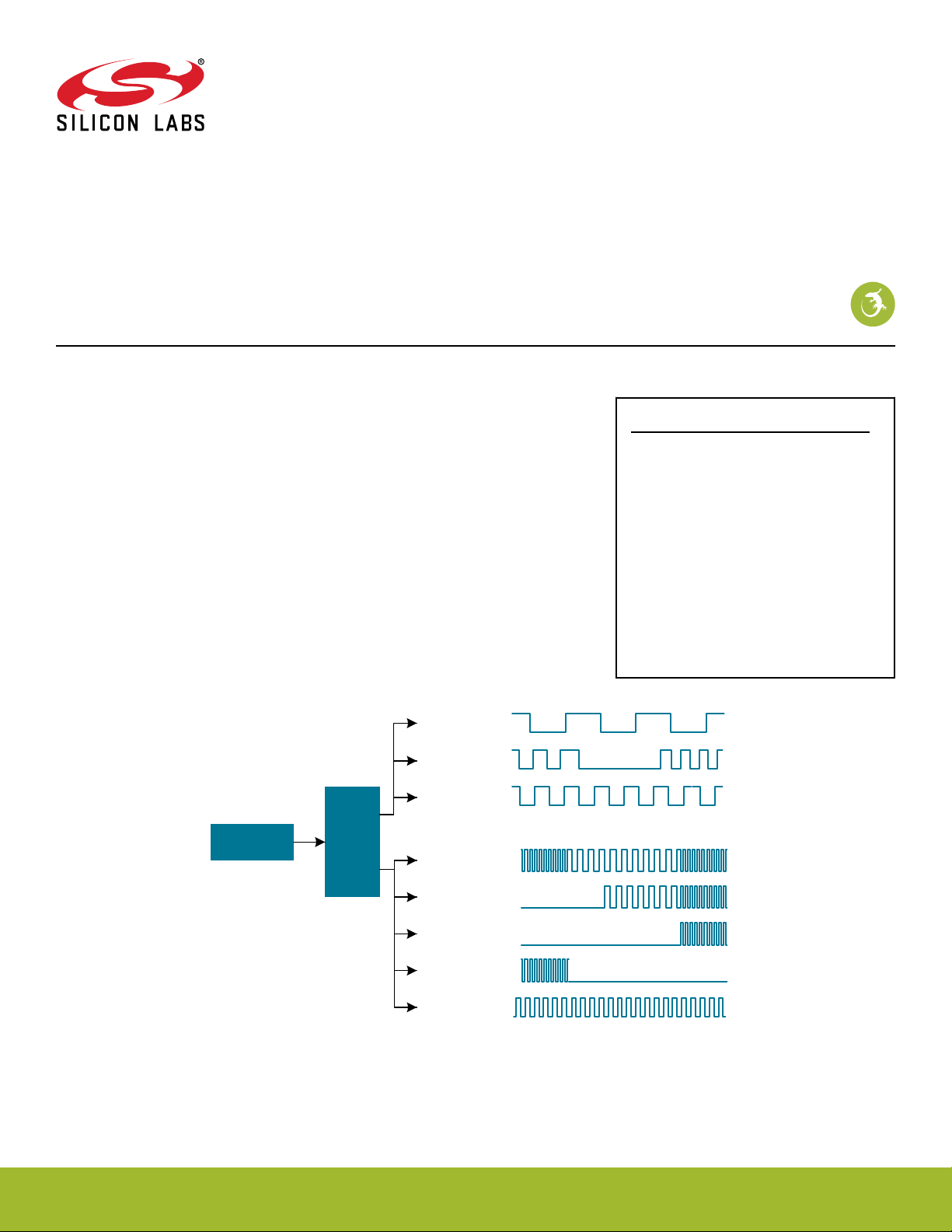
Oscillators
CMU
WDOG clock
LETIMER
clock
LCD clock
Peripheral A
clock
Peripheral B
clock
Peripheral C
clock
Peripheral D
clock
CPU clock
silabs.com | Building a more connected world. Rev. 1.12
Page 2

AN0004.1: EFM32 Series 1 and EFR32 Wireless MCU Clock Management Unit (CMU)
1. Device Compatibility
This application note supports multiple device families, and some functionality is different depending on the device.
EFM32 Series 1 consists of:
• EFM32 Jade Gecko (EFM32JG1/EFM32JG12)
• EFM32 Pearl Gecko (EFM32PG1/EFM32PG12)
• EFM32 Giant Gecko (EFM32GG11)
EFR32 Wireless Gecko Series 1 consists of:
• EFR32 Blue Gecko (EFR32BG1/EFR32BG12/EFR32BG13)
• EFR32 Flex Gecko (EFR32FG1/EFR32FG12/EFR32FG13)
• EFR32 Mighty Gecko (EFR32MG1/EFR32MG12/EFR32MG13)
Device Compatibility
silabs.com | Building a more connected world. Rev. 1.12 | 2
Page 3

AN0004.1: EFM32 Series 1 and EFR32 Wireless MCU Clock Management Unit (CMU)
Functional Description
2. Functional Description
The Clock Management Unit (CMU) controls the oscillators and clocks. It can enable or disable the clock to the different peripherals
individually, as well as enable, disable, or configure the available oscillators. This allows for minimizing energy consumption by disabling the clock for unused peripherals or having them run at lower frequencies.
silabs.com | Building a more connected world. Rev. 1.12 | 3
Page 4

AN0004.1: EFM32 Series 1 and EFR32 Wireless MCU Clock Management Unit (CMU)
Functional Description
2.1 Clock Branches
The CMU main and sub clock branches are described in the tables below. Some peripherals have dedicated prescalers, such as the
Low Energy peripherals. Other peripheral clocks must be prescaled at the source such that the same prescaled clock is driven to all
peripherals using that same source.
A detailed clock tree diagram can be found in the CMU chapter at the beginning of the Functional Description section of a given device's reference manual.
Table 2.1. Blue, Flex, Jade, Mighty, and Pearl Gecko Clock Branches
Main Clock Branch
1
Clock Source
HFCLK HFSRCCLK
• HFRCO
• HFXO
• LFRCO
• LFXO
• HFRCODIV2
• CLKIN0
2
Sub-clock Branch 1
HFPERCLK
1
Sub-clock Branch 2
1
• ACMP0, ACMP1
• ADC0
• CRYOTIMER
• CSEN
• IDAC0
• I2C0, I2C1
• TIMER0, TIMER1
• TRNG0
• USART0, USART1,
USART2, USART3
• WTIMER0, WTIMER1
• VDAC0
HFCORECLK CORTEX (Core)
HFEXPCLK —
HFBUSCLK • CRYPTO0, CRYPTO1
• GPCRC
• GPIO
• LDMA
• LE
• PRS
DBGCLK —
HFRADIOCLK • AGC
• BUFC
• CRC
• FRC
• MODEM
• PROTIMER
• RAC
• RFSENSE
• SYNTH
Radio Transceiver HFXO — —
F
(DPLL) • HFXO
ref
— —
• CLKIN0
• LFXO
silabs.com | Building a more connected world. Rev. 1.12 | 4
Page 5

AN0004.1: EFM32 Series 1 and EFR32 Wireless MCU Clock Management Unit (CMU)
Functional Description
Main Clock Branch
1
Clock Source
2
Sub-clock Branch 1
1
Sub-clock Branch 2
AUXCLK AUXHFRCO ADC_CLK —
DBGCLK
LESENSE —
MSC —
LFACLK • LFRCO
• LFXO
• ULFRCO
LFBCLK • HFCLKLE (HFBUSCLKLE/2
or /4)
• LFRCO
• LESENSE
• LETIMER0
• PCNT
• CSEN
• LEUART0
• SYSTICK
—
—
• LFXO
• ULFRCO
LFECLK • LFRCO
RTCC —
• LFXO
• ULFRCO
WDOGCLK • HFRCORECLK
CORETEX
WDOG —
• LFRCO
• LFXO
• ULFRCO
1
CRYOCLK • LFRCO
CRYOTIMER —
• LFXO
• ULFRCO
RFSENSECLK • RF Detector Clock
RFSENSE —
• LFRCO
• LFXO
• ULFRCO
Note:
1. Not all main and sub clock branches are available on a given device. Refer to the device reference manual and data sheet for
details
2. Not all clock sources for main clock branches are available on a given device. Refer to the device reference manual and data
sheet for details.
silabs.com | Building a more connected world. Rev. 1.12 | 5
Page 6

AN0004.1: EFM32 Series 1 and EFR32 Wireless MCU Clock Management Unit (CMU)
Table 2.2. Giant Gecko Series 1 Clock Branches
Functional Description
Main Clock Branch
1
Clock Source
HFCLK HFSRCCLK
• HFRCO
• HFXO
• LFRCO
• LFXO
• HFRCODIV2
• USHFRCO
• CLKIN0
2
Sub-clock Branch 1
1
Sub-clock Branch 2
1
HFPERCLK • ADC0
• CAN0, CAN1
• TIMER1, TIMER2, TIMER3
TIMER4, TIMER5, TIMER6
• TRNG0
• UART0, UART1
• USART0, USART1,
USART3, USART4, USART5
• WTIMER0, WTIMER1, WTIMER2, WTIMER3
HFPERBCLK • TIMER0
• USART2
HFPERCCLK • ACMP0, ACMP1, ACMP2,
ACMP3
• ADC0, ADC1
• CRYOTIMER
• CSEN
• IDAC0
• I2C0, I2C1, I2C2
• VDAC0
F
(DPLL) • HFXO
ref
• LFXO
• USHFRCO
• CLKIN0
HFCORECLK CORTEX (Core)
HFEXPCLK —
HFBUSCLK
• CRYPTO0
• EBI
• ETH
• GPCRC
• GPIO
• LDMA
• LE
• PRS
• QSPI0
• SDIO
• USB
DBGCLK —
— —
silabs.com | Building a more connected world. Rev. 1.12 | 6
Page 7

AN0004.1: EFM32 Series 1 and EFR32 Wireless MCU Clock Management Unit (CMU)
Functional Description
Main Clock Branch
1
Clock Source
2
Sub-clock Branch 1
1
Sub-clock Branch 2
AUXCLK AUXHFRCO ADC0_CLK —
ADC1_CLK —
DBGCLK
LESENSE —
MSC —
QSPI0_CLK —
SDIO_CLK —
LFACLK • LFRCO
• LFXO
• ULFRCO
• LCD
• LESENSE
• LETIMER0, LETIMER1
—
• PCNT
• RTC
LFBCLK • HFCLKLE (HFBUSCLKLE/2
or /4)
• LFRCO
• CSEN
• LEUART0, LEUART1
• SYSTICK
—
• LFXO
• ULFRCO
1
LFCCLK • LFRCO
USB —
• LFXO
• ULFRCO
LFECLK • LFRCO
RTCC —
• LFXO
• ULFRCO
WDOGnCLK • HFRCORECLK
CORETEX
WDOGn —
• LFRCO
• LFXO
• ULFRCO
CRYOCLK • LFRCO
CRYOTIMER —
• LFXO
• ULFRCO
Note:
1. Not all main and sub clock branches are available on a given device. Refer to the device reference manual and data sheet for
details
2. Not all clock sources for main clock branches are available on a given device. Refer to the device reference manual and data
sheet for details.
silabs.com | Building a more connected world. Rev. 1.12 | 7
Page 8

AN0004.1: EFM32 Series 1 and EFR32 Wireless MCU Clock Management Unit (CMU)
Functional Description
2.2 Clock Sources
There are a maximum of eight oscillators that can be used as clock sources for different purposes. The HFCLK is usually clocked by
the HFXO or HFRCO, whereas low energy peripherals are usually clocked by the LFXO, LFRCO, or ULFRCO. The AUXHFRCO is
typically used for the LESENSE, ADC asynchronous mode, flash programming, and the SWO debug output. The USHFRCO is intended primarily for the USB controller on Giant Gecko Series 1 but can also drive the HFCLK, if needed.
Table 2.3. Clock Sources
Oscillator Frequency Range
HFXO
HFRCO
AUXHFRCO
USHFRCO
38 – 40 MHz1 or 4 to 50 MHz
1 – 38 MHz1 or 72 MHz
1 – 381 MHz or 1 – 50 MHz
1 – 50 MHz
LFXO 32768 Hz
LFRCO 32768 Hz
ULFRCO 1000 Hz
2
2
2
2
Note:
1. EFM32xG1 and EFR32xG1/xG12/xG13
2. Giant Gecko Series 1 only
To select the clock source for a branch (e.g. HFCLK, LFA, or LFB), the chosen oscillator must be enabled before it is selected as the
clock source. If this is not done, the modules that are running from that clock branch will stop. In the case of selecting a disabled oscillator for the HFCLK branch, the CPU will stop and can only be recovered after a reset.
After a reset, the HFCLK branch is clocked by the HFRCO at the default 19 MHz frequency band, and all low frequency branches are
disabled.
Emlib has functions to enable or disable an oscillator and select it as a clock source.
Table 2.4. emlib Functions for Oscillator Enable, Disable and Selection
emlib Function Usage Example
CMU_OscillatorEnable(CMU_Osc_
TypeDef osc, bool enable, bool
wait)
Select which oscillator to enable or disable
and if it should wait for the oscillator to stabilize before returning.
Enable HFXO and wait for it to stabilize:
CMU_OscillatorEnable (cmuOsc_HFXO,
true, true);
Disable HFRCO:
CMU_OscillatorEnable (cmuOsc_HFRCO,
false, false);
CMU_ClockSelectSet(CMU_Clock_
TypeDef clock, CMU_Select_TypeDef
ref)
• Enables the chosen clock source in
case it has not been enabled yet.
• The clock parameter is one of the main
clock branches, and the ref parameter
is one of the clock sources for the selected clock branch.
Select HFXO as the source of HFCLK:
CMU_ClockSelectSet (cmuClock_HF,
cmuSelect_HFXO);
Select LFXO as the source of LFACLK:
CMU_ClockSelectSet(cmuClock_LFA,
cmuSelect_LFXO);
silabs.com | Building a more connected world. Rev. 1.12 | 8
Page 9

AN0004.1: EFM32 Series 1 and EFR32 Wireless MCU Clock Management Unit (CMU)
Functional Description
2.2.1 Clock Input from a Pin
It is possible to configure the CMU to use an external clock input on the CLKIN0 pin. This clock can be selected as the HFSRCCLK and
as the DPLL reference using the CMU_HFCLKSEL and CMU_DPLLCTRL registers, respectively. The input pin must be enabled in the
CMU_ROUTEPEN register, and the pin location is selected by the CLKIN0LOC bit field in the CMU_ROUTELOC1 register.
Note: This feature is not available on EFM32xG1 and EFR32xG1 devices.
2.3 Oscillator Configuration
2.3.1 HFXO
The High Frequency Crystal Oscillator (HFXO) is configured to ensure safe startup and operation for most common crystals by default.
In order to optimize startup time and power consumption for a given crystal, it is possible to adjust certain oscillator parameters. For
more information, refer to application note, AN0016: Oscillator Design Considerations.
The HFXO (38 MHz - 40 MHz) needs to be configured to ensure safe startup for the given crystal. The HFXO includes on-chip tunable
capacitance, which can replace external load capacitors.
Upon enabling the HFXO, a hardware state machine sequentially applies the configurable startup state and steady state control settings from the CMU_HFXOSTARTUPCTRL and CMU_HFXOSTEADYSTATECTRL registers. Please refer to the device reference manual for the detailed CMU HFXO control state machine flow.
Both the startup state and the steady state of the HFXO require configuration. After reaching the steady operating state, the HFXO
configuration can optionally be further tuned to minimize noise and current consumption.
Optimization for noise can be performed using an automatic Peak Detection Algorithm (PDA). Optimization for current can be performed after running the PDA by an automatic Shunt Current Optimization algorithm (SCO). HFXO operation is possible without running
PDA and SCO at the cost of higher noise and current consumption than is necessary.
Fixed frequency clock sources (e.g. the HFXO or CLKIN) must be disabled if voltage scaling is used (not availble on EFM32xG1 and
EFR32xG1 devices) and the frequency of such sources exceeds the maximum supported system frequency.
Table 2.5. HFXO Configuration
Configuration and Optimization Bit Field and Register
Configurable startup state Bit fields in CMU_HFXOSTARTUPCTRL
Configurable Steady State Bit fields in CMU_HFXOSTEADYSTATECTRL
Optimization for Noise (PDA)
1
Optimization for Current (SCO)
1
PEAKDETSHUNTOPTMODE bit field in CMU_HFXOCTRL
PEAKDETSHUNTOPTMODE bit field in CMU_HFXOCTRL
Note:
1. The manual PDA and SCO modes are not recommended for general use. PDA should not be used with an external clock source.
silabs.com | Building a more connected world. Rev. 1.12 | 9
Page 10

AN0004.1: EFM32 Series 1 and EFR32 Wireless MCU Clock Management Unit (CMU)
Functional Description
2.3.1.1 Using emlib for HFXO Configuration
Emlib has structures and functions that simplify configuration of the HFXO for efficient operation. Use of emlib is strongly recommended
for this reason and also in order to avoid or workaround errata related to the HFXO.
Initialization of the HFXO depends on the structure of type CMU_HFXOInit_TypeDef:
typedef struct
{
#if defined( _CMU_HFXOCTRL_MASK )
bool lowPowerMode; /**< Enable low-power mode */
bool autoStartEm01; /**< @deprecated Use @ref CMU_HFXOAutostartEnable instead. */
bool autoSelEm01; /**< @deprecated Use @ref CMU_HFXOAutostartEnable instead. */
bool autoStartSelOnRacWakeup; /**< @deprecated Use @ref CMU_HFXOAutostartEnable instead. */
uint16_t ctuneStartup; /**< Startup phase CTUNE (load capacitance) value */
uint16_t ctuneSteadyState; /**< Steady-state phase CTUNE (load capacitance) value */
uint8_t regIshSteadyState; /**< Shunt steady-state current */
uint8_t xoCoreBiasTrimStartup; /**< Startup XO core bias current trim */
uint8_t xoCoreBiasTrimSteadyState; /**< Steady-state XO core bias current trim */
uint8_t thresholdPeakDetect; /**< Peak detection threshold */
uint8_t timeoutShuntOptimization; /**< Timeout - shunt optimization */
uint8_t timeoutPeakDetect; /**< Timeout - peak detection */
uint8_t timeoutSteady; /**< Timeout - steady-state */
uint8_t timeoutStartup; /**< Timeout - startup */
#else
uint8_t boost; /**< HFXO Boost, 0=50% 1=70%, 2=80%, 3=100% */
uint8_t timeout; /**< Startup delay */
bool glitchDetector; /**< Enable/disable glitch detector */
#endif
CMU_OscMode_TypeDef mode; /**< Oscillator mode */
} CMU_HFXOInit_TypeDef;
Structure members can be set by the user, otherwise the default structures CMU_HFXOINIT_DEFAULT and
CMU_HFXOINIT_EXTERNAL_CLOCK can be used as templates for HFXO initialization.
#if defined( _EFR_DEVICE )
#define CMU_HFXOINIT_DEFAULT \
{ \
false, /* Low-noise mode for EFR32 */ \
false, /* @deprecated no longer in use */ \
false, /* @deprecated no longer in use */ \
false, /* @deprecated no longer in use */ \
_CMU_HFXOSTARTUPCTRL_CTUNE_DEFAULT, \
_CMU_HFXOSTEADYSTATECTRL_CTUNE_DEFAULT, \
_CMU_HFXOSTEADYSTATECTRL_REGISH_DEFAULT, \
0x20, /* Matching errata fix in CHIP_Init() */ \
0x7, /* Recommended steady-state XO core bias current */ \
0x6, /* Recommended peak detection threshold */ \
_CMU_HFXOTIMEOUTCTRL_SHUNTOPTTIMEOUT_DEFAULT, \
0xA, /* Recommended peak detection timeout */ \
0x4, /* Recommended steady timeout */ \
_CMU_HFXOTIMEOUTCTRL_STARTUPTIMEOUT_DEFAULT, \
cmuOscMode_Crystal, \
}
#else /* EFM32 device */
#define CMU_HFXOINIT_DEFAULT \
{ \
true, /* Low-power mode for EFM32 */ \
false, /* @deprecated no longer in use */ \
false, /* @deprecated no longer in use */ \
false, /* @deprecated no longer in use */ \
_CMU_HFXOSTARTUPCTRL_CTUNE_DEFAULT, \
_CMU_HFXOSTEADYSTATECTRL_CTUNE_DEFAULT, \
_CMU_HFXOSTEADYSTATECTRL_REGISH_DEFAULT, \
0x20, /* Matching errata fix in CHIP_Init() */ \
0x7, /* Recommended steady-state osc core bias current */ \
0x6, /* Recommended peak detection threshold */ \
_CMU_HFXOTIMEOUTCTRL_SHUNTOPTTIMEOUT_DEFAULT, \
0xA, /* Recommended peak detection timeout */ \
0x4, /* Recommended steady timeout */ \
_CMU_HFXOTIMEOUTCTRL_STARTUPTIMEOUT_DEFAULT, \
silabs.com | Building a more connected world. Rev. 1.12 | 10
Page 11

AN0004.1: EFM32 Series 1 and EFR32 Wireless MCU Clock Management Unit (CMU)
Functional Description
cmuOscMode_Crystal, \
}
#endif /* _EFR_DEVICE */
#define CMU_HFXOINIT_EXTERNAL_CLOCK \
{ \
true, /* Low-power mode */ \
false, /* @deprecated no longer in use */ \
false, /* @deprecated no longer in use */ \
false, /* @deprecated no longer in use */ \
0, /* Startup CTUNE=0 recommended for external clock */ \
0, /* Steady CTUNE=0 recommended for external clock */ \
_CMU_HFXOSTEADYSTATECTRL_REGISH_DEFAULT, \
0, /* Startup IBTRIMXOCORE=0 recommended for external clock */ \
0, /* Steady IBTRIMXOCORE=0 recommended for external clock */ \
0x6, /* Recommended peak detection threshold */ \
_CMU_HFXOTIMEOUTCTRL_SHUNTOPTTIMEOUT_DEFAULT, \
0x0, /* Peak-detect not recommended for external clock usage */ \
_CMU_HFXOTIMEOUTCTRL_STEADYTIMEOUT_2CYCLES, /* Minimal steady timeout */ \
_CMU_HFXOTIMEOUTCTRL_STARTUPTIMEOUT_2CYCLES, /* Minimal startup timeout */ \
cmuOscMode_External, \
}
The HFXO initialization structure is used as an argument when calling the CMU_HFXOInit(const CMU_HFXOInit_TypeDef *hfxoInit)
function, which writes the HFXO initialization parameters to the relevant CMU registers. After calling this function call, the HFXO can be
enabled and selected as the source of HFCLK as shown below.
/* Initialize HFXO with specific parameters */
CMU_HFXOInit_TypeDef hfxoInit = CMU_HFXOINIT_DEFAULT;
CMU_HFXOInit(&hfxoInit);
/* Enable and set HFXO for HFCLK */
CMU_ClockSelectSet(cmuClock_HF, cmuSelect_HFXO);
2.3.2 LFXO
The Low Frequency Crystal Oscillator (LFXO) is configured to ensure safe startup and operation for most common crystals by default.
In order to optimize startup time and power consumption for a given crystal, it is possible to adjust certain oscillator parameters. For
more information, refer to application note, AN0016: Oscillator Design Considerations.
The LFXO includes on-chip tunable capacitance, which can replace external load capacitors. The LFXO is configured by bit fields in the
CMU_LFXOCTRL register. Note that these bit fields should set only during initialization and are not be changed while the LFXO is enabled.
Table 2.6. CMU_LFXOCTRL Register for LFXO Configuration
Bit Field Usage
GAIN Adjusts the oscillator startup gain .
TUNING Tunes the internal load capacitance connected between LFXTAL_P and ground and LFXTAL_N and ground
symmetrically.
HIGHAMPL Setting this bit drives the crystal with a higher amplitude waveform, which in turn provides safer operation,
somewhat improves duty cycle, and lowers sensitivity to noise at the cost of increased current consumption.
AGC Setting this bit enables Automatic Gain Control, which limits the amplitude of the driving waveform in order to
reduce current draw. When AGC is disabled, the LFXO runs at the startup current, and the crystal will oscillate
rail to rail, providing safer operation, improved duty cycle, and lower sensitivity to noise at the cost of increased
current consumption.
BUFCUR The default value is intended to cover all use cases and reprogramming is not recommended.
CUR The default value is intended to cover all use cases and reprogramming is not recommended.
2.3.2.1 Using emlib for LFXO Configuration
Emlib has structures and functions that simplify configuration of the LFXO for efficient operation. Use of emlib is strongly recommended
for this reason and also in order to avoid or workaround errata related to the LFXO.
silabs.com | Building a more connected world. Rev. 1.12 | 11
Page 12

AN0004.1: EFM32 Series 1 and EFR32 Wireless MCU Clock Management Unit (CMU)
Functional Description
Initialization of the LFXO depends on the structure of type CMU_LFXOInit_TypeDef:
typedef struct
{
#if defined( _CMU_LFXOCTRL_MASK )
uint8_t ctune; /**< CTUNE (load capacitance) value */
uint8_t gain; /**< Gain / max startup margin */
#else
CMU_LFXOBoost_TypeDef boost; /**< LFXO boost */
#endif
uint8_t timeout; /**< Startup delay */
CMU_OscMode_TypeDef mode; /**< Oscillator mode */
} CMU_LFXOInit_TypeDef;
Structure members can be set by the user, otherwise the default structures CMU_LFXOINIT_DEFAULT and
CMU_LFXOINIT_EXTERNAL_CLOCK below can be used as templates for LFXO initialization.
#define CMU_LFXOINIT_DEFAULT \
{ \
_CMU_LFXOCTRL_TUNING_DEFAULT, /* Default CTUNE value, 0 */ \
_CMU_LFXOCTRL_GAIN_DEFAULT, /* Default gain, 2 */ \
_CMU_LFXOCTRL_TIMEOUT_DEFAULT, /* Default start-up delay, 32k cycles */ \
cmuOscMode_Crystal, /* Crystal oscillator */ \
}
#define CMU_LFXOINIT_EXTERNAL_CLOCK \
{ \
0, /* No CTUNE value needed */ \
0, /* No LFXO startup gain */ \
_CMU_LFXOCTRL_TIMEOUT_2CYCLES, /* Minimal lfxo start-up delay, 2 cycles */ \
cmuOscMode_External, /* External digital clock */ \
}
The LFXO initialization structure is used as an argument when calling the CMU_LFXOInit(const CMU_LFXOInit_TypeDef *lfxoInit)
function, which writes the LFXO initialization parameters to the relevant CMU registers. After calling this function, the LFXO can be
enabled and selected as the clock source for low energy peripherals.
/* Initialize LFXO with specific parameters */
CMU_LFXOInit_TypeDef lfxoInit = CMU_LFXOINIT_DEFAULT;
CMU_LFXOInit(&lfxoInit);
/* Enable and set LFXO for LFACLK */
CMU_ClockSelectSet(cmuClock_LFA, cmuSelect_LFXO);
silabs.com | Building a more connected world. Rev. 1.12 | 12
Page 13

AN0004.1: EFM32 Series 1 and EFR32 Wireless MCU Clock Management Unit (CMU)
Functional Description
2.3.3 HFRCO, AUXHFRCO, and USHFRCO
The HFRCO, AUXHFRCO, and USHFRCO (available on Giant Gecko Series 1 only) default to operation in the 19 MHz band but can
be switched to operate in one of the other preset frequency bands by changing the FREQRANGE bit field in the CMU_HFRCOCTRL,
CMU_AUXHFRCOCTRL, or CMU_USHFRCOCTRL registers. The USHFRCO (Universal HFRCO) is functionally identical to the
AUXHFRCO and can provide the clock for the QSPI, SDIO, or USB independent of the HFSRCCLK.
Table 2.7. High Frequency RC Oscillator Band Selection
Oscillator Frequency Band
AUXHFRCO
HFRCO
• 1 MHz (DIV4 from 4 MHz)
• 2 MHz (DIV2 from 4 MHz)
• 4 MHz
• 7 MHz
• 13 MHz
• 16 MHz
• 19 MHz (Default)
• 26 MHz
• 32 MHz
• 38 MHz
• 48 MHz (Giant Gecko Series 1 only)
• 50 MHz (Giant Gecko Series 1 only)
• 1 MHz (DIV4 from 4 MHz)
• 2 MHz (DIV2 from 4 MHz)
• 4 MHz
• 7 MHz
• 13 MHz
• 16 MHz
• 19 MHz (Default)
• 26 MHz
• 32 MHz
• 38 MHz
• 48 MHz (Giant Gecko Series 1 only)
• 56 MHz (Giant Gecko Series 1 only)
• 64 MHz (Giant Gecko Series 1 only)
• 72 MHz (Giant Gecko Series 1 only)
USHFRCO (Giant Gecko Series 1 only)
• 1 MHz (DIV4 from 4 MHz)
• 2 MHz (DIV2 from 4 MHz)
• 4 MHz
• 7 MHz
• 13 MHz
• 16 MHz
• 19 MHz (Default)
• 26 MHz
• 32 MHz
• 38 MHz
• 48 MHz
• 50 MHz
The specific values that select each tuning band are written to the TUNING bit field in the CMU_HFRCOCTRL and CMU_AUXHFRCOCTRL registers. Each band is calibrated during production, with suitable tuning values written to the Device Information (DI) page.
The HFRCO and AUXHFRCO frequency can be more accurately tuned at the cost of increased current consumption via the FINETUNING and FINETUNINGEN bit fields in the CMU_HFRCOCTRL and CMU_AUXHFRCOCTRL registers.
silabs.com | Building a more connected world. Rev. 1.12 | 13
Page 14

AN0004.1: EFM32 Series 1 and EFR32 Wireless MCU Clock Management Unit (CMU)
Functional Description
When Voltage Scaling is used (not available on EFM32xG1 and EFR32xG1 devices), the HFRCO and AUXHFRCO must be tuned to
frequencies that do not exceed the maximum system frequency permitted with scaling before voltage scaling is actually applied.
Emlib has specific functions to change the frequency band to which the AUXHFRCO and HFRCO are tuned. Use of emlib is strongly
recommended because it specifically handles the need to increase the number of flash wait states or voltage scaling when a higher
frequency tuning band is selected. These functions switch to the desired frequency band by loading the correct tuning value from the
Device Information (DI) page.
Table 2.8. emlib Functions for Changing the AUXHFRCO and HFRCO Tuning Bands
emlib Function Usage Example
CMU_HFRCOBandSet(CMU_HFRCOFreq_
TypeDef setFreq)
CMU_AUXHFRCOBandSet(CMU_
AUXHFRCOFreq_TypeDef setFreq)
Change HFRCO frequency band. CMU_HFRCOBandSet(cmuHFRCOFreq_26M0Hz);
Change AUXHFRCO frequency
band.
CMU_
AUXHFRCOBandSet(cmuAUXHFRCOFreq_13M0Hz);
2.3.4 LFRCO
It is possible to calibrate the LFRCO to achieve higher accuracy. The frequency is adjusted by changing the TUNING bi tfield in the
CMU_LFRCOCTRL register. The LFRCO is also calibrated in production, and its default TUNING value is set during reset.
Voltage reference duty cycling can be enabled for the LFRCO by setting the ENVREF bit in the CMU_LFRCOCTRL register before
enabling the LFRCO. This reduces current consumption at the expense of slightly worse frequency accuracy, especially at high temperatures. Comparator chopping and dynamic element matching are enabled with the ENCHOP and ENDEM bits in the
CMU_LFRCOCTRL register, which improves the average LFRCO frequency accuracy at the cost of reduced cycle-to-cycle accuracy
(increased jitter).
2.3.5 ULFRCO
The ULFRCO is always on in EM0, EM1, EM2, EM3 and EM4H and cannot be disabled via the CMU_OSCENCMD register. As such, it
is always available as a clock source for many of the peripherals in the low-frequency clock domains. It is not possible to calibrate the
ULFRCO to achieve higher accuracy.
silabs.com | Building a more connected world. Rev. 1.12 | 14
Page 15

AN0004.1: EFM32 Series 1 and EFR32 Wireless MCU Clock Management Unit (CMU)
Functional Description
2.4 Oscillator Start-Up Time and Time-Out
The start-up time for each of the previously discussed oscillators differs and, in certain cases, can be further extended by one or more
programmable time-out delays. When enabled, the oscillator's output is given time to stabilize by stalling assertion of its ready signal for
the specified number of clock cycles. Low start-up times can be selected when the clock is coming from a high quality source, while
longer time-out delays are necessary when the clock is coming directly from a crystal.
Programmable time-outs are available for the LFXO, HFXO, and LFRCO. The HFRCO, AUXHFRCO, ULFRCO, and USHFRCO timeout delays are fixed and cannot be changed.
Table 2.9. Oscillator Time-Out Configuraton
Oscillator Bit Field Register
LFXO TIMEOUT CMU_LFXOCTRL
HFXO • STARTUPTIMEOUT
CMU_HFXOTIMEOUTCTRL
• STEADYTIMEOUT
• PEAKDETTIMEOUT
• SHUNTOPTTIMEOUT
LFRCO TIMEOUT CMU_LFRCOCTRL
HFRCO Start-up time is fixed.
AUXHFRCO Start-up time is fixed.
ULFRCO Start-up time is fixed.
USHFRCO Start-up time is fixed.
2.4.1 HFXO Deterministic Start-up Time
A second time-out counter allows the HFXO to achieve deterministic start-up timing based on the LFXO, ULFRCO, or LFRCO. It runs
off the LFECLK and can even be used during wake-up from EM2 when either the ULFRCO, LFRCO, or LFXO is already running and
stable (see 5.2.3 Automatic HFXO Start with Deterministic Start-Up).
When enabled, this counter delays HFXO ready assertion by the number of LFECLK cycles specified by the LFTIMEOUT bit field in the
CMU_HFXOCTRL register. The HFXO ready signal is asserted when the time-out counters configured via the CMU_HFXOTIMEOUTCTRL register and the LFTIMEOUT counter have both elapsed. If the LFTIMEOUT countdown completes first, the LFTIMEOUTERR bit in CMU_IF will be set. Note that use of LFTIMEOUT requires the peripheral causing the wake-up from EM2 to reside in the
LFECLK domain.
silabs.com | Building a more connected world. Rev. 1.12 | 15
Page 16

AN0004.1: EFM32 Series 1 and EFR32 Wireless MCU Clock Management Unit (CMU)
Functional Description
2.5 Prescaling
Each of the clock sub-branches derived from the HFCLK, such as the HFCORECLK, HFBUSCLK, and HFPERCLK, can be individually
prescaled by a factor of 1 to 512, while the HFCLK itself can be divided down by a value between 1 and 32. The HFCORECLK drives
the CPU and modules tightly coupled to it like the flash (MSC) and SRAM. The HFBUSCLK does the same for modules which can read
and write data on their own like the LDMA and USB but also for modules requiring fast response to CPU reads and writes, such as the
GPIO and external bus interface (EBI). The HFPERCLK and its branches (HFPERBCLK and HFPERCCLK) drive high-frequency peripherals like the timers and USARTs. Some peripherals permit further clock prescaling (such as the ADC), which is controlled independently in each such peripheral's register space.
Prescaling is controlled independently by dedicated bit fields for most peripherals in the low frequency clock domains (LFA, LFB, and
LFE), with the exception of the Pulse Counter (PCNT).
Table 2.10. Prescaler of Clock Branches
Clock Branch
Prescaler Bitfield
1
Prescaler Register Prescaler Range
HFCLK PRESC CMU_HFPRESC 1 to 32
HFPERCLK PRESC CMU_HFPERPRESC 1 to 512
HFPERBCLK PRESC CMU_HFPERPRESCB 1 to 512
HFPERCCLK PRESC CMU_HFPERPRESCC 1 to 512
HFRADIOCLK PRESC CMU_HFRADIOPRESC 1 to 512
HFCORECLK PRESC CMU_HFCOREPRESC 1 to 512
HFEXPCLK PRESC CMU_HFEXPPRESC 1 to 512
LFACLK LCD CMU_LFAPRESC0
LESENSE
LETIMER0, LETIMER1
RTC
LFBCLK CSEN CMU_LFBPRESC0
LEUART0, LEUART1
SYSTICK
LFECLK RTCC CMU_LFEPRESC0
20 to 2
20 to 2
20 to 2
20 to 2
24 to 2
20 to 2
0
2
20 or 20 to 2
7
3
15
15
7
3
2
Note:
1. Not all prescaler bitfields are available on a given device. Refer to the device reference manual and data sheet for details.
Emlib has functions to set the clock prescalers, and its use is highly encouraged because synchronization is required for prescalers in
the low frequency clock domains.
Table 2.11. emlib Clock Divider and Prescaler Functions
emlib Function Divider/Prescaler Example
CMU_ClockDivSet(CMU_Clock_TypeDef
clock, CMU_ClkDiv_TypeDef div)
CMU_ClockPrescSet(CMU_Clock_TypeDef
clock, uint32_t presc)
silabs.com | Building a more connected world. Rev. 1.12 | 16
One of the enumerated power-of-2 dividers
of type CMU_ClkDiv_TypeDef
Divide by 32768 (215) for LETIMER0:
CMU_ClockDivSet(cmuClock_LETIMER0,
cmuClkDiv_32768);
An integer prescaler between 1 and 512 HFPERCLK divide by 6:
CMU_ClockDivSet(cmuClock_HFPER, 6);
Page 17

AN0004.1: EFM32 Series 1 and EFR32 Wireless MCU Clock Management Unit (CMU)
Functional Description
When using these functions, careful consideration is required for both parameters. Not all clocks have a prescaler, and the maximum
prescaling value is also not the same for the different clocks (HFPERCLK, for instance, has a maximum of 512 while the LETIMER
clocks can be divided by 32768).
2.6 Flash Wait States
When increasing the memory subsystem clock (HFCLK) frequency above certain limits, the number of wait states required for flash
read accesses must be increased before the frequency change is performed. Likewise, the number of wait states can be reduced when
the HFCLK frequency falls below certain limits, and this must be perfomred after the frequency change has taken place. Wait state and
frequency changes are properly sequenced and handled automatically by emlib's CMU functions, and their use is strongly encouraged.
Changes to the number of wait states can be made under user control directly by writing to the MODE bit field in the MSC_READCTRL
register.
Table 2.12. Flash Wait States for EFM32xG1 and EFR32xG1
Clock Frequency Minimum Flash Wait States
HFCLK ≤ 32 MHz 0
HFCLK > 32 MHz 1
Table 2.13. Flash Wait States for EFM32xG12/13 and EFR32xG12/13
Clock Frequency Minimum Flash Wait States
HFCLK ≤ 25 MHz 0
HFCLK > 25 MHz 1
Table 2.14. Flash Wait States for Giant Gecko Series 1
Clock Frequency Minimum Flash Wait States
HFCLK ≤ 18 MHz 0
18 MHz < HFCLK ≤ 36 MHz 1
36 MHz < HFCLK ≤ 54 MHz 2
54 MHz < HFCLK ≤ 72 MHz 3
Voltage scaling (not supported on EFM32xG1 and EFR32xG1 devices) allows for a tradeoff between power and performance. The flash
wait states for voltage scaling level 0 are described in table below. Operation above 21 MHz with voltage scaling is not supported.
Table 2.15. Flash Wait States at Voltage Scaling Level 0
Clock Frequency Minimum Flash Wait States
HFCLK <= 7 MHz 0
7 MHz < HFCLK<= 14 MHz 1
14 MHz < HFCLK<= 21 MHz 2
The emlib functions below optimize flash access wait-state configuration if the source or frequency of HFCLK is changed when invoking
these functions.
• CMU_ClockDivSet(CMU_Clock_TypeDef clock, CMU_ClkDiv_TypeDef div)
• CMU_ClockPrescSet(CMU_Clock_TypeDef clock, CMU_ClkPresc_TypeDef presc)
• CMU_ClockSelectSet(CMU_Clock_TypeDef clock, CMU_Select_TypeDef ref)
• CMU_HFRCOBandSet(CMU_HFRCOFreq_TypeDef setFreq)
• CMU_HFXOAutostartEnable(uint32_t userSel, bool enEM0EM1Start, bool enEM0EM1StartSel)
silabs.com | Building a more connected world. Rev. 1.12 | 17
Page 18

AN0004.1: EFM32 Series 1 and EFR32 Wireless MCU Clock Management Unit (CMU)
Functional Description
2.7 Low Energy (LE) Peripheral Clock Divider
To use the low energy peripheral modules, the LE interface clock (HFCLKLE) must be enabled in addition to the module clock.
The HFCLKLEPRESC bitfield in the CMU_HFPRESC register is used to divide the HFBUSCLKLE frequency to ensure the HFCLKLE
frequency is within the limit.
The WSHFLE bitfield in the CMU_CTRL register is used to ensure that the Low Energy Peripheral Interface is able to operate at the
given HFBUSCLKLE frequency by inserting wait states when using this interface.
Table 2.16. Low Energy Peripheral Clock Divider
Device HFBUSCLKLE Max-
imum
• EFM32xG1
40 MHz 16 MHz • 0 or 1 if HFBUSCLKLE <= 32
• EFM32xG12
• EFR32xG1
• EFR32xG12
HFCLKLE Maximum
WSHFLE HFCLKLEPRESC
• DIV2 or DIV4 if
MHz
• 1 if HFBUSCLKLE > 32 MHz
HFBUSCLKLE <= 32 MHz
• DIV4 if HFBUSCLKLE > 32
MHz
• EFR32xG13
Before going to a high frequency, make sure the registers in the table above have the correct values. When going down in frequency,
make sure to keep the registers at the values required by the higher frequency until after the switch completes.
To make this task easier, there is also a function available in the emlib to ensure the registers in the table above have the correct values when enabling the LE clock.
Table 2.17. The emlib Function to Enable a Module Clock
emlib Function Usage Example
CMU_ClockEnable(CMU_Clock_TypeDef
clock, bool enable)
To enable a module clock. Enable LE clock with correct settings on correspond-
ing registers:
CMU_ClockEnable(cmuClock_HFLE, true);
2.8 External Clock Sources
By default, the LFXO and HFXO are started in crystal mode, but it is possible to connect an active external sine wave or square wave
clock source to the LFXTAL_N and HFXTAL_N pins of the LFXO and HFXO as discussed in the following sections.
2.8.1 External Sine Wave
An AC-coupled, externally buffered sine wave can be applied to the HFXTAL_N or LFXTAL_N pin. The amplitude of this signal must be
at least 0.8 V peak-to-peak, and the frequency is subject to the same limit as that of a crystal connected to the HFXO or LFXO.
Each oscillator has a way to be configured for use with a stimulus other than a crystal. In the case of the HFXO, the MODE bit in the
CMU_HFXOCTRL register is set to indicate that an external clock source (EXTCLK) is being used. Sine wave operation for the LFXO is
selected by the BUFEXTCLK setting of the CMU_LFXOCTRL register's MODE bit field.
2.8.2 Digital External Clock
A rail-to-rail square wave with 50% duty cycle can be applied to the HFXTAL_N or LFXTAL_N pin, subject to the same frequency limit
as that of a crystal connected to the HFXO or LFXO.
Each oscillator has a way to be configured for use with a stimulus other than a crystal. In the case of the HFXO, the MODE bit in the
CMU_HFXOCTRL register is set to indicate that an external clock source (EXTCLK) is being used. Operation with a digital external
clock for the LFXO is selected by the DIGEXTCLK setting of the CMU_LFXOCTRL register's MODE bit field.
silabs.com | Building a more connected world. Rev. 1.12 | 18
Page 19

AN0004.1: EFM32 Series 1 and EFR32 Wireless MCU Clock Management Unit (CMU)
Functional Description
2.8.3 Oscillator Pin Availability
When a clock is supplied via LFXTAL_N, the corresponding LFXTAL_P pin is not needed and can be used for GPIO or peripheral functionality. HFXTAL_P availability when not used to connect a crystal is device-dependent and can be found in the datasheet pin alternate
functionality tables.
silabs.com | Building a more connected world. Rev. 1.12 | 19
Page 20

AN0004.1: EFM32 Series 1 and EFR32 Wireless MCU Clock Management Unit (CMU)
Functional Description
2.9 Output Clock to Pin
The CMU can drive user-specified clocks on certain pins. Selection is done using the CLKOUTSELn bit fields in the CMU_CTRL register. It is also necessary to (a) select which pins are driven in the CMU_ROUTELOC0 register, (b) configure them as outputs in the appropriate GPIO pin mode registers, and (c) enable each one via its corresponding bit in the CMU_ROUTEPEN register.
Note that a clock sourced from an oscillator (e.g. the HFXO) can be unstable after startup and should not be output on a pin before its
corresponding ready flag (e.g. HFXORDY) is set in the CMU_STATUS register.
Table 2.18. Clock Output on a Pin
Pin Bit Field and Register
CMU_OUT0
CMU_OUT1
CLKOUTSEL0 in CMU_CTRL:
• ULFRCO (directly from oscillator)
• LFRCO (directly from oscillator)
• LFXO (directly from oscillator)
• HFXO (directly from oscillator)
• HFEXPCLK
• ULFRCOQ (qualified)
• LFRCOQ (qualified)
• LFXOQ (qualified)
• HFRCOQ (qualified)
• AUXHFRCOQ (qualified)
• HFXOQ (qualified)
• HFSRCCLK
•
USHFRCOQ (qualified)
1
CLKOUTSEL1 in CMU_CTRL:
• ULFRCO (directly from oscillator)
• LFRCO (directly from oscillator)
• LFXO (directly from oscillator)
• HFXO (directly from oscillator)
• HFEXPCLK
• ULFRCOQ (qualified)
• LFRCOQ (qualified)
• LFXOQ (qualified)
• HFRCOQ (qualified)
• AUXHFRCOQ (qualified)
• HFXOQ (qualified)
• HFSRCCLK
•
USHFRCOQ (qualified)
1
silabs.com | Building a more connected world. Rev. 1.12 | 20
Page 21

AN0004.1: EFM32 Series 1 and EFR32 Wireless MCU Clock Management Unit (CMU)
Pin Bit Field and Register
CMU_OUT2
1
CLKOUTSEL2 in CMU_CTRL:
• ULFRCO (directly from oscillator)
• LFRCO (directly from oscillator)
• LFXO (directly from oscillator)
• HFXODIV2Q (HFXO ÷ 2 qualified)
• HFXO (directly from oscillator)
• HFEXPCLK
• HFXOX2Q (HFXO × 2 qualified)
• ULFRCOQ (qualified)
• LFRCOQ (qualified)
• LFXOQ (qualified)
• HFRCOQ (qualified)
• AUXHFRCOQ (qualified)
• HFXOQ (qualified)
• USHFRCOQ (qualified)
Functional Description
Location
Enable
CLKOUT0LOC, CLKOUT1LOC, and CLKOUT2LOC1in CMU_ROUTELOC0
CLKOUT0PEN, CLKOUT1PEN, and CLKOUT2PEN1 in CMU_ROUTEPEN register.
Note:
1. Giant Gecko Series 1 only
2.10 Clock Output to PRS
The CMU can be used as a PRS producer with the clocks selected by the CLKOUTSEL bit fields in the CMU_CTRL register directed to
any of the PRS consumers.
Other than picking the clock(s) desired via the CLKOUTSEL bit field(s), no additional configuration of the CMU is required. Instead, a
given PRS channel routes one of the CMU clock outputs to a consumer via the SOURCESEL and SIGSEL fields in the
PRS_CHx_CTRL register.
Apart from its typical uses (e.g. for ADC conversion start timing), the PRS can be used as an enhanced clock output routing mechanism. Depending on the device, each PRS channel can be output to anywhere between 3 and 17 different pins, making it possible to
route the different CMU clock outputs to pins not otherwise made available via location bit fields in the CMU_ROUTELOC0 register.
2.11 Interrupts
The CMU can request interrupts from multiple sources that are serviced by a single interrupt vector. If CMU interrupts are enabled, an
interrupt is requested when one or more of the flags in CMU_IF register and their corresponding bits in CMU_IEN register are set.
The LFRCORDY and LFXORDY interrupts can be used to wake from EM2. In this way, waiting for either the LFRCO or LFXO to stablilize by polling its associated ready bit can be avoided by going into EM2 after enabling the oscillator and sleeping until the ready interrupt causes a wake-up.
silabs.com | Building a more connected world. Rev. 1.12 | 21
Page 22

AN0004.1: EFM32 Series 1 and EFR32 Wireless MCU Clock Management Unit (CMU)
Functional Description
2.12 Automatic HFXO Start
EFM32 and EFR32 Wireless Gecko Series 1 devices can enable the HFXO and select it as the HFSRCCLK automatically under hardware control. This is intended to minimize current draw by allowing the system to remain in a low-energy mode until the HFXO is ready
instead of having software poll the HFXORDY bit in the CMU_STATUS or CMU_IF register.
The AUTOSTARTRDYSELRAC bit in the HFXOCTRL register on the EFR32 Wireless Gecko Series 1family permits automatic HFXO
start-up and its selection as the HFSRCCLK when ready in response to the wake-up event from the Radio Controller (RAC). The CMU
documentation for these devices describes a typical use case whereby the RAC (which must run from the HFXO) periodically wakes
from EM2 to perform work and then goes back to sleep all without software intervention courtesy of this feature.
A separate mechanism controlled by the AUTOSTARTSELEM0EM1 and AUTOSTARTEM0EM1 bits in the CMU_HFXOCTRL register
performs a similar function depending on the current energy mode.
Table 2.19. Energy Mode-Dependent HFXO Start-up and HFSRCCLK Selection
AUTOSTARTSELEM0EM1 AUTOSTARTEM0EM1 Action
0 0 None. HFXO enabled in software as usual.
0 1 • Automatic start-up of the HFXO in EM0/EM1 (also after entry
from EM2/EM3).
• HFSRCCLK remains unchanged.
1 X • Automatic start-up of the HFXO in EM0/EM1 (also after entry
from EM2/EM3).
• Immediate selection of the HFXO as the HFSRCCLK
• HFSRCCLK stalled until the HFXO is ready.
When AUTOSTARTSELEM0EM1 is set to 1 in EM0/EM1 (regardless of the state of the AUTOSTARTRDYSELRAC or AUTOSTARTEM0EM1 bits), selection of the HFXO as the HFSRCCLK will occur immediately, even if HFXO is not yet ready. Upon wake-up into
EM0/EM1, this can therefore lead to a relatively long start-up time as the system will not operate from the HFRCO as it would otherwise
normally do (see 5.2.2 Automatic HFXO Start with Normal Start-Up and 5.2.3 Automatic HFXO Start with Deterministic Start-Up).
Care should be taken to ensure that the settings of the MSC_READCTRL (flash wait states) and CMU_CTRL (WSHFLE) registers are
compatible with the HFXO frequency before enabling the automatic start-up feature. This is properly handled when HFXO auto-start is
enabled using the emlib CMU_HFXOAutostartEnable() function.
silabs.com | Building a more connected world. Rev. 1.12 | 22
Page 23

AN0004.1: EFM32 Series 1 and EFR32 Wireless MCU Clock Management Unit (CMU)
Functional Description
2.13 Digital Phased-Locked Loop (DPLL)
The Digital Phase-Locked Loop (DPLL) uses a digitally controlled oscillator (DCO) and 12-bit N and M dividers as part of a feedback
mechanism that allows more accurate tuning of the HFRCO clock output.
Note: EFR32 Wireless Gecko Series 1and EFM32xG1 devices do not include the DPLL.
Table 2.20. Digital Phase-Locked Loop Operation
Item Operation
Frequency-lock loop mode (FREQLL) • Keeps the DCO frequency-locked to the reference clock, which means the
DCO frequency will be accurate.
• Phase error can accumulate over time and cause the average frequency error to be non-zero.
• FREQLL mode provides better jitter and transient performance and should
be used unless a specific phase requirement exists.
Phase-lock loop mode (PHASELL) • Keeps the DCO phase-locked to the reference clock,.
• Phase error does not accumulate over time. so the average frequency error
converges to zero.
Reference clock source (FREF) Selected by REFSEL bit field in the CMU_DPLLCTRL register:
• HFXO
• LFXO
• CLKIN0
Output frequency • Output frequency = FREF × (N+1)/(M+1), where N (must > 32) and M are
12-bit values written to the CMU_DPLLCTRL1 register.
• The DCO lock time increases and DCO jitter decreases as N increases.
• N+1 > 300 recommended as a reasonable compromise between lock time
and jitter unless a specific lock time is required.
• All configuration must be done before enabling the DPLL and must not be
changed while the DPLL is running.
Lock detection Associated interrupt flag and enable bits in the CMU_IF and CMU_IEN regis-
ters:
• DPLLRDY is set when the DPLL successfully locks to the reference clock
based on the programmed configuration.
• DPLLLOCKFAILLOW is set when DPLL fails to lock because the period lower boundary is hit.
• DPLLLOCKFAILHIGH is set when DPLL fail to lock because the period upper boundary is hit.
Output spectrum spreading The DPLL can randomize the generated output period by a configurable
amount of spread.
Enabling and disabling
• Software enable and disable bits reside in the CMU_OSCENCMD register.
• The DPLL is disabled automatically when entering EM2, EM3, EM4H or
EM4S.
• Before enabling DPLL, the HFCLK must temporarily be switched to the
HFRCODIV2 source until the DPLL is locked to avoid exceeding the maximum operating frequency due to overshoot.
• Before enabling DPLL, flash wait states must be increased if warranted by
the selected target frequency
• It is also necessary to set the FINETUNINGEN bit in the
CMU_HFRCOCTRL register to link the DPLL with the HFRCO.
• The HFRCO serves as the local oscillator for DPLL; it is also enabled/disabled when DPLL is enabled/disabled.
silabs.com | Building a more connected world. Rev. 1.12 | 23
Page 24

AN0004.1: EFM32 Series 1 and EFR32 Wireless MCU Clock Management Unit (CMU)
Energy Modes
3. Energy Modes
3.1 Active Oscillators
The energy mode of the device determines which oscillators are active. In EM0 and EM1, all oscillators can be enabled and used as
clock sources. Upon entering EM2, the high frequency oscillators (HFXO, HFRCO, AUXHFRCO, and USHFRCO, if present) shut off
automatically, such that the high frequency peripherals running from them are also effectively shutdown. In EM3, the low frequency
oscillators (LFXO and LFRCO if present) also stop, disabling the low frequency peripherals. The ULFRCO is active in all energy modes
down to EM4H and is only disabled in EM4S unless explicitly retained via the RETAINULFRCO bit in the EMU_EM4CTRL register.
The following table summarizes oscillator availability in each energy mode:
Table 3.1. Energy Mode Oscillator Availability
Oscillator Energy Mode
EM0 EM1 EM2 EM3 EM4H EM4S
HFXO Available Available — — — —
HFRCO Available Available — — — —
AUXHFRCO Available Available
On demand
1
On demand
1
— —
USHFRCO Available Available — — — —
DPLL Available Available — — — —
LFXO Available Available Available —
LFRCO Available Available Available —
Available
Available
ULFRCO On On On On On
2
3
Available
Available
Available
2
3
4
Note:
1. In response to an asynchronous ADC trigger from the PRS.
2. If retained by the RETAINLFXO bit in EMU_EM4CTRL.
3. If retained by the RETAINLFRCO bit in EMU_EM4CTRL.
4. If retained by the RETAINULFRCO bit in EMU_EM4CTRL.
3.2 Wake Up Considerations
3.2.1 Waking up from Low-Energy Modes
All the oscillators are able to run in EM1, so the core wakes up instantly from this energy mode. In EM2 and EM3 the high frequency
oscillators are disabled, and these need to be re-enabled before the core starts running code.
When waking up from EM2 or EM3, the core will run from the HFRCO by default, regardless of which oscillator it was running from
before entering these energy modes. The HFRCO has a very short wake-up time, and it takes only few microseconds before the CPU
starts running code. The previously-selected HFRCO band is also restored by hardware on wake-up. The core will run the HFRCO at
the default frequency band when waking up from EM4H or EM4S.
Note: Refer to the device-specific data sheet for the wake-up times from each energy mode.
silabs.com | Building a more connected world. Rev. 1.12 | 24
Page 25

AN0004.1: EFM32 Series 1 and EFR32 Wireless MCU Clock Management Unit (CMU)
Energy Modes
3.2.2 Restoring the Oscillator
To use an oscillator other than the HFRCO after wake-up from a low-energy mode, the user must either enable and select the oscillator
manually or use the energy mode entry functions in emlib, like EMU_EnterEM2(), which can handle this automatically.
If an oscillator (the HFXO, for instance) is manually selected as a clock source before it is stable, the system may not operate correctly.
The EMU_EnterEM2() and EMU_EnterEM3()functions in emlib have a boolean parameter that permits any previously enabled oscillators
to be restored upon wake-up (see figure below) .
When the user chooses not to restore previously enabled oscillators upon low-energy mode wake-up, any oscillator, other than the
HFRCO, that is needed must be manually enabled and selected as a clock source. When the EMU_EnterEM2() or
EMU_EnterEM3()boolean restore parameter is true, emlib will re-enable oscillators, wait for the previously selected HFCLK source to
stabilize, and re-select it as the HFCLK at the expense of additional processing time upon wake-up. If the HFRCO was disabled prior to
low-energy mode entry (e.g. the HFCLK was sourced from the HFXO), emlib will also disable it after restoring the previously selected
HFCLK source.
If restore is false:
· HFCLK will be HFRCO
· Processing time is
proportional to wake
up time
If restore is true:
· HFCLK will be the
same prior to EM2/3
· Processing time is
proportional to start-up
time and inversely
proportional to
oscillator speed
EM0
EMU_EnterEM2(bool restore)
or
EMU_EnterEM3(bool restore)
EM2/3
Figure 3.1. Oscillator restoring
The LFXO and HFXO have programmable start-up delays that are set in software by bit fields in each oscillator's respective control
registers (see Table 2.9 Oscillator Time-Out Configuraton on page 15). These bit fields specify the number of cycles that must elapse
before the oscillator's ready flag is set and can be adjusted to match the characteristics of a particular crystal (faster or slower start-up).
A longer time-out (e.g. 16K cycles) guarantees oscillator stability but also extends the period after wake-up spent polling the oscillator's
ready flag. For a 32 MHz crystal, a time-out of 16K translates into an approximate delay of 500 µs between the HFXO starting up and
its ready flag being set. A lower time-out results in the ready flag setting sooner, but with the risk that the oscillator might not yet be
stable.
Each oscillator's ready flag can also be enabled as an interrupt request, the benefit of which is that the processor can continue running
code after enabling an oscillator without the need for polling. This is particularly useful when the HFXO provides the HFCLK. Instead of
using the EMU_EnterEM2() or EMU_EnterEM3() restore capability, the HFXO ready interrupt can be enabled prior to entering EM2 or
EM3. Upon wake-up, software can manually restart the HFXO and continue running code with the HFCLK still sourced from the
HFRCO, only switching to the HFXO when the ready interrupt is eventually requested.
silabs.com | Building a more connected world. Rev. 1.12 | 25
Page 26

AN0004.1: EFM32 Series 1 and EFR32 Wireless MCU Clock Management Unit (CMU)
RC Oscillator Calibration
4. RC Oscillator Calibration
The CMU has built-in hardware support to efficiently calibrate the RC oscillators at run-time by comparing the RC oscillator frequency
with a selected reference clock. When the calibration circuit is started, one down-counter running from a selectable clock (DOWNSEL
bit field in the CMU_CALCTRL register) and one up-counter running from another selectable clock (UPSEL bit field in the
CMU_CALCTRL register) are started simultaneously.
When the down-counter has reached 0, the up-counter is sampled and the CALRDY interrupt flag is set. If the CONT bit in the
CMU_CALCTRL register is cleared, the counters are stopped after finishing the ongoing calibration. Continuous mode is selected by
setting the CONT bit, such that the down-counter reloads its top value and continues counting, and the up-counter restarts from 0. Software can then read the sampled up-counter value from the CMU_CALCNT register.
DOWNCLK Domain
Reload down-counter with
top value in continuous
mode.
Take snapshot of up-counter
in up-counter bufffer. If in
continuous mode, restart up-
counter from 0.
20-bit up-counter
TOP
buffer
Write top-value using
CMU_CALCNT before
starting calibration.
AUXHFRCO
HFRCO
LFRCO
HFXO
LFXO
PRS[PRSDOWNSEL]
(Default) HFCLK
UPCLK Domain
AUXHFRCO
HFRCO
LFRCO
HFXO
LFXO
PRS[PRSUPSEL]
CMU_CALCTRL.DOWNSEL
DOWNCLK
CMU_CALCTRL.UPSEL
UPCLK
20-bit down-counter
= 0 ?
SYNC
20-bit up-counter
HFCLK Domain
SYNC
CMU_CALCNT
SYNC
Set CMU_IF.CALRDY
Figure 4.1. Hardware Support for RC Oscillator Calibration
The initial down-counter value (TOP) is written to the CMU_CALCNT register before starting the calibration. When the calibration finishes, the the up-counter is also read from CMU_CALCNT. For the selected up- and down-counter clocks, the following formula is used to
calculate the desired up counter value (UPCOUNT
(TOP + 1) × UPCLK
UPCOUNT
DESIRED
=
DOWNCLK
FREQ
DESIRED
FREQ
As noted above, TOP is the value from which the down-counter starts; UPCLK
):
and DOWNCLK
FREQ
are the frequencies of the
FREQ
oscillators selected to provide the clocks for the up- and down-counters. The maximum value for TOP is 0xFFFFF, and TOP is directly
proportional to calibration accuracy and time such that a higher value for TOP results in better calibration accuracy at the expense of
more calibration time.
It is possible to select the RC oscillator for calibration as the source of the clock for the up- or down-counter, but the UPCLK
should be less than DOWNCLK
to make sure UPCOUNT
FREQ
DESIRED
is less than the maximum 20-bit up counter value of 0xFFFFF.
FREQ
By adjusting the TUNING bit field in the corresponding RC oscillator's control register (e.g. CMU_HFRCOCTRL), the RC oscillator can
be tuned to the desired frequency when the up counter value is close to or matches UPCOUNT
DESIRED
.
silabs.com | Building a more connected world. Rev. 1.12 | 26
Page 27

AN0004.1: EFM32 Series 1 and EFR32 Wireless MCU Clock Management Unit (CMU)
Table 4.1. The CMU_CALCTRL Register
Bit Field Usage
DOWNSEL Down-counter clock source:
• HFCLK (Default)
• HFXO
• LFXO
• HFRCO
• LFRCO
• AUXHFRCO
• PRS (PRSDOWNSEL)
•
USHFRCO
1
UPSEL Up-counter clock source:
• HFXO
• LFXO
• HFRCO
• LFRCO
• AUXHFRCO
• PRS (PRSUPSEL)
•
USHFRCO
1
RC Oscillator Calibration
CONT Enables continuous calibration.
PRSDOWNSEL PRS channel for down-counter clock.
PRSUPSEL PRS channel for up-counter clock.
Note:
1. Giant Gecko Series 1 only
An additional FINETUNING bit field is used to tune the HFRCO and AUXHFRCO frequencies in smaller increments than the TUNING
bit field. By default, fine tuning is disabled and the FINETUNING value has no effect. Fine tuning can be enabled by writing 1 to FINETUNINGEN bitfield in the CMU_HFRCOCTRL and CMU_AUXHFRCOCTRL registers.
silabs.com | Building a more connected world. Rev. 1.12 | 27
Page 28
AN0004.1: EFM32 Series 1 and EFR32 Wireless MCU Clock Management Unit (CMU)
Software Examples
5. Software Examples
5.1 RC Oscillator Calibration
This example calibrates the RC oscillators against the crystal oscillators (see the table below) and displays the TUNING and FINETUNING values before and after calibration on the LCD.
Table 5.1. Clock Selection for RC Oscillator Calibration
RC Oscillator for Calibration UPCLK DOWNCLK
LFRCO LFRCO HFXO
HFRCO LFXO HFRCO
AUXHFRCO LFXO AUXHFRCO
The calibrateRcOsc(CMU_Osc_TypeDef rcOsc, uint32_t rcOscFreq, bool calCont, bool fineEnable) function in the cmu_ca
librate.c source file shows how to use the emlib functions for RC oscillator calibration.
Table 5.2. Parameters for calibrateRcOsc( ) Function
Parameter Use
rcOsc RC oscillator for calibration.
rcOscFreq • Frequency in Hz of RC oscillator to be calibrated.
• Calibration may fail if this value is far from the nominal frequency of the RC oscillator.
calCont True to enable continuous mode.
fineEnable True to enable fine tuning.
The current TUNING value of the RC oscillator is loaded from the Device Information (DI) page or the TUNING bit field in the corresponding RC oscillator control register. The default down-counter initial value (TOP) is 0xFFFFF for maximum calibration accuracy.
The calibration process is interrupt driven (CMU_IRQHandler() in cmu_calibrate.c), and the TUNING value can either be decremented or incremented in each iteration until the expected value for the up-counter (UPCOUNT
DESIRED
) is reached.
Then the two last counter values are compared to see which one is closer to the one resulting from the formula, and the TUNING value
is adjusted accordingly. The final saved TUNING value is displayed on the LCD, and the endOfTune flag is set to indicate that calibration is finished.
The HFRCO and AUXHFRCO frequencies can be tuned more accurately via the FINETUNING and FINETUNINGEN bit fields in the
CMU_HFRCOCTRL and CMU_AUXHFRCOCTRL registers.
When fine tuning is used, the HFRCO and AUXHFRCO frequencies will drift away from their nominal frequencies when the FINETUNINGEN bits in the CMU_HFRCOCTRL and CMU_AUXHFRCOCTRL registers are set to 1 for the first time. This happens because the
FINETUNING bit field values are not calibrated during production testing, and a default value of 0x1F is used.
Table 5.3. RC Oscillator Tuning Ranges
RC Oscillator Tuning Range
LFRCO 0 – 255
HFRCO 0 – 127
HFRCO FINETUNING 0 – 63
AUXHFRCO 0 – 127
AUXHFRCO FINETUNING 0 – 63
silabs.com | Building a more connected world. Rev. 1.12 | 28
Page 29

AN0004.1: EFM32 Series 1 and EFR32 Wireless MCU Clock Management Unit (CMU)
Software Examples
RC Oscillator Tuning Range
Note:
1. Larger values written to the TUNING or FINETUNING bit fields translate into lower frequencies.
If an oscilloscope is available, the RC oscillator output can be observed on one of the Starter Kit (STK) Expansion Header pins, which is
configured as a CMU clock output pin during the calibration process. The following table lists the pin to probe on a given STK or wireless STK and radio board combination.
Table 5.4. RC Oscillator Probe Output
Device Starter Kit/Radio Board Expansion Header Pin
EFM32PG1 SLSTK3401A 16
EFR32MG1 BRD4151A
EFM32PG12 SLSTK3402A
EFR32MG12 BRD4161A
EFR32MG13 BRD4158A
EFM32GG11 SLSTK3701A 8
This example project uses the naming convention BOARD_cmu_example, where BOARD is one of the STK or radio board part numbers
from the table above. A menu screen shows the RC oscillator to be calibrated; BTN0 runs the calibration, and BTN1 cycles through the
different RC oscillators.
silabs.com | Building a more connected world. Rev. 1.12 | 29
Page 30

AN0004.1: EFM32 Series 1 and EFR32 Wireless MCU Clock Management Unit (CMU)
Software Examples
5.1.1 Calibrate LFRCO with HFXO
When the example code is run to calibrate the LFRCO against the HFXO, the output should look something like the screens shown
below.
Press push button BTN1 to select [Example 1: HFXO to Calibrate LFRCO].
Calibration Example 1:
LFRCO against HFXO
Press BTN1 for next menu
Press BTN0 to start
Press push button BTN0 to start the LFRCO calibration process. The current LFRCO TUNING value and target up counter are displayed on the memory LCD as shown below.
Calibration Example 1:
LFRCO against HFXO
Press BTN1 for next menu
Press BTN0 to start
Old tuning value: 132
Up count target : 687
The final up counter and LFRCO TUNING value are displayed on the memory LCD when LFRCO calibration is complete.
Calibration Example 1:
LFRCO against HFXO
Press BTN1 for next menu
Press BTN0 to start
Old tuning value: 132
Up count target : 687
Tuning count: 1
Up count value: 684
New tuning value: 133
Press BTN0 to run again
Press BTN1 to exit
silabs.com | Building a more connected world. Rev. 1.12 | 30
Page 31

AN0004.1: EFM32 Series 1 and EFR32 Wireless MCU Clock Management Unit (CMU)
Software Examples
5.1.2 Calibrate HFRCO with LFXO
When the example code is run to calibrate the HFRCO against the LFXO, the output should look something like the screens shown
below.
Press push button BTN1 to select the [Example 2: LFXO to Calibrate HFRCO].
Calibration Example 2
HFRCO against LFXO
Press BTN1 for next menu
Press BTN0 to start
Press push button BTN0 to start the HFRCO calibration process. The current HFRCO TUNING value, FINETUNE value, and target up
counter are displayed on the memory LCD as shown below.
Calibration Example 3
HFRCO against LFXO
Press BTN1 for next menu
Press BTN0 to start
Old tuning value: 62
Old fine tuning
value: 31
Up count target : 1808
The final up counter, HFRCO TUNING value, and FINETUNE value are displayed on the memory LCD when HFRCO calibration is
complete.
Calibration Example 3
HFRCO against LFXO
Press BTN1 for next menu
Press BTN0 to start
Old tuning value: 62
Old fine tuning
value: 31
Up count target : 1808
Tuning count: 1
Up count value: 1807
New tuning value: 52
New fine tuning
value: 33
Press BTN0 to run again
Press BTN1 to exit
silabs.com | Building a more connected world. Rev. 1.12 | 31
Page 32

AN0004.1: EFM32 Series 1 and EFR32 Wireless MCU Clock Management Unit (CMU)
Software Examples
5.1.3 Calibrate AUXHFRCO with LFXO
When the example code is run to calibrate the AUHFRCO against the LFXO, the output should look something like the screens shown
below.
Press push button BTN1 to select the [Example 3: LFXO to Calibrate AUXHFRCO].
Calibration Example 3
AUXHFRCO against LFXO
Press BTN1 for next menu
Press BTN0 to start
Press push button BTN0 to start the AUXHFRCO calibration process. The current AUXHFRCO TUNING value, FINETUNE value, and
target up counter are displayed on the memory LCD as shown below.
Calibration Example 3
AUXHFRCO against LFXO
Press BTN1 for next menu
Press BTN0 to start
Old tuning value: 64
Old fine tuning
value: 31
Up count target : 1808
The final up counter, AUXHFRCO TUNING value, and FINETUNE value are displayed on the memory LCD when AUXHFRCO calibration is complete.
Calibration Example 3
AUXHFRCO against LFXO
Press BTN1 for next menu
Press BTN0 to start
Old tuning value: 62
Old fine tuning
value: 31
Up count target : 1808
Tuning count: 1
Up count value: 1808
New tuning value: 55
New fine tuning
value: 33
Press BTN0 to run again
Press BTN1 to exit
silabs.com | Building a more connected world. Rev. 1.12 | 32
Page 33

AN0004.1: EFM32 Series 1 and EFR32 Wireless MCU Clock Management Unit (CMU)
Software Examples
5.2 HFXO Start-Up Time
This example illustrates, in particular, when the HFXO is used, the time it takes to wake from EM2 and begin code execution depending
upon the selected clock source and start-up mechanism. The LETIMER generates pulses at one second intervals that are routed to a
pin. This pin, which can be observed on an oscilloscope, must be connected using a jumper wire to another pin, which, in turn, wakes
the system via GPIO interrupts.
When configured to do so, enabling of the HFXO and its selection as the HFSRCCLK source is performed automatically by hardware
upon wake-up from EM2. HFXO start-up time can be made deterministic and is programmed via the LFTIMEOUT bit field in the
CMU_HFXOCTRL register to be 16 LFECLK cycles (~ 488 µs) in this example.
As noted above, GPIOs can be observed to trace the automatic HFXO start sequence. The pins used and their purpose are shown in
the following tables and differ depending on the STK. To measure wake-up timing from EM2, exit the debugger and return to the IDE.
With the STK still connected via the mini USB connector, switch the power selector on the STK to the BAT position and then back to the
AEM position to reset the system and observe the different GPIO strobes and their timing.
Table 5.5. Pin Use for HFXO Start-Up Demo
Device Starter Kit
LETIMER
Output
GPIO
Expansion
GPIO IRQ
Handler Entry
Header Pin
GPIO
Handler Entry
Expansion
Header Pin
CMU IRQ
GPIO
GPIO Wake-Up
Expansion
Header Pin
Input
GPIO
Expansion
Header Pin
HFSRCCLK
Output
Expansion
GPIO
EFM32PG1 SLSTK3401A
EFM32PG12 SLSTK3402A
PA0 12 PA1 14 PA2 3 PA3 5 PC10 16
EFR32MG1 WSTK6000A
EFR32MG12 WSTK6000B
EGM32GG11 STK3701A PE12 8 PE11 6 PE10 4 PE13 10 PA12 3
Just as with the previous example, this project uses the naming convention BOARD_cmu_hfxo_autostart, where BOARD is the STK part
number for the device being used.
Header Pin
silabs.com | Building a more connected world. Rev. 1.12 | 33
Page 34

AN0004.1: EFM32 Series 1 and EFR32 Wireless MCU Clock Management Unit (CMU)
Software Examples
5.2.1 Normal HFRCO Wake-Up
Set the USE_AUTO_HFXO define in main_cmu_hfxo_autostart.c to 0 to disable the automatic HFXO start feature (USE_LFTIMEOUT is
not used here).
In this example, the device will run from the HFRCO when waking up from EM2, and the previously configured HFRCO band (19 MHz
in this example) is also restored by hardware on wake-up. The HFRCO has a short wake-up time, and it takes about 10 µs (see the
figure below) before the CPU starts running code.
Normal HFRCO Start
Example
Connects PA3 to PA0
to wakeup device from
EM2 every second
EM2 wakeup count: 1
Figure 5.1. Normal HFRCO Start
5.2.2 Automatic HFXO Start with Normal Start-Up
Set the USE_LFTIMEOUT define in main_cmu_hfxo_autostart.c to 0 to disable the deterministic HFXO start-up feature
(USE_AUTO_HFXO is set to 1).
In this example, the HFXO is automatically started and immediately selected upon waking from EM2 into EM0. The HFSRCCLK is stalled until HFXO becomes ready (see HFSRCCLK output in figure below), which can lead to a relatively long start-up time as the system
will run from the HFRCO as it would otherwise do. The normal start-up time varies from crystal to crystal, so the timing of every HFXO
start-up (~ 419 µs in this example) differs even with the CMU_HFXOTIMEOUTCTRL register set to the same value.
Automatic HFXO Start
with Normal Start-up
Time Example
Connects PA3 to PA0
to wakeup device from
EM2 every second
EM2 wakeup count: 1
Figure 5.2. Automatic HFXO Start with Normal Start-up Time
silabs.com | Building a more connected world. Rev. 1.12 | 34
Page 35

AN0004.1: EFM32 Series 1 and EFR32 Wireless MCU Clock Management Unit (CMU)
Software Examples
5.2.3 Automatic HFXO Start with Deterministic Start-Up
Set the USE_LFTIMEOUT define in main_cmu_hfxo_autostart.c to 1 to enable the deterministic HFXO start-up feature (USE_AUTO_HFXO
is set to 1).
In this example, HFXO ready assertion is delayed by 16 LFECLK cycles as programmed into the CMU_HFXO_CTRL register LFTIMEOUT bit field to achieve deterministic start-up time (~ 488 µs on every HFXO start-up). The time base typically used for the normal startup is not as accurate as the time base accuracy that can be achieved for the LFTIMEOUT counter, specifically if the timing is based on
the LFXO. For a detailed timing diagram of CMU Automatic startup and selection of HFXO, please refer to the device reference manual.
Automatic HFXO Start
with Deterministic
Start-up Time
Example
Connects PA3 to PA0
to wakeup device from
EM2 every second
EM2 wakeup count: 1
Figure 5.3. Automatic HFXO Start with Deterministic Start-up Time
silabs.com | Building a more connected world. Rev. 1.12 | 35
Page 36

AN0004.1: EFM32 Series 1 and EFR32 Wireless MCU Clock Management Unit (CMU)
Software Examples
5.3 Digital Phased-Locked Loop (DPLL)
This software example is run on the EFM32 Pearl Gecko PG12 Starter Kit (project cmu_lfxo_dpll_pg or SLSTK3402A_cmu_lfxo_dpll)
with source file main_cmu_lfxo_dpll.c.
The Memory LCD display requires that the pin EXTCOMIN is toggled at a constant frequency to avoid charge buildup. The current
Memory LCD display driver uses the RTC/RTCC to trigger a PRS output to toggle the EXTCOMIN pin at the required frequency.
The EFM32 Pearl Gecko PG12 device has a clock output on PRS function, which can achieve this output waveform automatically in
EM2 or EM3. The ULFRCO is selected as a PRS producer of CMUCLKOUT0 (PAL_GpioPinAutoToggle() function in main_cmu_lfxo_
dpll.c) to toggle the EXTCOMIN pin (PD13), but the pin toggle frequency is fixed at 1 kHz which is much higher than the nominal 64
Hz.
The bool setupDpll(CMU_Osc_TypeDef xtalOsc, uint16_t factorN, uint16_t factorM) function in the main_cmu_lfxo_dpll.
c source file is used to set up the DPLL.
Table 5.6. Parameters for setupDpll( ) Function
Parameter Usage
xtalOsc The crystal oscillator for DPLL reference clock (see Table 2.20 Digital Phase-Locked Loop Operation on page 23).
factorN The factor N to setup the locked DCO frequency (see Table 2.20 Digital Phase-Locked Loop Operation on page 23).
factorM The factor M to setup the locked DCO frequency (see Table 2.20 Digital Phase-Locked Loop Operation on page 23).
This example uses the LFXO as the DPLL reference clock to generate the locked DCO frequency of 24.576 MHz (32768 Hz x 750)
from the 26 MHz HFRCO frequency band. Based on the formula in Table 2.20 Digital Phase-Locked Loop Operation on page 23, factor
M is 1 for a 32768 Hz F
if factor N is set to 1499.
ref
The 24.576 MHz HFRCO can be used to generate the bit clock at 3.072 MHz (= 24.576 MHz/8) for a stereo 48 kHz 32-bit I2S data
stream. This example configures USART3 as the I2S master to send 48 kHz 32-bit dummy data 0x55AA55AA continuously (see Figure
5.4 USART3 Stereo 48 kHz 32-bit Data I2S Waveform on page 37).
Table 5.7. GPIO Usage on USART3 I2S Master
GPIO Usage
PD8 (USART3 #29) I2S word clock (EXP header pin 13)
PB8 (USART3 #10) I2S bit clock (EXP header pin 11)
PB6 (USART3 #10) I2S TX (EXP header pin 7)
DPLL Example
HFRCO is tuned to
24.576 MHz with LFXO
DPLL is locked
Transmit 48kHz 32-bit
I2S data on USART3
I2S_WS on PD8
I2S_CLK on PB8
I2S_TX on PB6
silabs.com | Building a more connected world. Rev. 1.12 | 36
Page 37

AN0004.1: EFM32 Series 1 and EFR32 Wireless MCU Clock Management Unit (CMU)
Software Examples
Figure 5.4. USART3 Stereo 48 kHz 32-bit Data I2S Waveform
If a scope is available, the HFSRCCLK (= HFRCO in this example) can be probed on PD10 (EXP header pin 12). Set the CMU_OUT_EN
define in main_cmu_lfxo_dpll.c to 1 (default is 0) to enable this feature.
silabs.com | Building a more connected world. Rev. 1.12 | 37
Page 38

AN0004.1: EFM32 Series 1 and EFR32 Wireless MCU Clock Management Unit (CMU)
6. Revision History
6.1 Revision 1.12
March, 2021
• Updated external sine wave minimum voltage in 2.8.1 External Sine Wave
6.2 Revision 1.11
January, 2018
• Removed PLFRCO.
• Removed EFM32JG13 and EFM32PG13 part compatibility.
6.3 Revision 1.10
June, 2017
• Rewrite and addition of EFM32xG13/EFR32xG13 and EFM32 Giant Gecko Series 1.
6.4 Revision 1.00
January, 2017
Revision History
• Initial revision.
silabs.com | Building a more connected world. Rev. 1.12 | 38
Page 39

Simplicity Studio
One-click access to MCU and wireless
tools, documentation, software, source
code libraries & more. Available for
Windows, Mac and Linux!
IoT Portfolio
www.silabs.com/IoT
Disclaimer
Silicon Labs intends to provide customers with the latest, accurate, and in-depth documentation of all peripherals and modules available for system and software implementers using or
intending to use the Silicon Labs products. Characterization data, available modules and peripherals, memory sizes and memory addresses refer to each specific device, and “Typical”
parameters provided can and do vary in different applications. Application examples described herein are for illustrative purposes only. Silicon Labs reserves the right to make changes
without further notice to the product information, specifications, and descriptions herein, and does not give warranties as to the accuracy or completeness of the included information.
Without prior notification, Silicon Labs may update product firmware during the manufacturing process for security or reliability reasons. Such changes will not alter the specifications or
the performance of the product. Silicon Labs shall have no liability for the consequences of use of the information supplied in this document. This document does not imply or expressly
grant any license to design or fabricate any integrated circuits. The products are not designed or authorized to be used within any FDA Class III devices, applications for which FDA
premarket approval is required, or Life Support Systems without the specific written consent of Silicon Labs. A “Life Support System” is any product or system intended to support or
sustain life and/or health, which, if it fails, can be reasonably expected to result in significant personal injury or death. Silicon Labs products are not designed or authorized for military
applications. Silicon Labs products shall under no circumstances be used in weapons of mass destruction including (but not limited to) nuclear, biological or chemical weapons, or
missiles capable of delivering such weapons. Silicon Labs disclaims all express and implied warranties and shall not be responsible or liable for any injuries or damages related to use of
a Silicon Labs product in such unauthorized applications.
Trademark Information
Silicon Laboratories Inc.®, Silicon Laboratories®, Silicon Labs®, SiLabs® and the Silicon Labs logo®, Bluegiga®, Bluegiga Logo®, ClockBuilder ®, CMEMS®, DSPLL®, EFM®,
EFM32®, EFR, Ember®, Energy Micro, Energy Micro logo and combinations thereof, “the world’s most energy friendly microcontrollers”, Ember®, EZLink®, EZRadio®, EZRadioPRO®,
Gecko®, Gecko OS, Gecko OS Studio, ISOmodem®, Precision32®, ProSLIC®, Simplicity Studio®, SiPHY®, Telegesis, the Telegesis Logo®, USBXpress®, Zentri, the Zentri logo and
Zentri DMS, Z-Wave®, and others are trademarks or registered trademarks of Silicon Labs. ARM, CORTEX, Cortex-M3 and THUMB are trademarks or registered trademarks of ARM
Holdings. Keil is a registered trademark of ARM Limited. Wi-Fi is a registered trademark of the Wi-Fi Alliance. All other products or brand names mentioned herein are trademarks of
their respective holders.
Silicon Laboratorie s Inc.
400 West Cesar Chavez
Austin, T X 78701
USA
http: //www.silabs.com
SW/HW
ww.silabs.com/simplicity
w
Quality
ww.silabs.com/quality
w
Support & Community
abs.com/community
www.sil
 Loading...