

Page 1
AN0004.2: EFR32 Series 2 Wireless MCU
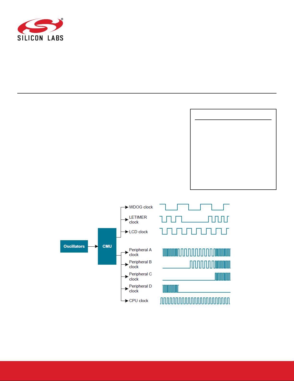
Clock Management Unit (CMU)
This application note provides an overview of the CMU module for EFR32 Wireless
Gecko Series 2 devices with explanations on how to choose clock sources, prescaling,
and clock calibration.
contains information about how to handle oscillators on wake up, external clock
It also
sources, and RC oscillator calibration.
KEY POINTS
• The CMU has several internal clock
sources available.
• The CMU can also use external high
frequency and low frequency clock
sources. Selecting the right clock source is
key for creating low energy applications.
•
This application note includes:
• This PDF document
• Source files
• Example C-code
• Multiple IDE projects
silabs.com | Building a more connected world. Rev. 1.0
Page 2

AN0004.2: EFR32 Series 2 Wireless MCU Clock Management Unit (CMU)
1. Device Compatibility
This application note supports multiple device families, and some functionality is different depending on the device.
EFR32 Wireless Gecko Series 2 consists of the following:
•
EFR32BG21
• EFR32MG21
• EFR32BG22
• EFR32MG22
Device Compatibility
silabs.com | Building a more connected world. Rev. 1.0 | 2
Page 3

AN0004.2: EFR32 Series 2 Wireless MCU Clock Management Unit (CMU)
Functional Description
2. Functional Description
The Clock Management Unit (CMU) controls the oscillators and clocks. It can select the sources for any of the clock branches, additionally some clock branches can be prescaled. The CMU can also enable, disable, or configure the available oscillators.
silabs.com | Building a more connected world. Rev. 1.0 | 3
Page 4

2.1 Clock Branches
AN0004.2: EFR32 Series 2 Wireless MCU Clock Management Unit (CMU)
Functional Description
The CMU
main and sub clock branches are described in the tables below. Some peripherals have dedicated pre-scalers, such as the
LETIMER and TIMERs. A detailed clock tree diagram can be found in the CMU chapter at the beginning of the Functional Description
section of a given device's reference manual.
Table 2.1. Wireless Gecko EFR32xG21 Clock Branches
Main Clock
Branch
1
Clock Source
SYSCLK • HFRCODPLL
•
HFXO
•
FSRCO
• CLKIN0
2
Sub-clock Branch
1
1
• HCLK
•
EXPCLK
Sub-clock Branch
1
2
• PCLK
• CORTEX(CORE)
• GPCRC
Sub-clock Branch
1
3
• LSPCLK
•
I2C1
• USARTn
Sub-clock Branch
1
4
• I2C0
• GPIO
• LDMA
• LE
• PRS
HCLKRADIO • HFXO
EM01GRPACLK • FSCRO
• HFRCODPLL
•
CLKIN
EM23GRPACLK • LFRCO
• LFXO
•
ULFRCO
EM4GRPACLK • LFRCO
• LFXO
•
ULFRCO
IADCCLK • EM01GRPACLK
• HFRCOEM23
•
FSCRO
TRACECLK • HFRCOEM23
• PCLK
•
HCLK
WDOGCLK • LFRCO
• LFXO
•
ULFRCO
• HCLKDIV1024
F
(DPLL) • HFXO
ref
•
CLKIN0
LFXO
•
Note:
1. Not all main and sub clock branches are available on a given device. Refer to the device reference manual and data sheet for
details.
2.
Not all clock sources for main clock branches are available on a given device. Refer to the device reference manual and data
sheet for details.
silabs.com | Building a more connected world. Rev. 1.0 | 4
Page 5

AN0004.2: EFR32 Series 2 Wireless MCU Clock Management Unit (CMU)
Table 2.2. Wireless Gecko EFR32xG22 Clock Branches
Functional Description
Main Clock
Branch
1
Clock Source
2
SYSCLK • HFRCODPLL
•
HFXO
•
FSRCO
• CLKIN0
RHCLK • SYSCLK
EM01GRPACLK • FSCRO
• HFRCODPLL
•
CLKIN
EM23GRPACLK • LFRCO
• LFXO
•
ULFRCO
EM4GRPACLK • LFRCO
• LFXO
•
ULFRCO
Sub-clock Branch
1
2
• HCLK
•
EXPCLK
Sub-clock Branch
1
3
• PCLK
• CORTEX(CORE)
• GPCRC
• GPIO
• LDMA
• LE
• PRS
Sub-clock Branch
1
4
• LSPCLK
•
I2C1
• USARTn
Sub-clock Branch
1
5
• I2C0
IADCCLK • EM01GRPACLK
• FSCRO
TRACECLK •
SYSCLK
WDOGCLK • LFRCO
LFXO
•
•
ULFRCO
• HCLKDIV1024
RTCCCLK • LFXO
•
LFRCO
ULFRCO
•
PRORTCCLK • LFXO
• LFRCO
•
ULFRCO
DPLLREFCLK • HFXO
• CLKIN0
•
LFXO
Note:
1. Not all main and sub clock branches are available on a given device. Refer to the device reference manual and data sheet for
details.
2.
Not all clock sources for main clock branches are available on a given device. Refer to the device reference manual and data
sheet for details.
silabs.com | Building a more connected world. Rev. 1.0 | 5
Page 6

2.2 Clock Sources
AN0004.2: EFR32 Series 2 Wireless MCU Clock Management Unit (CMU)
Functional Description
There are
a maximum of seven oscillators that can be used as clock sources for different purposes. The SYSCLK is usually clocked by
the HFXO, FSRCO or HFRCO, whereas low energy peripherals are usually clocked by the LFXO, LFRCO, or ULFRCO. The
HFRCOEM231 is typically used for the low energy peripherals such as LETIMER.
Table 2.3. Clock Sources
Oscillator Frequency Range
HFXO 38–40 MHz
HFRCODPLL 1–80 MHz
HFRCOEM23
1
1–38 MHz
FSRCO 20 MHz
LFXO 32768 Hz
LFRCO 32768 Hz
ULFRCO 1000 Hz
Note:
1. HFRCOEM23 not available on Wireless Gecko EFR32xG22 devices
select the clock source for a branch (e.g., SYSCLK, EM23GRPACLK), the chosen oscillator must be enabled before it is selected as
To
the clock source. If not done, the modules running from that clock branch will stop. In the case of selecting a disabled oscillator for the
SYSCLK branch, the CPU will stop and can only be recovered after a reset.
After a reset, the SYSCLK branch is clocked by the FSRCO at 20 MHz and all low frequency branches are disabled.
Emlib has functions to enable or disable an oscillator and select it as a clock source.
Table 2.4. emlib Functions for Oscillator Enable, Disable, and Selection
emlib Function Usage Example
CMU_HFXOInit(const CMU_HFXOInit_TypeDef
*hfxoInit)
CMU_LFXOInit(const CMU_LFXOInit_TypeDef
*lfxoInit)
CMU_ClockSelectSet(CMU_Clock_ TypeDef clock,
CMU_Select_TypeDef ref)
• Initializes HFXO Initialize HFXO with parameters specified
by hfxoInit struct
CMU_HFXOInit(&hfxoInit)
• Initializes LFXO Initialize LFXO with parameters specified
by lfxoInit struct
CMU_LFXOInit(&lfxoInit)
• Enables the chosen clock
source in case it has not
been enabled yet.
•
The clock parameter is one of
the main clock branches, and
the ref parameter is one of
the clock sources for the se-
Select HFXO as the source of HFCLK:
CMU_ClockSelectSet (cmuClock_HF,
cmuSelect_HFXO);
Select LFXO as the source of LFACLK:
CMU_ClockSelectSet(cmuClock_LFA,
cmuSelect_LFXO);
lected clock branch.
2.2.1 Clock Input from a Pin
possible to configure the CMU to use an external clock input on the CLKIN0 pin. This clock can be selected as the SYSCLK and as
It is
the DPLL reference using the CMU_SYSCLKCTRL and CMU_DPLLEFCLKCTRL registers, respectively. The input port and pin must
be selected in the GPIO_CMU_CLKIN0ROUTE register by setting the PORT and PIN bits appropriately.
silabs.com | Building a more connected world. Rev. 1.0 | 6
Page 7

2.3 Oscillator Configuration
2.3.1 HFXO
AN0004.2: EFR32 Series 2 Wireless MCU Clock Management Unit (CMU)
Functional Description
The High
Frequency Crystal Oscillator (HFXO) is configured to ensure safe startup and operation for most common crystals by default.
In order to optimize startup time and power consumption for a given crystal, it is possible to adjust certain oscillator parameters. For
more information, refer to application note, AN0016.2: Oscillator Design Considerations.
The HFXO (38 MHz–40 MHz) needs to be configured to ensure safe startup for the given crystal. The HFXO includes on-chip tunable
capacitance, which can replace external load capacitors.
Upon enabling the HFXO, a hardware state machine sequentially applies the configurable startup state, intermediate and steady state
control settings from the HFXO_XTALCFG register. Please refer to the device reference manual for the detailed CMU HFXO control
state machine flow.
Each of the startup state, intermediate startup state and the steady state of the HFXO require configuration. After reaching the steady
operating state, the HFXO configuration can optionally be further tuned to minimize noise and current consumption.
The core bias optimization algorithm can be used to trade off noise and current consumption. It is highly recommended to perform the
optimization once steady state is reached and any time the temperature varies by more than 40 ºC. The optimization is performed by
writing to the COREBIASOPT bitfield of the HFXO_CMD register.
The HFXO configuration can be locked by writing any value other than the UNLOCK code 22542(0x580E) to the LOCKKEY bit field in
the HFXO_LOCK register. To unlock the configuration, write the UNLOCK code to the LOCKKEY bitfield.
Table 2.5. HFXO Configuration
Configuration and Optimization Bit Field and Register
Configurable startup state Bit fields in HFXO_XTALCFG
Configurable intermediate startup state Bit fields in HFXO_XTALCFG
Configurable Steady State Bit fields in HFXO_CTRL
Optimization COREBIASOPT bit field in HFXO_CMD
silabs.com | Building a more connected world. Rev. 1.0 | 7
Page 8

AN0004.2: EFR32 Series 2 Wireless MCU Clock Management Unit (CMU)
Functional Description
2.3.1.1 Using emlib for HFXO Configuration
typedef struct {
CMU_HfxoCbLsbTimeout_TypeDef timeoutCbLsb; /**< Core bias change timeout. */
CMU_HfxoSteadyStateTimeout_TypeDef timeoutSteadyFirstLock; /**< Steady state timeout duration for first lock. */
CMU_HfxoSteadyStateTimeout_TypeDef timeoutSteady; /**< Steady state timeout duration. */
uint8_t ctuneXoStartup; /**< XO pin startup tuning capacitance. */
uint8_t ctuneXiStartup; /**< XI pin startup tuning capacitance. */
uint8_t coreBiasStartup; /**< Core bias startup current. */
uint8_t imCoreBiasStartup; /**< Core bias intermediate startup current. */
CMU_HfxoCoreDegen_TypeDef coreDegenAna; /**< Core degeneration control. */
CMU_HfxoCtuneFixCap_TypeDef ctuneFixAna; /**< Fixed tuning capacitance on XI/XO. */
uint8_t ctuneXoAna; /**< Tuning capacitance on XO. */
uint8_t ctuneXiAna; /**< Tuning capacitance on XI. */
uint8_t coreBiasAna; /**< Core bias current. */
bool enXiDcBiasAna; /**< Enable XI internal DC bias. */
CMU_HfxoOscMode_TypeDef mode; /**< Oscillator mode. */
bool forceXo2GndAna; /**< Force XO pin to ground. */
bool forceXi2GndAna; /**< Force XI pin to ground. */
bool disOnDemand; /**< Disable on-demand requests. */
bool forceEn; /**< Force oscillator enable. */
bool regLock; /**< Lock register access. */
} CMU_HFXOInit_TypeDef;
Emlib has
structures and functions that simplify configuration of the HFXO for efficient operation. Use of emlib is strongly recommended
for this reason and also in order to avoid or workaround errata related to the HFXO.
Initialization of the HFXO depends on the structure of type CMU_HFXOInit_TypeDef:
Structure members can be set by the user, otherwise the default structures CMU_HFXOINIT_DEFAULT and
CMU_HFXOINIT_EXTERNAL_CLOCK can be used as templates for HFXO initialization.
#define CMU_HFXOINIT_DEFAULT \
{ \
cmuHfxoCbLsbTimeout_416us, \
cmuHfxoSteadyStateTimeout_833us, /* First lock */ \
cmuHfxoSteadyStateTimeout_83us, /* Subsequent locks */ \
0U, /* ctuneXoStartup */ \
0U, /* ctuneXiStartup */ \
32U, /* coreBiasStartup */ \
32U, /* imCoreBiasStartup */ \
cmuHfxoCoreDegen_None, \
cmuHfxoCtuneFixCap_Both, \
_HFXO_XTALCTRL_CTUNEXOANA_DEFAULT, /* ctuneXoAna */ \
_HFXO_XTALCTRL_CTUNEXIANA_DEFAULT, /* ctuneXiAna */ \
60U, /* coreBiasAna */ \
false, /* enXiDcBiasAna */ \
cmuHfxoOscMode_Crystal, \
false, /* forceXo2GndAna */ \
false, /* forceXi2GndAna */ \
false, /* DisOndemand */ \
false, /* ForceEn */ \
false /* Lock registers */ \
}
#define CMU_HFXOINIT_EXTERNAL_SINE \
{ \
(CMU_HfxoCbLsbTimeout_TypeDef)0, /* timeoutCbLsb */ \
(CMU_HfxoSteadyStateTimeout_TypeDef)0, /* timeoutSteady, first lock */ \
(CMU_HfxoSteadyStateTimeout_TypeDef)0, /* timeoutSteady, subseq. locks */ \
0U, /* ctuneXoStartup */ \
0U, /* ctuneXiStartup */ \
0U, /* coreBiasStartup */ \
0U, /* imCoreBiasStartup */ \
cmuHfxoCoreDegen_None, \
cmuHfxoCtuneFixCap_None, \
0U, /* ctuneXoAna */ \
0U, /* ctuneXiAna */ \
0U, /* coreBiasAna */ \
false, /* enXiDcBiasAna, false=DC true=AC coupling of signal */ \
cmuHfxoOscMode_ExternalSine, \
false, /* forceXo2GndAna */ \
silabs.com | Building a more connected world. Rev. 1.0 | 8
Page 9

AN0004.2: EFR32 Series 2 Wireless MCU Clock Management Unit (CMU)
false, /* forceXi2GndAna */ \
false, /* DisOndemand */ \
false, /* ForceEn */ \
false /* Lock registers */ \
}
Functional Description
The HFXO
initialization structure is used as an argument when calling the CMU_HFXOInit(const CMU_HFXOInit_TypeDef *hfxoInit)
function, which writes the HFXO initialization parameters to the relevant CMU registers. After calling this function call, the HFXO can be
enabled and selected as the source of HFCLK as shown below:
/* Initialize HFXO with specific parameters */
CMU_HFXOInit_TypeDef hfxoInit = CMU_HFXOINIT_DEFAULT;
CMU_HFXOInit(&hfxoInit);
/* Enable and set HFXO for SYSCLK */
CMU_ClockSelectSet(cmuClock_SYSCLK, cmuSelect_HFXO);
2.3.2 LFXO
The Low
Frequency Crystal Oscillator (LFXO) is configured to ensure safe startup and operation for most common crystals by default.
In order to optimize startup time and power consumption for a given crystal, it is possible to adjust certain oscillator parameters. For
more information, refer to application note, AN0016.2: Oscillator Design Considerations.
The LFXO includes on-chip tunable capacitance, which can replace external load capacitors. The LFXO is configured by bit fields in the
LFXO_CTRL, LFXO_CFG and LXFO_CAL registers. Note that these bit fields should set only during initialization and are not be
changed while the LFXO is enabled. The LXFO configuration can be locked by writing any value other than the UNLOCK code 6688
(0x1A20) to the LOCKKEY bit field in the LFXO_LOCK register. To unlock the configuration write the UNLOCK code to the LOCKKEY
bitfield.
The LFXO_CFG register can only be written when the LFXO is in FORCEOFF mode otherwise the write will be blocked and a bus fault
occurs. In order to avoid the bus fault, wait for the ENS bit in the LFXO_STATUS register to clear before modifying LFXO_CFG. The
LFXO_CAL register can be modified only when the CALBUSY in the LFXO_SYNCBUSY register is low, otherwise the write will be
blocked and a busfault will be triggered.
Table 2.6. LFXO Registers for LFXO Configuration
Bit Field Register Usage
GAIN LFXO_CAL Adjusts the oscillator startup gain .
CAPTUNE LFXO_CAL Tunes the internal load capacitance connected between X_P and ground and X_N and ground
symmetrically.
FAILDETEM4UEN LFXO_CTRL Set this bit to enable EM4 exit on failure detection.
FAILDETEN LFXO_CTRL Set this bit to enable oscillator failure detection.
DISONDEMAND LFXO_CTRL Set this bit to disable on demand requests from hardware.
FORCEN LFXO_CTRL Set this bit to force the oscillator to be enabled regardless of on demand requests
TIMEOUT LFXO_CFG Sets the startup delay for the LFXO. Minimum 256 cycles for crystals.
HIGHAMPL LFXO_CFG Setting this bit drives the crystal with a higher amplitude waveform, which in turn provides safer
operation, somewhat improves duty cycle, and lowers sensitivity to noise at the cost of increased
current consumption.
AGC LFXO_CFG Setting this bit enables Automatic Gain Control, which limits the amplitude of the driving waveform
in order to reduce current draw. When AGC is disabled, the LFXO runs at the startup current, and
the crystal will oscillate rail to rail, providing safer operation, improved duty cycle, and lower sensitivity to noise at the cost of increased current consumption.
MODE LFXO_CFG Determines whether the LFXO uses a crystal or sine wave as its source.
silabs.com | Building a more connected world. Rev. 1.0 | 9
Page 10

2.3.2.1 Using emlib for LFXO Configuration
AN0004.2: EFR32 Series 2 Wireless MCU Clock Management Unit (CMU)
Functional Description
emlib has
structures and functions that simplify configuration of the LFXO for efficient operation. Use of emlib is strongly recommended
for this reason and also in order to avoid or workaround errata related to the LFXO.
Initialization of the HFXO depends on the structure of type CMU_LFXOInit_TypeDef:
typedef struct {
uint8_t gain; /**< Startup gain. */
uint8_t capTune; /**< Internal capacitance tuning. */
CMU_LfxoStartupDelay_TypeDef timeout; /**< Startup delay. */
CMU_LfxoOscMode_TypeDef mode; /**< Oscillator mode. */
bool highAmplitudeEn; /**< High amplitude enable. */
bool agcEn; /**< AGC enable. */
bool failDetEM4WUEn; /**< EM4 wakeup on failure enable. */
bool failDetEn; /**< Oscillator failure detection enable. */
bool disOnDemand; /**< Disable on-demand requests. */
bool forceEn; /**< Force oscillator enable. */
bool regLock; /**< Lock register access. */
} CMU_LFXOInit_TypeDef;
Structure members
CMU_LFXOINIT_EXTERNAL_CLOCK can be used as templates for LFXO initialization.
#define CMU_LFXOINIT_DEFAULT \
{ \
1, \
38, \
cmuLfxoStartupDelay_4KCycles, \
cmuLfxoOscMode_Crystal, \
false, /* highAmplitudeEn */ \
true, /* agcEn */ \
false, /* failDetEM4WUEn */ \
false, /* failDetEn */ \
false, /* DisOndemand */ \
false, /* ForceEn */ \
false /* Lock registers */ \
}
can be set by the user, otherwise the default structures CMU_LFXOINIT_DEFAULT and
The LFXO
initialization structure is used as an argument when calling the CMU_LFXOInit(const CMU_LFXOInit_TypeDef *lfxoInit)
function, which writes the HFXO initialization parameters to the relevant CMU registers. After calling this function call, the HFXO can be
enabled and selected as the source of HFCLK as shown below:
// Initialize LFXO
CMU_LFXOInit_TypeDef lfxoInit = BSP_CLK_LFXO_INIT;
lfxoInit.forceEn=true;
CMU_LFXOInit(&lfxoInit);
silabs.com | Building a more connected world. Rev. 1.0 | 10
Page 11

2.3.3 HFRCODPLL, HFRCOEM23
AN0004.2: EFR32 Series 2 Wireless MCU Clock Management Unit (CMU)
Functional Description
The HFRCO
defaults to operation in the 19 MHz band but can be switched to operate in one of the other preset frequency bands by
changing the FREQRANGE bit field in the HFRCO_CAL. The HFRCO has 3 modes: forced off, forced on and On-Demand. These
modes are controlled by the bit fields in the HFRCO_CTRL register.
Table 2.7. High Frequency RC Oscillator Band Selection
Oscillator Frequency Band
HFRCODPLL • 1 MHz (DIV4 from 4 MHz)
•
2 MHz (DIV2 from 4 MHz)
4 MHz
•
• 7 MHz
• 13 MHz
• 16 MHz
• 19 MHz
• 26 MHz
• 32 MHz
• 38 MHz
• 48 MHz
• 56 MHz
• 64 MHz
• 80 MHz
HFRCOEM23
1
• 1 MHz (DIV4 from 4 MHz)
•
2 MHz (DIV2 from 4 MHz)
•
4 MHz
• 13 MHz
• 16 MHz
• 19 MHz
• 26 MHz
• 32 MHz
• 40 MHz
Note:
1. HFRCOEM23 not available on Wireless Gecko EFR32xG22 devices
specific values that select each tuning band are written to the TUNING bit field in the HFRCO_CAL register. Each band is calibra-
The
ted during production, with suitable tuning values written to the Device Information (DI) page.
The HFRCO frequency can be more accurately tuned at the cost of increased current consumption via the FINETUNING bit field in the
HFRCO_CAL register.
The HFRCO configuration can be locked by writing any value other than the UNLOCK code 33173 (0x8195) to the LOCKKEY bit field in
the HFRCO_LOCK register. To unlock the configuration write the UNLOCK code to the LOCKKEY bitfield.
Emlib has specific functions to change the frequency band to which the HFRCODPLL and HFRCOEM23 are tuned. Use of emlib is
strongly recommended because it specifically handles the need to increase the number of flash wait states when a higher frequency
tuning band is selected. These functions switch to the desired frequency band by loading the correct tuning value from the Device Information (DI) page.
silabs.com | Building a more connected world. Rev. 1.0 | 11
Page 12

AN0004.2: EFR32 Series 2 Wireless MCU Clock Management Unit (CMU)
Table 2.8. emlib Functions for Changing the HFRCO Tuning Band
emlib Function Usage Example
Functional Description
CMU_HFRCODPLLBandSet(CMU_HFRCOFreq_
TypeDef setFreq)
CMU_HFRCOEM23BandSet(CMU_HFRCOFreq_
TypeDef setFreq)
Change HFRCO frequency band. CMU_HFRCODPLLBandSet(
cmuHFRCOEM23Freq_40M0Hz);
Change HFRCO frequency band. CMU_HFRCOEM23BandSet(
cmuHFRCOEM23Freq_2M0Hz);
2.3.4 LFRCO
It
possible to calibrate the LFRCO to achieve higher accuracy. The frequency is adjusted by changing the FREQTRIM bitfield in the
is
LFRCO_CAL register. The LFRCO is also calibrated in production, and its default FREQTRIM value is set during reset.
The LFRCO is part of the on-demand architecture and can be requested by the CMU whenever it is needed.
The LFRCO configuration can be locked by writing any value other than the UNLOCK code 9731 (0x2603) to the LOCKKEY bit field in
the LFRCO_LOCK register. To unlock the configuration write the UNLOCK code to the LOCKKEY bitfield.
2.3.5 FSRCO
The FSRCO is a 20 MHz fixed frequency RC oscillator that can start and stop very quickly. There are no configuration or status registers associated with this oscillator, it is enabled by selecting it as the clock source. This is the default oscillator and provides SYSCLK
upon reset. This oscillator is available in all energy modes.
2.3.6 ULFRCO
The ULFRCO is always on in EM0, EM1, EM2, EM3 and EM4 and does not have any configurable settings. As such, it is always available as a clock source for many of the peripherals in the low-frequency clock domains. It is not possible to calibrate the ULFRCO to
achieve higher accuracy.
2.4 Oscillator Start-Up Time and Time-Out
The start-up time for each of the previously discussed oscillators differs and, in certain cases, can be further extended by one or more
programmable time-out delays. When enabled, the oscillator's output is given time to stabilize by stalling assertion of its ready signal for
the specified number of clock cycles. Low start-up times can be selected when the clock is coming from a high quality source, while
longer time-out delays are necessary when the clock is coming directly from a crystal.
Programmable time-outs are available for the LFXO and HFXO. The LFRCO, HFRCODPLL, HFRCOEM23, ULFRCO, and FSRCO
timeout delays are fixed and cannot be changed.
Table 2.9. Oscillator Time-Out Configuration
Oscillator Bit Field Register
LFXO TIMEOUT LFXO_CFG
HFXO • TIMEOUTCBLSB
HFXO_XTALCFG
• TIMEOUTSTEADY
LFRCO Start-up time is fixed.
HFRCO(DPLL and EM23) Start-up time is fixed.
FSRCO Start-up time is fixed.
ULFRCO Start-up time is fixed.
silabs.com | Building a more connected world. Rev. 1.0 | 12
Page 13

2.5 Prescaling
AN0004.2: EFR32 Series 2 Wireless MCU Clock Management Unit (CMU)
Functional Description
Each of
the clock sub-branches derived from the system clock, SYSCLK, can be individually prescaled. SYSCLK is divided by 1/2/4 to
derive the AHB clock, HCLK, which in turn is divided by 1 or 2 to derive the APB clock, PCLK, which is divided by 1 or 2 to derive the
low speed APB clock, LSPCLK.
Prescaling may be controlled independently by dedicated bit fields for peripherals, such as LETIMER, in the low frequency clock domains (EM23GRPACLK, EM4GRPACLK).
Table 2.10. Prescaler of Clock Branches
Clock Branch
Prescaler Bitfield
1
Prescaler Register Prescaler Range
HCLK HCLKPRESC CMU_SYSCLKCTRL 1 to 4
PCLK PCLKPRESC CMU_SYSCLKCTRL 1 to 2
LSPCLK - - 2
HCLKRADIO - - 1
EM01GRPACLK - - 1
EM23GRPACLK - - 1
EM4GRPACLK - - 1
IADCCLK - - 1
TRACECLK - - 1
WDOGCLK - - 1
Note:
1. Not all prescaler bitfields are available on a given device. Refer to the device reference manual and data sheet for details.
Emlib has a function to set the clock divisors, and its use is highly encouraged because flash waitstates are handled by this function.
Table 2.11. emlib Clock Divisor Functions
emlib Function Divider/Prescaler Example
CMU_ClockDivSet(CMU_Clock_TypeDef
clock, CMU_ClkDiv_TypeDef div)
One of the enumerated power-of-2 dividers
of type CMU_ClkDiv_TypeDef
Divide by 4 for HCLK:
CMU_ClockDivSet(cmuClock_HCLK,
cmuClkDiv_4);
When using these functions, careful consideration is required for both parameters. Not all clocks have a divisor, and the maximum divisor value is also not the same for the different clocks (HCLK, for instance, has a maximum of 4 while the PCLK can only be divided by 1
or 2).
silabs.com | Building a more connected world. Rev. 1.0 | 13
Page 14
2.6 Flash Wait States
AN0004.2: EFR32 Series 2 Wireless MCU Clock Management Unit (CMU)
Functional Description
When increasing
the memory subsystem clock (HCLK) frequency above certain limits, the number of wait states required for flash read
accesses must be increased before the frequency change is performed. Likewise, the number of wait states can be reduced when the
HFCLK frequency falls below certain limits, and this must be performed after the frequency change has taken place. Wait state and
frequency changes are properly sequenced and handled automatically by emlib's CMU functions, and their use is strongly encouraged.
Changes to the number of wait states can be made under user control directly by writing to the MODE bit field in the MSC_READCTRL
register. It is recommended to use the CMU_UpdateWaitStates() API to set the waitstates, freq is the core clock frequency and the
vscale parameter is ignored.
Table 2.12. Flash Wait States for EFR32xG21
Clock Frequency Minimum Flash Wait States
HCLK
< 39 MHz 0
HCLK > 39 MHz 1
Table 2.13. Flash Wait States for EFR32xG22
Clock Frequency Minimum Flash Wait States
HCLK < 40 MHz 0
HCLK > 40 MHz 1
The emlib functions below optimize flash access wait-state configuration if the source or frequency of HFCLK is changed when invoking
these functions.
• CMU_ClockDivSet(CMU_Clock_TypeDef clock, CMU_ClkDiv_TypeDef div)
• CMU_ClockSelectSet(CMU_Clock_TypeDef clock, CMU_Select_TypeDef ref)
• CMU_HFRCODPLLBandSet(CMU_HFRCOFreq_TypeDef setFreq)
• CMU_HFRCOEM23BandSet(CMU_HFRCOFreq_TypeDef setFreq)
• CMU_UpdateWaitStates(uint32_t freq, int vscale)
2.7 External Clock Sources
By
default,
the LFXO and HFXO are started in crystal mode, but it is possible to connect an external clock source. The HFXO can use
an active external sine wave clock source connected to the HFXTAL_I pin. The LFXO can operate from either a digital or sine wave
clock source to the LFXTAL_I pin of the LFXO as discussed in the following sections.
2.7.1 External Sine Wave
An AC-coupled, externally buffered sine wave can be applied to the HFXTAL_I or LFXTAL_I pin. The amplitude of this signal must be at
least 200 mV peak-to-peak, and the frequency is subject to the same limit as that of a crystal connected to the HFXO or LFXO.
Each oscillator has a way to be configured for use with a stimulus other than a crystal. In the case of the HFXO, the MODE bit in the
HFXO_CFG register is set to indicate that an external clock source (EXTCLK) is being used. Sine wave operation for the LFXO is selected by the BUFEXTCLK setting of the LFXO_CFG register's MODE bit field.
2.7.2 Digital External Clock
A rail-to-rail square wave with 50% duty cycle can be applied to the LFXTAL_I pin, subject to the same frequency limit as that of a
crystal connected to the LFXO.
Operation with a digital external clock for the LFXO is selected by the DIGEXTCLK setting of the LFXO_CFG register's MODE bit field.
2.7.3 Oscillator Pin Availability
When a clock is supplied via LFXTAL_I, the corresponding LFXTAL_O pin is not needed and can be used for GPIO or peripheral functionality.
silabs.com | Building a more connected world. Rev. 1.0 | 14
Page 15

2.8 Output Clock to Pin
AN0004.2: EFR32 Series 2 Wireless MCU Clock Management Unit (CMU)
Functional Description
The CMU
can drive user-specified clocks on certain pins. Selection is done using the CLKOUTSELn bit fields in the CMU_EXPORTCLKCTRL register. It is also necessary to (a) select which pins are driven in the GPIO_CMU_CLKOUTnROUTE register, (b) enable the pin in the GPIO_CMU_ROUTEEN register, and (c) configure them as outputs in the appropriate GPIO pin mode registers.
Note that a clock sourced from an oscillator (e.g. the HFXO) can be unstable after startup and should not be output on a pin before its
corresponding ready flag (e.g. HFXORDY) is set in the status register (e.g. HFXO_STATUS).
Table 2.14. Clock Output on a Pin
Pin Bit Field and Registers
CMU_OUT • CLKOUTSEL0 in CMU_EXPORTCLKCTRL
•
ULFRCO
LFRCO
•
• LFXO
• HFXO
• FSRCO
• HFEXPCLK
• HFRCODPLL
• HFRCOEM23
• HCLK
CMU_OUT1 • CLKOUTSEL1 in CMU_EXPORTCLKCTRL
•
ULFRCO (directly from oscillator)
ULFRCO
•
• LFRCO
• LFXO
• HFXO
• FSRCO
• HFEXPCLK
• HFRCODPLL
• HFRCOEM23
• HCLK
CMU_OUT21 • CLKOUTSEL2 in CMU_CTRL
•
ULFRCO
•
LFRCO
• LFXO
• HFXO
• FSRCO
• HFEXPCLK
• HFRCODPLL
• HFRCOEM23
• HCLK
Enable CLKOUT0PEN, CLKOUT1PEN, and CLKOUT2PEN1 in
GPIO_CMU_ROUTEEN register.
Location PORT and PIN bitfields in GPIO_CMU_CLKOUT0ROUTE,
GPIO_CMU_CLKOUT1ROUTE and
GPIO_CMU_CLKOUT2ROUTE
silabs.com | Building a more connected world. Rev. 1.0 | 15
Page 16

AN0004.2: EFR32 Series 2 Wireless MCU Clock Management Unit (CMU)
3. Revision History
Revision 1.0
March, 2020
• Added EFR32MG22 and EFR32BG22 to the supported parts list
• Added Wireless Gecko EFR32xG22 clock tree and flash wait state information
• Added notes throughout that the HFRCOEM23 is not featured on EFR32xG22 devices
• Improved formatting of the clock tree table
• Added Revision History
Revision 0.1
April, 2019
• Initial revision
Revision History
silabs.com | Building a more connected world. Rev. 1.0 | 16
Page 17

Smart.
Connected.
Energy-Friendly.
Products
www.silabs.com/products
Quality
www.silabs.com/quality
Support and Community
community.silabs.com
http://www.silabs.com
Silicon Laboratories Inc.
400 West Cesar Chavez
Austin, TX 78701
USA
Disclaimer
Silicon Labs intends to provide customers with the latest, accurate, and in-depth documentation of all peripherals and modules available for system and software implementers using or
intending to use the Silicon Labs products. Characterization data, available modules and peripherals, memory sizes and memory addresses refer to each specific device, and "Typical"
parameters provided can and do vary in different applications. Application examples described herein are for illustrative purposes only. Silicon Labs reserves the right to make changes without
further notice to the product information, specifications, and descriptions herein, and does not give warranties as to the accuracy or completeness of the included information. Without prior
notification, Silicon Labs may update product firmware during the manufacturing process for security or reliability reasons. Such changes will not alter the specifications or the performance
of the product. Silicon Labs shall have no liability for the consequences of use of the information supplied in this document. This document does not imply or expressly grant any license
to design or fabricate any integrated circuits. The products are not designed or authorized to be used within any FDA Class III devices, applications for which FDA premarket approval is
required, or Life Support Systems without the specific written consent of Silicon Labs. A "Life Support System" is any product or system intended to support or sustain life and/or health,
which, if it fails, can be reasonably expected to result in significant personal injury or death. Silicon Labs products are not designed or authorized for military applications. Silicon Labs
products shall under no circumstances be used in weapons of mass destruction including (but not limited to) nuclear, biological or chemical weapons, or missiles capable of delivering
such weapons. Silicon Labs disclaims all express and implied warranties and shall not be responsible or liable for any injuries or damages related to use of a Silicon Labs product in such
unauthorized applications.
Trademark Information
Silicon Laboratories Inc.®, Silicon Laboratories®, Silicon Labs®, SiLabs® and the Silicon Labs logo®, Bluegiga®, Bluegiga Logo®, ClockBuilder®, CMEMS®, DSPLL®, EFM®, EFM32®,
EFR, Ember®, Energy Micro, Energy Micro logo and combinations thereof, "the world’s most energy friendly microcontrollers", Ember®, EZLink®, EZRadio®, EZRadioPRO®, Gecko®,
Gecko OS, Gecko OS Studio, ISOmodem®, Precision32®, ProSLIC®, Simplicity Studio®, SiPHY®, Telegesis, the Telegesis Logo®, USBXpress® , Zentri, the Zentri logo and Zentri DMS, ZWave®, and others are trademarks or registered trademarks of Silicon Labs. ARM, CORTEX, Cortex-M3 and THUMB are trademarks or registered trademarks of ARM Holdings. Keil is a
registered trademark of ARM Limited. Wi-Fi is a registered trademark of the Wi-Fi Alliance. All other products or brand names mentioned herein are trademarks of their respective holders.
 Loading...