

Page 1
AN0002.1: EFM32 and EFR32 Wireless
Gecko Series 1 Hardware Design
Considerations
This application note details hardware design considerations for
EFM32
and EFR32 Wireless Gecko Series 1 devices. For hardware design considerations for EFM32 and EZR32 Wireless
MCU Series 0 devices, refer to application note AN0002.0:
EFM32 and EZR32 Wireless MCU Series 0 Hardware Design
Considerations.
Topics specifically covered are supported power supply configurations, supply filtering
considerations, debug interface connections, and external clock sources.
For more information on hardware design and layout considerations for the DC-DC
converter on EFM32 and EFR32 Wireless Gecko Series 1 devices, see application
note AN0948: EFM32 and EFR32 Series 1 Power Configurations and DC-DC.
For more information on hardware layout considerations for the radio portion of EFR32
Wireless Gecko Series 1 devices, see application notes AN930.1: EFR32 Series 1 2.4
GHz Matching Guide, AN933.1: EFR32 Series 1 Minimal BOM, and AN928.1: EFR32
Series 1 Layout Design Guide.
KEY POINTS
• Decoupling capacitors are crucial to
ensuring the integrity of the device's power
supplies.
•
The debug interface consists of two
communication pins (SWCLK and
SWDIO).
• External clock sources must be connected
to the device correctly for proper
operation.
silabs.com | Building a more connected world. Rev. 1.55
Page 2

AN0002.1: EFM32 and EFR32 Wireless Gecko Series 1 Hardware Design Considerations
1. Device Compatibility
This application note supports multiple device families, and some functionality is different depending on the device.
Device Compatibility
EFM32 Series 1
• EFM32 Jade Gecko (EFM32JG1/EFM32JG12)
• EFM32 Pearl Gecko (EFM32PG1/EFM32PG12)
• EFM32 Giant Gecko (EFM32GG11/EFM32GG12)
• EFM32 Tiny Gecko (EFM32TG11)
EFR32 Wireless Gecko Series 1 consists of:
• EFR32 Blue Gecko (EFR32BG1/EFR32BG12/EFR32BG13/EFR32BG14)
• EFR32 Flex Gecko (EFR32FG1/EFR32FG12/EFR32FG13/EFR32FG14)
• EFR32 Mighty Gecko (EFR32MG1/EFR32MG12/EFR32MG13/EFR32MG14)
consists of:
silabs.com | Building a more connected world. Rev. 1.55 | 2
Page 3

AN0002.1: EFM32 and EFR32 Wireless Gecko Series 1 Hardware Design Considerations
Power Supply Overview
2. Power Supply Overview
2.1 Introduction
Although the EFM32 and EFR32 Wireless Gecko Series 1 devices have very low average current consumption, proper decoupling is
crucial. As for all digital circuits, current is drawn in short pulses corresponding to the clock edges. Particularly when several I/O lines
are switching simultaneously, transient current pulses on the power supply can be in the order of several hundred mA for a few nanoseconds, even though the average current consumption is quite small.
These kinds of transient currents cannot be properly delivered over high impedance power supply lines without introducing considerable noise in the supply voltage. To reduce this noise, decoupling capacitors are employed to supplement the current during these short
transients.
2.2 Decoupling Capacitors
Decoupling capacitors make the current loop between supply, MCU, and ground as short as possible for high frequency transients.
Therefore, all decoupling capacitors should be placed as close as possible to each of their respective power supply pins, ground pins,
and PCB (Printed Circuit Board) ground planes.
All external decoupling capacitors should have a temperature range reflecting the environment in which the application will be used. For
example, a suitable choice might be X5R ceramic capacitors with a change in capacitance of ±15% over the temperature range -55 to
+85 °C (standard temperature range devices) or -55 to +125 °C (extended temperature range devices).
For regulator output capacitors (DECOUPLE, VREGSW, and VREGO, if available), the system designer should pay particular attention
to the characteristics of the capacitor over temperature and bias voltage. Some capacitors (particularly those in smaller packages or
using cheaper dielectrics) can experience a dramatic reduction in capacitance value across temperature or as the DC bias voltage increases. Any change pushing the regulator output capacitance outside the data sheet specified limits may result in output instability on
that supply.
2.3 Power Supply Requirements
An important consideration for all devices is the voltage requirements and dependencies between the power supply pins. The system
designer needs to ensure that these power supply requirements are met, regardless of power configuration or topology. Please see the
device data sheet for absolute maximum rating and additional details regarding relative system voltage constraints.
EFM32 Series 1 Power Supply Requirements
• VREGVDD = AVDD (Must be the highest voltage in the system)
• VREGVDD ≥ DVDD
• VREGVDD ≥ IOVDD
• DVDD ≥ DECOUPLE
EFR32 Wireless Gecko Series 1 Power Supply Requirements
• VREGVDD = AVDD (Must be the highest voltage in the system)
• VREGVDD ≥ DVDD
• VREGVDD ≥ PAVDD (For 2.4 GHz or dual-band devices, PAVDD refers to the device pin; for sub-GHz devices, PAVDD refers to
the external power amplifier supply)
• VREGVDD ≥ RFVDD
• VREGVDD ≥ IOVDD
• DVDD ≥ DECOUPLE
silabs.com | Building a more connected world. Rev. 1.55 | 3
Page 4
AN0002.1: EFM32 and EFR32 Wireless Gecko Series 1 Hardware Design Considerations
Power Supply Overview
Power Supply Pin Overview
Note that not all supply pins exist on all devices. The table below provides an overview of the available power supply pins.
Table 2.1. Power Supply Pin Overview
Pin Name Product Family Description
AVDD All devices Supply to analog peripherals
DECOUPLE All devices Output of the internal digital LDO
IOVDD All devices GPIO supply voltage
VBUS All USB-enabled devices Primary input to the internal 3.3 V LDO, and the USB 5 V sense
input. Can be connected to the USB 5 V supply. If unused, may
be left floating (a weak internal pull-down will ensure the pin remains at ground).
VREGI All USB-enabled devices Secondary input to the internal 3.3 V LDO. Typically connected
to the USB 5 V supply. If usused, may be left floating (a weak
internal pull-down will ensure the pin remains at ground).
VREGO All USB-enabled devices Output of the internal 3.3 V LDO
VREGVDD All devices Input to the DC-DC converter
VREGSW All devices DC-DC powertrain switching node
VREGVSS All devices DC-DC ground
DVDD All devices DC-DC feedback node and input to the internal digital LDO
RFVDD EFR32 Wireless Gecko Series 1 only Supply to radio analog and HFXO
PAVDD EFR32 Wireless Gecko Series 1 only Supply to 2.4 GHz radio power amplifier
2.4 DECOUPLE
All
EFM32 and EFR32 Wireless Gecko Series 1 devices include an internal linear regulator that powers the core and digital logic. The
DECOUPLE pin is the the output of the digital LDO, and requires a 1 µF capacitor.
EFM32xG1 and EFR32xG1 DECOUPLE Pin
On EFM32xG1 and EFR32xG1 devices, the input supply to the digital LDO is the DVDD pin, and the DECOUPLE pin is the output of
the LDO.
V
Main
Supply
DD
+
–
C
DVDD1
0.1 µF
DVDD
Digital
LDO
DECOUPLE
C
DE
C
1 µF
Digital
Logic
Figure 2.1. DVDD and DECOUPLE on EFM32xG1 and EFR32xG1 devices
silabs.com | Building a more connected world. Rev. 1.55 | 4
Page 5
EFM32xG11/12 and EFR32xG12/13/14 DECOUPLE Pin
AN0002.1: EFM32 and EFR32 Wireless Gecko Series 1 Hardware Design Considerations
Power Supply Overview
On EFM32xG11/12
DVDD pin. The DECOUPLE pin the output of the LDO. Note that while supplied from the AVDD pin, the digital LDO current is limited to
20 mA. After start up, firmware should configure EMU_PWRCTRL_REGPWRSEL to power the digital LDO from DVDD.
2.5 IOVDD
IOVDD pin(s) provide decoupling for all of the GPIO pins on the device. A 0.1 µF capacitor per IOVDD pin is recommend, along
The
with a 10 µF bulk capacitor. The bulk capacitor value may safely be reduced if there are other large bulk capacitors on the same supply
(e.g., if IOVDD = AVDD = system main supply, and the main supply already has multiple 10 µF).
and EFR32xG12/13/14 devices, the input supply to the digital LDO is either the AVDD pin (power on default) or the
AVDD
V
DD
Main
Supply
Figure 2.2. DVDD and DECOUPLE on EFM32xG11/12 and EFR32xG12/13/14 devices
+
–
C
0.1 µF
DVDD1
C
DE
1 µF
DVDD
DVDD
REGPWRSEL
DECOUPLE
C
01
Digital
LDO
Digital
Logic
V
Main
Supply
DD
+
–
C
VDD_n
IO
0.1 µF
IOVDD_n
. . .
IOVDD_0
C
IOVDD
10 µF
Figure 2.3. IOVDD Decoupling
Note: IOVDD
DC converter defaults to an unconfigured safe state with its output floating such that connected circuits remain unpowered until firmware performs the necessary configuration. Fresh from the factory, a blank device will run the bootloader and fail in its attempt to communicate with a host via the BOOT_RX and BOOT_TX pins without IOVDD power. Use of the debug interface (DBG_SWCLKTCK and
DBG_SWDIOTMS) for initial firmware download would, in this case, be similarly fruitless.
should not be supplied from the DC-DC converter on EFM32xG11/12 and EFR32xG12/13/14 devices. At reset, the DC-
C
VDD_0
IO
0.1 µF
silabs.com | Building a more connected world. Rev. 1.55 | 5
Page 6
AN0002.1: EFM32 and EFR32 Wireless Gecko Series 1 Hardware Design Considerations
Power Supply Overview
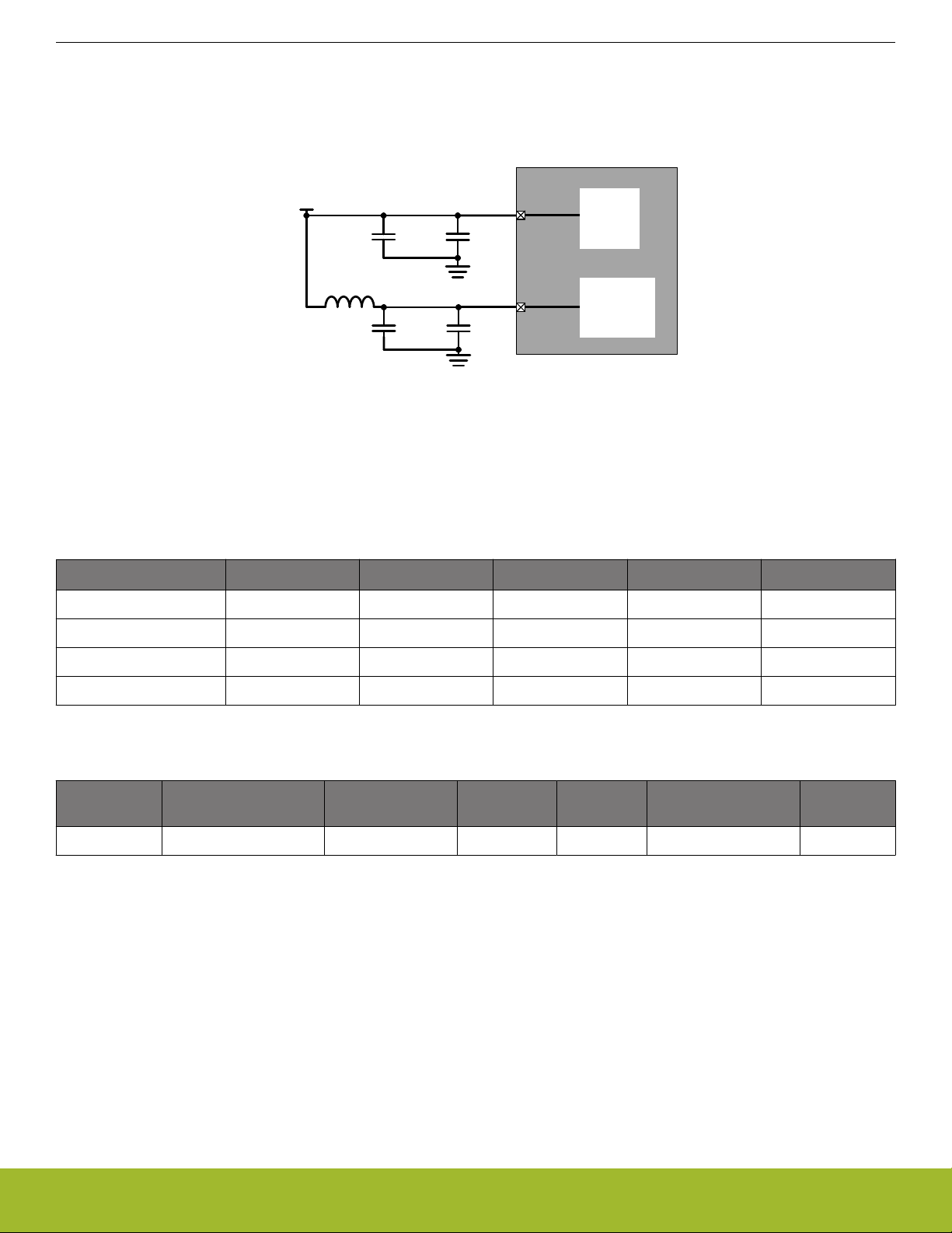
2.6 AVDD
analog peripheral performance of the device is impacted by the quality of the AVDD power supply. For applications with less de-
The
manding analog performance, a simpler decoupling scheme for AVDD may be acceptable. For applications requiring the highest quality
analog performance, more robust decoupling and filtering is required.
Note that the number of AVDD analog power pins may vary by device and package.
2.6.1 AVDD Standard Decoupling
The figure below illustrates a standard approach for decoupling the AVDD pin(s). In general, one 10 µF bulk capacitor (C
as one 10 nF capacitor for each AVDD pin (C
Main
Supply
AVDD_0
through C
V
DD
+
–
), must be provided.
AVDD_n
C
10 nF
VDD_n
A
AVDD_n
. . .
AVDD
AVDD_0
C
VDD
A
10 µF
Figure 2.4. AVDD Standard Decoupling
2.6.2 AVDD Improved Decoupling
figure below illustrates an improved approach for decoupling and filtering the AVDD pin(s). In general, one 10 µF bulk capacitor
The
(C
), as well as one 10 nF capacitor for each AVDD pin (C
AVDD
and series 1 Ω resistor provide additional power supply filtering and isolation.
AVDD_0
C
VDD_0
A
10 nF
through C
), must be provided. In addition, a ferrite bead
AVDD_n
), as well
Main
Supply
V
DD
+
–
FB
VDD
R
AVDD
1 Ω
C
A
VDD_n
10 nF
AVDD_n
. . .
AVDD_0
C
VDD
A
10 µF
Figure 2.5. AVDD Improved Decoupling
silabs.com | Building a more connected world. Rev. 1.55 | 6
C
VDD_0
A
10 nF
Page 7
AN0002.1: EFM32 and EFR32 Wireless Gecko Series 1 Hardware Design Considerations
The table below lists some recommended ferrite bead part numbers suitable for AVDD filtering.
Table 2.2. Recommended Ferrite Beads
Power Supply Overview
Manufacturer Part Number Impedance I
(mA) DCR (Ω) Operating Tem-
MAX
Package
perature (°C)
Würth Electronics 74279266 1 kΩ @ 100 MHz 200 0.600 -55 to +125 0603/1608
Murata BLM21BD102SN1D 1 kΩ @ 100 MHz 200 0.400 -55 to +125 0805/2012
2.7 USB (VREGI & VREGO)
Some
EFM32 and EFR32 Wireless Gecko Series 1 devices integrate a USB controller and a 3.3 V LDO. Power supply decoupling, as
well as signalling and control signals, are discussed in Section 6. USB.
2.8 DC-DC
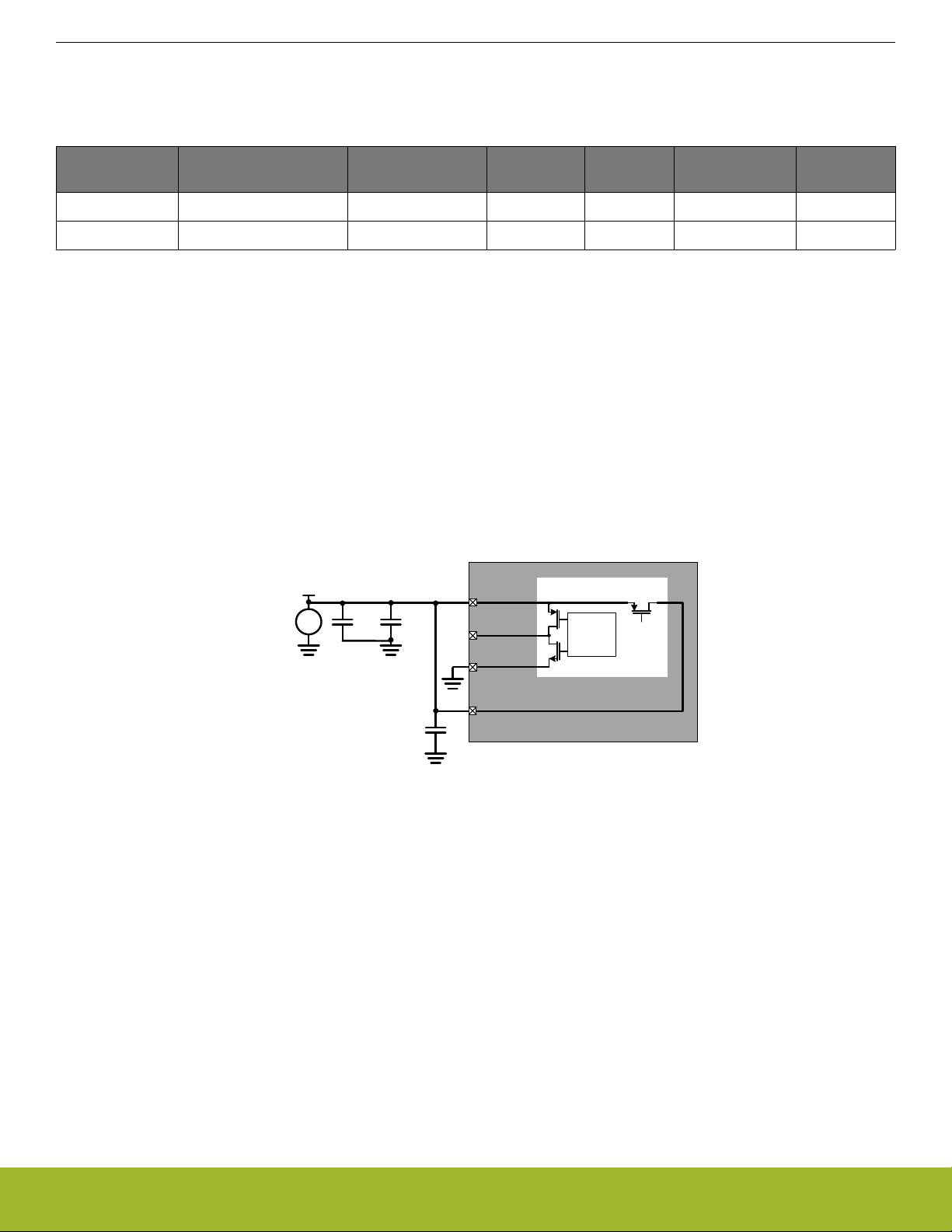
Some EFM32 and EFR32 Wireless Gecko Series 1 devices provide an on-chip DC-DC converter that can be used for improved power
efficiency. However, the additional switching noise present on the DC-DC converter output (V
), necessitates the use of specific
DCDC
filtering components.
2.8.1 DC-DC — Unused
When the DC-DC converter is not used, the DVDD pin should be shorted to the VREGVDD pin. VREGSW must be left floating, and
VREGVSS should be grounded.
Bypass
witch
S
OFF
Main
Supply
V
DD
+
–
C
VDD
10 µF
C
VDD1
0.1 µF
VREGVDD
VREGSW
DC-DC
Driver
VREGVSS
DC-DC
DVDD
C
D
VDD
0.1 µF
Figure 2.6. Configuration when the DC-DC converter is unused
silabs.com | Building a more connected world. Rev. 1.55 | 7
Page 8
AN0002.1: EFM32 and EFR32 Wireless Gecko Series 1 Hardware Design Considerations
Power Supply Overview
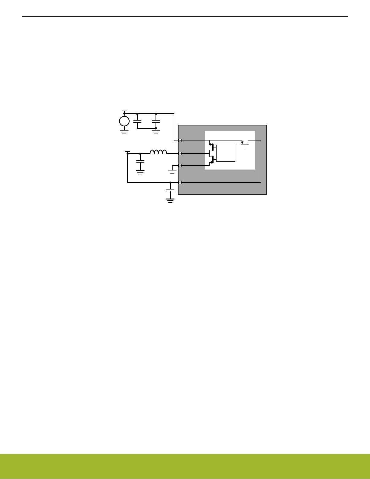
2.8.2 DC-DC — Powering DVDD
the lowest power applications, the DC-DC converter can be used to power the DVDD supply (as well as RFVDD and PAVDD on
For
EFR32 Wireless Gecko Series 1) as shown in the figure below. In this configuration, the DC-DC Output (V
In addition to being the DC-DC converter feedback path, the DVDD pin powers the internal digital LDO, which in turn powers the digital
circuits.
) is connected to DVDD.
DCDC
The system designer should pay particular attention to the characteristics of the DC-DC output capacitor (C
) over temperature and
DCDC
bias voltage. Some capacitors, particularly those in smaller packages or using cheaper dielectrics, can experience a dramatic reduction
in nominal capacitance in response to temperature changes or as the DC bias voltage increases. Any change pushing the DC-DC output capacitance outside the data sheet specified limits may result in output instability on that supply.
V
DD
Main
Supply
V
+
–
DCDC
10 µF
C
VDD
L
DCDC
4.7 µH
C
DCDC
4.7 µF
C
VDD1
0.1 µF
VREGVDD
VREGSW
VREGVSS
DC-DC
Driver
Bypass
witch
S
OFF
DC-DC
DVDD
C
DVDD
0.1 µF
Figure 2.7. DC-DC Converter Powering DVDD
Note: C
mended for new designs due to its improved performance under dynamic load conditions and during mode changes. Silicon Labs
EFR32xG1 reference radio boards still use 1.0 µF; therefore, the EFR32xG1 software defaults to using 1.0 µF (use of emuDcdcLnCompCtrl_1u0F rather than emuDcdcLnCompCtrl_4u7F). Use of 4.7 µF on EFR32xG1 requires modification of the Low Noise Mode
Compensator Control emuDcdcLnCompCtrl value. For EFR32xG12 and later, both the radio reference board hardware and the software default to 4.7 µF.
DCDC
was
1.0 µF in some previous revisions of this application note. Although 1.0 µF may still be used, 4.7 µF is now recom-
2.9 Radio (RFVDD & PAVDD) — EFR32 Wireless Gecko Series 1
On EFR32 Wireless Gecko Series 1 devices, the radio power supplies (PAVDD and RFVDD) are typically powered from one of two
sources:
1. The integrated DC-DC converter. This option provides improved power efficiency but is limited to 13 dBm maximum transmit power. Additional switching noise present on the DC-DC converter output (V
), necessitates the use of specific filtering compo-
DCDC
nents.
2. The main supply. This option is less efficient but permits simpler filtering and supports systems that require transmit power in excess of 13 dBm.
silabs.com | Building a more connected world. Rev. 1.55 | 8
Page 9
2.9.1 RFVDD and PAVDD — Powered from DC-DC
AN0002.1: EFM32 and EFR32 Wireless Gecko Series 1 Hardware Design Considerations
Power Supply Overview
RFVDD and PAVDD can be supplied from the DC-DC converter output (V
Both
when V
supplies PAVDD the maximum transmit power is limited to 13 dBm. If higher power is required, PAVDD must be powered
DCDC
) for lowest power operation. Note, however, that
DCDC
from the main supply instead of the DC-DC output.
V
DCDC
L
AVDD
P
22 nH
C
RFVDD
220 nF
C
P
AVDD
C
10 pF
C
RFVDD
P
AVDD1
RFVDD
1
PAVDD
RF
Analog
RF
Power
Amplifier
220 nF 10 pF
Figure 2.8. RFVDD and PAVDD Decoupling (2.4 GHz application, both supplies powered from DC-DC output)
The minimal BOM option eliminates C
more complete details on the minimal BOM option, along with performance comparisons, refer to AN933.1: EFR32 Series 1 Minimal
BOM.
Table 2.3. RFVDD & PAVDD Decoupling Values, Powered from DC-DC Converter
RFVDD1
and
C
PAVDD1
, which may allow acceptable RF performance at lower power levels. For
Application C
RFVDD
C
RFVDD1
L
PAVDD
C
PAVDD
C
PAVDD1
2.4 GHz 220 nF 10 pF 22 nH 220 nF 10 pF
2.4 GHz (minimal BOM) 220 nF - 22 nH 220 nF -
sub-GHz 220 nF 56 - 270 pF 100 - 270 nH 220 nF 56 - 270 pF
sub-GHz (minimal BOM) 220 nF - 100 - 270 nH 220 nF -
Table 2.4. Recommended L
Manufacturer Part Number Inductance (nH) I
MAX
22 nH Inductor
PAVDD
(mA) DCR (Ω) Operating Tempera-
Package
ture (°C)
Murata LQG15HS22NJ02D 22 ± 5% 300 0.420 -55 to +125 0402/1005
silabs.com | Building a more connected world. Rev. 1.55 | 9
Page 10
AN0002.1: EFM32 and EFR32 Wireless Gecko Series 1 Hardware Design Considerations
Power Supply Overview
2.9.2 RFVDD and PAVDD — Powered from Main Supply
greater than 13 dBm transmit power is required, PAVDD should be powered directly from the main supply, and RFVDD may be
When
powered from either the main supply or the DC-DC output (V
shown on the PAVDD input, because the main supply is presumed to be less noisy than V
V
DD
Main
Supply
+
–
C
RFVDD
220 nF
). Note that in this configuration, the L
DCDC
.
DCDC
C
RFVDD
RFVDD
1
RF
Analog
10 pF
filter inductor is not
PAVDD
PAVDD
C
AVDD
P
C
AVDD1
P
RF
Power
Amplifier
220 nF 10 pF
Figure 2.9. RFVDD and PAVDD Decoupling (2.4 GHz application, both supplies powered from main supply)
The minimal BOM option eliminates C
more complete details on the minimal BOM option, along with performance comparisons, refer to AN933.1: EFR32 Series 1 Minimal
BOM.
Table 2.5. RFVDD & PAVDD Decoupling Values, Powered from Main Supply
Application C
RFVDD
2.4 GHz 220 nF 10 pF — 220 nF 10 pF
2.4 GHz (minimal BOM) 220 nF — — 220 nF —
sub-GHz 220 nF 56 - 270 pF — 220 nF 56 - 270 pF
sub-GHz (minimal BOM) 220 nF — — 220 nF —
RFVDD1
and
C
PAVDD1
C
RFVDD1
, which may allow acceptable RF performance at lower power levels. For
L
PAVDD
C
PAVDD
C
PAVDD1
silabs.com | Building a more connected world. Rev. 1.55 | 10
Page 11

AN0002.1: EFM32 and EFR32 Wireless Gecko Series 1 Hardware Design Considerations
Example Power Supply Configurations
3. Example Power Supply Configurations
3.1 EFM32 and EFR32 Wireless Gecko Series 1 Configuration after POR
3.1.1 EFM32xG1 and EFR32xG1 Startup Configuration
During
power-on reset (POR), EFM32xG1 and EFR32xG1 devices boot up in a safe startup configuration that supports all available
power configurations.
In the startup configuration:
• The DC-DC converter's bypass switch is on (the VREGVDD pin is shorted internally to the DVDD pin).
• The analog blocks are powered from the AVDD supply pin (EMU_PWRCTRL_ANASW = 0).
After power on, firmware can configure the device based on the external hardware configuration.
Note: Figure 3.1 EFM32xG1 and EFR32xG1 Startup Configuration on page 11 is only provided to show the device startup default
supply configuration; it is not a usable application configuration.
V
DD
Main
Supply
VREGSW
VREGVSS
+
–
VREGVDD
DC-DC
Driver
Bypass
S
witch
ON
DC-DC
AVDD
0
1
ANASW
IOVDD
FLASH
Analog
Blocks
DVDD
Digital
LDO
Digital
Logic
DECOUPLE
Figure 3.1. EFM32xG1 and EFR32xG1 Startup Configuration
silabs.com | Building a more connected world. Rev. 1.55 | 11
Page 12

AN0002.1: EFM32 and EFR32 Wireless Gecko Series 1 Hardware Design Considerations
Example Power Supply Configurations
3.1.2 EFM32xG11/12 and EFR32xG12/13/14 Unconfigured Configuration
power-on reset (POR) or entry into EM4 Shutoff (EM4S), EFM32xG11/12 and EFR32xG12/13/14 devices are configured in a safe
Upon
state that supports all available power configurations.
In this uconfigured configured state:
• The DC-DC converter's bypass switch is off.
• The internal digital LDO is powered from the AVDD pin (EMU_PWRCTRL_REGPWRSEL = 0). Note the maximum allowable current
into the LDO when REGPWRSEL = 0 is 20 mA. For this reason, immediately after startup firmware must configure REGPWRSEL =
1 to power the digital LDO from DVDD.
• The analog blocks are powered from the AVDD supply pin (EMU_PWRCTRL_ANASW = 0).
After power on, firmware can configure the device based on the external hardware configuration.
Note: Figure 3.2 EFM32xG11/12 and EFR32xG12/13/14 Unconfigured Configuration on page 12 is only provided to show the device
startup default supply configuration; it is not a usable application configuration.
V
DD
Main
Supply
VREGVDD
VREGVDD
VREGSW
VREGSW
VREGVSS
VREGVSS
DVDD
DVDD
DECOUPLE
DECOUPLE
+
–
Digital
Logic
Bypass
OFF
DC-DC
Driver
DC-DC
Digital
LDO
Switch
1
REGPWRSEL
AVDD
AVDD
1
Analog
Blocks
0
FLASH
0
ANASW
IOVDD
IOVDD
Figure 3.2. EFM32xG11/12 and EFR32xG12/13/14 Unconfigured Configuration
silabs.com | Building a more connected world. Rev. 1.55 | 12
Page 13

AN0002.1: EFM32 and EFR32 Wireless Gecko Series 1 Hardware Design Considerations
Example Power Supply Configurations
3.2 EFR32 Wireless Gecko Series 1 — No DC-DC, 2.4 GHz, ≤ 13 dBm Example
space- or cost-sensitive applications or when power efficiency is not a factor, the DC-DC converter may be left unused. In this con-
For
figuration:
• The DC-DC converter is programmed to the off mode, and the bypass switch is off.
• The DVDD pin must be powered externally; typically, it is shorted to the main supply.
• DVDD supplies the internal digital LDO (EMU_PWRCTRL_REGPWRSEL = 1 on EFR32xG12/13/14), which powers the digital circuits.
• In addition, RFVDD, PAVDD, IOVDD, and AVDD are all connected to the main supply.
• VREGSW is left disconnected.
V
DD
Main
Supply
+
–
C
10 µF
VDD
C
VDD1
0.1 µF
C
A
VDD
C
AVDD1
10 µF 10 nF
C
1 µF
C
IO
IO
VDD
VDD1
0.1 µF
C
DVDD
0.1 µF
C
DEC
1 µF
VREGVDD
VREGSW
VREGVSS
DVDD
Digital
LDO
DECOUPLE
DC-DC
Driver
Digital
Logic
Bypass
S
witch
OFF
DC-DC
C
220 nF
AVDD
Analog
RFVDD
RFVDD
0
1
ANASW
RF
C
RFVDD
10 pF
FLASH
Analog
Blocks
Power
Amplifier
PAVDD
1
IOVDD
RF
C
P
AVDD1
L
PAVDD
22 nH
C
PAVDD
220 nF10 pF
Figure 3.3. EFR32xG1 No DC-DC, 2.4 GHz, ≤ 13 dBm Example
silabs.com | Building a more connected world. Rev. 1.55 | 13
Page 14

AN0002.1: EFM32 and EFR32 Wireless Gecko Series 1 Hardware Design Considerations
Example Power Supply Configurations
V
DD
Main
Supply
VDD
IO
PAVDD
C
VDD1
IO
0.1 µF
IOVDD
IOVDD
RF
Power
Amplifier
L
PAVDD
22 nH
+
–
C
DVDD
C
10 µF
0.1 µF
C
DE
C
1 µF
C
VDD
VDD1
0.1 µF
VREGVDD
VREGVDD
VREGSW
VREGSW
VREGVSS
VREGVSS
DVDD
DVDD
Digital
Logic
DECOUPLE
DECOUPLE
OFF
DC-DC
Driver
DC-DC
Digital
LDO
C
A
VDD
10 µF 10 nF
Bypass
Switch
1
C
AVDD1
AVDD
AVDD
1
ANASW
Analog
Blocks
0
REGPWRSEL
Analog
RFVDD
C
1 µF
FLASH
0
RF
C
RFVDD
220 nF
Figure 3.4. EFR32xG12/13/14 No DC-DC, 2.4 GHz, ≤ 13 dBm Example
C
RFVDD
10 pF
1
C
PAVDD1
C
220 nF10 pF
P
AVDD
silabs.com | Building a more connected world. Rev. 1.55 | 14
Page 15

AN0002.1: EFM32 and EFR32 Wireless Gecko Series 1 Hardware Design Considerations
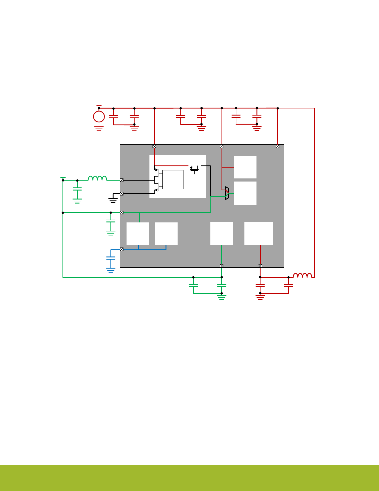
3.3 EFR32 Wireless Gecko Series 1 — DC-DC, 2.4 GHz, ≤ 13 dBm Example
Example Power Supply Configurations
EFM32
and EFR32 Wireless Gecko Series 1 applications should use the DC-DC converter to maximize power savings. The DC-DC
converter requires an external inductor and capacitor, in addition to the standard decoupling capacitors on each power net. For detailed
information on DC-DC converter operation, emlib programming, recommended DC-DC components, and supported power configurations, see application note AN0948: EFM32 and EFR32 Series 1 Power Configurations and DC-DC.
For the lowest power radio applications, the DC-DC converter can be used to supply DVDD, as well as RFVDD and PAVDD. In this
configuration:
• The DC-DC output (V
) is connected to DVDD, which powers the internal digital LDO (REGPWRSEL = 1 on
DCDC
EFR32xG12/13/14), and, therefore, the digital circuits.
• Both radio power supplies (RFVDD and PAVDD) are also powered from the DC-DC output.
• AVDD is connected to the main supply. Internal analog blocks may be powered from AVDD or DVDD, depending on the state of the
EMU_PWRCTRL_ANASW bit. Flash is always powered from the AVDD.
• IOVDD is connected to the main supply, although this is not required so long as VREGVDD ≥ IOVDD as discussed in 2.3 Power
Supply Requirements.
V
DD
C
IO
VDD
1 µF
Blocks
C
IO
0.1 µF
IOVDD
RF
Power
Amplifier
VDD1
V
DCDC
Main
Supply
4.7 µH
C
DCDC
4.7 µF
+
–
L
DCDC
C
DVDD
0.1 µF
C
VDD
10 µF
VREGVDD
VREGSW
VREGVSS
DVDD
C
VDD1
0.1 µF
Digital
LDO
DC-DC
Driver
Digital
Logic
C
A
VDD
10 µF
Bypass
Switch
OFF
DC-DC
C
AVDD1
10 nF
AVDD
FLASH
0
Analog
1
ANASW
RF
Analog
C
DEC
1 µF
DECOUPLE
RFVDD
C
RFVDD
220 nF
L
AVDD
P
22 nH
C
RFVDD
10 pF
C
PAVDD
1
PAVDD
220 nF
C
AVDD1
P
10 pF
Figure 3.5. EFR32xG1 DC-DC, 2.4 GHz, ≤ 13 dBm Example
Note: C
DCDC
1.0 µF in some previous revisions of this application note. Although 1.0 µF may still be used, 4.7 µF is now recom-
was
mended for new designs due to its improved performance under dynamic load conditions and during mode changes. Silicon Labs
EFR32xG1 reference radio boards still use 1.0 µF; therefore, the EFR32xG1 software defaults to using 1.0 µF (use of emuDcdcLnCompCtrl_1u0F rather than emuDcdcLnCompCtrl_4u7F). Use of 4.7 µF on EFR32xG1 requires modification of the Low Noise Mode
Compensator Control emuDcdcLnCompCtrl value. For EFR32xG12 and later, both the radio reference board hardware and the software default to 4.7 µF.
silabs.com | Building a more connected world. Rev. 1.55 | 15
Page 16

Main
Supply
AN0002.1: EFM32 and EFR32 Wireless Gecko Series 1 Hardware Design Considerations
Example Power Supply Configurations
V
DD
C
C
VDD
+
–
10 µF
VDD1
0.1 µF
C
A
VDD
C
AVDD1
10 µF 10 nF
C
1 µF
C
VDD1
IO
IO
VDD
0.1 µF
V
DCDC
L
DCDC
4.7 µH
C
DCDC
4.7 µF
C
DVDD
0.1 µF
C
DE
1 µF
1
REGPWRSEL
220 nF
AVDD
AVDD
1
Analog
Blocks
0
RFVDD
C
RFVDD
L
AVDD
P
22 nH
0
ANASW
RF
Analog
C
10 pF
FLASH
RFVDD
C
VREGVDD
VREGVDD
Bypass
Switch
OFF
DC-DC
VREGSW
VREGSW
VREGVSS
VREGVSS
DVDD
DVDD
Digital
Logic
DECOUPLE
C
DECOUPLE
Driver
DC-DC
Digital
LDO
Amplifier
PAVDD
1
PAVDD
220 nF
IOVDD
IOVDD
RF
Power
C
PAVDD1
10 pF
Figure 3.6. EFR32xG12/13/14 DC-DC, 2.4 GHz, ≤ 13 dBm Example
silabs.com | Building a more connected world. Rev. 1.55 | 16
Page 17
AN0002.1: EFM32 and EFR32 Wireless Gecko Series 1 Hardware Design Considerations
3.4 EFR32 Wireless Gecko Series 1 — DC-DC, 2.4 GHz, > 13 dBm Example
Example Power Supply Configurations
EFM32
converter requires an external inductor and capacitor, in addition to the standard decoupling capacitors on each power net. For detailed
information on DC-DC converter operation, emlib programming, recommended DC-DC components, and supported power configurations, see application note AN0948: EFM32 and EFR32 Series 1 Power Configurations and DC-DC.
When high radio output power (>13 dBm) is required, PAVDD must be connected to the main supply. DVDD and RFVDD can still be
supplied from the output of the DC-DC converter. This configuration is illustrated below.
and EFR32 Wireless Gecko Series 1 applications should use the DC-DC converter to maximize power savings. The DC-DC
V
DD
IO
VDD
C
IO
0.1 µF
IOVDD
RF
Power
Amplifier
VDD1
V
DCDC
Main
Supply
4.7 µH
C
DCDC
4.7 µF
+
–
L
DCDC
C
DVDD
0.1 µF
C
VDD
10 µF
VREGVDD
VREGSW
VREGVSS
DVDD
C
VDD1
0.1 µF
Digital
LDO
DC-DC
Driver
Digital
Logic
C
VDD
A
10 µF
Bypass
Switch
OFF
DC-DC
C
AVDD1
10 nF
AVDD
Analog
C
1 µF
FLASH
0
Analog
Blocks
1
ANASW
RF
C
DEC
1 µF
DECOUPLE
RFVDD
PAVDD
L
AVDD
P
22 nH
C
P
C
RFVDD
220 nF
Figure 3.7. EFR32xG1 DC-DC, 2.4 GHz, > 13 dBm Example
Note: C
mended for new designs due to its improved performance under dynamic load conditions and during mode changes. Silicon Labs
EFR32xG1 reference radio boards still use 1.0 µF; therefore, the EFR32xG1 software defaults to using 1.0 µF (use of emuDcdcLnCompCtrl_1u0F rather than emuDcdcLnCompCtrl_4u7F). Use of 4.7 µF on EFR32xG1 requires modification of the Low Noise Mode
Compensator Control emuDcdcLnCompCtrl value. For EFR32xG12 and later, both the radio reference board hardware and the software default to 4.7 µF.
DCDC
was
1.0 µF in some previous revisions of this application note. Although 1.0 µF may still be used, 4.7 µF is now recom-
C
RFVDD
10 pF
1
C
AVDD1
P
AVDD
220 nF10 pF
silabs.com | Building a more connected world. Rev. 1.55 | 17
Page 18

AN0002.1: EFM32 and EFR32 Wireless Gecko Series 1 Hardware Design Considerations
Example Power Supply Configurations
V
DD
Main
Supply
V
DCDC
+
–
L
DCDC
4.7 µH
C
DCDC
4.7 µF
C
DVDD
0.1 µF
C
DE
1 µF
IO
VDD
PAVDD
1
C
VDD1
IO
0.1 µF
IOVDD
IOVDD
RF
Power
Amplifier
C
PAVDD1
L
PAVDD
22 nH
C
P
AVDD
220 nF10 pF
0
RF
C
10 pF
C
1 µF
FLASH
RFVDD
C
10 µF
C
C
VDD
VDD1
0.1 µF
VREGVDD
VREGVDD
VREGSW
VREGSW
VREGVSS
VREGVSS
DVDD
DVDD
Digital
Logic
DECOUPLE
DECOUPLE
OFF
DC-DC
Driver
DC-DC
Digital
LDO
C
VDD
A
10 µF 10 nF
Bypass
Switch
1
C
AVDD1
AVDD
AVDD
1
ANASW
Analog
Blocks
0
REGPWRSEL
Analog
RFVDD
C
RFVDD
220 nF
Figure 3.8. EFR32xG12/13/14 DC-DC, 2.4 GHz, > 13 dBm Example
silabs.com | Building a more connected world. Rev. 1.55 | 18
Page 19

3.5 EFM32 Series 1 — DC-DC Example
AN0002.1: EFM32 and EFR32 Wireless Gecko Series 1 Hardware Design Considerations
Example Power Supply Configurations
The diagrams below illustrate a typical configuration for
EFM32 Series 1 devices using the DC-DC converter.
In this configuration:
• The DC-DC output (V
) is connected to DVDD, which powers the internal digital LDO (REGPWRSEL = 1 on EFM32xG11/12),
DCDC
and, therefore, the digital circuits.
• AVDD is connected to the main supply. The internal analog blocks may be powered from AVDD or DVDD, depending on the state of
the EMU_PWRCTRL_ANASW bit. Flash is always powered from the AVDD pin.
• IOVDD is connected to the main supply, although this is not required so long as VREGVDD ≥ IOVDD as discussed in 2.3 Power
Supply Requirements.
V
DD
C
IO
IO
VDD
VDD1
0.1 µF
IOVDD
AVDD_1
C
VDD2
A
10 nF
V
DCDC
Main
Supply
4.7 µH
C
DCDC
4.7 µF
+
–
L
DCDC
C
VDD
D
0.1 µF
C
VDD
10 µF
VREGSW
VREGVSS
DVDD
C
VDD1
0.1 µF
VREGVDD
Digital
LDO
DC-DC
Driver
Digital
Logic
C
A
VDD
10 µF
Bypass
Switch
OFF
DC-DC
C
AVDD1
10 nF
AVDD_0
C
1 µF
FLASH
0
Analog
Blocks
1
ANASW
C
DEC
DECOUPLE
1 µF
Figure 3.9. EFM32xG1 DC-DC Example
Note: C
DCDC
mended for new designs due to its improved performance under dynamic load conditions and during mode changes. The Silicon Labs
EFM32PG1 Starter Kit board still uses 1.0 µF; therefore, EFM32xG1 software defaults to using 1.0 µF (use of emuDcdcLnCompCtrl_1u0F rather than emuDcdcLnCompCtrl_4u7F). Use of 4.7 µF on EFM32xG1 requires modification of the Low Noise Mode
Compensator Control emuDcdcLnCompCtrl value. For all subsequent EFM32 devices, both the Starter Kit hardware and corresponding
software default to 4.7 µF.
1.0 µF in some previous revisions of this application note. Although 1.0 µF may still be used, 4.7 µF is now recom-
was
silabs.com | Building a more connected world. Rev. 1.55 | 19
Page 20

AN0002.1: EFM32 and EFR32 Wireless Gecko Series 1 Hardware Design Considerations
Example Power Supply Configurations
V
DD
Main
Supply
V
DCDC
+
–
L
DCDC
4.7 µH
C
DCDC
4.7 µF
C
DVDD
0.1 µF
C
DE
1 µF
C
10 µF
C
C
VDD
VDD1
0.1 µF
VREGVDD
VREGVDD
VREGSW
VREGSW
VREGVSS
VREGVSS
DVDD
DVDD
Digital
Logic
DECOUPLE
DECOUPLE
OFF
DC-DC
Driver
DC-DC
Digital
LDO
C
A
VDD
10 µF 10 nF
Bypass
Switch
1
C
AVDD1
AVDD
AVDD
1
ANASW
Analog
Blocks
0
REGPWRSEL
C
1 µF
FLASH
0
C
VDD1
IO
VDD
IO
0.1 µF
IOVDD
IOVDD
Figure 3.10. EFM32xG11/12 DC-DC Example
silabs.com | Building a more connected world. Rev. 1.55 | 20
Page 21

AN0002.1: EFM32 and EFR32 Wireless Gecko Series 1 Hardware Design Considerations
Debug Interface and External Reset Pin
4. Debug Interface and External Reset Pin
4.1 Serial Wire Debug
The Serial Wire Debug (SWD) interface is supported by all EFM32 and EFR32 Wireless Gecko Series 1 devices and consists of the
SWCLK (clock input) and SWDIO (data in/out) lines, in addition to the optional SWO (serial wire output). The SWO line is used for
instrumentation trace and program counter sampling, and is not needed for flash programming and normal debugging. However, it can
be valuable in advanced debugging scenarios, and designers are strongly encouraged to include this along with the other SWD signals.
Connections to the standard ARM 20-pin debug header are shown in the following figure. Pins that are not connected to the microcontroller, power supply, or ground should be left unconnected.
VMCU
VDD
RESETn
Gecko Device
PF1
PF0
PF2
VSS
SWDIO
SWCLK
SWO
Reset
VMCU
Vtarget
1 2
3 4
5 6
7 8
9 10
11 12
13 14
15 16
17 18
19 20
ARM 20 Pin Header
Figure 4.1. EFM32 and EFR32 Wireless Gecko Series 1 SWD Connection to the ARM 20-pin Debug Header
Note:
The V
1.
2. PF2 is the default location for the SWO signal and is adjacent or in close proximity to PF0 (SWCLK) and PF1 (SWDIO) on any
given package. SWO can be mapped to certain other pins. Refer to the datasheet for the device in question.
connection does not supply power. The debugger uses V
target
as a reference voltage for its level translators.
target
For additional debug and programming interfaces, see Application Note AN958: Debugging and Programming Interfaces for Custom
Designs.
silabs.com | Building a more connected world. Rev. 1.55 | 21
Page 22

4.2 JTAG Debug
AN0002.1: EFM32 and EFR32 Wireless Gecko Series 1 Hardware Design Considerations
Debug Interface and External Reset Pin
EFM32
and EFR32 Wireless Gecko Series 1 devices optionally support JTAG debug using the TCK (clock), TDI (data input), TDO (data output), and TMS (input mode select) lines. TCK is the JTAG interface clock. TDI carries input data and is sampled on the rising
edge of TCK. TDO carries output data and is shifted out on the falling edge of TCK. Finally, TMS is the input mode select signal, and is
used to navigate through the Test Access Port (TAP) state machine.
Note: The JTAG implementation on EFM32 and EFR32 Wireless Gecko Series 1 devices does not support boundary scan testing. It
can operate in pass-through mode and participate in a chain with other devices that do implement JTAG for firmware programming or
boundary scan purposes.
The connection to an ARM 20-pin debug connector is shown in the following figure. Pins with no connection should be left unconnected.
VMCU
IOVDD
RESETn
Gecko Device
PF3
PF1
PF0
PF2
VSS
TDI
TMS
TCK
TDO
Reset
VMCU
Vtarget
1 2
3 4
5 6
7 8
9 10
11 12
13 14
15 16
17 18
19 20
ARM 20 Pin Header
Figure 4.2. EFM32 and EFR32 Wireless Gecko Series 1 JTAG Connection to the ARM 20-pin Debug Header
Note: The V
additional debug and programming interfaces, see Application Note AN958: Debugging and Programming Interfaces for Custom
For
Designs.
4.3 External Reset Pin (RESETn)
EFM32 and EFR32 Wireless Gecko Series 1 processors are reset by driving the RESETn pin low. A weak internal pull-up device holds
the RESETn pin high, allowing it to be left unconnected if no external reset source is required. Also connected to RESETn is a low-pass
filter to prevents noise glitches from causing unintended resets. The characteristics of the pull-up device and input filter are identical to
those present on any GPIO pin and are specified in the device data sheet.
Note: The internal pull-up ensures that the reset is released. When the device is not powered, RESETn must not be connected through
an external pull-up to an active supply or otherwise driven high as this could damage the device. This is especially critical when using
back-up power mode. Because the internal pull-up device is automatically switched to the back-up power rail, it can back-power other
devices in the system through an external pull-up connected to RESETn.
connection does not supply power. The debugger uses V
target
as a reference voltage for its level translators.
target
silabs.com | Building a more connected world. Rev. 1.55 | 22
Page 23

AN0002.1: EFM32 and EFR32 Wireless Gecko Series 1 Hardware Design Considerations
External Clock Sources
5. External Clock Sources
5.1 Introduction
EFM32 and EFR32 Wireless Gecko Series 1 devices support different external clock sources to provide the high- and low-frequency
clocks in addition to the internal LF and HF RC oscillators. Possible external clock sources for both the LF and HF domains are crystals,
ceramic resonators, and external oscillators (square or sine wave). This section describes how external clock sources are connected.
For additional information on the external oscillators, refer to the application note, AN0016.1: Oscillator DesignConsiderations. Application notes can be found on the Silicon Labs website (www.silabs.com/32bit-appnotes) or in Simplicity Studio.
5.2 Low-Frequency Clock Sources
An external low-frequency clock can be supplied from a crystal or ceramic resonator or from an external clock source.
5.2.1 Low-Frequency Crystals
A crystal is connected as shown in the figure below across the LFXTAL_N and LFXTAL_P pins on EFM32 and EFR32 Wireless Gecko
Series 1 devices.
LFXTAL_N
C
C
TUNING
TUNING
32.768 kHz
LFXTAL_P
Gecko Device
Figure 5.1. Low-Frequency Crystal Oscillator
Low frequency crystals connected to EFM32 and EFR32 Wireless Gecko Series 1 devices do not require external load capacitors, as
load capacitors are included on-chip and can be tuned by register bit fields under software control, thus reducing BOM cost and
these
saving space in the PCB footprint. The EFM32 and EFR32 Wireless Gecko Series 1 LFXO supports 32.768 kHz crystals. Check device-specific data sheets for supported crystal load capacitance and ESR values and refer to device-specific reference manuals for onchip load capacitor tuning instructions.
silabs.com | Building a more connected world. Rev. 1.55 | 23
Page 24

5.2.2 Low-Frequency External Clocks
AN0002.1: EFM32 and EFR32 Wireless Gecko Series 1 Hardware Design Considerations
External Clock Sources
EFM32
and EFR32 Wireless Gecko Series 1 devices can source a low-frequency clock from an external source such as a TCXO or
VCXO. To select a proper external oscillator, consider specifications such as frequency, aging, stability, voltage sensitivity, rise and fall
time, duty cycle, and signal levels. The external clock signal can be either a square wave or a sine wave with a frequency of 32.768
kHz. The external clock source must be connected as shown in Figure 5.2 Low-Frequency External Clock on page 24.
Bypass and buffered input modes are supported for external clock sources. A CMOS square wave that toggles between 0 and V
IOVDD
volts with a duty cycle of 50% can be used when CMU_LFXOCTRL_MODE = DIGEXTCLK, which bypasses the LFXO. An external
sine wave source (CMU_LFXOCTRL_MODE = BUFEXTCLK) having minimum and maximum amplitudes of 800 mV and 1.2 volts, respectively, can be connected in series with the LFXTAL_N pin and is AC-coupled internally. The sine wave minimum voltage must be
higher than ground and the maximum voltage less than 1.4 volts.
External
32.768 kHz
Clock Source
LFXTAL_N
LFXTAL_P
(High-Z)
Gecko Device
Figure 5.2. Low-Frequency External Clock
5.3 High Frequency Clock Sources
An external high-frequency clock can be supplied from a
crystal or ceramic resonator or from an external clock source.
5.3.1 High-Frequency Crystals and Ceramic Resonators
A crystal or ceramic resonator is connected as shown in Figure 5.3 High-Frequency Crystal Oscillator on page 24 across the
HFXTAL_N and HFXTAL_P pins on EFM32 and EFR32 Wireless Gecko Series 1 devices.
External load capacitors are not required on EFM32 and EFR32 Wireless Gecko Series 1 devices. These have been moved on-chip
and can be tuned by register bit fields under software control, thus reducing BOM cost and saving space in the PCB footprint. Check
device-specific data sheets for the supported range of crystal frequencies, load capacitance tuning, and ESR values. In particular, specific crystal frequencies are mandatory when using on-chip radios and their associated protocol stacks; use of other values is expressly
not supported.
HFXTAL_N
C
TUNING
HFXTAL_P
C
TUNING
Gecko Device
Figure 5.3. High-Frequency Crystal Oscillator
silabs.com | Building a more connected world. Rev. 1.55 | 24
Page 25

5.3.2 High Frequency External Clocks
AN0002.1: EFM32 and EFR32 Wireless Gecko Series 1 Hardware Design Considerations
External Clock Sources
EFM32
VCXO. To select a proper external oscillator, consider specifications such as frequency, aging, stability, voltage sensitivity, rise and fall
time, duty cycle, and signal levels. The external clock signal can be either a square wave or a sine wave with a frequency in accordance with the device data sheet. The external clock source must be connected as shown in Figure 5.4 External High-Frequency Clock
on page 25.
Unlike the LFXO, which has specific modes for a buffered or digital external clock, some EFM32 and EFR32 Wireless Gecko Series 1
devices have more limited high-frequency clock input options. On all such devices, an externally-buffered sine wave having minimum
and maximum amplitudes of 800 mV and 1.2 V, respectively, can be connected in series with the HFXTAL_N pin. The sine wave minimum voltage must be higher than ground and the maximum voltage less than 1.4 V. Refer to the device-specific datasheet and reference manual for the options and limitations that apply when sourcing a high-frequency clock.
and EFR32 Wireless Gecko Series 1 devices can source a low-frequency clock from an external source such as a TCXO or
External
Clock Source
HFXTAL_N
HFXTAL_P
(High-Z)
Gecko Device
Figure 5.4. External High-Frequency Clock
silabs.com | Building a more connected world. Rev. 1.55 | 25
Page 26

AN0002.1: EFM32 and EFR32 Wireless Gecko Series 1 Hardware Design Considerations
USB
6. USB
Some EFM32 Series 1 devices integrate a USB controller and a 3.3V LDO. The following sections illustrate several different configurations for decoupling the USB power and connecting the bus and control signals.
To avoid violating the USB specification, the total capacitance on V
must not exceed 10 µF. Consult AN0046: USB Hardware De-
USB
sign Guide for detailed hardware guidance for USB applications.
6.1 USB Self-Powered
In a typical EFM32 Series 1 self-powered USB device application, the internal 3.3 V LDO powers the PHY only (although it may also be
used to power other external components), and the rest of the system is powered from an external 1.8 V to 3.8 V supply. Note that per
USB compliance specifications, the supply to the USB PHY must meet be between 3.0 V and 3.6 V.
If unused, the VREGI input may be left floating; a weak internal pull-down ensures that this pin remains at ground.
Bypass capacitors unrelated to USB are not shown below.
USB
Jack
VREGI
= 5V
V
USB
ESD
Protection
VBUS
USB 5V
Sense
USB_DP
USB_DM
1
3.3V
LDO
AVDD/
VREGVDD/
DVDD
IOVDD
2
Bypass
Switch
VREGO
USB Core &
PHY
/
V
VREGO
External Supply
(1.8V – 3.8V)
= 3.3V
Note: EFM32GG11 devices prior to Rev B require zero series resistance on USB_DP and USB_DM.
Figure 6.1. Self-Powered USB Application
silabs.com | Building a more connected world. Rev. 1.55 | 26
Page 27

AN0002.1: EFM32 and EFR32 Wireless Gecko Series 1 Hardware Design Considerations
USB
6.2 USB Bus-Powered
typical EFM32 Series 1 USB bus-powered device configuration is shown in Figure 6.2 Bus-Powered USB Application on page 27.
A
In this configuration, the internal 3.3 V LDO is connected to the USB 5 V supply and powers both the USB PHY and the EFM32 Series
1 at 3.3 V. The voltage regulator output (VREGO) may also be used to power other components in the system. Note that per USB
compliance specifications, the supply to the USB PHY must meet be between 3.0 V and 3.6 V.
If unused, the VREGI input may be left floating; a weak internal pull-down ensures that this pin remains at ground.
Bypass capacitors unrelated to USB are not shown below.
USB
Jack
VREGI
= 5V
V
USB
ESD
Protection
VBUS
USB 5V
Sense
USB_DP
USB_DM
1
3.3V
LDO
AVDD/
VREGVDD/
DVDD/
IOVDD
2
Bypass
Switch
VREGO
USB Core &
PHY
V
VREGO
= 3.3V
Note: EFM32GG11 devices prior to Rev B require zero series resistance on USB_DP and USB_DM.
Figure 6.2. Bus-Powered USB Application
silabs.com | Building a more connected world. Rev. 1.55 | 27
Page 28

AN0002.1: EFM32 and EFR32 Wireless Gecko Series 1 Hardware Design Considerations
USB
6.3 USB Dual-Powered
dual-powered USB configuration is shown in Figure 6.3 Dual-Powered USB Application on page 28. This configuration is useful for
A
extending the life of battery-powered devices, as it allows a battery- or externally-powered device to switch its power supply to the USB
5 V supply when connected to a USB host. An internal switch permits the 3.3 V LDO input to be seamlessly switched between a battery
(or other external supply) on the VREGI pin and the USB 5 V supply on the VBUS pin.
Typically, firmware would configure the 3.3 V LDO to be powered from the higher of the two supply inputs (VREGI or VBUS). When
unused, or unconnected, the VREGI and VBUS inputs are pulled to ground through a weak internal pull-downs.
Bypass capacitors unrelated to USB are not shown below.
External Supply
(3.6V – 5.0V)
VREGI
= 5V
V
USB
VBUS
1
AVDD/
VREGVDD/
DVDD/
IOVDD
2
3.3V
LDO
Bypass
Switch
VREGO
USB Core &
PHY
V
VREGO
= 3.3V
USB
Jack
USB 5V
Sense
ESD
Protection
USB_DP
USB_DM
Note: EFM32GG11 devices prior to Rev B require zero series resistance on USB_DP and USB_DM.
Figure 6.3. Dual-Powered USB Application
6.4 USB Host
typical EFM32 Series 1 host configuration using an external 5 V step-up regulator is shown in Figure 6.4 Host USB Application on
A
page 28. In this configuration, the internal 3.3 V LDO is unused, and the VREGO pin is driven directly from an external 3.0 V to 3.6 V
source. The VREGI input is left floating; a weak internal pull-down ensures this pin remains at ground. The VBUS input is still used to
detect the 5 V supply.
In host mode, the minimum USB 5 V decoupling capacitance is 120 µF. Bypass capacitors unrelated to USB are not shown below.
V
USB
Jack
USB
= 5V
Protection
5V Step-Up
C
VBUSHOST
120 µF
ESD
15 Ω
15 Ω
OVERCURRENT
Regulator
EN
VINVOUT
VREGI
VBUS
1
USB 5V
Sense
USB_DP
USB_DM
USB_ID
USB_VBUSEN
GPIO
3.3V
LDO
AVDD/
VREGVDD/
DVDD/
IOVDD
2
Bypass
Switch
VREGO
USB Core &
PHY
External Supply
(3.0V – 3.6V)
Note: EFM32GG11 devices prior to Rev B require zero series resistance on USB_DP and USB_DM.
Figure 6.4. Host USB Application
silabs.com | Building a more connected world. Rev. 1.55 | 28
Page 29

AN0002.1: EFM32 and EFR32 Wireless Gecko Series 1 Hardware Design Considerations
Backup Power Domain
7. Backup Power Domain
7.1 Overview
EFM32 Series 1 Giant Gecko and Tiny Gecko devices can be partly powered by a backup battery. These devices have a dedicated
power domain for the RTCC and its 128 bytes of retention registers along with the CRYOTIMER that can be retained in the event main
power is lost. When this happens, the system enters a low energy mode, equivalent to EM4 Hibernate, and automatically switches over
to the backup power supply.
Note: The power supply relationship requirements given in 2.3 Power Supply Requirements must always be adhered to. This means
that even when the main supply (VREGVDD/AVDD) falls, these relationships must stay valid, e.g. AVDD ≥ IOVDD in all scenarios.
7.2 Connections
The backup power domain interface consists of three pins. BU_VIN is connected directly to the backup power supply and is the only
one required for operation. BU_VOUT can power external devices from the backup supply, while BU_STAT is simply driven to BU_VIN
when backup mode is active and to ground otherwise.
EFM32
EMU_BUCTRL_EN
VMON AVDD fall trigger
EMU_BUCTRL_STATEN
BU_STAT
Main
power
supply
AVDD
+
-
EMU_BUCTRL_BUACTPWRCON /
EMU_BUCTRL_BUINACTPWRCON
VMON AVDD
Main power
Main domain
EMU_BUCTRL_PWRRES
Backup regulator
Backup domain
RTCC
128 byte
retention
CRYOTIMER
Backup power
STRONG
MEDIUM
WEAK
EMU_BUCTRL_VOUTRES
VMON BUVDD
BU_VIN
BU_VOUT
+
-
Backup
power
supply
Figure 7.1. Backup Power Domain
Note: All
three pins are shared with GPIO and peripheral functionality and each must be configured as follows for proper backup do-
main operation:
• Disabled via its mode register (GPIO_Px_MODEL/GPIO_Px_MODEH)
• Output set to 0 in GPIO_Px_DOUT (if set, the pin is pulled up, even when disabled)
• Locked by setting its respective bit in GPIO_Px_PINLOCKN
silabs.com | Building a more connected world. Rev. 1.55 | 29
Page 30

AN0002.1: EFM32 and EFR32 Wireless Gecko Series 1 Hardware Design Considerations
Backup Power Domain
Allowable sources for the backup supply input include batteries and supercapacitors with output voltages in the same range as that
permitted
also be connected to the BU_VOUT pin and powered by the backup power supply along with the on-chip backup domain when main
power fails.
Note: When using this feature, it is imperative that such circuits are not connected to or are otherwise electrically isolated from the rest
of the system. Failure to observe this requirement will result in some level of back-powering and rapid depletion of the backup supply.
for the device. Charging of the backup power source via the main power supply is possible. Low current external circuitry can
silabs.com | Building a more connected world. Rev. 1.55 | 30
Page 31

AN0002.1: EFM32 and EFR32 Wireless Gecko Series 1 Hardware Design Considerations
Revision History
8. Revision History
Revision 1.55
January 2021
•
Updated application note references.
Revision 1.54
June 2020
• Added EFM32GG12.
• Corrected required amplitude of a sine wave oscillator input in 5.2.2 Low-Frequency External Clocks and 5.3.2 High Frequency Ex-
ternal Clocks.
Revision 1.53
December 2019
• Added reference to AN958 in 4.1 Serial Wire Debug and 4.2 JTAG Debug.
• Corrected minor typos throughout the document.
Revision 1.52
August 2018
• Updated series resistance on USB_DP and USB_DM to 33 ohms, except in the case of EFM32GG11 rev A/X (which requires zero
ohms).
Revision 1.51
May 2018
• Clarified that the PAVDD pin is only the supply input for the 2.4 GHz power amplifier (for sub-GHz, the power amplifier is powered
externally).
Revision 1.50
January 2018
• Removed EFM32JG13 and EFM32PG13 part compatibility.
• The note regarding decoupling capacitors in has been reworded to reflect what the EFM32PG1 Starter Kit uses versus the Starter
Kits for subsequent EFM32 Series 1 devices.
Revision 1.49
September 2017
• Added references to EFR32xG14.
• Added references to EFM32TG11.
• Added backup domain section.
• Section High Frequency External Clocks rewritten to reflect differences between EFM32xG1 and EFR32xG1 and later Series 1 family members.
Revision 1.48
June 2017
• Added reference to EFM32GG11.
• Added VBUS to Power Supply Pin Overview.
• Renamed USB_VREGO and USB_VREGI to VREGO and VREGI.
• Added Section USB.
silabs.com | Building a more connected world. Rev. 1.55 | 31
Page 32

AN0002.1: EFM32 and EFR32 Wireless Gecko Series 1 Hardware Design Considerations
Revision History
Revision 1.47
January 2017
Split application note into multiple application notes, based on family.
•
• Updated content for EFM32xG11/12 and EFR32xG12/13/14 devices.
• Changed default DCDC output capacitor from 1.0 uF to 4.7 uF.
• Added note advising the system designer to check the capacitance vs temperature characteristics for regulator and dc-dc output
capacitors.
silabs.com | Building a more connected world. Rev. 1.55 | 32
Page 33

Simplicity Studio
One-click access to MCU and wireless
tools, documentation, software, source
code libraries & more. Available for
Windows, Mac and Linux!
IoT Portfolio
www.silabs.com/IoT
Disclaimer
Silicon Labs intends to provide customers with the latest, accurate, and in-depth documentation of all peripherals and modules available for system and software implementers using or
intending to use the Silicon Labs products. Characterization data, available modules and peripherals, memory sizes and memory addresses refer to each specific device, and “Typical”
parameters provided can and do vary in different applications. Application examples described herein are for illustrative purposes only. Silicon Labs reserves the right to make changes
without further notice to the product information, specifications, and descriptions herein, and does not give warranties as to the accuracy or completeness of the included information.
Without prior notification, Silicon Labs may update product firmware during the manufacturing process for security or reliability reasons. Such changes will not alter the specifications or
the performance of the product. Silicon Labs shall have no liability for the consequences of use of the information supplied in this document. This document does not imply or expressly
grant any license to design or fabricate any integrated circuits. The products are not designed or authorized to be used within any FDA Class III devices, applications for which FDA
premarket approval is required, or Life Support Systems without the specific written consent of Silicon Labs. A “Life Support System” is any product or system intended to support or
sustain life and/or health, which, if it fails, can be reasonably expected to result in significant personal injury or death. Silicon Labs products are not designed or authorized for military
applications. Silicon Labs products shall under no circumstances be used in weapons of mass destruction including (but not limited to) nuclear, biological or chemical weapons, or
missiles capable of delivering such weapons. Silicon Labs disclaims all express and implied warranties and shall not be responsible or liable for any injuries or damages related to use of
a Silicon Labs product in such unauthorized applications.
Trademark Information
Silicon Laboratories Inc.®, Silicon Laboratories®, Silicon Labs®, SiLabs® and the Silicon Labs logo®, Bluegiga®, Bluegiga Logo®, ClockBuilder®, CMEMS®, DSPLL®, EFM®,
EFM32®, EFR, Ember®, Energy Micro, Energy Micro logo and combinations thereof, “the world’s most energy friendly microcontrollers”, Ember®, EZLink®, EZRadio®, EZRadioPRO®,
Gecko®, Gecko OS, Gecko OS Studio, ISOmodem®, Precision32®, ProSLIC®, Simplicity Studio®, SiPHY®, Telegesis, the Telegesis Logo®, USBXpress®, Zentri, the Zentri logo and
Zentri DMS, Z-Wave®, and others are trademarks or registered trademarks of Silicon Labs. ARM, CORTEX, Cortex-M3 and THUMB are trademarks or registered trademarks of ARM
Holdings. Keil is a registered trademark of ARM Limited. Wi-Fi is a registered trademark of the Wi-Fi Alliance. All other products or brand names mentioned herein are trademarks of
their respective holders.
Silicon Laboratories Inc.
400 West Cesar Chavez
Austin, TX 78701
USA
http: //www.silabs.com
SW/HW
w.silabs.com/simplicity
ww
Quality
w.silabs.com/quality
ww
Support & Community
www.silabs.com/community
 Loading...