


WT41u
DATA SHEET
Friday, 03 February 2017
Version 1.0

VERSION HISTORY
Version Comment
0.8 First version
0.8.1 Table reformatting, value updates etc
0.8.2 Replaced “Bluecore4” with “chipset”, added ordering codes
0.8.3 Rest of table reformatting, added antenna & connector dimension drawings
0.8.4 Added current consumption, RF characteristics
0.8.5 Added certification texts
0.8.6 Added current consumption results, edit TX power variation over VDD range.
0.8.7 Slight edits to specifications
0.8.8 OPN descriptions updated
1.0 Full production
Silicon Labs

TABLE OF CONTENTS
1 Ordering Information......................................................................................................................................6
2 Pinout and Terminal Description ...................................................................................................................7
3 Electrical Characteristics ............................................................................................................................ 11
3.1 Absolute Maximum Ratings ................................................................................................................ 11
3.2 Recommended Operating Conditions ................................................................................................. 11
3.3 Input / Output Terminal Characteristics .............................................................................................. 12
3.3.1 Input/Output Terminal Characteristics (Digital) ............................................................................ 12
3.3.2 Input/Output Terminal Characteristics (USB) .............................................................................. 13
3.4 PIO Current Sink and Source Capability ............................................................................................. 13
3.5 Transmitter Performance For BDR ..................................................................................................... 14
3.6 Receiver Performance ........................................................................................................................ 15
3.7 Current Consumption .......................................................................................................................... 15
4 Physical Dimensions .................................................................................................................................. 16
5 Soldering Recommendations ..................................................................................................................... 19
6 Layout Guidelines ....................................................................................................................................... 20
7 UART Interface ........................................................................................................................................... 21
7.1 UART Bypass ...................................................................................................................................... 23
7.2 UART Configuration While Reset is Active ......................................................................................... 23
7.3 UART Bypass Mode ............................................................................................................................ 23
8 USB Interface ............................................................................................................................................. 24
8.1 USB Data Connections ....................................................................................................................... 24
8.2 USB Pull-Up resistor ........................................................................................................................... 24
8.3 USB Power Supply .............................................................................................................................. 24
8.4 Self-Powered Mode ............................................................................................................................. 24
8.5 Bus-Powered Mode ............................................................................................................................. 25
8.6 USB Suspend Current ......................................................................................................................... 26
8.7 USB Detach and Wake-Up Signaling.................................................................................................. 26
8.8 USB Driver .......................................................................................................................................... 27
8.9 USB v2.0 Compliance and Compatibility ............................................................................................ 27
9 Serial Peripheral Interface (SPI) ................................................................................................................. 28
10 PCM Codec Interface ............................................................................................................................. 29
10.1 PCM Interface Master/Slave ........................................................................................................ 29
10.2 Long Frame Sync ......................................................................................................................... 30
10.3 Short Frame Sync ........................................................................................................................ 30
10.4 Multi-slot Operation ...................................................................................................................... 31
10.5 GCI Interface ................................................................................................................................ 31
10.6 Slots and Sample Formats ........................................................................................................... 32
Silicon Labs

10.7
Additional Features ...................................................................................................................... 33
10.8 PCM_CLK and PCM_SYNC Generation ..................................................................................... 33
10.9 PCM Configuration ....................................................................................................................... 34
11 I/O Parallel Ports ..................................................................................................................................... 37
11.1 PIO Defaults ................................................................................................................................. 37
12 Reset ....................................................................................................................................................... 38
12.1 Pin States on Reset ..................................................................................................................... 39
13 Certifications ........................................................................................................................................... 40
13.1 Bluetooth ...................................................................................................................................... 40
13.2 FCC .............................................................................................................................................. 40
13.3 ISEDC .......................................................................................................................................... 41
13.3.1 ISEDC (Français) ......................................................................................................................... 41
13.4 CE ................................................................................................................................................ 42
13.5 MIC Japan .................................................................................................................................... 43
13.6 Qualified Antenna Types for WT41u-E and WT41u-N ................................................................ 44
13.7 Moisture Sensitivity Level (MSL).................................................................................................. 44
Silicon Labs

WT41u Bluetooth® Module
DESCRIPTION
WT41u is a long range class 1, Bluetooth® 2.1 +
EDR module. WT41u is a highly integrated and
sophisticated Bluetooth® module, containing all the
necessary elements from Bluetooth® radio and a
fully implemented protocol stack. Therefore, WT41u
provides an ideal solution for developers who want
to integrate Bluetooth® wireless technology into
their design with limited knowledge of Bluetooth®
and RF technologies. WT41u is optimized for long
range applications is available with an integrated
chip antenna, an RF pin for a custom on-board
antenna or a U.FL connector for an external 2dBi
dipole antenna.
By default, WT41u module is equipped with
powerful and easy-to-use iWRAP firmware. iWRAP
enables users to access Bluetooth® functionality
with simple ASCII commands delivered to the
module over serial interface - it's just like a
Bluetooth® modem.
APPLICATIONS:
• Hand held terminals
• Industrial devices
• Point-of-Sale systems
• PCs
• Personal Digital Assistants (PDAs)
• Computer Accessories
• Access Points
• Automotive Diagnostics Units
FEATURES:
• Fully Qualified Bluetooth v2.1 + EDR end
product
• CE qualified
• Full modular certification for FCC and IC
• MIC Japan compatibility fully tested with ARIB
STD-T66
• TX power: 17 dBm
• RX sensitivity: -94 dBm
• Integrated chip antenna, RF pin or U.FL
antenna connector
• Class 1, range up to 650 meters with chip
antenna or up to 1km with an external dipole
• Industrial temperature range from -40
• RoHS Compliant
• USB interface (USB 2.0 compatible)
• UART with bypass mode
• 6 x GPIO
• 1 x 8-bit AIO
• Integrated iWRAP
o
C
+85
firmware
TM
Bluetooth stack or HCI
o
C to
Silicon Labs

1 Ordering Information
Firmware U.FL Connector Internal chip antenna
iWRAP 5.6 firmware WT41u-E-AI56 WT41u-A-AI56
iWRAP 5.5 firmware WT41u-E-AI55 WT41u-A-AI55
iWRAP 5.0.2 firmware WT41u-E-AI5 WT41u-A-AI5
HCI firmware, BT2.1 + EDR WT41u-E-HCI21 WT41u-A-HCI21
Table 1: Ordering information
Silicon Labs
Page 6 of 44
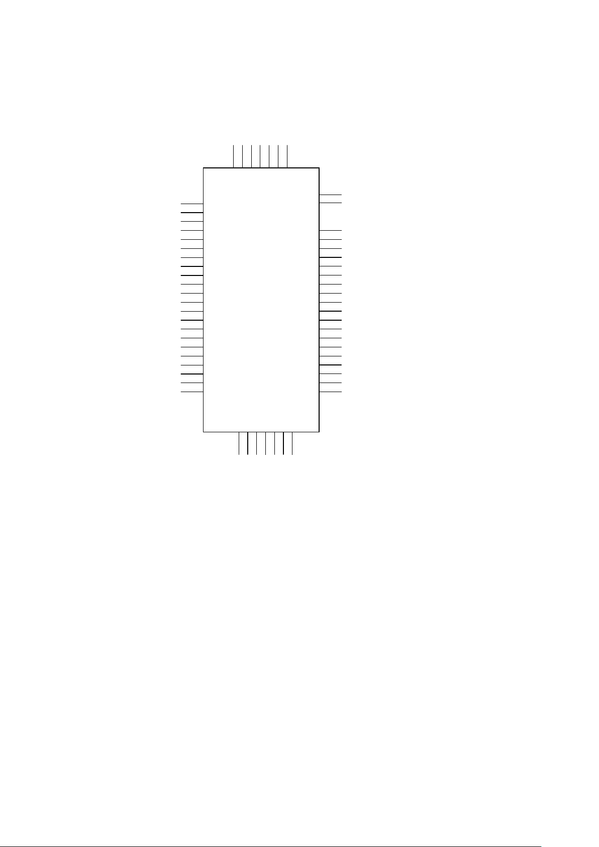
Pins 1 and 52 (GND)
are not connected
and have been
removed
2
3
4
5
6
7
8
9
10
11
12
13
14
15
16
17
18
19
20
21
22
23
24
25
262728
29
51
49
48
47
46
45
44
43
42
41
40
39
38
37
36
35
34
33
32
31
30
59
5857565554
53
GND
GND
GND
GND
GND
GND
GND
GND
GND
GND
GND
GND
GND
GND
GND
GND
RFGND
RF
GND
GND
GND
GND
GND
GND
VDD_PA
PIO2
PIO3
UART_RTS
UART_RX
GND
USB+
USBUART_CTS
PCM_IN
PCM_CLK
PCM_SYNC
GND
GND
GND
GND
GND
GND
PCM_OUT
PIO4
GND
VDD
RESET
PIO6
PIO7
GND
SPI_CSB
SPI_CLK
SPI_MISO
SPI_MOSI
PIO5
UART_TX
AIO
50
2 Pinout and Terminal Description
Figure 1: WT41u pin out
Silicon Labs
Page 7 of 44
Pad name Pad
Pad type Description
number
NC 1, 52 Not connected Pins 1 and 52 are not present on the footprint
RESET 33 Digital input Active low reset with weak internal pull-up. Ke ep
low for >5ms to reset module
GND 2-10, 16, 23,
24, 26-28,
30, 31, 36,
Ground Ground pads should all be connected to a ground
plane with minimum trace length, especially on the
antenna end of the module
44-49, 53-
59
RF 51 Not connected No internal connection
RFGND 50 Ground Connect to ground plane
VDD_PA 11 Supply voltage Supply voltage for the RF power amplifier and low
noise amplifier
VDD 32 Supply voltage Supply voltage for the Bluetooth chipset
Table 2: Supply and RF Terminal Descriptions
PIO signal Pad number Description
PIO[2] 12 Bi-directional digital in/out with programmable strength and pull-up/pull-
down
PIO[3] 13 Bi-directional digital in/out with programmable strength and pull-up/pull-
down
PIO[4] 29 Bi-directional digital in/out with programmable strength and pull-up/pull-
down
PIO[5] 41 Bi-directional digital in/out with programmable strength and pull-up/pull-
down
PIO[6] 34 Bi-directional digital in/out with programmable strength and pull-up/pull-
down
PIO[7] 35 Bi-directional digital in/out with programmable strength and pull-up/pull-
down
AIO[1] 43 Bi-directional analog in/out
Table 3: GPIO Terminal Descriptions
Silicon Labs
Page 8 of 44
Output, weak internal
Output, weak internal
UART request to send,
UART data input, active
UART clear to send,
PCM signal Pad number Pad type Description
PCM_OUT 25 Output, weak internal pull-down Synchronous data output
PCM_IN 20 Input, weak internal pull-down Synchronous data input
PCM_SYNC 22 Bi-directional, weak internal pull-down Synchronous data sync
PCM_CLK 21 Bi-directional, weak internal pull-down Synchronous data clock
Table 4: PCM Terminal Descriptions
UART signal Pad number Pad type Description
UART_TX 42
pull-up
UART data output, active
high
UART_RTS# 14
pull-up
active low
UART_RX 15 Input, weak internal pull-
down
high
UART_CTS# 19 Input, weak internal pull-
down
active low
Table 5: UART Terminal Descriptions
USB signal Pad number Pad type Description
USB+ 17 Bidirectional USB data line with internal 1.5kohm pull-up
USB- 18 Bidirectional USB data line
Table 6: USB Terminal Descriptions
Silicon Labs
Page 9 of 44

SPI signal Pad
Pad type Description
number
SPI_MOSI 40 Input, weak internal pull-down SPI data input
SPI_CS# 37 Input, weak internal pull-up Chip select, active low
SPI_CLK 38 Input, weak internal pull-down SPI clock
SPI_MISO 39 Output, weak internal pull-down SPI data output
Table 7: Terminal Descriptions
Silicon Labs
Page 10 of 44
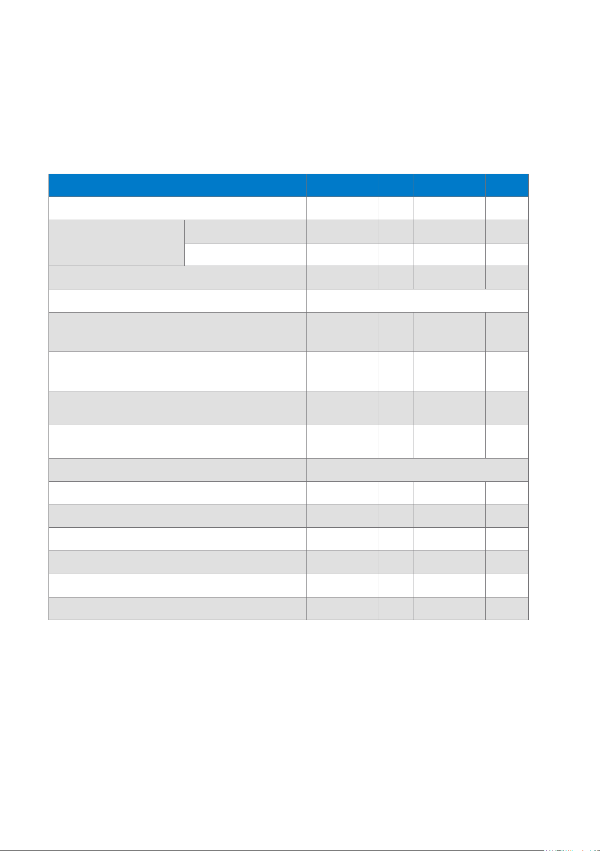
3 Electrical Characteristics
3.1 Absolute Maximum Ratings
Specification Min Max Unit
Storage temperature -40 85 °C
VDD_PA, VDD -0.4 3.7 V
Other terminal voltages VSS-0.4 VDD+0.4 V
Table 8: Absolute Maximum Ratings
3.2 Recommended Operating Conditions
Specification Min Max Unit
Operating temperature -40 85 °C
VDD_PA, VDD 3.0 3.6 V
Table 9: Recommended Operating Conditions
Silicon Labs
Page 11 of 44
3.3 Input / Output Terminal Characteristics
3.3.1 Input/Output Terminal Characteristics (Digital)
Digital Terminals Min Typ Max Unit
Input Voltage Levels
VIL input logic level low 2.7 V ≤ VDD ≤ 3.0 V -0.4 - 0.8 V
1.7 V ≤ VDD ≤ 1.9 V -0.4 - 0.4 V
VIH input logic level high 0.7 VDD - VDD + 0.4 V
Output Voltage Levels
VOL output logic level low
(IO = 4.0 mA) 2.7V ≤ VDD ≤ 3.0 V
VOL output logic level low
(IO = 4.0 mA) 1.7V ≤ VDD ≤ 1.9
VOL output logic level high
(IO = 4.0 mA) 2.7V ≤ VDD ≤ 3.0
VOL output logic level high
(IO = 4.0 mA) 1.7V ≤ VDD ≤ 1.9
Input and Tristate Current with
Strong pull-up -100 -40 -10 µA
- - 0.2 V
- - 0.4 V
VDD - 0.2 - V
VDD - 0.4 - V
Strong pull-down 10 40 100 µA
Weak pull-up -5.0 -1.0 -0.2 µA
Weak pull-down 0.2 1.0 5.0 µA
I/O pad leakage current -1 0 1 µA
CI input capacitance 1.0 - 5.0 pF
Silicon Labs
Page 12 of 44
3.3.2 Input/Output Terminal Characteristics (USB)
USB Terminals Min Typ Max Unit
VDD_USB for correct USB operation 3.1 3.6 V
Input Threshold
VIL input logic level log - - 0.3VDD_USB V
VIH input logic level high 0.7VDD_USB - - V
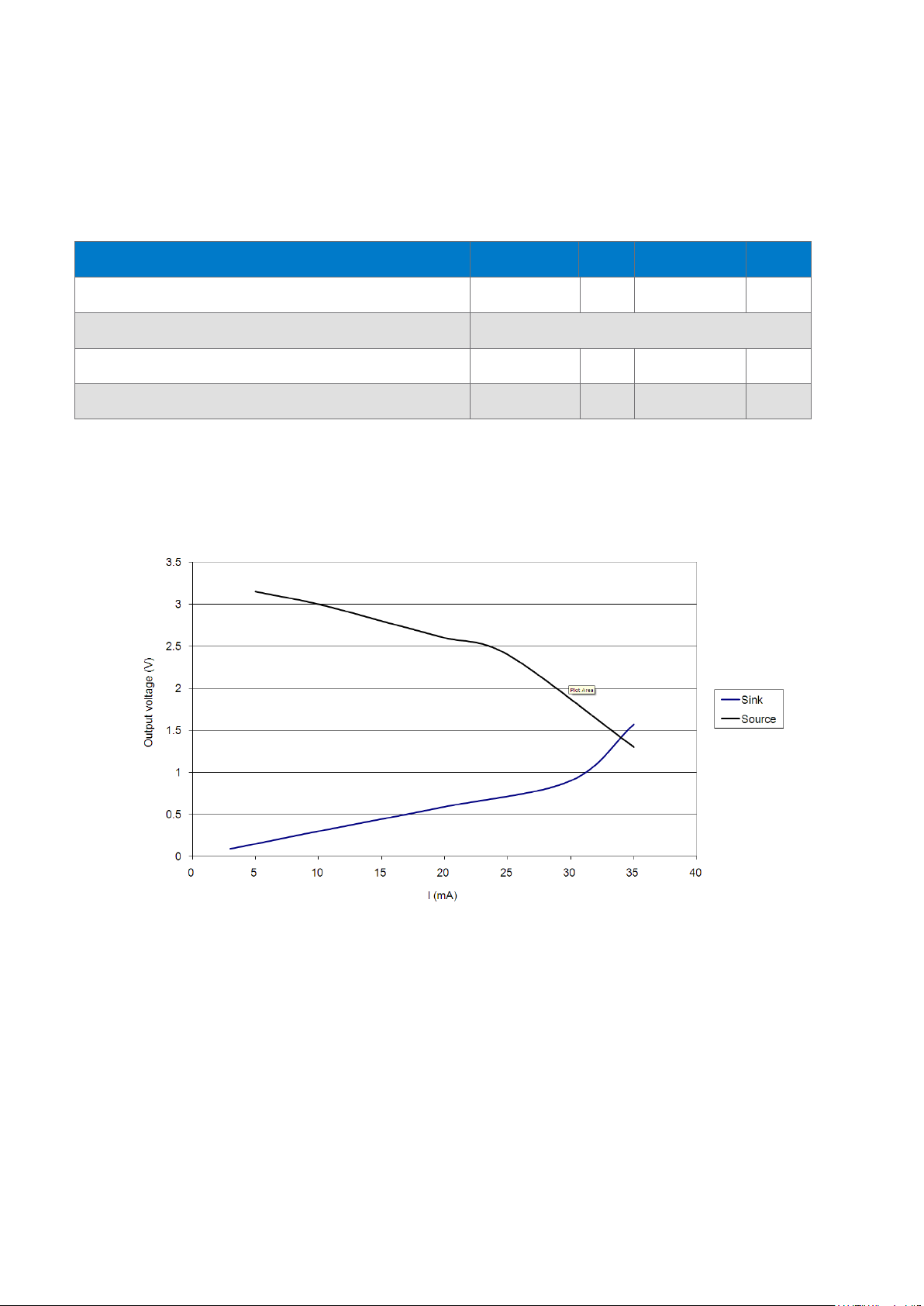
3.4 PIO Current Sink and Source Capability
Figure 2: WT41u PIO Current Drive Capability
Silicon Labs
Page 13 of 44

3.5 Transmitter Performance For BDR
RF characteristic Min Typ Max Blue to oth specification Unit
Max transmit power 16 17 18 <20 dBm
Transmit power variation over temperature
range
Transmit power variation over supply voltage
range
Transmit power variation over frequency
range
Transmit power control range -13 17 dBm
20dB bandwidth for modulated carrier 998 <1000 kHz
Avg drift -11 6 ±40 kHz
ΔF1avg 165 140 to 175 kHz
-2 2 dB
-0.5 0.5 dB
-0.5 0.5 dB
Silicon Labs
Page 14 of 44

3.6 Receiver Performance
Antenna gain not taken into account
Characteristic, VDD=3.3V, room temperature Packet type Typ Bluetooth
Sensitivity for 0.1% BER
Sensitivity variation over temperature range +/-2 dB
3.7 Current Consumption
Unit
specification
DH1 -94.1 -70 dBm
DH5 -90.5 dBm
2-DH1 -96.5 dBm
2-DH5 -94.5 dBm
3-DH1 -89.5 dBm
3-DH5 -86 dBm
Table 10: Receiver sensitivity
Operating mode Peak Average Unit
Stand-by, page mode 0 2000 1 2 mA
TX 3-DH5 108 85 mA
TX 2-DH5 108 85 mA
TX DH5 184 136 mA
RX 50 44 mA
Deep sleep, page mode 0 2000 1 0.36 mA
Inquiry 113 58 mA
Table 11: Current consumption
Silicon Labs
Page 15 of 44

4 Physical Dimensions
Figure 3: Physical dimensions (top view)
Figure 4: Dimensions for the RF pin used as antenna connection on WT41u-N (top view)
Silicon Labs
Page 16 of 44

Figure 5: Dimensions of WT41u-E
Figure 6: Dimensions of WT41u-A
Silicon Labs
Page 17 of 44

Figure 7: Recommended land pattern
Silicon Labs
Page 18 of 44

5 Soldering Recommendations
This section describes the soldering recommendations regarding WT41u Module.
WT41u is compatible with industrial standard reflow profile for Pb-free solders. The reflow profile used is
dependent on the thermal mass of the entire populated PCB, heat transfer efficiency of the oven, and
particular type of solder paste used.
• Refer to technical documentations of particular solder paste for profile configurations.
• Avoid using more than two reflow cycles.
• Aperture size of the stencil should be 1:1 with the pad size.
• A no-clean, type-3 solder paste is recommended.
• For further recommendation, please refer to the JEDEC/IPC J-STD-020, IPC-SM-782 and IPC 7351
guidelines.
Silicon Labs
Page 19 of 44

Signals
GND
Power
Signals
Overlapping GND layers without
GND stitching vias
Overlapping GND layers with
GND stitching vias shielding the
RF energy
6 Layout Guidelin es
Use good layout practices to avoid excessive noise coupling to supply voltage traces or sensitive analog
signal traces, such as analog audio signa ls. If using overlapp ing ground planes use stitching vias se parated
by max 3 mm to avoid emission f rom the edges of the PC B. Connect all the G ND pins direc tly to a solid GND
plane and make s ure that ther e is a lo w impedanc e path for the r eturn cur rent f ollowing the s ignal an d supp ly
traces all the way from start to the end.
A good practice is to dedicate one of the inner layers to a solid GND plane and one of the inner layers t o
supply voltage planes and traces and route all the signals on top and bottom layers of the PCB. This
arrangement will m ake sure that an y return current fo llows the forward c urrent as close as possible and any
loops are minimized.
Figure 8: Typical 4-layer PCB construction
Figure 9: Use of stitching vias to avoid emissions from the edges of the PCB
Page 20 of 44
Silicon Labs

7 UART Interface
This is a standard UART interface for communicating with other serial devices.WT41u UART interface
provides a simple mechanism for communicating with other serial devices using the RS232 protocol.
Four signals are used to implement the UART function. When WT41u is connected to another digital device,
UART_RX and UART_TX transfer data between the two devices. The remaining two signals, UART_CTS and
UART_RTS, can be used to implement RS232 hardware flow control where both are active low indicators. All
UART connections are implemented using CMOS technology and have signalling levels of 0V and VDD.
UART configuration parameters, such as data rate and packet format, are set using WT41u software.
Note:
In order to commun icate with the U ART at its maximum da ta rate using a standa rd PC, an acc elerated seri al
port adapter card is required for the PC.
Parameter Possible values
Data rate Minimum 1200bps (2% error)
9600bps (1% error)
Maximum 3Mbps (1% error)
Flow control RTS/CTS or None
Parity None, Odd or Even
Number of stop bits 1 or 2
Bits per channel 8
Table 12: Possible UART Settings
The UART interface is capabl e of r esetti ng WT41u upon recept ion of a bre ak signal. A break is ide ntified b y a
continuous logic low (0 V) on the UART _RX terminal, as shown in Figure 10. If tBRK is longer than the value,
defined by PSKEY_HOST_IO_UART_RESET_TIMEOUT, (0x1a4), a reset will occur. This feature allows a
host to initialise the system to a known state. Also, WT41u can emit a break character that may be used to
wake the host.
Figure 10: Break Signal
Table 17 shows a list of commonly used data rates and their associated values for
PSKEY_UART _BAUD_RATE (0x2 04). There is no requirem ent to use these standard values. An y data rate
within the supported range can be set in the PS Key according to the formula in Equation 1.
Silicon Labs
Page 21 of 44

Equation 1: Data Rate
Data rate [bits/s] Persistent store value
Error [bits/s] Error [%]
(Hex)
1200 0x0005 5 1.73
2400 0x000A 10 1.73
4800 0x0014 20 1.73
9600 0x0027 39 -0.82
19200 0x004F 79 0.45
38400 0x009D 157 -0.18
57600 0x00EC 236 0.03
76800 0x013B 315 0.14
115200 0x01D8 472 0.03
230400 0x03B0 944 0.03
460800 0x075F 1887 -0.02
921600 0x0EBF 3775 0
1382400 0x161E 5662 -0.01
1843200 0x1D7E 7550 0
2764800 0x2C3D 11325 0
Table 13: Standard Data Rates
Silicon Labs
Page 22 of 44

7.1 UART Bypass
Figure 11: UART Bypass Architecture
7.2 UART Configuration While Reset is Active
The UART interface for WT41u while the chip is being held in reset is tr istate. T his will allow the user to dais y
chain devices onto the ph ysical UART bus. The constr aint on this method is that any devices c onnected to
this bus must tristate when WT41u reset is de-asserted and the firmware begins to run.
7.3 UART Bypass Mo de
Alternatively, for de vices that do not tristate the UART bus, the UART bypass mode on the chipset can be
used. The default state of the c hipset after reset is de-ass erted; this is for the hos t UART bus to be connec ted
to the chipset U ART, thereby allowing communication to the chipset via the UART. All UART bypass mode
connections are implemented using CMOS technology and have signalling levels of 0V and VDD.
In order to apply the UART bypass mode, a BCCMD command will be issued to the chipset. Upon this issue, it
will switch the bypass to P IO[7:4] as Figure 11 indica tes. Once the bypass mode has been invoked, WT41u
will enter the Deep Sleep state indefinitely.
In order to re-estab lish communication with WT41u, the chip m ust be reset so that the def ault configuration
takes effect.
It is important for the host to ensure a clean Bluetooth disconnection of a ny active links before the b ypass
mode is invoked. Therefore, it is not possible to have active Bluetooth links while operating the bypass mode.
The current consum ption for a device in UART bypass mode is equal to t he values quoted for a device in
standby mode.
Silicon Labs
Page 23 of 44

8 USB Interface
This is a full speed (12Mbit s/s ) USB interf ace f or comm unicating with other com patible dig ital de vices. WT41u
acts as a USB peripheral, responding to requests from a master host controller such as a PC.
The USB interface is capa ble of driving a USB cable directl y. No external USB transceiver is r equired. The
device operates as a U SB peripheral, responding to requests from a master host controller such as a PC.
Both the OHCI and the UHCI standards are supported. The set of USB endpoints implemented can behave as
specified in the USB sec tion of the Blue tooth v2.1 + EDR specificat ion or alternat ively can appe ar as a set of
endpoints appropriate to USB audio devices such as speak er s .
As USB is a master/slave oriented system (in common with other USB peripherals), WT41u only supports
USB Slave operation.
8.1 USB Data Connections
The USB data lines em erge as pins USB_DP and USB_DN. These term inals are connected to the internal
USB I/O buffers of the the c hipset, therefore, have a low output impedance. To matc h the connection to the
characteristic impedance of the U SB c ab le, res ist ors m us t be p laced in series with US B_D P/U SB _DN and the
cable.
8.2 USB Pull-Up resistor
WT41u features an internal USB pull-up resistor. This pulls the USB_DP pin weakly high when WT41u is
ready to enumerate. It signals to the PC that it is a full speed (12Mbits/s) USB device.
The USB internal pu ll-up is implem ented as a current source, and is compliant with section 7.1.5 of the USB
specification v1.2. T he internal pull-up pulls USB_D P high to at least 2.8V when loaded with a 15kΩ 5% pulldown resistor (in the hub/h ost) when VDD_PADS = 3.1V. T his presents a Thevenin resista nce to the host of
at least 900Ω. Alternati vely, an external 1.5kΩ pull-up resistor can be placed be tween a PIO line and D+ on
the USB cable. T he firmware must be alerted to whic h mode is used by s etting PSKEY_US B_PIO_PULLUP
appropriately. The default setting uses the internal pull-up resistor.
8.3 USB Power Supply
The USB specificatio n dictates that the minimum output h igh voltage for USB data lines is 2.8 V. To safely
meet the USB specification , the voltage on the VDD supply terminal must be an absolute minimum of 3.1V.
Silicon Labs recommends 3.3V for optimal USB signal quality.
8.4 Self-Powered Mode
In self-powered mode, the circuit is powered from its own power supply and not from the VBUS (5V) line of the
USB cable. It draws only a small leakage current (below 0.5mA) from VBUS on the USB cable. This is the
easier mode for wh ich to design, as the des ign is not limited by the power that can be dra wn from the USB
hub or root port. However, it requires that VBUS be connected to WT41u via a resistor network (R
), so WT41u can detect when VBUS is powered u p. T he chipset will not pull USB_DP high when VBUS is
R
vb2
off.
vb1
and
Self-powered USB designs (powered f rom a batter y or PSU) must ens ure that a PIO line is a llocated f or USB
pullup purposes. A 1. 5kΩ 5% pull-up resis tor between USB_D P and the selecte d PIO line sho uld be fitted t o
the design. Failure to fit this resistor may result in the design failing to be USB compliant in self-powered
mode. The internal pull-up in the chipset is only suitable for bus-powered USB devices, e.g., dongles.
Silicon Labs
Page 24 of 44

Figure 12: USB Connections for Self-Powered Mode
The terminal mark ed USB_ON can be any free PIO pin. The PIO pi n selected must be registered b y setting
PSKEY_USB_PIO_VBUS to the corresponding pin number.
Identifier Value Function
Rs 27Ω nominal Impedance matching to USB cable
R
22kΩ 5% VBUS ON sense divider
vb1
R
47kΩ 5% VBUS ON sense divider
vb2
Figure 13: USB Interface Component Values
8.5 Bus-Powered Mode
In bus-powered m ode, the application circuit dra ws its current from the 5V VBU S supply on the USB cabl e.
WT41u negot iates with the PC during the US B enumeration stage about ho w much current it is allowed to
consume. O n power-up the device must not draw more than 100 m A but af ter being conf igured it c an dra w up
to 500 mA.
For WT41u, the USB power descriptor should be altered to reflect the amount of power required. This is
accomplished by setti ng PSKEY_USB_MAX_POWER (0x2c6) . This is higher than for a Class 2 applicat ion
due to the extra current drawn by the Transmit RF PA. By default for WT41u the setting is 300 mA.
When selecting a re gulator, be awar e that VBUS m ay go as low as 4.4V. The inrus h current (when charging
reservoir and suppl y decoupling capacitors) is limited by the USB s pecification. See the USB Specification.
Some applications m ay require sof t start c ircuitry to li mit inrush cur rent if m ore than 10uF is present between
VBUS and GND. The 5V V BUS lin e emerging from a PC is of ten e lec tric al ly noisy. As well as regulation dow n
to 3.3V and 1.8V, applications should include careful filtering of the 5V line to attenuate noise that is above the
voltage regulator bandw idth. Excessive nois e on WT41u supply pins will result i n reduced receiver sensitivity
and a distorted RF transmit signal.
Silicon Labs
Page 25 of 44

Figure 14: USB Connections for Bus-Po wered Mode
8.6 USB Suspend Current
All USB devices must permit the USB controller to place them in a USB suspend mode. While in USB
Suspend, bus-powered dev ices m ust not dra w more th an 2.5m A from USB VBU S (se lf-powered devices m ay
draw more than 2.5mA fr om their own su pply). This c urrent draw r equirement pr events operat ion of the r adio
by bus-powered devices during USB Suspend.
When computing suspend current, the current from VBUS through the bus pull-up and pull-down resistors
must be included. The pu ll-up resistor at t he device is 1.5 k Ω. (nominal). The pul l-down resistor at th e hub is
14.25kΩ. to 24.80kΩ. The pull-up voltage is nominall y 3.3V, which means that holding o ne of the signal lines
high takes approximately 200uA, leaving only 2.3mA available from a 2.5mA budget. Ensure that external
LEDs and/or amplifiers can be turned off by the chipset. The entire circuit m ust be able to enter the s uspend
mode.
8.7 USB Detach and Wake-Up Signaling
WT41u can provide out-of-band signa ling to a host controller b y using the control lines cal led USB_DETACH
and USB_WAKE_UP. These are outside the USB specification (no w ires exis t f or t hem inside the USB cable) ,
but can be useful when embedding WT41u into a circuit where no extern al USB is visible t o the user. Both
control lines are shared with PIO pins and can be assigned to any PIO pin by setting
PSKEY_USB_PIO_DETACH and PSKEY_USB_PIO_WAKEUP to the selected PIO number.
USB_DETACH is an i nput which, when assert ed high, causes WT41u to put USB_DN an d USB_DP in high
impedance state and turns off the pull-up resistor on DP. This detaches the device from the bus and is
logically equivalent t o unplugging the dev ice. When USB_DET ACH is taken low, WT41u will connect back to
USB and await enumeration by the USB host.
USB_WAKE_UP is an active high out put (used only when U SB_DETACH is ac tive) to wak e up the host a nd
allow USB comm unication to recom mence. It repl aces the functi on of the soft ware USB W AKE_UP mes sage
(which runs over the USB cable) an d cannot be sent while the chipset is effectively disconnected from the
bus.
Silicon Labs
Page 26 of 44

Figure 15: USB_Detach and USB_Wake_Up Signals
8.8 USB Driver
A USB Bluetooth device dr iver is required to provide a software interface betwe en the chipset and Bluetoo th
software running on the host computer. Please, contact Silicon Labs support at http://www.silabs.com
suitable drivers.
for
8.9 USB v2.0 Compliance and Compatibility
Although WT41u meets the USB specification, Silicon Labs cannot guarantee that an application circuit
designed around the m odule is USB com pliant. The choic e of applicat ion circuit, component c hoice and PC B
layout all affect USB sig nal quality and e lectrical char acteristics. T he inform ation in this document is intended
as a guide and should be read in assoc iation with the USB spec ification, with part icular attention being gi ven
to Chapter 7. Independent USB qual ification must be sought bef ore an applicatio n is deemed USB complian t
and can bear the US B logo. Such qua lification can be obtained f rom a USB plugf est or from an in dependent
USB test house.
Terminals USB_DP and USB_DN adhere to the USB Specification v2.0 (Chapter 7) electrical requirements.
The chipset is compatible with U SB v2.0 host contr ollers; under thes e circumstances the t wo ends agree the
mutually acceptable rate of 12Mbits/s according to the USB v2.0 specification.
Silicon Labs
Page 27 of 44

9 Serial Peripheral Interface (SPI)
The SPI port can be us ed for system debugg ing. It can also be used for programm ing the Flash m emory and
setting the PSKEY configurations. WT41u uses 16-bit d ata a nd 1 6-bit address serial per ip hera l in terface, where
transactions may occur wh en the interna l processor is running or is s topped. SPI interface is c onnected usin g
the MOSI, MISO, CS B and CLK pins. Please, contact the Silicon Labs support at http://www.silabs.com
detailed information about the instruction cycle.
for
Silicon Labs
Page 28 of 44

10 PCM Codec Interface
PCM is a standard method used to digitize audio (particularly voice) for transmission over digital
communication chann els. T hrough its PCM int erfac e, WT41u has hardware sup port f or c ontinual trans m ission
and reception of PCM data, thus reducing processor overhead for wireless headset applications. WT41u
offers a bidirection al digi tal aud io int er f ac e that r out es directly into the baseband la yer of the on-chip firmware.
It does not pass through the HCI protocol layer.
Hardware on WT41u allows the data to be sent to and received f rom a SCO connection. Up to t hree SCO
connections can be supported by the PCM interface at any one time.
WT41u can operate as the PCM interface master generating a n output clock of 128, 256 or 512kHz. When
configured as PCM interface slave, it can operate with an input clock up to 20 48kHz. WT41u is compatible
with a variety of clock formats, including Long Frame Sync, Short Frame Sync and GCI timing environments.
It supports 13-bit or 16-bit linear, 8-bit µ-law or A-law companded sam ple formats at 8ksamples/s and can
receive and transmit on any selection of three of the first four slots following PCM_SYNC. The PCM
configuration options are enab led b y setting PS K EY_ PCM_CONFIG32.
WT41u interfaces directly to PCM audio devices.
NOTE: Analog audio lines are very sensitive to RF disturbance. Use g ood layout practices to ensure noise
less audio. Make sure that the r eturn path for the audio signals fo llow s t he forw ar d c ur rent all th e way as clos e
as possible and use fully differential signals when possible. Do not compromise audio routing.
10.1 PCM Interface Master/Slave
When configured as the master of the PCM interface, WT41u generates PCM_CLK and PCM_SYNC.
Figure 16: PCM Interface Master
When configured as the Slave of the PCM interface, WT41u accepts PCM_CLK rates up to 2048kHz.
Silicon Labs
Page 29 of 44

10.2 Long Frame Sync
Figure 17: PCM Interface Slave
Long Frame Sync is the name given to a clocking format that controls the transfer of PCM data words or
samples. In Long Frame Sync, the rising edge of PCM_SYNC indicates the start of the PCM word. When
WT41u is configured as PCM master, generating PCM_SYNC and PCM_CLK, then PCM_SYNC is 8-bits
long. W hen WT41u is conf igured as PCM Slave, PCM_S YNC may be from two consec utive falling edges of
PCM_CLK to half the PCM_SYNC rate, i.e., 62.5s long.
Figure 18: Long Frame Sync (Shown with 8-bit Companded Sample)
WT41u samples PCM_IN on the falling edge of PCM_CLK and transmits PCM_OUT on the rising edge.
PCM_OUT may be configur ed to be high impedance on the fallin g edge of PCM_CLK in the LSB posit ion or
on the rising edge.
10.3 Short Frame Sync
In Short Frame Sync, the falling edge of PCM_SYNC indicates the start of the PCM word. PCM_SYNC is
always one clock cycle long.
Silicon Labs
Page 30 of 44

Figure 19: Short Frame Sync (Shown with 16-bit Sample)
As with Long Frame Sync, WT41u samples PCM_IN on the falling edge of PCM_CLK and transmits
PCM_OUT on the ris ing edge. PCM_OUT may be conf igured to be high impedance on the falling edge of
PCM_CLK in the LSB position or on the rising edge.
10.4 Multi-slot Operation
More than one SCO c onnection over the PCM interf ace is supported using multi ple slots. Up to three SCO
connections can be carried over any of the first four slots.
Figure 20: Multi-slot Operation with Two Slots and 8-bit Companded Samples
10.5 GCI Interface
WT41u is com patible with the GCI, a standar d sync hronous 2B +D ISDN tim ing i nterface. T he two 64k bits/s B
channels can be accessed when this mode is configured.
Silicon Labs
Page 31 of 44

Figure 21: GCI Interface
The start of fram e is indicated by the rising edge of PCM_SYNC and runs at 8k Hz. With WT41u in Slave
mode, the frequency of PCM_CLK can be up to 4.096MHz.
10.6 Slots and Sample Formats
WT41u can receive and transmit on any selection of the first four slots following each sync pulse. Slot
durations can be either 8 or 16 c lock cycles. Durations of 8 clock cycles may only be used with 8-bit s ample
formats. Durations of 16 clocks may be used with 8-bit, 13-bit or 16-bit sample formats.
WT41u supports 13-bit linear, 16-bit linear and 8-bit -law or A-law sample formats. The sample rate is
8ksamples/s. The bit order may be little or big endian. W hen 16-bit slots are used, the 3 or 8 unused bits in
each slot may be filled with sign extension, padded with zeros or a programmable 3-bit audio attenuation
compatible with some Motorola codecs.
Silicon Labs
Page 32 of 44

Figure 22: 16-bit Slot Length and Sample Formats
10.7 Additional Features
WT41u has a mute f acility that f orces PCM_OUT to be 0. In m as ter mode, PCM_S YNC m a y also be forced to
0 while keeping PCM_CLK running which some codecs use to control power down.
10.8 PCM_CLK and PCM_SYNC Generation
WT41u has two m ethods of generating PCM_CL K and PCM_SYNC in mas ter mode. The first is generating
these signals by DD S from the chipset interna l 4MHz clock. Using this mode limits PCM_CLK to 128, 25 6 or
512kHz and PCM_SYNC to 8kHz. The second is generating PCM_C LK and PCM_SYNC by DDS from an
internal 48MHz clock (which allows a greater range of frequencies to be generated with low jitter but
consumes more power). This second method is selected by setting bit 48M_PCM_CLK_GEN_EN in
PSKEY_PCM_CONFIG3 2. When in this mode and with long fram e sync, the length of PCM_S YNC can be
either 8 or 16 cycles of PCM_CLK, determined by LONG_LENGTH_SYNC_EN in PSKEY_PCM_CONFIG32.
The Equation 2 describes PCM_CLK frequency when being generated using the internal 48MHz clock:
Silicon Labs
Page 33 of 44

Equation 2: PCM_CLK Frequency When Being Generated Using the Internal 48MHz Clock
The frequency of PCM_SYNC relative to PCM_CLK can be set using Equation 3:
Equation 3: PCM_SYNC Frequency Relative to PCM_CLK
CNT_RATE, CNT_LIMIT and SYNC_LIMIT are set using PSKEY_PCM_LOW_JITTER_CONFIG. As an
example, to generate PCM_CLK at 512kHz with PCM_SYNC at 8kHz, set
PSKEY_PCM_LOW_JITTER_CONFIG to 0x08080177.
10.9 PCM Configuration
The PCM configuration is set using two PS Keys, PSKEY_PCM_CONFIG32 detailed in Table 18 and
PSKEY_PCM_LOW _JITT ER_CONFIG in Tabl e 19. Th e default f or P SKEY_PC M_CO NFIG 32 is 0x 008000 00,
i.e., first slot following sync is active, 13-bit linear voice format, long frame sync and interface master
generating 256kHz PCM_CLK from 4MHz internal clock with no tri-state of PCM_OUT.
Silicon Labs
Page 34 of 44

Name Bit
Description
position
- 0 Set to 0
SLAVE MODE EN 1 0 selects Master mode with internal generation of PCM_CLK and
PCM_SYNC. 1 selects Slave mode requiring externally generated
PCM_CLK and PCM_SYNC. This should be set to 1 if
48M_PCM_CLK_GEN_EN (bit 11) is set.
SHORT SYNC EN 2 0 selects long frame sync (rising edge indicates start of frame),
- 3 Set to 0
SIGN EXTENDED
EN
4 0 selects long frame sync (rising edge indicates start of frame), 1 selects
short frame sync (falling edge indicates start of frame).
LSB FIRST EN 5 0 transmits and receives voice samples MSB first, 1 uses LSB
TX TRISTATE EN 6 0 transmits and receives voice samples MSB first, 1 uses LSB
TX TRISTATE
RISING EDGE EN
7 0 tristates PCM_OUT immediately after the falling edge of PCM_CLK in the
last bit of an active slot, assuming the next slot is also not active. 1 tristates
PCM_OUT after the rising edge of PCM_CLK.
SYNC SUPPRESS
EN
8 0 enables PCM_SYNC output when master, 1 suppresses PCM_SYNC
whilst keeping PCM_CLK running. Some CODECS utilize this to enter a
low power state
GCI MODE EN 9 1 enables GCI mode.
MUTE EN 10 1 forces PCM_OUT to 0.
48M PCM CLK GEN
EN
11 0 sets PCM_CLK and PCM_SYNC generation via DDS from internal 4
MHz clock. 1 sets PCM_CLK and PCM_SYNC generation via DDS from
internal 48 MHz clock.
LONG LENGTH
SYNC EN
12 0 sets PCM_SYNC length to 8 PCM_CLK cycles and 1 sets length to 16
PCM_CLK cycles. Only applies for long frame sync and with
48M_PCM_CLK_GEN_EN set to 1.
- [20:16] Set to 0b00000.
MASTER CLK RATE [22:21] Selects 128 (0b01), 256 (0b00), 512 (0b10) kHz PCM_CLK frequency
when master and 48M_PCM_CLK_GEN_EN (bit 11) is low.
ACTIVE SLOT [26:23] Default is 0001. Ignored by firmaware
SAMPLE FORMAT [28:27] Selects between 13 (0b00), 16 (0b01), 8 (0b10) bit sample with 16 cycle
slot duration 8 (0b11) bit sample 8 cycle slot duration.
Table 14: PSKEY_PCM_CONFIG32 description
Silicon Labs
Page 35 of 44

Name Bit position Description
CNT LIMIT [12:0] Sets PCM_CLK counter limit
CNT RATE [23:16] Sets PCM_CLK count rate
SYNC LIMIT [31:24] Sets PCM_SYNC division relative to PCM_CLK
Table 15: PSKEY_PCM_LOW_JITTER_CONFIG Description
Silicon Labs
Page 36 of 44

11 I/O Parallel Ports
Six lines of programmable bidirectional input/outputs (I/O) are provided. All the PIO lines are power from VDD.
PIO lines can be c onfigured through software to have either weak or strong pull-ups or pull-downs. All PI O
lines are configured as inputs with weak pull-downs at reset. Any of the PIO lines can be configured as
interrupt request lines or as wake-up lines from sleep modes.
WT41u has a general purpose analogue interface pin AIO[1]. This is used to access internal circuitry and
control signals. It may be configured to provide additional functionality.
Auxiliary functions available via AIO[1] includ e an 8-bit ADC and an 8-bit DAC. Typically the A DC is used for
battery voltage measurement. Signals selectable at this pin include the band gap reference voltage and a
variety of clock signals: 48, 24, 16, 8MHz and the XTAL cl ock frequency. When used with analogue sign als,
the voltage range is constrained by the analogue supply voltage internally to the module (1.8V). When
configured to drive out digital level signals (e.g., clocks), the output voltage lev el is determined by VDD.
11.1 PIO Defaults
Silicon Labs can not guarantee that these term inal functions remain the sam e. Refer to the software releas e
note for the implementation of these PIO lines, as they are firmware build-specific.
Silicon Labs
Page 37 of 44

12 Reset
WT41u may be reset from several sources: RESET pin, power on reset, a UART break character or via
software configured watc hdog timer. The RESET pin is an active lo w reset and is internally filtered using the
internal low frequenc y clock oscillator. A reset will be per formed between 1.5 and 4.0ms following RES ETB
being active. It is recommended that RESET be applied for a period greater than 5ms.
The power on reset occurs when the VDD_CORE supply internally to the m odule f alls below typically 1.5V
and is released when VDD _CORE rises above t ypically 1.6V. At res et the digital I/O pins ar e set to inputs for
bidirectional pins and outputs are tri-state.
The reset should be held active at power up until all the supply voltages have stabilized to ensure correct
operation of the internal f lash m emory. Foll owing f igure sho ws an example of a s imple pow er up reset circuit.
Time constant of the RC circuitry is set so that the supply voltage is safely stabilized before the reset
deactivates.
Figure 23: Example of a simple power on reset circuit.
Silicon Labs
Page 38 of 44

12.1 Pin States on Reset
Pad name State
PIO[7:2] Input, weak pull-down
PCM_OUT 3-state, weak pull-down
PCM_IN Input, weak pull-down
PCM_SYNC Input, weak pull-down
PCM_CLK Input, weak pull-down
UART_TX 3-state, weak pull-up
UART_RX Input, weak pull-down
UART_RTS 3-state, weak pull-up
UART_CTS Input, weak pull-down
USB+ Input, weak pull-down
USB- Input, weak pull-down
SPI_CSB Input, weak pull-down
SPI_CLK Input, weak pull-down
SPI_MOSI Input, weak pull-down
SPI_MISO 3-state, weak pull-down
AIO[1] Output, driving low
Table 16: Pin States on Reset
Silicon Labs
Page 39 of 44

13 Certifications
13.1 Bluetooth
The WT41u is Bluetooth qualified and the declaration ID is B015141 (QDID 22298)
13.2 FCC
This device complies with Part 15 of the FCC Rules. Operation is subject to the following two conditions:
1. This device may not cause harmful interference, and
2. This device must accept any interference received, including interference that may cause
undesirable operation.
Any changes or modifications not expressly approved by Silicon Labs could void the user’s authority to
operate the equipment.
FCC RF Radiation Exposure Statement:
This equipment com plies with FCC radiation exposure lim its set forth for an uncontrolled e nvironment. End
users must follow th e specific operating ins tructions for satisfying RF exposure compliance. T his transmitter
meets both portable and mobi le l im its as demonstrated in the RF Exposure Ana l ysis . This tr ansm itter m us t not
be co-located or operating in c onj unct ion w ith any other antenna or transm itter ex cept in acc ordance with FCC
multi-transmitter product pr ocedures . As long as the c ondition above is met, f urther trans mitter tes ting wil l not
be required. Howev er, the OEM integrator is s till responsible for testi ng their end-product for any additional
compliance requirements required with this module installed (for example, digital device emissions, PC
peripheral requirements, etc.).
OEM Responsibilities to comply with FCC Regulations
The WT41u Module has been certified for integration into products only by OEM integrators under the
following condition:
• The antenna(s) must be installed such that a minimum separation distance of 42 mm is
maintained between the radiator (antenna) and all persons at all times.
• The transmitter module must not be co-located or operating in conjunction with any other
antenna or transmitter except in accordance with FCC multi-transmitter product procedures.
As long as the conditio ns above are met, fur ther transmitter testing will no t be required. However, the O EM
integrator is still resp onsible f or testing their e nd-product f or any addition al compliance r equirements required
with this module installed (for example, digital device emissions, PC peripheral requirements, etc.).
Note: In the event that this condition cannot be met (for certain configurations or co-location with another
transmitter), then the FCC authorization is no longer c onsidered va lid and the FC C ID cannot be us ed on the
final product. In thes e circu m stances , the OEM i ntegr ator will be r espo nsible f or re-evaluating the end pr oduc t
(including the transmitter) and obtaining a separate FCC authorization.
End Product Labeling
The WT41u Mod ule is labeled with its o wn FCC ID. If the FCC ID is not visible when the m odule is installed
inside another de vice, then the outside of the device into which the m odule is installed m ust also display a
label referring to the enclosed module. In that case, the final end product must be labeled in a visible area with
the following:
"Contains Transmitter Module FCC ID: QOQWT41u"
or
"Contains FCC ID: QOQWT41u"
Silicon Labs
Page 40 of 44

The OEM integrator must not provide information to t he end user regardi ng how to install or remove this RF
module or change RF related parameters in the user manual of the end product.
13.3 ISEDC
This radio transmitter (IC: 5123A-WT41U) has been approved by Industry Canada to operate with the
embedded chip antenna. Other antenna types are strictly prohibited for use with this device.
This device complies with Industry Canada’s license-exempt RSS standards. Operation is subject to the
following two conditions:
1. This device may not cause interference; and
2. This device m ust ac cept an y inter ferenc e, inc luding inter ferenc e that m a y cause und esired operat ion
of the device.
RF Exposure Statement
Exception from routine SAR evaluation limits are given in RSS-102 Issue 5. WT41u meets the given
requirements when the m inimum separation dista nce to hum an body 40 mm. RF exposure or S AR evaluatio n
is not required whe n the separ ation dista nce is 40 mm or m ore. If the separ ation distance is less tha n 40 mm
the OEM integrator is responsible for evaluating the SAR.
OEM Responsibilities to c om pl y with IC Regu lations T he WT41u Module has bee n cer tified f or integr ation int o
products only by OEM integrators under the following conditions:
• The antenna(s) must be instal led such that a minimum separation distance of 40 mm is maintained
between the radiator (antenna) and all persons at all times.
• The transmitter m odule must not be co-located or operating in c onjunction wit h any other ante nna or
transmitter.
As long as the two conditions above are met, further transm itter testing will not be required. However, the
OEM integrator is still responsible for testing their end-product for any additional compliance requirements
required with this module installed (for example, digital device emissions, PC peripheral requirements, etc.).
Note: In the event that these c onditions cannot be m et (for certain configur ations or co-locatio n with another
transmitter), then the IC authorizatio n is no longer con sidered valid and t he IC ID cannot b e used on the final
product. In these circumstances, the OEM integrator will be responsible for re-evaluating the end product
(including the transmitter) and obtaining a separate IC authorization.
End Product Labeling
The WT41u module is labeled w ith its own IC ID. If the IC ID is not vis ible when t he module is ins talled ins ide
another device, then the outside of the device into which the module is installed must also display a label
referring to the e nclosed m odule. In that case, the f inal end pr oduct m ust be labeled in a visibl e area w ith th e
following:
"Contains Transmitter Module IC: 5123A-WT41u"
or
"Contains IC: 5123A-WT41u"
The OEM integrator has to be aware not to prov ide information to the end us er regarding how to install o r
remove this RF module or change RF related parameters in the user manual of the end product.
13.3.1 ISEDC (Français)
Cet émetteur radio (IC : 5 123A-WT41u) a reçu l'approbation d'Indus trie Canada pour une exploitation av ec
l'antenne puce incorporée. Il est strictement interdit d'utiliser d'autres types d'antenne avec cet appareil.
Silicon Labs
Page 41 of 44

Le présent appareil es t conforme aux CNR d’Industri e Canada applicables aux appareils radio exempts de
licence. L’exploitation est autorisée aux deux conditions suivantes:
1. L’appareil ne doit pas produire de brouillage; et
2. L’appareil doit accept er tout brouillage r adioélectr ique subi, m ême si le brouillage est s usceptible de
provoquer un fonctionnement non désiré de l’appareil.
Déclaration relative à l'exposition aux radiofréquences (RF)
Les limites applicables à l’exemption de l’évaluation c ourante du DAS sont énoncées dans l e CNR 102, 5e
édition. Le module Bluetooth WT41u répond aux exigences données quand la distance de séparation
minimum par rapport a u c o r ps humain est de 40 mm. L'évaluat ion de l'exposi tion aux RF ou du DAS n'est pas
requise quand la distance de séparation est de 40 mm ou plus. Si la distance de séparation est inférieure à 40
mm, il incombe à l'intégrateur FEO d'évaluer le DAS.
Responsabilités du FEO ayant trait à la conformité avec les règlements IC
Le Module Bluetooth WT41u a été certifié pour une intégration dans des produits uniquement par les
intégrateurs FEO dans les conditions suivantes:
• La ou les antennes do ivent être inst allées de te lle façon qu'une distance de séparation m inimum de 40 mm
soit maintenue entre le radiateur (antenne) et toute personne à tout moment.
• Le module émetteur ne d oit pas être install é au m êm e endroit ou f onctionner conjoin tem ent avec to ute au tre
antenne ou émetteur.
Dès lors que les deux con ditions ci-dessus sont r espectées, aucun test supplémentaire de l ’émetteur n’est
obligatoire. Cependa nt, il in com be toujo urs à l'intégra t eur FEO de tes ter la conf orm ité de son pro duit f inal vis à-vis de toute exigence supplémentaire requise avec ce module installé (par exemple, émissions de
dispositifs numériques, exigences relatives aux matériels périphériques PC, etc).
Note: S'il s'avère que ces conditions ne peuvent être respectées (pour certaines configurations ou la
colocation avec un autre émetteur), alors l'autorisation IC n'est plus cons i dér ée comme valide et l'identifiant IC
ne peut plus être emplo yé sur le produ it f inal . Dans c es c irc ons tanc es, l'intégr ate ur FEO aura la r esponsabilité
de réévaluer le produit final (y compris l'émetteur) et d'obtenir une autorisation IC distincte.
Étiquetage du produit final
L'étiquette du Module WT41u porte son propre identifiant IC. Si l'identifiant IC n'est pas visible quand le
module est installé à l'intérieur d'un autre appareil, alors l'extérieur de l'appareil dans lequel le module est
installé doit aus si porter une étiquette fais ant référence au module qu' il contient. Dans ce cas, un e étiquette
comportant les informations suivantes doit être apposée sur une partie visible du produit final.
"Contient le module émetteur IC: 5123A-WT41U"
ou
"Contient IC : 5123A-WT41U"
L'intégrateur FEO doit être conscient de ne pas fournir d'inf ormations à l'utilis ateur final perm ettant d'installer
ou de retirer ce module RF ou de changer les paramètres liés aux RF dans le mode d'emploi du produit final.
13.4 CE
The Declaration of Compliance and the test documentation can be consulted in www.silabs.com.
Please note that ever y application us ing the WT 41-A or WT41-N will need to perform the radio EMC tests on
the end product according to EN 301 489-17.
RF exposure requirements must be verified in an end product assembly.
Test documentation an d software for the EN 300 328 radi ated spurious emissions testin g can be requested
from the Silicon Labs support.
Silicon Labs
Page 42 of 44

13.5 MIC Japan
The WT 41u module in cer tified for Japan. Certification num ber: 209-J00231 Sin ce September 1, 2014 it is
allowed (and highl y rec om mended) that a manuf act urer who int egr at es a rad io module in their hos t e qu ipment
can place the certif ication m ark and certificatio n number (the sam e marking/nu mber as depict ed on the label
of the radio module) on the outside of the host equipment. The certification mark and certification number
must be placed cl ose to t he text in th e Jap anese lang uage which is pro vided b elo w. This c hange in th e R adio
Law has been made in order to enable users of the com bination of host and r adio m odule to verify if t hey are
actually using a radio device which is approved for use in Japan.
当該機器には電波法に基づく、技術基準適合証明等を受けた特定無線設備を装着している。
Translation: “This equipment contains specified radio equipment that has been certified to the Technical
Regulation Conformity Certification under the Radio Law.”
Silicon Labs
Page 43 of 44

13.6 Qualified Antenna Types for WT41u-E and WT41u-N
This device has been desig ned to oper ate with a stand ard 2.14 dBi dipole antenna. Any antenna of a diff erent
type or with a gain higher than 2. 14 dBi is strictly prohib ited for use with this device. Using an ante nna of a
different type or gain more than 2.14 dBi will require additional testing for FCC, CE and IC. The required
antenna impedance is 50 Ω.
Antenna type Maximum gain
Dipole 2.14 dBi
Table 17: Qualified Antenna Types for WT41u-E/N
To reduce potential radio inter ference to other users, t he antenna type and its gain shou ld be so chosen that
the equivalent isotropically radiated power (EIRP) is not more than that permitted for successful
communication.
Any standard 2.14 dBi dipole antenna can be used without an additional application to FCC.
13.7 Moisture Sensitivity Level (MSL)
Moisture sensitivit y level (MSL) of this product is 3. For the hand ling instructions please refer to JEDEC JSTD-020 and JEDEC J-STD-033.
If baking is required, devices may be baked for 12 hours at 125°C +/-5°C for high temperature device
containers.
Silicon Labs
Page 44 of 44

Simplicity Studio
One-click access to MCU and
wireless tools, documentation,
software, source code libraries &
more. Available for Windows,
Mac and Linux!
IoT Portfolio
www.silabs.com/IoT
Disclaimer
Silicon Labs intends to provide customers with the latest, accurate, and in-depth documentation of all peripherals and modules available for system and software implementers using or
intending to use the Silicon Labs products. Characterization data, available modules and peripherals, memory sizes and memory addresses refer to each specific device, and "Typical"
parameters provided can and do vary in different applications. Application examples described herein are for illustrative purposes only. Silicon Labs reserves the right to make changes
without further notice and limitation to product information, specifications, and descriptions herein, and does not give warranties as to the accuracy or completeness of the included
information. Silicon Labs shall have no liability for the consequences of use of the information supplied herein. This document does not imply or express copyright licenses granted
hereunder to design or fabricate any integrated circuits. The products are not designed or authorized to be used within any Life Support System without the specific written consent of
Silicon Labs. A "Life Support System" is any product or system intended to support or sustain life and/or health, which, if it fails, can be reasonably expected to result in significant personal
injury or death. Silicon Labs products are not designed or authorized for military applications. Silicon Labs products shall under no circumstances be used in weapons of mass
destruction including (but not limited to) nuclear, biological or chemical weapons, or missiles capable of delivering such weapons.
Trademark Information
Silicon Laboratories Inc.® , Silicon Laboratories®, Silicon Labs®, SiLabs® and the Silicon Labs logo®, Bluegiga®, Bluegiga Logo®, Clockbuilder®, CMEMS®, DSPLL®,
EFR, Ember®, Energy Micro, Energy Micro logo and combinations thereof, "the world’s most energy friendly microcontrollers", Ember®, EZLink®, EZRadio®, EZRadioPRO®,
Gecko®, ISOmodem®, Precision32®, ProSLIC®, Simplicity Studio®, SiPHY®, Telegesis, the Telegesis Logo®, USBXpress® and others are trademarks or registered trademarks of Silicon
Labs. ARM, CORTEX, Cortex-M3 and THUMB are trademarks or registered trademarks of ARM Holdings. Keil is a registered trademark of ARM Limited. All other products or brand
names mentioned herein are trademarks of their respective holders.
Silicon Laboratories Inc.
400 West Cesar Chavez
Austin, TX 78701
USA
SW/HW
www.silabs.com/simplicity
Quality
www.silabs.com/quality
Support and Community
community.silabs.com
EFM®, EFM32®,
http://www.silabs.com
 Loading...