

Silicon Laboratories Finland WT11U Users Manual

WT11u
DATA SHEET
Monday, 21 November 2016
Version 0.9.2

VERSION HISTORY
Version
Comment
0.8
Initial versions
0.81
Ordering information updated
0.9
Reformatted tables, many WT11i->WT11u updates
0.9.1
Rest of tables reformatted
0.9.2
Updated dimension drawings
Silicon Laboratories Finland Oy

TABLE OF CONTENTS
1 Ordering Information......................................................................................................................................6
2 Pinout and Terminal Description ...................................................................................................................7
3 Electrical Characteristics ............................................................................................................................ 10
3.1 Absolute Maximum Ratings ................................................................................................................ 10
3.2 Recommended Operating Conditions ................................................................................................. 10
3.3 Input / Output Terminal Characteristics .............................................................................................. 11
3.3.1 Input/Output Terminal Characteristics (Digital) ............................................................................ 11
3.3.2 Input/Output Terminal Characteristics (USB) .............................................................................. 12
3.4 PIO Current Sink and Source Capability ............................................................................................. 13
3.5 Transmitter Performance For BDR ..................................................................................................... 14
3.6 Receiver Performance ........................................................................................................................ 14
3.7 Current Consumption .......................................................................................................................... 15
3.8 WT11u-A Antenna Specification ......................................................................................................... 16
4 Physical Dimensions .................................................................................................................................. 19
4.1 Package Drawings .............................................................................................................................. 21
5 Layout Guidelines ....................................................................................................................................... 23
6 UART Interface ........................................................................................................................................... 26
6.1 UART Bypass ...................................................................................................................................... 28
6.2 UART Configuration While Reset is Active ......................................................................................... 28
6.3 UART Bypass Mode ............................................................................................................................ 28
7 USB Interface ............................................................................................................................................. 29
7.1 USB Data Connections ....................................................................................................................... 29
7.2 USB Pull-Up resistor ........................................................................................................................... 29
7.3 USB Power Supply .............................................................................................................................. 29
7.4 Self-Powered Mode ............................................................................................................................. 29
7.5 Bus-Powered Mode ............................................................................................................................. 30
7.6 USB Suspend Current ......................................................................................................................... 31
7.7 USB Detach and Wake-Up Signaling.................................................................................................. 31
7.8 USB Driver .......................................................................................................................................... 32
7.9 USB v2.0 Compliance and Compatibility ............................................................................................ 32
8 Serial Peripheral Interface (SPI) ................................................................................................................. 33
9 PCM Codec Interface ................................................................................................................................. 34
9.1 PCM Interface Master/Slave ............................................................................................................... 34
9.2 Long Frame Sync ................................................................................................................................ 35
9.3 Short Frame Sync ............................................................................................................................... 35
9.4 Multi-slot Operation ............................................................................................................................. 36
9.5 GCI Interface ....................................................................................................................................... 36
Silicon Laboratories Finland Oy

9.6 Slots and Sample Formats .................................................................................................................. 37
9.7 Additional Features ............................................................................................................................. 38
9.8 PCM_CLK and PCM_SYNC Generation ............................................................................................ 38
9.9 PCM Configuration .............................................................................................................................. 39
10 I/O Parallel Ports ..................................................................................................................................... 42
10.1 PIO Defaults ................................................................................................................................. 42
11 Reset ....................................................................................................................................................... 43
11.1 Pin States on Reset ..................................................................................................................... 44
12 Certifications ........................................................................................................................................... 45
12.1 Bluetooth ...................................................................................................................................... 45
12.2 FCC and IC .................................................................................... Error! Bookmark not defined.
12.2.1 FCC et IC ....................................................................................... Error! Bookmark not defined.
12.3 CE ................................................................................................................................................ 48
12.4 MIC Japan .................................................................................................................................... 48
12.5 KCC (Korea)................................................................................................................................. 48
12.6 Anatel ........................................................................................................................................... 49
12.7 Qualified Antenna Types for WT11u-E ........................................................................................ 50
12.8 Moisture Sensitivity Level (MSL).................................................................................................. 50
Silicon Laboratories Finland Oy
WT11u Bluetooth® Module
DESCRIPTION
WT11u is a fully integrated Bluetooth 2.1 +
EDR, class 1 module combining
antenna, Bluetooth radio and an on-board
iWRAP Bluetooth stack. Silicon Labs WT11u
provides an ideal solution for developers that
want to quickly integrate long range and
high performance Bluetooth wireless
technology to their design without
investing several months into Bluetooth radio
and stack development. WT11u provides a
100dB link budget ensuring long rage and
robust Bluetooth connectivity. WT11u uses
Silicon Labs’ iWRAP Bluetooth stack, which is
an embedded Bluetooth stack implementing
13 different Bluetooth profiles and Apple iAP
connectivity. By using WT11u combined with
iWRAP Bluetooth stack and Silicon Labs’
excellent technical support designers ensure
quick time to market, low development costs
and risk.
APPLICATIONS:
Industrial and M2M
Point-of-Sale devices
Computer Accessories
KEY FEATURES:
Radio features:
Bluetooth v.2.1 + EDR
Bluetooth class 1 radio
Transmit power: +17 dBm
Receiver sensitivity: -84 dBm (DH5)
Range: 350 meters line-of-sight
Integrated chip antenna or U.FL
connector
Hardware features:
UART and USB host interfaces
802.11 co-existence interface
6 software programmable IO pins
Operating voltage: 2.7V to 3.6V
Temperature range: -40C to +85C
Dimensions: 35.75 x 14.50 x 2.6 mm
Qualifications:
Bluetooth
CE
FCC
IC
Japan
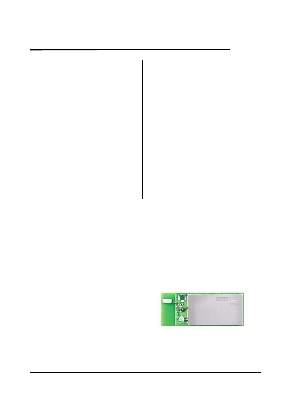
PHYSICAL OUTLOOK
Silicon Laboratories Finland Oy

1 Ordering Information
Firmware
U.FL Connector
Internal chip antenna
iWRAP 5.6 firmware, reel
WT11u-E-AI56
WT11u-A-AI56
iWRAP 5.5 firmware, reel
WT11u-E-AI55
WT11u-A-AI55
HCI firmware, BT2.1 + EDR, reel
WT11u-E-HCI21001
WT11u-A-HCI21001
iWRAP 5.6 firmware with iAP, reel
WT11u-E-AI56IAP
WT11u-A-AI56IAP
iWRAP 5.6 firmware, cut reel
WT11u-E-AI56C
WT11u-A-AI56C
iWRAP 5.5 firmware, cut reel
WT11u-E-AI55C
WT11u-A-AI55C
HCI firmware, BT2.1 + EDR, cut reel
WT11u-E-HCI21001C
WT11u-A-HCI21001C
iWRAP 5.6 firmware with iAP, cut reel
WT11u-E-AI56IAPC
WT11u-A-AI56IAPC
Table 1: Ordering information
Silicon Laboratories Finland Oy
Page 6 of 51
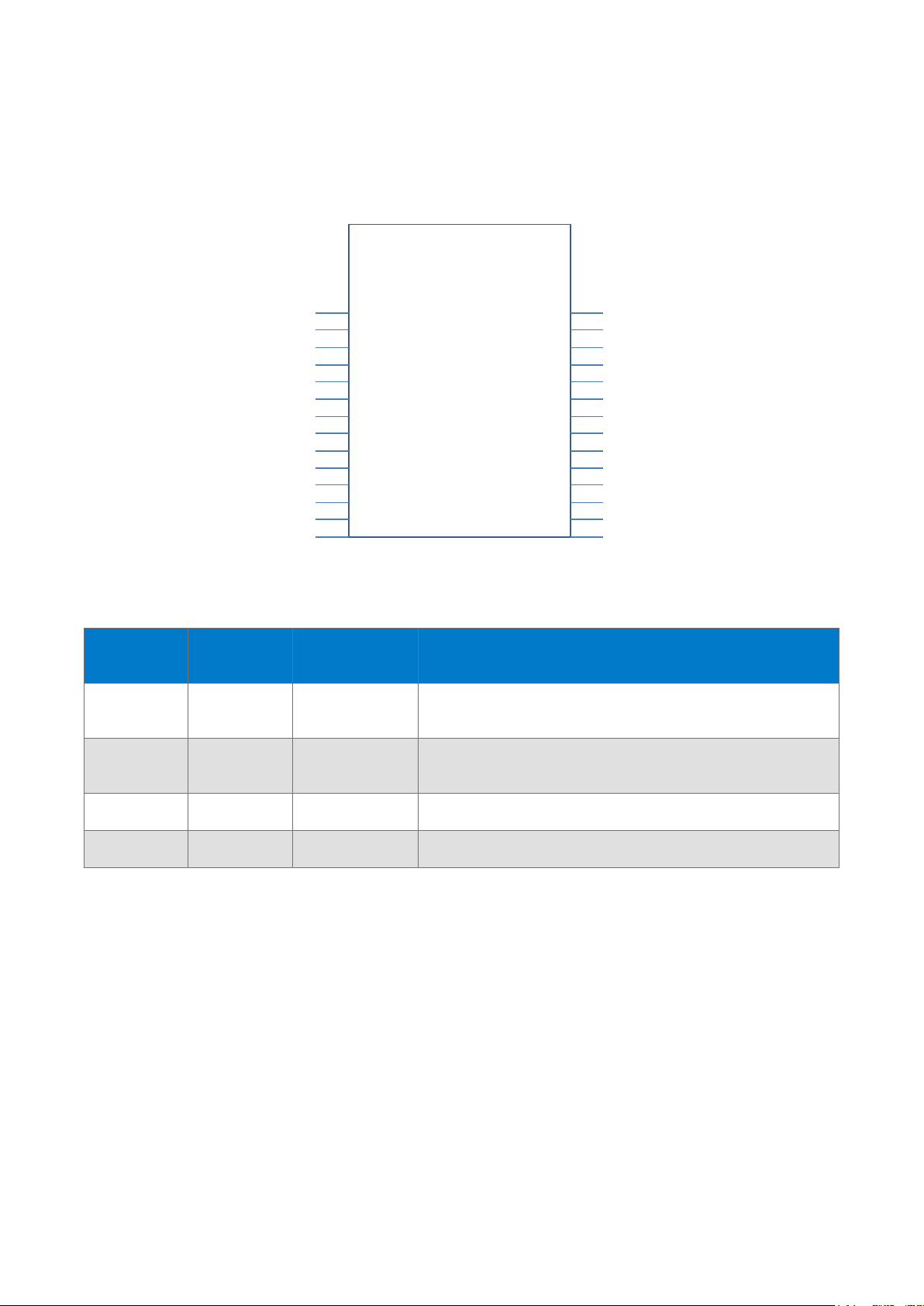
Pad name
Pad
number
Pad type
Description
RESET
17
Input
Reset input, active high, internal 220kohm pull-down. Keep
high for >5ms for reset
GND
1, 14, 15, 28
GND
Ground connection, connect all to a ground plane with
minimal trace lengths
VDD_PA
2
Supply voltage
Supply voltage for RF power amplifier
VDD
16
Supply voltage
Chipset supply voltage
WT11i
GND
VDD_PA
PIO2
PIO3
UART_RTS#
UART_RX
PCM_OUT
USB+
USB-
UART_CTS#
PCM_IN
PCM_CLK
PCM_SYNC
GND
GND
AIO
UART_TX
PIO5
SPI_MOSI
SPI_MISO
SPI_CLK
SPI_CS#
PIO4
PIO7
PIO6
RESET
VDD
GND
1
2
3
4
5
6
7
8
9
10
11
12
13
14
28
27
26
25
24
23
22
21
20
19
18
17
16
15
2 Pinout and Terminal Description
Figure 1: WT11u connection diagram
Table 2: Supply and RF Terminal Descriptions
Silicon Laboratories Finland Oy
Page 7 of 51
PIO signal
Pad number
Description
PIO[2]
3
Bi-directional digital in/out with programmable strength and pull-up/pulldown
PIO[3]
4
Bi-directional digital in/out with programmable strength and pull-up/pulldown
PIO[4]
20
Bi-directional digital in/out with programmable strength and pull-up/pulldown
PIO[5]
25
Bi-directional digital in/out with programmable strength and pull-up/pulldown
PIO[6]
18
Bi-directional digital in/out with programmable strength and pull-up/pulldown
PIO[7]
19
Bi-directional digital in/out with programmable strength and pull-up/pulldown
AIO[1]
27
Bi-directional analog in/out
PCM signal
Pad number
Pad type
Description
PCM_OUT
7
Output, weak internal pull-down
Synchronous data output
PCM_IN
11
Input, weak internal pull-down
Synchronous data input
PCM_SYNC
13
Bi-directional, weak internal pull-down
Synchronous data sync
PCM_CLK
12
Bi-directional, weak internal pull-down
Synchronous data clock
Table 3: GPIO Terminal Descriptions
Table 4: PCM Terminal Descriptions
Silicon Laboratories Finland Oy
Page 8 of 51
UART signal
Pad number
Pad type
Description
UART_TX
26
Output, weak internal
pull-up
UART data output, active
high
UART_RTS#
5
Output, weak internal
pull-up
UART request to send,
active low
UART_RX
6
Input, weak internal pulldown
UART data input, active
high
UART_CTS#
10
Input, weak internal pulldown
UART clear to send,
active low
USB signal
Pad number
Pad type
Description
USB+
8
Bidirectional
USB data line with internal 1.5kohm pull-up
USB-
9
Bidirectional
USB data line
SPI signal
Pad
number
Pad type
Description
SPI_MOSI
24
Input, weak internal pull-down
SPI data input
SPI_CS#
21
Input, weak internal pull-up
Chip select, active low
SPI_CLK
22
Input, weak internal pull-down
SPI clock
SPI_MISO
23
Output, weak internal pull-down
SPI data output
Table 5: UART Terminal Descriptions
Table 6: USB Terminal Descriptions
Table 7: Terminal Descriptions
Silicon Laboratories Finland Oy
Page 9 of 51
Specification
Min
Max
Unit
Storage temperature
-40
85
°C
VDD_PA, VDD
-0.4
3.6
V
Other terminal voltages
VSS-0.4
VDD+0.4
V
Specification
Min
Max
Unit
Operating temperature
-40
85
°C
VDD_PA*, VDD
3.0
3.6
V
3 Electrical Characteristics
3.1 Absolute Maximum Ratings
Table 8: Absolute Maximum Ratings
3.2 Recommended Operating Conditions
*) VDD_PA has an effect on the RF output power.
Table 9: Recommended Operating Conditions
Silicon Laboratories Finland Oy
Page 10 of 51

Digital Terminals
Min
Typ
Max
Unit
Input Voltage Levels
VIL input logic level low
2.7 V ≤ VDD ≤ 3.0 V
-0.4 - 0.8
V
1.7 V ≤ VDD ≤ 1.9 V
-0.4 - 0.4
V
VIH input logic level high
0.7 VDD
-
VDD + 0.4
V
Output Voltage Levels
VOL output logic level low
(IO = 4.0 mA) 2.7V ≤ VDD ≤ 3.0 V
- - 0.2
V
VOL output logic level low
(IO = 4.0 mA) 1.7V ≤ VDD ≤ 1.9
- - 0.4
V
VOL output logic level high
(IO = 4.0 mA) 2.7V ≤ VDD ≤ 3.0
VDD - 0.2
- V
VOL output logic level high
(IO = 4.0 mA) 1.7V ≤ VDD ≤ 1.9
VDD - 0.4
- V
Input and Tristate Current with
Strong pull-up
-100
-40
-10
µA
Strong pull-down
10
40
100
µA
Weak pull-up
-5.0
-1.0
-0.2
µA
Weak pull-down
0.2
1.0
5.0
µA
I/O pad leakage current
-1 0 1
µA
CI input capacitance
1.0 - 5.0
pF
3.3 Input / Output Terminal Characteristics
3.3.1 Input/Output Terminal Characteristics (Digital)
Silicon Laboratories Finland Oy
Page 11 of 51

USB Terminals
Min
Typ
Max
Unit
VDD_USB for correct USB operation
3.1 3.6
V
Input Threshold
VIL input logic level log
-
-
0.3VDD_USB
V
VIH input logic level high
0.7VDD_USB
- - V
3.3.2 Input/Output Terminal Characteristics (USB)
Silicon Laboratories Finland Oy
Page 12 of 51
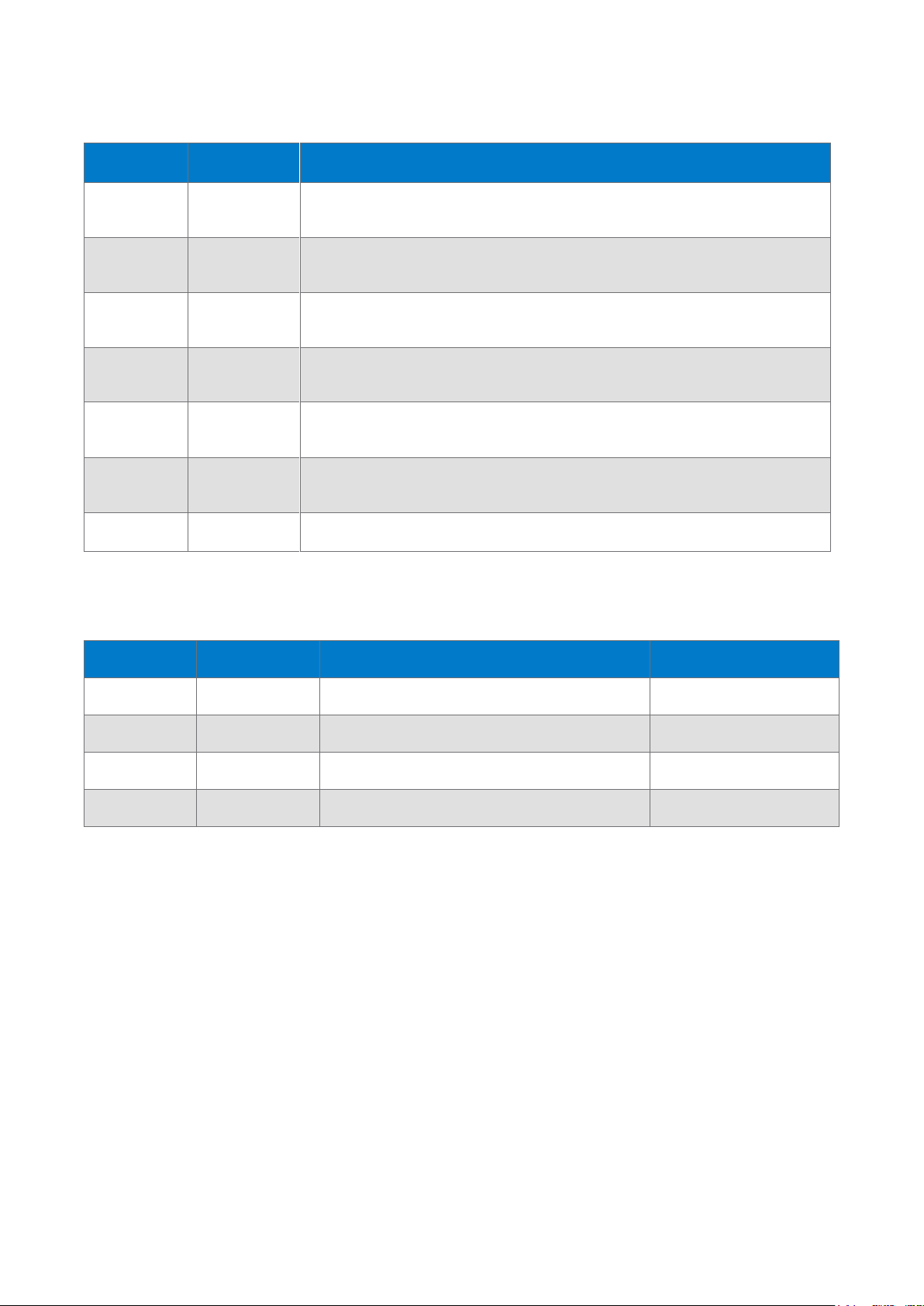
3.4 PIO Current Sink and Source Capability
Figure 2: WT11u PIO Current Drive Capability
Silicon Laboratories Finland Oy
Page 13 of 51
3.5 Transmitter Performance For BDR
RF characteristic
Min
Typ
Max
Bluetooth specification
Unit
Max transmit power
16
17
18.5
<20
dBm
Transmit power variation over temperature
range
TBD
dB
Transmit power variation over supply
voltage range
TBD
dB
Transmit power variation over frequency
range
TBD
dB
Transmit power control range
TBD 17 dB
20dB bandwidth for modulated carrier
TBD <1000
kHz
ACP
F = F0 ± 2MHz
TBD
-20
dBc
F = F0 ± 3MHz
TBD
-40
dBc
F = F0 > 3MHz
TBD
-40
dBc
Drift rate
TBD
±25
kHz
ΔF1avg
TBD 140 to 175
kHz
ΔF1max
TBD 140 to 175
kHz
ΔF2avg / ΔF1avg
TBD >=0.8
Table 10: Transmitter performance for BDR (room temperature, VDD=3.3V)
Figure 3: Typical TX power as a function of VDD_PA
3.6 Receiver Performance
Antenna gain not taken into account
TBD
Silicon Laboratories Finland Oy
Page 14 of 51
Characteristic, VDD=3.3V, room temperature
Packet type
Typ
Bluetooth
specification
Unit
Sensitivity for 0.1% BER
DH1
TBD
-70
dBm
DH5
-85
dBm
2-DH1
TBD
dBm
2-DH5
TBD
dBm
3-DH1
TBD
dBm
3-DH5
TBD
dBm
Sensitivity variation over temperature range
TBD
dBm
Operating mode
Peak
Average
Unit
Stand-by, page mode 0
TBD
mA
TX 3-DH5
TBD
mA
TX 2-DH5
TBD
mA
TX DH5
TBD
mA
RX
TBD
mA
Deep sleep
TBD
mA
Inquiry
TBD
mA
3.7 Current Consumption
Table 11: WT11u Current Consumption
Silicon Laboratories Finland Oy
Page 15 of 51
WT11i-A
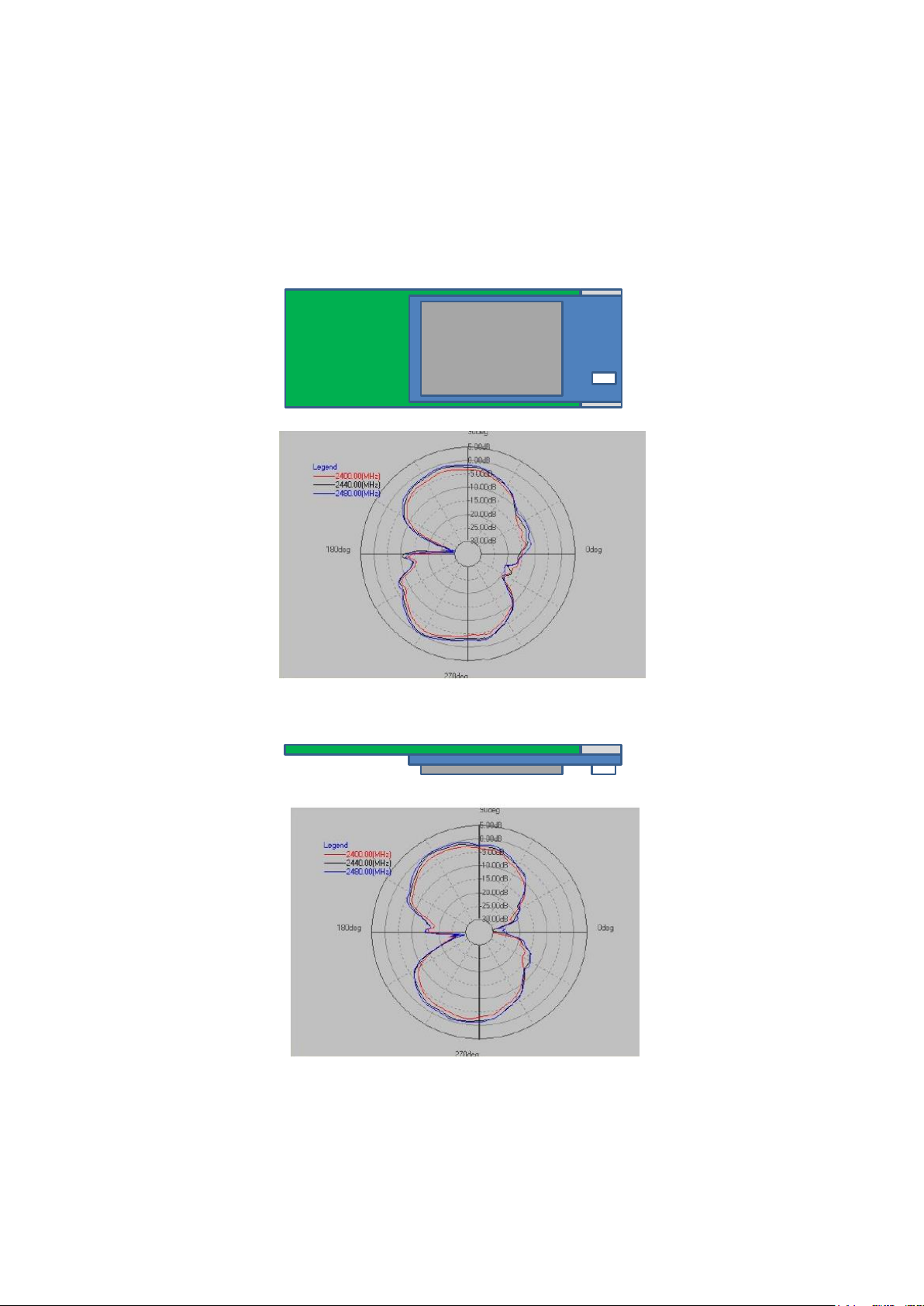
3.8 WT11u-A Antenna Specification
WT11u-A uses a monopole type on a chip antenna with maximum gain of 0.5 dBi. The radiation pattern and the
total radiated efficiency are dependent on the layout and any metal around the antenna has an effect on the
radiation characteristics. Typically the efficiency is 30 … 50%.
Figure 4: Antenna radiation pattern in a USB dongle layout
Figure 5: Antenna radiation pattern in a USB dongle layout
Silicon Laboratories Finland Oy
Page 16 of 51
 Loading...