


WT11i-E
DATA SHEET
Monday, 13 February 2012
Version 1.04

Copyright © 2000-2012 Bluegiga Technologies
All rights reserved.
Bluegiga Technologies assumes no responsibility for any errors which may appear in this manual.
Furthermore, Bluegiga Technologies reserves the right to alter the hardware, software, and/or specifications
detailed here at any time without notice and does not make any commitment to update the information
contained here. Bluegiga’s products are not authorized for use as critical components in life support devices
or systems.
The WRAP is a registered trademark of Bluegiga Technologies
The Bluetooth trademark is owned by the Bluetooth SIG Inc., USA and is licensed to Bluegiga Technologies.
All other trademarks listed herein are owned by their respective owners.
Bluegiga Technologies Oy

VERSION HISTORY
Version Comment
1.04 Typo corrections
1.03 Page 33: Reset is active high
1.02 Package drawings added
1.01 Ordering information corrected
1.0 Release
Bluegiga Technologies Oy

TABLE OF CONTENTS
1 Ordering Information..................................................................................................................................... 7
2 Pinout and Terminal Description .................................................................................................................. 8
3 Electrical Characteristics ............................................................................................................................ 11
3.1 Absolute Maximum Ratings ................................................................................................................ 11
3.2 Recommended Operating Conditions ................................................................................................. 11
3.3 Current Consumption .......................................................................................................................... 11
3.4 PIO Current Sink and Source Capability ............................................................................................. 12
3.5 Antenna Specification ......................................................................................................................... 12
4 Physical Dimensions .................................................................................................................................. 13
4.1 Package Dimensions .......................................................................................................................... 14
5 Layout Guidelines ....................................................................................................................................... 16
6 UART Interface ........................................................................................................................................... 17
6.1 UART Bypass ...................................................................................................................................... 19
6.2 UART Configuration While Reset is Active ......................................................................................... 19
6.3 UART Bypass Mode ............................................................................................................................ 19
7 USB Interface ............................................................................................................................................. 20
7.1 USB Data Connections ....................................................................................................................... 20
7.2 USB Pull-Up resistor ........................................................................................................................... 20
7.3 USB Power Supply .............................................................................................................................. 20
7.4 Self-Powered Mode ............................................................................................................................. 20
7.5 Bus-Powered Mode ............................................................................................................................. 21
7.6 USB Suspend Current ......................................................................................................................... 22
7.7 USB Detach and Wake-Up Signaling ................................................................................................. 22
7.8 USB Driver .......................................................................................................................................... 23
7.9 USB v2.0 Compliance and Compatibility ............................................................................................ 23
8 Serial Peripheral Interface (SPI) ................................................................................................................. 24
9 PCM Codec Interface ................................................................................................................................. 25
9.1 PCM Interface Master/Slave ............................................................................................................... 25
9.2 Long Frame Sync ................................................................................................................................ 26
9.3 Short Frame Sync ............................................................................................................................... 26
9.4 Multi-slot Operation ............................................................................................................................. 27
9.5 GCI Interface ....................................................................................................................................... 27
9.6 Slots and Sample Formats .................................................................................................................. 28
9.7 Additional Features ............................................................................................................................. 29
9.8 PCM_CLK and PCM_SYNC Generation ............................................................................................ 29
9.9 PCM Configuration .............................................................................................................................. 30
10 I/O Parallel Ports ..................................................................................................................................... 32
Bluegiga Technologies Oy

PIO Defaults ................................................................................................................................. 32
10.1
11 Reset ....................................................................................................................................................... 33
11.1 Pin States on Reset ..................................................................................................................... 33
12 Certifications ........................................................................................................................................... 34
12.1 Bluetooth ...................................................................................................................................... 34
12.2 FCC and IC .................................................................................................................................. 34
12.2.1 FCC et IC ..................................................................................................................................... 36
12.3 CE ................................................................................................................................................ 38
12.4 Qualified Antenna Types for WT11i-E ......................................................................................... 38
13 Contact Information................................................................................................................................. 40
Bluegiga Technologies Oy

WT11i Bluetooth® Module
DESCRIPTION
WT11i is a fully integrated Bluetooth 2.1 + EDR,
class 1 module combining antenna, Bluetooth radio
and an on-board Bluetooth stack. The WT11i
module utilizes Bluegiga's latest generation RF
technology and provides better performance than its
predecessor WT11. For OEM's WT11i offers trouble
free Bluetooth integration for applications where the
best performance is needed and it’s a drop-in
performance upgrade for designs where WT11 is
already used. WT11i comes with Bluegiga's iWRAP
firmware offering the users simple software
integration without the need of Bluetooth protocol or
profile development.
APPLICATIONS:
Hand held terminals
Industrial devices
Point-of-Sale systems
PCs
Personal Digital Assistants (PDAs)
Computer Accessories
Access Points
Automotive Diagnostics Units
FEATURES:
Bluetooth v.2.1 + EDR, class 1
Chip antenna
Radio performance
o Transmit power : +17 dBm
o Receiver sensitivity: -83 dBm
Interfaces:
o USB (2.0 compatible)
o UART with flow control
o 6 x GPIO
o 1 x 8-bit AIO
o 802.11 co-existence
Integrated iWRAP Bluetooth stack
o 12 integrated Bluetooth profiles
o Simple ASCII based host protocol
Standard HCI over UART or USB
Industrial temperature range: -40
Bluetooth end product, CE, FCC and IC
and Telec qualified
PHYSICAL OUTLOOK
C
to +85C
TBA
Bluegiga Technologies Oy
1 Ordering Information
WT11i-E-HCI
Fimrware
HCI21= HCI firmware (Bluetooth 2.1 + EDR)
AI3 = iWRAP 3.0.0
AI4 = iWRAP 4.0.0
C = Custom*
HW version
E = u.fl connector
Product series
Bluegiga Technologies Oy
Page 7 of 40

p
y
A
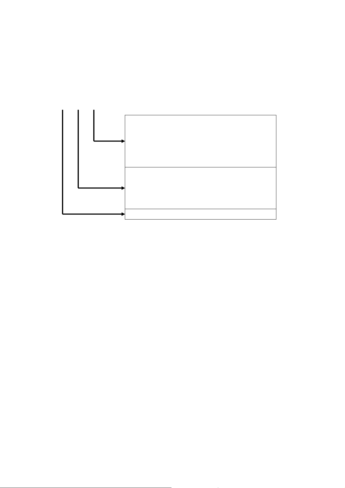
2 Pinout and Terminal Description
WT11i
GND
1
VDD_PA
2
PIO2
3
PIO3
4
UART_ RTS#
5
UART_ RX
6
PCM_OUT
7
USB+
8
USB-
9
UART_ CTS#
10
PCM_IN
11
PCM_CLK
12
PCM_SYNC
13
GND
14
GND
AIO
UART_ TX
PIO5
SPI_MOSI
SPI_MISO
SPI_CLK
SPI_CS#
PIO4
PIO7
PIO6
RESET
VDD
GND
28
27
26
25
24
23
22
21
20
19
18
17
16
15
Figure 1: WT11i connection diagram
PIN
NUMBER
PAD TYPE DESCRIPTION
Input, internal 220kohm
RESET 17
GND
VDD_P
1, 14, 15,
28
2 Supply voltage Supply voltage for the RF power amplifier
pull-down, internal start
reset circuitr
u
GND GND
VDD 16 Supply voltage
Table 1: Supply and RF Terminal Descriptions
Active high reset. Keep high for >5 ms
to cause a reset
Supply voltage for BC4 and the flash
memory
Bluegiga Technologies Oy
Page 8 of 40

put/
p
p
p
p
p
p
PIO PORT
PIO[2] 3
PIO[3] 4
PIO[4] 20
PIO[5] 25
PIO[6] 18
PIO[7] 19
AIO[1] 27 Bi-directional
SPI
INTERFACE
PCM_OUT 7
PIN
NUMBER
PIN
NUMBER
PAD TYPE DESCRIPTION
Bi-directional, programmamble
stre n gth inte rnal pull - down/pull-up
Bi-directional, programmamble
stre n gth inte rnal pull - down/pull-up
Bi-directional, programmamble
stre n gth inte rnal pull - down/pull-up
Bi-directional, programmamble
stre n gth inte rnal pull - down/pull-up
Bi-directional, programmamble
stre n gth inte rnal pull - down/pull-up
Bi-directional, programmamble
stre n gth inte rnal pull - down/pull-up
Table 2: GPIO Terminal Descriptions
PAD TYPE DESCRIPTION
CMOS output, tri-state,
weak internal pull-down
Programmamble input/output
line
Programmamble input/output
line
Programmamble input/output
line
Programmamble input/output
line
Programmamble input/output
line
Programmamble input/output
line
Programmamble analog
in
output line
Synchronous data output
PCM_IN 11
PCM_SYNC 13
PCM_CLK 12
UART
Interfaces
UART_TX 26
UART_RTS# 5
UART_RX 6
UART_CTS# 10
PIN
NUMBER
CMOS input, weak
internal pull-down
Bi-directional, weak
internal pull-down
Bi-directional, weak
internal pull-down
Table 3: PCM Terminal Descriptions
PAD TYPE DESCRIPTION
CMOS output, tri-
state, with weak
internal
CMOS output, tri-
state, with weak
internal
CMOS in p ut, tr istate, with weak
internal
CMOS in p ut, tr istate, with weak
internal
Table 4: UART Terminal Descriptions
ull-u
ull-u
ull-down
ull-down
Synchronous data input
Synchronous data sync
Synchronous data clock
UART data output, active high
UART request to send, active low
UART data input, active high
UART clear to send, active low
Bluegiga Technologies Oy
Page 9 of 40

p
USB Interfaces
USB+ 8 Bidirectional
USB- 9 Bidirectional USB data minus
PIN
NUMBER
PAD TYPE DESCRIPTION
USB data plus with selectable internal 1.5k
ull-up resistor
Table 5: USB Terminal Descriptions
SPI
INTERFACE
SPI_MOSI 24
SPI_CS# 21
SPI_CLK 22
PIN
NUMBER
PAD TYPE DESCRIPTION
CMOS input with weak
-
CMOS input with weak
intern al pull-up
CMOS input with weak
internal pull-do wn
SPI data input
Chip select for Serial Peripheral
Interface, active low
SPI clock
CMOS output, tristate,
SPI_MISO 23
with weak internal pull
SPI data output
down
Table 6: Terminal Descriptions
Bluegiga Technologies Oy
Page 10 of 40

3 Electrical Characteristics
3.1 Absolute Maximum Ratings
Rating
Storage Temperature
VDD_PA, VDD
Other Term inal Voltages
Table 7: Absolute Maximum Ratings
Min Max Unit
-40 85 °C
-0.4 3.6 V
VSS-0.4 VDD+0.4 V
3.2 Recommended Operating Conditions
Rating
Operating Temperature Range
VDD_PA, VDD
*)
*) VDD_PA has an effect on the RF output power.
Table 8: Recommended Operating Conditions
Min Max Unit
-40 85 °C
3.0 3.6 V
3.3 Current Consumption
Packettype Powerlevel MAX AVG Unit
DH1
DH5TX
2DH5 12 dm 106 93
3DH5 12 dm 106 93
RX - - - 39
Sleep - - - 50 µ
Inquiry - 17 dBm 59 mA
Table 9: WT11i Current Consumption
17 dBm 170 72
12 dm 170 54
17 dBm 170 128
12 dm 170 84
mA
A
Bluegiga Technologies Oy
Page 11 of 40
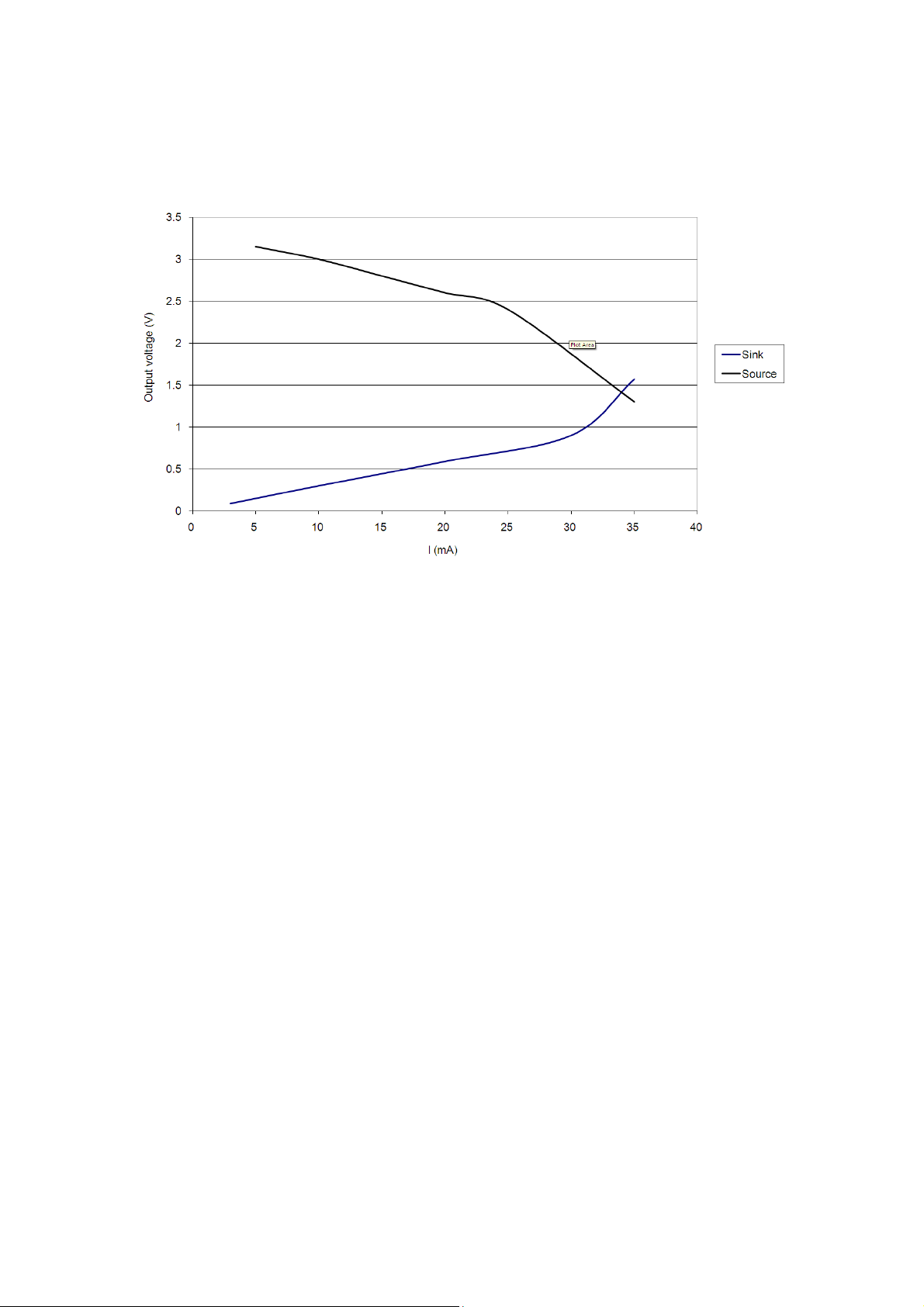
3.4 PIO Current Sink and Source Capability
Figure 2: WT11i PIO Current Drive Capability
3.5 Antenna Specification
Bluegiga Technologies Oy
Page 12 of 40
 Loading...