

WGM110 Wizard Gecko Wi-Fi® Module
Data Sheet
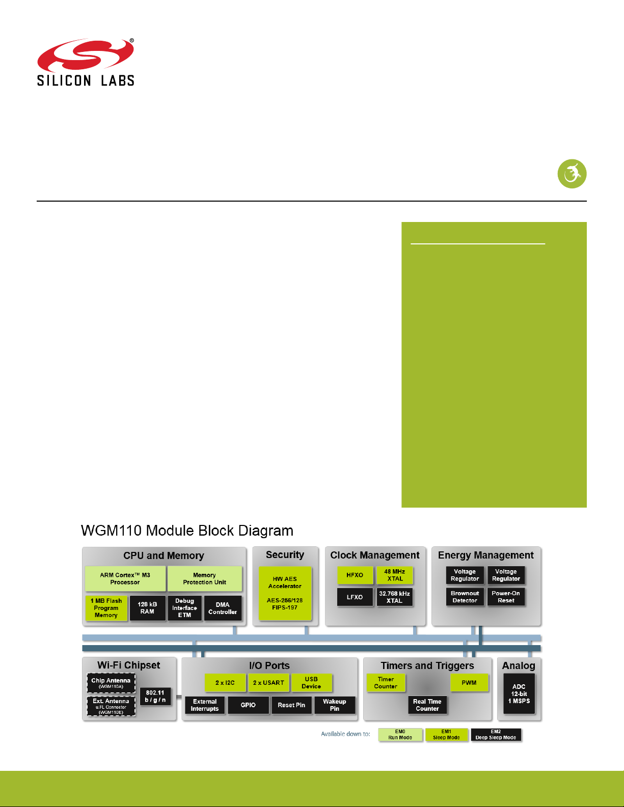
The Wizard Gecko WGM110 is an all-inclusive Wi-Fi® Module targeted for applications
where good RF performance, low-power consumption, and easy application development, together with fast time to market, are key requirements. WGM110 has excellent
RF performance and can provide long range with robust wireless connectivity.
The WGM110 Module integrates all of the necessary elements required for an IoT Wi-Fi
application, including an 802.11b/g/n radio, integrated chip antenna (WGM110A) or an
u.FL connector for an external antenna (WGM110E), certifications, a microcontroller,
Wi-Fi and IP stacks, an HTTP server, and multiple protocols, such as TCP and UDP.
WGM110 can act as a Wi-Fi client or be used as a Wi-Fi access point, making the provisioning of the device as easy as surfing on the web. WGM110 can host BGScript™ end
user applications, which means applications can be designed without relying on an external microcontroller. Alternatively, the Wi-Fi Module can run in Network Co-Processor
(NCP) mode, leaving the complexity of TCP/IP networking to the Module so that the customer’s own host controller can be fully dedicated to processing the customer application tasks. The WGM110 Module also has highly flexible hardware interfaces which allows connection to different peripherals and sensors.
In addition to the Wi-Fi Module itself, Silicon Labs offers support to guide and help developers in using WGM110 to build IoT applications, enabling a quick time to market.
KEY POINTS
• Module variants
• WGM110A (chip antenna)
• WGM110E (u.FL connector)
• 802.11b/g/n compliant
• TX power: +16 dBm
• RX sensitivity: -98 dBm
• Range: up to 450 m
•
CPU core: 32-bit ARM® Cortex-M3
• Flash memory: 1 MB
• RAM: 128 kB
• Modular certification
• FCC
• IC
• Japan
• Korea
• CE compliant
• End-to-end security
• Can host applications
• Small size: 21.0 x 14.4 x 2.0 mm
silabs.com | Smart. Connected. Energy-friendly. Rev. 1.2

1. Key Features
The key features of the WGM110 Module are listed below.
WGM110 Wizard Gecko Wi-Fi® Module Data Sheet
Key Features
Radio Features
• Antenna
• Chip Antenna: WGM110A
• External Antenna: WGM110E (u.FL connector)
• TX Power: +16 dBm
• RX Sensitivity: -98 dBm
• Range: up to 450 m
Wi-Fi Features
• 802.11: b/g/n
• Bit rate: up to 72.2 Mbps
• 802.11 Security: WPA2/WPA Personal, WPA2/WPA Enterprise
and WEP
• STA (Station Mode)
• SoftAP (Soft Access Point Mode): up to 5 clients
• WPS: 1.0 (push-button)
IP Stack
• IP version: IPv4
• IP multicast
• TCP: client/server
• UDP: client/server
• TCP sockets: 20+
• DHCP: client/server
• ARP
• DNS: client/server
• mDNS
• DNS-SD
• HTTP: server
• TLS/SSL: client
Hardware Interfaces
• Host interface: UART/SPI/USB
• Peripheral interfaces
• 2 x USART (UART/SPI)
• 1 x USB (2.0 Full speed)
•
2 x I2C peripheral interfaces
• Up to 32 x GPIO with interrupts
• 8-channel 12-bit ADC
• 2 x TIMER (3 PWM's each)
• Real-time counter
Electrical Characteristics
• Supply voltage: 2.7 V to 4.8 V for the radio block
• Supply voltage: 1.98 V to 3.8 V for the processor block
Power consumption
• 261 mA TX current at +16 dBm
• 81 mA RX current
• 2.4 mA associated idle consumption
• 18.8 μA deep sleep current
Environmental specifications
• Temperature range: -40°C to +85°C
Modular certification
• FCC
• IC
• Japan
• South-Korea
CE Compliant
Software APIs
•
BGAPI™ serial protocol API over UART/SPI/USB for modem
usage
•
BGLIB™ host API which implements BGAPI serial protocol
•
BGScript™ scripting language for standalone usage
Software Development Tools
• Free SDK
MCU Features
•
ARM® Cortex-M3
• 48 MHz
• 128 kB RAM
• 1 MB Flash
Dimensions
• W x L x H: 21.0 mm x 14.4 mm x 2.0 mm
silabs.com | Smart. Connected. Energy-friendly. Rev. 1.2 | 1
WGM110 Wizard Gecko Wi-Fi® Module Data Sheet
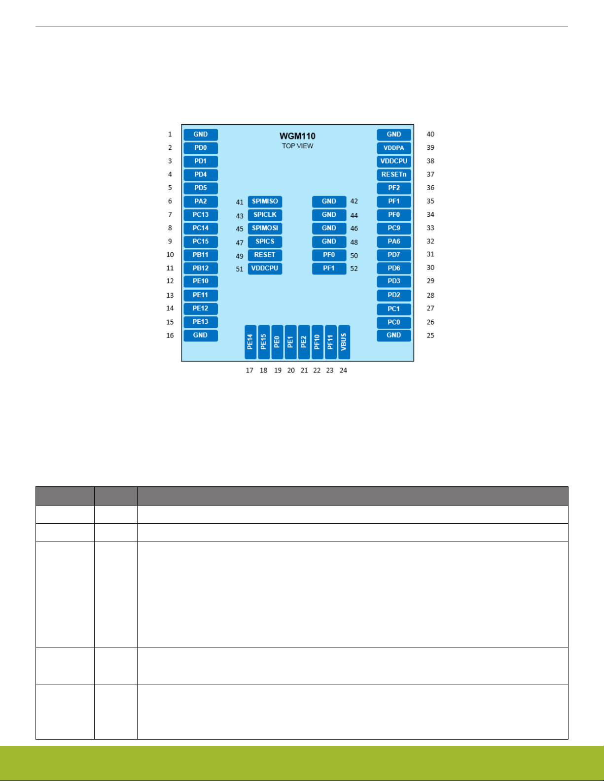
Pinout
2. Pinout
This section describes the pinout of the WGM110 Module.
Pads in the middle of the Module are intended for ground connections and for RF test and production programming, while pads on the
Module edges consist of general purpose input/output, power supply voltage input, ground, and reset signal connections.
Figure 2.1. WGM110 Pinout (Top View)
2.1 Power, Ground and Reset Pads
The table below lists the power, ground, and reset pads of the WGM110 Module.
Table 2.1. WGM110 Power, Ground, and Reset Pads
Pad number Function Description
38, 51 VDDCPU Processor core and peripheral interface power supply.
39 VDDPA RF power amplifier and Wi-Fi core power supply
1, 16, 25, 40,
42, 44, 46,
48
24 VBUS USB VBUS detect input is used to detect the presence of an external USB port bus voltage.
GND Ground.
All ground pads are connected together internally.
Connect ground pads directly to a solid ground plane with maximum number of vias in close proximity to
pads especially at the antenna end.
These ground pads also act as thermal paths which should be used to conduct heat from the module to the
PCB.
Do not use thermal reliefs on ground pads.
When USB is not used connect VBUS to VDDCPU.
37 RESETn Reset signal input. To reset the Module pull this line low.
The reset signals resets both the MCU and the Wi-Fi radio.
Connected to an internal pull-up, can be left floating if not needed.
silabs.com | Smart. Connected. Energy-friendly. Rev. 1.2 | 2

WGM110 Wizard Gecko Wi-Fi® Module Data Sheet
Pinout
2.2 Peripherals and GPIOs
The WGM110 has 32 GPIO pads which can be configured to various peripheral functions, like UART, I2C, USB, etc., or alternatively
they can be used as general purpose I/O pads.
These peripheral functions can be typically configured to multiple pad locations on the devices. Available peripherals, locations, and
I/Os are described in the following sub-sections.
2.2.1 Peripheral and GPIO pads
The table below maps out all supported peripheral functions and the GPIOs (pads) they can be routed to.
Table 2.2. Available Peripheral Functions and GPIO Pad Mapping
PERIPHERAL AND GPIO PAD MAPPING
Port Name PA PB PC PD PE PF
Port Pin #
Pad #
Pad #
2
6
11
12
6
3210112627
0
1
9
131415
7
33
0
1
2
3
4
5
6
7
0
1
2
1011121314
8
9
2
3
28
29
4
5
303119202112131415171834353622
15
0
50
DEBUG
SWCLK •
SWDIO •
I2C0
SCL • • • •
SDA • • • •
I2C1
SCL • •
SDA • •
USART0
UART SPI
CTS CLK • • •
RTS CS • •
1
52
2
10
11
23
RX MISO • • •
TX MOSI • • •
USART1
UART SPI
CTS CLK • •
RTS CS • •
RX MISO • • •
TX MOSI • • •
TIMER0
CC0 • •
CC1 • • •
CC2 • • •
silabs.com | Smart. Connected. Energy-friendly. Rev. 1.2 | 3

®
WGM110 Wizard Gecko Wi-Fi
Module Data Sheet
PERIPHERAL AND GPIO PAD MAPPING
Port Name PA PB PC PD PE PF
Pinout
Port Pin #
Pad #
2
6
11
12
6
3210112627
0
1
9
131415
7
33
0
1
2
3
4
5
6
7
0
1
2
1011121314
8
9
2
3
28
29
4
5
303119202112131415171834353622
Pad #
TIMER1
CCO • • •
CC1 • • •
CC2 • • • •
ADC
CH0 •
CH1 •
CH2 •
CH3 •
CH4 •
CH5 •
CH6 •
CH7 •
15
0
50
1
52
2
10
11
23
USB
DM •
DP •
2.2.2 Peripheral Locations
Many of the peripheral functions can be configured into multiple locations on the GPIO pads. This allows a more flexible configuration of
the Wi-Fi Modules GPIOs.
The following table shows the available locations and the corresponding GPIO pads.
Note: Peripheral function signals must always be grouped to a single location, combining signals from several locations to form a peripheral function is not allowed.
The configuration of the peripheral locations is defined in the hardware configuration file. See UG161: WGM110 Wi-Fi Module Configu-
ration User's Guide for more details.
silabs.com | Smart. Connected. Energy-friendly. Rev. 1.2 | 4

Table 2.3. GPIO Peripheral Locations
WGM110 Wizard Gecko Wi-Fi
®
Module Data Sheet
Pinout
Peripheral Signal
LOC 0 LOC 1 LOC 2 LOC 3 LOC 4 LOC 5 LOC 6 NOTE
name
USART0 SPI MOSI PE10 PE13 PC0
MISO PE11 PE12 PC1
CLK PE12 PC9 PC15
CS PE13 PC14
UART TX PE10 PE13 PC0 1
RX PE11 PE12 PC1 1
CTS PE12 PC15
RTS PE13 PC14
USART1 SPI MOSI PC0 PD0 PD7
MISO PC1 PD1 PD6
CLK PD2 PF0
CS PD3 PF1
UART TX PC0 PD0 PD7 2
RX PC1 PD1 PD6 2
CTS PD2 PF0
RTS PD3 PF1
I2C0 SCL PD7 PC1 PF1 PE13
SDA PD6 PC0 PF0 PE12
I2C1 SCL PB12 PE1
SDA PB11 PE0
USB DM PF10
DP PF11
TIMER0 CC0 PD1 PF0
CC1 PD2 PC0 PF1
CC2 PA2 PA2 PD3 PC1 PF2
TIMER1 CC0 PC13 PE10 PD6
CC1 PC14 PE11 PD7
CC2 PC15 PE12 PB11 PC13
DEBUG SWCLK PF0 PF0 PF0 PF0
SWDIO PF1 PF1 PF1 PF1
Note: The following notes apply to UART Locations:
• 1: USART0 as UART: LOC 5 can be used as an UART without handshake.
• 2: USART1 as UART: LOC 0 can be used as an UART without handshake.
silabs.com | Smart. Connected. Energy-friendly. Rev. 1.2 | 5
WGM110 Wizard Gecko Wi-Fi® Module Data Sheet
Pinout
2.2.3 GPIO Port Pins
The table below lists available Ports and corresponding Port pins in the WGM110 Module and the pads they can be routed to.
Table 2.4. Available GPIO Ports and Pins and Related Pads on the WGM110 Module
Pin → 15 14 13 12 11 10 9 8 7 6 5 4 3 2 1 0
Port ↓
Port A PA6 PA2
Port B PB12 PB11
Port C PC15 PC14 PC13 PC9 PC1 PC0
Port D PD7 PD6 PD5 PD4 PD3 PD2 PD1 PD0
Port E PE15 PE14 PE13 PE12 PE11 PE10 PE2 PE1 PE0
Port F PF11 PF10 PF2 PF1 PF0
2.2.4 GPIO Input and Output Modes
The GPIO pins on the WGM110 Module can be configured as inputs (options are normal input with pull-up or pull-down or with pull-up
with filter or pull-down with filter), outputs (maximum output current 6 mA) or disabled (tristate). The default state of the GPIO pins after
reset is "disabled".
For more information on how to configure the GPIO pins and modes, see WGM110 API Reference Manual.
2.2.5 Interrupt Pins
All GPIO pins may be used as interrupts. WGM110 supports up to 14 asynchronous external pin interrupts with the following limitations:
• All pins with the same number are grouped together and multiplexed to trigger one interrupt.
• Pin 0 from any port cannot be used as an interrupt, because it is reserved for the Module’s internal operation.
• Pin 8 of Port A - F is not available for external use.
Example:
• If PB11 is used as an interrupt pin, then the use of Pin 11 of any other available port as an interrupt is not allowed (PE11 and PF11
cannot be used as an interrupt).
2.3 Debug and RF Test Pads
The table below indicates the pads available for debug and RF test connections.
Table 2.5. Debug and RF Test Pads
Debug and RF Test pads
Port Name RFPORT PF
Pad # 41 43 45 47 34 35
Pad # 50 52
Pad Name SPIMISO SPICLK SPIMOSI SPICS PF0 PF1
DEBUG
SWCLK •
SWDIO •
RF TEST
SPIMISO •
silabs.com | Smart. Connected. Energy-friendly. Rev. 1.2 | 6

WGM110 Wizard Gecko Wi-Fi® Module Data Sheet
Debug and RF Test pads
Port Name RFPORT PF
Pad # 41 43 45 47 34 35
Pad # 50 52
Pad Name SPIMISO SPICLK SPIMOSI SPICS PF0 PF1
SPIMOSI •
SPICLK •
SPICS •
Pinout
silabs.com | Smart. Connected. Energy-friendly. Rev. 1.2 | 7

WGM110 Wizard Gecko Wi-Fi® Module Data Sheet
Interfaces
3. Interfaces
This section describes the features and functionalities of the available host, peripheral, debug, and RF test interfaces.
3.1 Host Interfaces
There are three available host interfaces one of which can be used to connect an external host, typically an MCU, to the WGM110 WiFi Module and use it as a Wi-Fi modem.
3.1.1 UART
UART is one of the available host interfaces on the WGM110 Module, and it is also the default host interface for the WGM110 Modules
delivered from the factory.
The table below shows the features of the UART host interface:
Table 3.1. UART Host Interface Features and Default Values
Parameter Features / Supported ranges Default value
UART baud rate 9600 bps - 6 Mbps 115200 Kbps
Flow control RTS/CTS Enabled
Data bits 8 or 9 8
Parity none, odd, even None
Stop bits 1 or 2 1
Supported USARTs USART0 or USART1 -
Location USART0
• LOC 0
• LOC 3
USART1
• LOC 1
• LOC 2
Host protocol BGAPI serial protocol BGAPI serial protocol
USART 0
LOC 0
silabs.com | Smart. Connected. Energy-friendly. Rev. 1.2 | 8
WGM110 Wizard Gecko Wi-Fi® Module Data Sheet
Interfaces
Figure 3.1. Recommended Schematics: Connecting WGM110 with an External Host Using the UART Interface (USART0 Loc 0)
Note: In the figure above the UART interface is wired using USART0 Location 0 pins.
Note: If handshaking is required, then connect external host CTS to PE13 and external host RTS to PE12.
Note: A programming connector, as shown in the schematics, must be available in the design to enable WGM110 firmware update.
3.1.2 SPI
SPI is one of the available host interfaces on the WGM110 Module. SPI must be always enabled and configured by the user, because it
is not enabled or configured as default.
The table below shows the features of the SPI host interface:
Table 3.2. SPI Host Interface Features
Parameter Features (value ranges)
SPI mode SPI slave
Bit rates 9600 bps - 6 Mbps
Bit order MSB first
Clock polarity and phase Configurable
Supported USARTs USART0 and USART1
Supported locations All locations
Host protocol BGAPI serial protocol
silabs.com | Smart. Connected. Energy-friendly. Rev. 1.2 | 9
WGM110 Wizard Gecko Wi-Fi® Module Data Sheet
Interfaces
The following figure shows the recommended schematics for connecting WGM110 with an external host over SPI. In addition to the
selected USART/SPI port signals, one additional GPIO pin must be dedicated to be used as a notify signal to inform the SPI Master that
data from module is available.
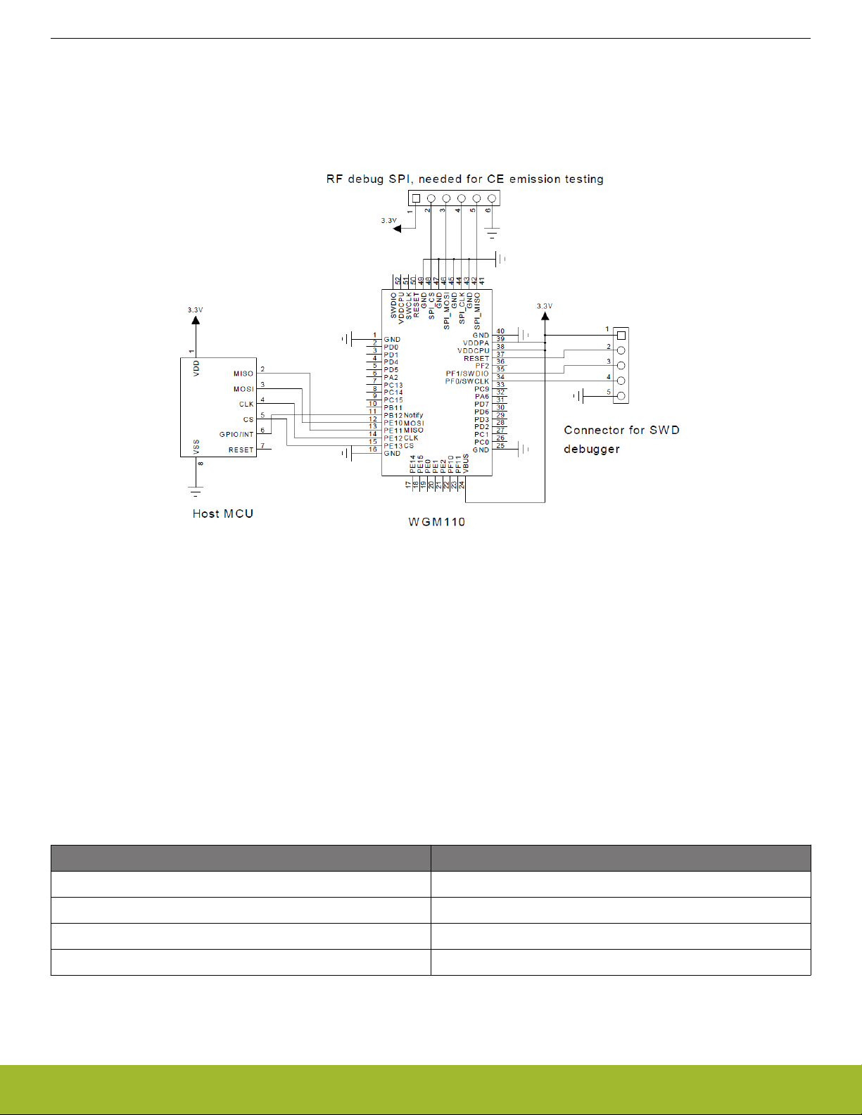
Note: The SPI host interface can only be used as a SPI Slave.
Figure 3.2. Connecting WGM110 with an External Host Using the SPI Interface
Note: In the figure above, the SPI interface is wired using USART0 Location 0 pins.
Note: Pin PB12 is configured as an output and used to notify the external host (SPI Master) that the WGM110 Module has data to send
to the host.
3.1.3 USB
USB is one of the available host interfaces on the WGM110 Module. USB must be always enabled and configured by the user, because
it is not enabled or configured as default.
The table below shows the features of the USB host interface:
Table 3.3. USB Host Interface Features
Parameter Compatibility
USB mode USB device
USB version 2.0 Full speed
USB device class CDC/ACM (COM port)
Host protocol BGAPI serial protocol
silabs.com | Smart. Connected. Energy-friendly. Rev. 1.2 | 10
WGM110 Wizard Gecko Wi-Fi® Module Data Sheet
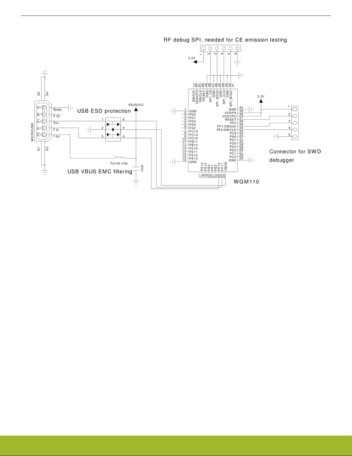
The next figure shows the recommended schematics for connecting WGM110 Module with an external host over USB.
Interfaces
Figure 3.3. Connecting the WGM110 Module with an External Host using the USB Interface
Note: When using the USB interface, the VBUS signal should be connected to the USB host's VBUS line.
Note: If the VBUS line is not available on the host, the module's VBUS signal should be connected to the VDDCPU.
Note: If the USB is not used at all, the VBUS signal should be connected to the VDDCPU.
3.2 Peripheral Interfaces and Functions
There are several different types of peripheral interface connections available on the WGM110 Module. External sensors and peripheral
chips can be connected using the USART (UART/SPI) and I2C interfaces. In addition to the above mentioned connections, WGM110
includes two timers for PWM applications, an 8-channel 12-bit ADC converter and a real time counter.
silabs.com | Smart. Connected. Energy-friendly. Rev. 1.2 | 11

WGM110 Wizard Gecko Wi-Fi
®
Module Data Sheet
Interfaces
3.2.1 USART (UART/SPI)
The Universal Synchronous/Asynchronous Receiver/Transmitter (USART) provides a flexible serial I/O interface. It supports full duplex
asynchronous UART communication up to 6 Mbps. Both SPI Master and Slave modes are also supported up to 6 Mbps.
Software emulated RTS/CTS handshaking is supported. For this reason there may be up to two extra data bytes transmited by the
Module after the host's RTS has been pulled high.
Figure 3.4. USART
3.2.2 I2C
The I2C peripheral provides an interface between the WGM110 Module and a serial I2C bus. It is capable of acting as a I2C Master.
Standard-mode is supported, allowing transmission rates up to 100 Kbps.
Figure 3.5. WGM110 Acting as an I2C Master with Several I2C Slaves Connected to the Module
3.2.3 Timer / PWM
Timer peripherals count events and can be used to generate PWM outputs. The core of each timer is a 16-bit counter. There are two
timers, each with three separate outputs configurable for PWM applications.
3.2.4 Analog to Digital Converter (ADC)
The ADC inside the WGM110 Module is based on Successive Approximation Register (SAR) architecture and has a resolution of up to
12 bits (1 MSPS). The ADC includes user selectable integrated voltage references but also allows the use of an external reference.
There are 8 fixed GPIO pins configurable for single-ended ADC inputs.
3.3 Firmware Update and RF Test Interfaces
Firmware updates can be done over the ARM Serial Wire Debug (SWD) interface, which is the recommended firmware update interface
for development and production programming.
It is also possible to update the firmware using the Device Firmware Update (DFU) protocol by using an interface configured as the host
interface (UART, SPI or USB).
silabs.com | Smart. Connected. Energy-friendly. Rev. 1.2 | 12
WGM110 Wizard Gecko Wi-Fi
®
Module Data Sheet
Interfaces
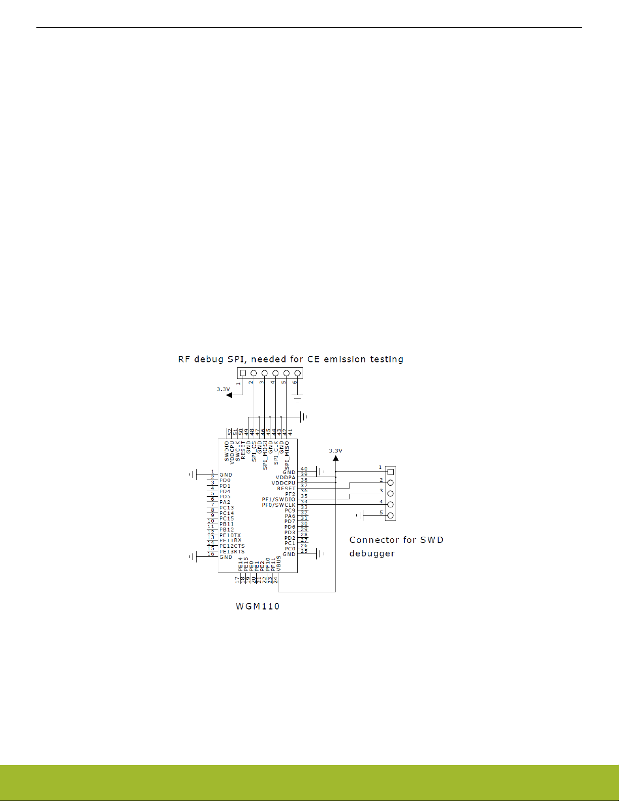
3.3.1 ARM Serial Wire Debug (SWD)
The WGM110 Module contains a 2-wire ARM SWD interface for programming and debugging. It is recommended that the pads of this
interface are exposed in the application design to allow firmware updates and debugging.
3.3.2 Device Firmware Upgrade (DFU)
The firmware can be updated over the configured host interface (UART, SPI, or USB) using the Device Firmware Upgrade (DFU) protocol. This method is intended to be used for field updates of the firmware, for example, when updating the WGM110 Module firmware
from a connected host using the BGAPI serial protocol.
Note: You cannot update the bootloader using the DFU protocol. Bootloader update must be done using the SWD Debug interface.
Note: In case the DFU recovery mode is not useable for any reason, the SWD bus is always available at boot when the RESET pin of
the WGM110 Module is being pulled down.
3.3.3 RF Test Interface
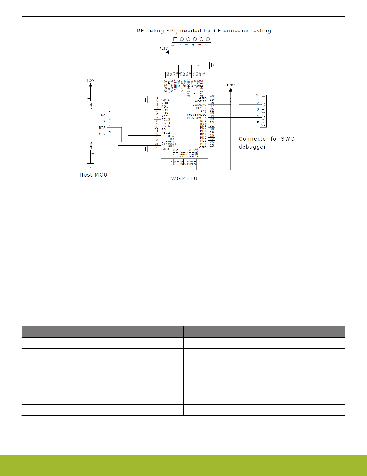
There are dedicated pads on the WGM110 Module that are used to enable the Wi-Fi radio test modes. These test modes would typically be used if RF measurements relating to CE or any other certification requirements are needed. More specifically, RF Test pads are
used to enable the TX and RX test modes of the WGM110 Module.
3.3.4 Reference Schematic for SWD Debug and RF Test Interfaces
The schematic below shows the necessary connections needed for using the SWD and RF test interfaces.
Figure 3.6. SWD Debug and RF Test Interface Connections
3.4 Real Time Counter (RTC)
The Real Time Counter is a 24-bit counter providing timekeeping functions for the WGM110 Module.
silabs.com | Smart. Connected. Energy-friendly. Rev. 1.2 | 13
 Loading...