

WFM200S Data Sheet
The Silicon Labs WFM200S is an Ultra Low Power Wi-Fi® transceiver or network co-processor (NCP) SiP module targeted for applications where optimal RF performance, lowpower consumption, and secure end-to-end solution, together with fast time to market,
are key requirements.
The very compact 6.5mm x 6.5mm WFM200S SiP module contains an embedded antenna, high frequency crystal, and shield. This all-inclusive module offer the fastest time
to market.
The WFM200S integrates a balun, T/R switch, LNA and PA for the best possible RF performance. Co-existence with external 2.4GHz transceivers is supported via a PTA interface.
WFM200S has been optimized for resource and power constrained devices at the RF,
protocol and firmware levels. Power conscious devices can take advantage of these features in both active and idle/sleep modes.
For security sensitive applications, the WFM200S provides secure boot and a secure,
encrypted host interface. Robust security is made possible with the native integrated
True Random Number Generator and OTP memory for confidential encryption key storage.
The WFM200S fits well witl Linux-based and RTOS-based host processors. WFM200S
supports both the 802.11 split MAC architecture and the 802.11 full MAC software architecture. WFM200S communicates with the external host controller over the SPI or SDIO
interface.
KEY POINTS
• IEEE 802.11 b/g/n compliant
• Embedded high efficiency antenna
• Integrated crystal and shield
• 105°C ambient temp support
• TX power: up to +15.1 dBm
• RX sensitivity: -96.3 dBm
• Integrated switched antenna diversity
support
• Ultra low power consumption
• Secure and signed software
• Encrypted host interface communication
• Linux and RTOS host support
• Certifications
• CE, FCC, ISED, Japan
• 6.5 x 6.5 mm SiP Module
silabs.com | Building a more connected world. Preliminary Rev. 0.51
This information applies to a product under development. Its characteristics and specifications are subject to change without notice.

Table of Contents
1. Features List ...............................4
2. Ordering Information ............................5
3. System Overview ..............................6
3.1 Introduction ...............................6
3.2 Wi-Fi Supported 2.4 GHz Bandwidth and Channels .................7
4. Electrical Specifications ...........................8
4.1 Absolute Maximum Ratings..........................8
4.2 Operating Conditions ............................9
4.3 Power Consumption ............................10
4.4 RF Transmitter General Characteristics .....................11
4.4.1 RF Transmitter Characteristics .......................12
4.5 RF Receiver General Characteristics ......................12
4.5.1 RF Receiver Characteristics ........................13
4.6 Reference Oscillator and Low Power Clock Characteristics ...............14
4.6.1 Low Power 32.768 kHz Clock Input Requirements ................14
4.7 Interface Terminal Characteristics .......................14
4.7.1 Supply Terminal Specifications .......................14
4.7.2 Digital I/O Terminal Specifications ......................15
4.8 Host Interface ..............................15
4.8.1 SPI Specification ............................17
4.8.2 SDIO Specification ...........................18
5. Typical Applications and Connections .....................19
5.1 Typical Application Circuit for SDIO Host Interface ..................19
5.2 Typical Application Circuit for SPI Host Interface ..................20
5.3 Power States and Low-Power Modes .....................21
5.4 RF Connections .............................21
5.4.1 RF Ports ..............................21
5.4.2 Antenna Diversity ...........................21
5.4.3 Embedded Antenna Pins .........................21
5.5 Clocks .................................21
5.5.1 High Frequency Crystal Oscillator ......................21
5.5.2 LP_CLK Port .............................22
5.6 Multi-Protocol Coexistence ..........................22
6. Pin Descriptions .............................23
7. Package Outline .............................25
8. Land Pattern ..............................29
9. Top Marking............................... 31
silabs.com
| Building a more connected world. Preliminary Rev. 0.51 | 2

10. Tape and Reel Specifications ........................32
10.1 Tape and Reel Packaging..........................32
10.2 Reel and Tape Specifications ........................32
10.3 Orientation and Tape Feed .........................34
10.4 Tape and Reel Box Dimensions ........................34
10.5 Moisture Sensitivity Level ..........................34
11. Software Reference ...........................35
11.1 Host and Device Software..........................35
11.1.1 Split MAC ..............................35
11.1.2 Full MAC ..............................36
11.1.3 Software Documentation .........................36
11.2 Security ................................36
11.2.1 Secure Device ............................36
11.2.2 Secure Boot .............................37
11.2.3 Secure Link (WFM200SS only) ......................37
11.3 Startup, Sleep and Shutdown ........................37
11.3.1 Power On, Reset, and Boot ........................37
11.3.2 Sleep and Snooze Modes ........................37
11.3.3 Shutdown Mode............................38
12. Certifications ..............................39
12.1 Qualified External Antenna Types .......................39
12.2 CE .................................39
12.3 FCC .................................40
12.4 ISED Canada ..............................41
12.5 Japan ................................43
12.6 Locating the Module Close to Human Body ....................44
13. Revision History............................. 45
silabs.com
| Building a more connected world. Preliminary Rev. 0.51 | 3

1. Features List
The WFM200S Wi-Fi SiP module key features are listed below.
Applications
• Industrial, Home and Buidling automation
• Home appliances
• Security solutions
• Retail and Commercial
• Commercial transportation
• Consumer medical
• Sports and Fitness
Features
• 802.11 b/g/n Wi-Fi NCP including the radio, baseband, MAC,
security and host interface
• Integrated LNA, PA and Balun
• Integrated 38.4 MHz Crystal and embedded antenna
• OTP included removing the need for an external EEPROM
• Ultra low power optimized solution
• End-to-end security with hardware protected secure boot and
encrypted host interface (optional)
• 802.11 split and full MAC architecture support
• Complete Network Co-Processor (NCP) support for Linux and
RTOS external hosts
Standards/IEEE 802.11 and WFA
• b - symbol rates: up to 11 Mbps
• g - symbol rates: up to 54 Mbps
• n - symbol rates: up to 72.2Mbps
• d - regulatory domains
• e - QoS as per definition in WMM specification
• i - as per definition in WPA2 specification
• w - protected management frames
• WMM Power save
• WPA/WPA2 Personal
• Supported with Linux UMAC:
• WPA2 Enterprise
• WPS - Wi-Fi Protected Setup
Key MAC and Baseband Features
• 1x1 802.11n (20 MHz) with full 802.11 b/g compatibility,
72.2Mbps
• Greenfield Tx/Rx for 802.11n optimal performance
• Short Guard Interval (SGI) for 802.11n optimal throughput
• A-MPDU Rx and Tx for high MAC throughput
• Block acknowledgement for several frames
• Rx Defragmentation
• Roaming supported
• Client, SoftAP modes supported
• Concurrent AP + STA supported on different channels
WFM200S Data Sheet
Features List
RF Features
• Tx Power: +15.1 dBm
• Rx Sensitivity: -96.3 dBm
• 2 x 2.4GHz antenna pads for switched antenna diversity support
• 2.4GHz co-existence; 2-, 3- and 4-wire PTA support
• Integrated Balun, T/R switch, LNA and PA for 2.4GHz
Power Consumption
• Rx (@DSSS-1Mbps): 42.3 mA
• Tx (15.1 dBm @DSSS-1Mbps): 145 mA
• Associated DTIM3 average current : 298 μA
• Associated Sleep Current : 22 μA
• Shutdown mode: 0.5 μA
Security and Encryption Features
• Secure boot with roll-back prevention
• Encrypted host interface, dedicated hardware acceleration
block (optional)
• Integrated True Random Number Generator
• Secure key storage using protected OTP technology
• AES/WEP hardware acceleration
Host Interfaces
• SDIO (1-bit and 4-bit SD mode @ 26MHz)
• SPI (1-bit @ 52MHz)
Peripheral Interfaces
• External 32kHz crystal for low power
• GPIOs (including wake-up and Tx/Rx activity monitoring)
ROHS/REACH Compliant
Certifications
• CE, FCC, ISED, Telec
Electrical Characteristics
• 1.62V - 3.6V (VDDD, VDDIO)
• 3.0 - 3.6V (VDDPA)
Packaging
• 6.5x6.5 LGA58 SiP Module
• Temperature range: -40°C to +105°C
silabs.com | Building a more connected world. Preliminary Rev. 0.51 | 4

WFM200S Data Sheet
Ordering Information
2. Ordering Information
This section contains ordering information for WFM200S.
Note: The parts may be referred to by the product family friendly name (WFM200S), or by the model names (WFM200SA,
WFM200SN), or by the full orderable part numbers throughout this document
Table 2.1. WFM200S Ordering Information (R indicates Full Reel)
Part Number Description Antenna
Type
WFM200S022XNA2(R) WFM200S 802.11bgn NCP Embedded 6.5x6.5 LGA52 SiP module
WFM200SS22XNA2(R) WFM200S 802.11bgn NCP
Secure host interface
WFM200S022XNN2(R) WFM200S 802.11bgn NCP External only 6.5x6.5 LGA52 SiP module
WFM200SS22XNN2(R) WFM200S 802.11bgn NCP
Secure host interface
Embedded 6.5x6.5 LGA52 SiP module
External only 6.5x6.5 LGA52 SiP module
Package
silabs.com | Building a more connected world. Preliminary Rev. 0.51 | 5
WFM200S Data Sheet
System Overview
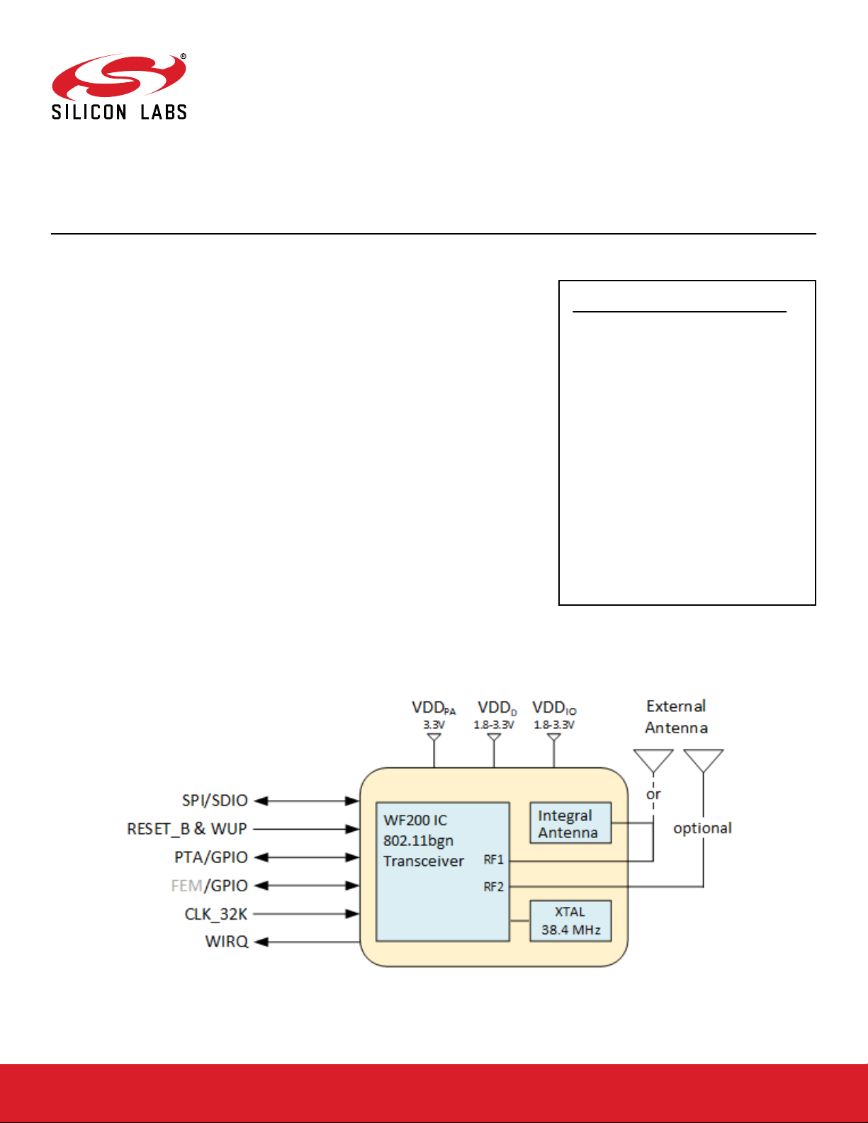
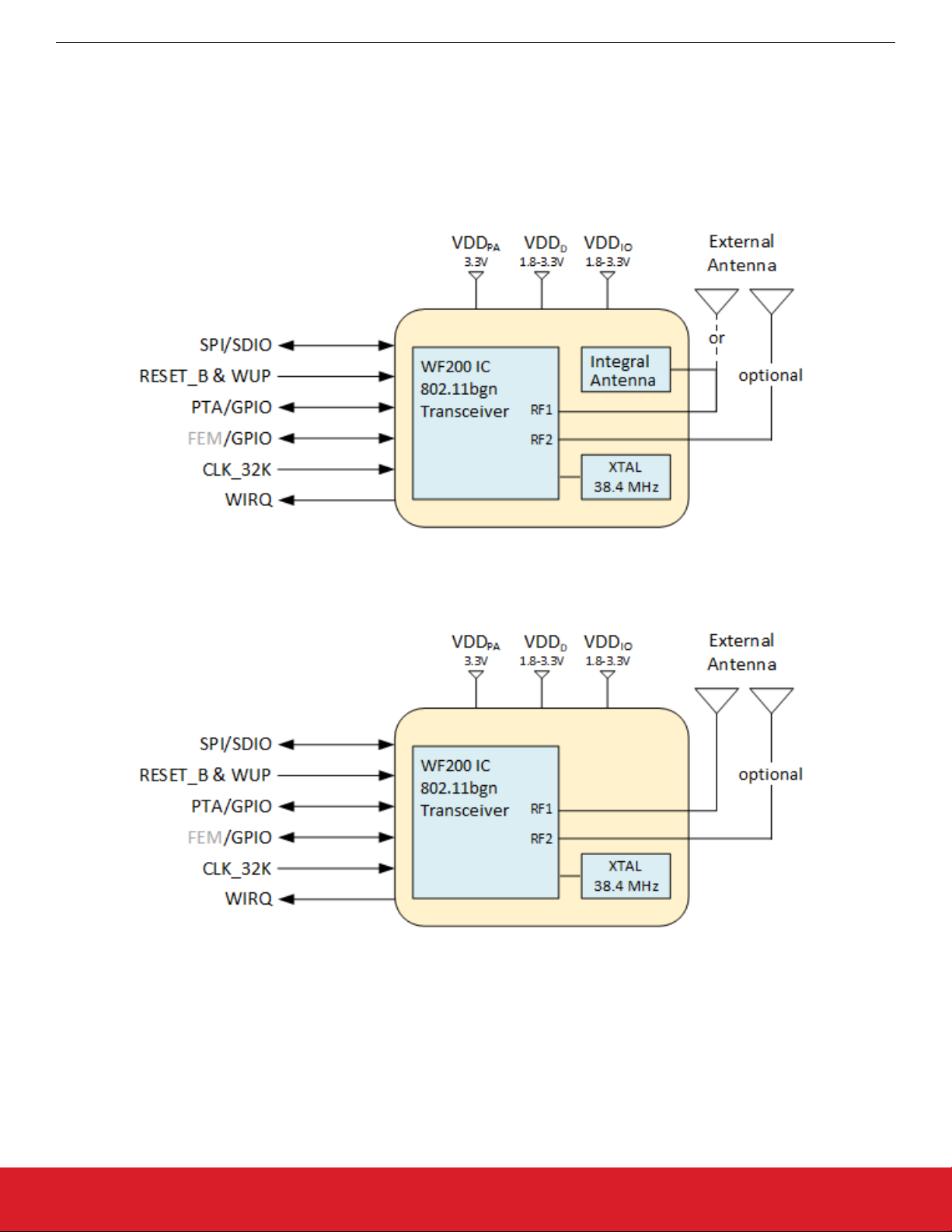
3. System Overview
3.1 Introduction
WFM200S is a WiFi network co-processor module optimized for RF performance, low energy, and low cost, with two antenna ports,
Crystal Oscillator, One Time Programmable Memory, and several GPIOs for interfacing with multi-protocol and RF Front End Module
controls.
Figure 3.1. WFM200SA Block Diagram
Figure 3.2. WFM200SN Block Diagram
silabs.com | Building a more connected world. Preliminary Rev. 0.51 | 6

3.2 Wi-Fi Supported 2.4 GHz Bandwidth and Channels
Supported operating frequencies and bandwidth
Table 3.1. Supported Wi-Fi Modulations, BW, and Channels
Parameter Symbol Test Condition Min Typ Max Unit
WFM200S Data Sheet
System Overview
Channel Center Frequency CHAN Subject to Regulatory Agency 2412
2484
MHz
Channel Bandwidth BW — 20 — MHz
Note:
1. Channel 14 only supports 1 and 2 Mbps modulations.
silabs.com | Building a more connected world. Preliminary Rev. 0.51 | 7

WFM200S Data Sheet
Electrical Specifications
4. Electrical Specifications
All electrical parameters in all tables are specified under the following conditions, unless stated otherwise:
• Typical values are based on TA = 25 °C; V
• Radio performance numbers are measured in conducted mode, based on Silicon Labs reference designs
• WFM200S features and benefits depend on system configuration and may require specific driver, firmware or service activation.
Learn more at https://www.silabs.com/products/wireless/wi-fi
Refer to Section 4.2 Operating Conditions for more details about operational supply and temperature limits.
4.1 Absolute Maximum Ratings
Stresses above those listed below may cause permanent damage to the device. This is a stress rating only and functional operation of
the devices at those or any other conditions above those indicated in the operation listings of this specification is not implied. Exposure
to maximum rating conditions for extended periods may affect device reliability. For more information on the available quality and reliability data, see the Quality and Reliability Monitor Report at http://www.silabs.com/support/quality/pages/default.aspx.
Parameter Symbol Test Condition Min Typ Max Unit
, V
VDD_IO
VDD
, V
VDD_PA
= 3.3V
Table 4.1. Absolute Maximum Ratings
Storage temperature T
Junction temperature TJ
RF power level at RF1 and
P
RF2 ports
Supply voltage to VDD_PA,
VDD
VDD_IO, VDD
Voltage on all other pins
VG
(GPIO, Host interface, PTA,
etc.)
Current into any GPIO pin IO
Sum of current into all GPIO
IO
pins
Range of load impedance at
LOAD
RF1 and RF2 pins during TX
STG
MAX
RFMAX
MAX
MAX
MAX
ALL_MAX
TX
-40 — 150 °C
-40 — 125 °C
— — 10 dBm
-0.3 — 3.6 V
-0.3 — VDDIO +
V
0.3 V
— — 20 mA
— — 150 mA
— — 10:1 VSWR
silabs.com | Building a more connected world. Preliminary Rev. 0.51 | 8

WFM200S Data Sheet
Electrical Specifications
4.2 Operating Conditions
Table 4.2. Recommended Operating Conditions
Parameter Symbol Test Condition Min Typ Max Unit
Ambient operating temperature
Junction operating temperature
DC supply voltage to
VDD_PA
1
Nominal supply voltage to
VDD
Nominal supply voltage to
VDD_IO
Note:
1. V
must always be greater than or equal to V
VDD_PA
T
A
T
J
V
VDD_PA
V
VDD
V
VDD_IO
VDD
-40 — 105 °C
-40 — 125 °C
3.0 3.3 3.6 V
1.62 1.8 3.6 V
1.62 1.8 3.6 V
.
silabs.com | Building a more connected world. Preliminary Rev. 0.51 | 9

4.3 Power Consumption
WFM200S Data Sheet
Electrical Specifications
Unless otherwise indicated, V
VDD_PA
= 3.3 V, V
VDD
= V
VDD_IO
= 1.8 V.
Table 4.3. Power Consumption
Parameter Symbol Test Condition Min Typ Max Unit
TX mode current I
TX
802.11.b: 1 Mbps, from VDD_PA
— 99.4 — mA
at 3.3 V
802.11.b: 11 Mbps, from VDD_PA
— 95.6 — mA
at 3.3 V
802.11.g: 6 Mbps, from VDD_PA
— 95.2 — mA
at 3.3 V
802.11.g: 54 Mbps, from VDD_PA
— 92.6 — mA
at 3.3 V
802.11.n: MCS = 0, from VDD_PA
— 94.9 — mA
at 3.3 V
802.11.n: MCS = 7, from VDD_PA
— 92.3 — mA
at 3.3 V
802.11.b: 1 Mbps, from 1.8 V sup-
— 45.5 — mA
plies (VDD, VDD_IO)
802.11.b: 11 Mbps, from 1.8 V
— 45.4 — mA
supplies (VDD, VDD_IO)
RX mode current I
RX
802.11.g: 6 Mbps, from 1.8 V supplies (VDD, VDD_IO)
802.11.g: 54 Mbps, from 1.8 V
supplies (VDD, VDD_IO)
802.11.n: MCS = 0, from 1.8 V
supplies (VDD, VDD_IO)
802.11.n: MCS = 7, from 1.8 V
supplies (VDD, VDD_IO)
802.11.b: 1 Mbps, from 1.8 V supplies (VDD, VDD_IO)
802.11.b: 11 Mbps, from 1.8 V
supplies (VDD, VDD_IO)
802.11.g: 6 Mbps, from 1.8 V supplies (VDD, VDD_IO)
802.11.g: 54 Mbps, from 1.8 V
supplies (VDD, VDD_IO)
802.11.n: MCS = 0, from 1.8 V
supplies (VDD, VDD_IO)
802.11.n: MCS = 7, from 1.8 V
supplies (VDD, VDD_IO)
— 46.7 — mA
— 47.4 — mA
— 46.7 — mA
— 47.4 — mA
— 42.3 — mA
— 43.0 — mA
— 45.4 — mA
— 47.8 — mA
— 45.2 — mA
— 48.3 — mA
Sleep current on power supply pins
silabs.com | Building a more connected world. Preliminary Rev. 0.51 | 10
1
I
SLEEP
VDD_PA pin, V
VDD pin, V
VDD
VDD_IO pin, V
= 3.3 V — 66 — nA
VDD_PA
= 1.8 V — 18.7 — µA
= 3.3 V — 3.5 — µA
VDD_IO

WFM200S Data Sheet
Electrical Specifications
Parameter Symbol Test Condition Min Typ Max Unit
Snooze current on power
supply pins
2
Shutdown current on power
supply pins
3
Average current for DTIM=1
Interval Profile
4
Average current for DTIM=3
Interval Profile
4
Average current for DTIM=10
Interval Profile
4
I
SNOOZE
I
SHUTDOWN
I
LP_DTIM1
I
LP_DTIM3
I
LP_DTIM10
VDD_PA pin, V
VDD pin, V
VDD
VDD_IO pin, V
VDD_PA pin, V
VDD pin, V
VDD
VDD_IO pin, V
VDD_PA pin, V
VDD pin, V
VDD
VDD_IO pin, V
VDD_PA pin, V
VDD pin, V
VDD
VDD_IO pin, V
VDD_PA pin, V
VDD pin, V
VDD
VDD_IO pin, V
= 3.3 V — 66 — nA
VDD_PA
= 1.8 V — 1146 — µA
= 3.3 V — 51 — µA
VDD_IO
= 3.3 V — 67 — nA
VDD_PA
= 1.8 V — 83.8 — nA
= 3.3 V — 49 — nA
VDD_IO
= 3.3 V — 154 — nA
VDD_PA
= 1.8 V — 891 — µA
= 3.3 V — 3.7 — µA
VDD_IO
= 3.3 V — 128 — nA
VDD_PA
= 1.8 V — 294 — µA
= 3.3 V — 3.6 — µA
VDD_IO
= 3.3 V — 118 — nA
VDD_PA
= 1.8 V — 103 — µA
= 3.3 V — 3.7 — µA
VDD_IO
Note:
1. All memory is retained in sleep mode. WUP on timer and/or interrupt.
2. All memory is retained and Xtal oscillator is kept on if no 32 kHz clock is provided.
3. Requires complete start-up sequence to resume operation.
4. All DTIM currents assume a 1 ms beacon time duration with a beacon interval of 102.4ms from the AP.
4.4 RF Transmitter General Characteristics
Unless otherwise indicated, typical conditions are: Operating Ambient Temp = 25 °C, V
VDD_IO
= V
= 1.8 V; V
VDD
VDD_PA
= 3.3V, center
frequency = 2,442 MHz, and measured in 50 Ω test equipment attached at antenna port. The output power levels are backed off to
ensure compliance into a 2:1 VSWR antenna at the worst phase angles. More details are in UG395: WFM200 Hardware Design User's
Guide.
Measurements for this specification are made using the RF_1 port. See Section 5.4.1 RF Ports.
silabs.com | Building a more connected world. Preliminary Rev. 0.51 | 11

WFM200S Data Sheet
Electrical Specifications
4.4.1 RF Transmitter Characteristics
Table 4.4. RF Transmitter Characteristics
Parameter Symbol Test Condition Min Typ Max Unit
RMS output power with compliance for antennas up to
2:1 VSWR
Second Harmonic Level for
POUT_MAX_PA Setting
Carrier Suppression per
802.11-2012 for POUT_MAX
PA setting
POUT
HPPA
HD2
C
SUP
MAX_RMS_
MAX
802.11b: 1 Mbps — 15.1 — dBm
802.11b: 11 Mbps — 13.0 — dBm
802.11g: 6 Mbps — 12.5 — dBm
802.11g: 54 Mbps — 7.1 — dBm
802.11n: MCS=0 — 12.1 — dBm
802.11n: MCS=7 — 5.0 — dBm
802.11b: 1 Mbps — -47.9 — dBm
802.11b: 11 Mbps — -49.1 — dBm
802.11g: 6 Mbps — -50.2 — dBm
802.11g: 54 Mbps — -54.2 — dBm
802.11n: MCS=0 — -50.4 — dBm
802.11n: MCS=7 — -55.6 — dBm
802.11b: 1 Mbps — -45.8 — dBr
802.11b: 11 Mbps — -44.3 — dBr
802.11g: 6 Mbps — -36.9 — dBr
802.11g: 54 Mbps — -35.9 — dBr
802.11n: MCS=0 — -39.6 — dBr
802.11n: MCS=7 — -31.4 — dBr
POUT variation from
VDD_PA=3.0 V to 3.6 V
POUT variation across temperature
POUT
V
POUT
T
MAX_VAR_
MAX_VAR_
VDD_PA = 3.0 V to 3.6 V, Meas-
— 1.6 — dB
ured on single channel
25C to 85C — 0.9 — dB
4.5 RF Receiver General Characteristics
Unless otherwise indicated, typical conditions are: Operating Ambient Temp = 25 °C, V
VDD_IO
frequency = 2,442 MHz, and measured in 50 Ω test equipment attached at antenna port.
Measurements for this specification are made using the RF_1 port. See Section 5.4.1 RF Ports.
= V
= 1.8 V; V
VDD
VDD_PA
= 3.3V, center
silabs.com | Building a more connected world. Preliminary Rev. 0.51 | 12

WFM200S Data Sheet
Electrical Specifications
4.5.1 RF Receiver Characteristics
Table 4.5. RF Receiver Characteristics
Parameter Symbol Test Condition Min Typ Max Unit
RX Sensitivity for 8% FER
(1024 Octet)
RX Sensitivity for 10% PER
(1024 Octet)
RX Sensitivity for 10% PER
(4096 Octet)
Adjacent Channel ( ± 30
MHz) Selectivity with desired
signal at 6 dB above reference sensitivity for 8% FER
(1024 Octet)
Adjacent Channel ( ± 25
MHz) Selectivity with desired
signal at 3 dB above reference sensitivity for 10% PER
(1024 Octet)
Adjacent Channel ( ± 25
MHz) Selectivity with desired
signal at 3 dB above reference sensitivity for 10% FER
(4096 Octet)
SENS
SENS
SENSE
ACS
WB
ACS
WG
ACS
WN
B
802.11b: 1 Mbps — -96.3 — dBm
802.11b: 11 Mbps — -88.0 — dBm
G
802.11g: 6 Mbps — -91.5 — dBm
802.11g: 54 Mbps — -74.6 — dBm
N
802.11n: MCS=0 — -91.0 — dBm
802.11n: MCS=7 — -71.7 — dBm
802.11b: 1 Mbps — 56.0 — dBc
802.11b: 11 Mbps — 45.2 — dBc
802.11g: 6 Mbps — 47.9 — dBc
802.11g: 54 Mbps — 32.2 — dBc
802.11n: MCS=0 — 47.5 — dBc
802.11n: MCS=7 — 29.9 — dBc
2nd Adjacent Channel Selecitivity ( ± 50 MHz) with desired at 6 dB above reference sensitivity 8% FER
(1024 Octet)
2nd Adjacent Channel Selecitivity ( ± 50 MHz) with desired at 3 dB above reference sensitivity 10% PER
(1024 Octet)
2nd Adjacent Channel Selecitivity ( ± 50 MHz) with desired at 3 dB above reference sensitivity 10% PER
(4096Octet)
RX Max Strong Signal for
8% FER (1024 Octet)
RX Max Strong Signal for
10% PER (1024 Octet)
RX Max Strong Signal for
10% PER (4096 Octet)
A2CS
A2CS
A2CS
RX
SAT_B
RX
SAT_G
RX
SAT_N
WB
WG
WN
802.11b: 1 Mbps — 57.5 — dBc
802.11b: 11 Mbps — 52.0 — dBc
802.11g: 6 Mbps — 52.4 — dBc
802.11g: 54 Mbps — 36.4 — dBc
802.11n: MCS=0 — 51.7 — dBc
802.11n: MCS=7 — 33.4 — dBc
802.11b: 1 Mbps — -4.0 — dBm
802.11b: 11 Mbps — -10.0 — dBm
802.11g: 6 Mbps — -9.0 — dBm
802.11g: 54 Mbps — -9.0 — dBm
802.11n: MCS=0 — -9.0 — dBm
802.11n: MCS=7 — -9.0 — dBm
silabs.com | Building a more connected world. Preliminary Rev. 0.51 | 13

WFM200S Data Sheet
Electrical Specifications
Parameter Symbol Test Condition Min Typ Max Unit
RX Channel Power Indicator
Accuracy worst case with input swetp from -60 dBm to
RX_SAT
RX Channel Power Indicator
Accuracy Worst Case with
input signal swept from reference sensitivity to -69 dbm
RX Channel power Indicator
Step Size
RCPI
RCPI
RCPI
TOLS
TOLW
STEP
802.11b: 1 Mbps — -4.5 — dB
802.11g: 6 Mbps — -2.8 — dB
802.11n: MCS=7 — -3.3 — dB
802.11b: 1 Mbps — -1.3 — dB
802.11g: 6 Mbps — -1.4 — dB
802.11n: MCS=7 — -1.0 — dB
802.11b: 1 Mbps — 0.5 — dB
802.11g: 6 Mbps — 0.5 — dB
802.11n: MCS=7 — 0.5 — dB
4.6 Reference Oscillator and Low Power Clock Characteristics
The WFM200S contains a built-in 38.4 MHz XTAL to generate the reference clock.
To achieve low power operation during power save modes, an external 32.768 KHz clock is required.
4.6.1 Low Power 32.768 kHz Clock Input Requirements
Table 4.6. Low Power 32.768 kHz Clock Input Requirements
Parameter Symbol Test Condition Min Typ Max Unit
Nominal Frequency of
FNOM
LPCLK
— 32.768 — KHz
LP_CLK
Frequency Tolerance of
LP_CLK over all conditions
Load of LP_CLK pin R
Input Level at LP_CLK SIGL
1
FTOL
LPCLK
LPCLK
LPCLK
-1000 — 1000 ppm
— 30 — KOhm
0.7 *
— VDD_IO V p-p
VDD_IO
Symmetry of LP_CLK DUTY
LPCLK
— 50 — %
Note:
1. To optimize power consumption in DTIM modes, it is recommended that the frequency drift of LP_CLK within 1 second be lower
than +- 100ppm.
4.7 Interface Terminal Characteristics
Unless otherwise indicated, typical conditions are: Operating Ambient Temp = 25 °C, V
VDD_IO
= V
= 1.8 V; V
VDD
VDD_PA
= 3.3V, center
frequency = 2,442 MHz, and measured by 50 Ω test equipment attached at pin.
4.7.1 Supply Terminal Specifications
There are three supply pins to attach to DC power sources: VDD_PA, VDD and VDD_IO.
Please refer to the section on 4.2 Operating Conditions for details on allowed voltages on these pins.
silabs.com | Building a more connected world. Preliminary Rev. 0.51 | 14
 Loading...