

Silicon Laboratories Finland WF111 User Manual

WF111 – 802.11 B/G/N MODULE
DATA SHEET
Wednesday, 11 July 2012
Version 1.1.4

Copyright © 2000-2012 Bluegiga Technologies
All rights reserved.
Bluegiga Technologies assumes no responsibility for any errors which may appear in this manual.
Furthermore, Bluegiga Technologies reserves the right to alter the hardware, software, and/or specifications
detailed here at any time without notice and does not make any commitment to update the information
contained here. Bluegiga’s products are not authorized for use as critical components in life support devices
or systems.
The WRAP, Bluegiga Access Server, Access Point and iWRAP are registered trademarks of Bluegiga
Technologies.
The Bluetooth trademark is owned by the Bluetooth SIG Inc., USA and is licensed to Bluegiga Technologies.
All other trademarks listed herein are owned by their respective owners.
Bluegiga Technologies Oy

VERSION HISTORY
Version Comment
1.0 First public version
1.1 Product codes updated
1.1.1 Added sleep clock specifications
1.1.2 Added frequency variation table
1.1.3 FCC and IC information added
1.1.4 WT111-N layout guide
Bluegiga Technologies Oy

TABLE OF CONTENTS
1 Product description ....................................................................................................................................... 6
2 Ordering Information..................................................................................................................................... 7
3 Pinout and terminal descriptions .................................................................................................................. 8
4 Interfaces .................................................................................................................................................... 12
4.1 Host interfaces ................................................................................................................................... 12
4.1.1 Host selection ................................................................................................................................ 12
4.1.2 SDIO interface ............................................................................................................................... 12
4.1.3 CSR Serial Peripheral Interface (CSPI) ......................................................................................... 13
4.1.4 SDIO/CSPI deep-sleep control schemes ...................................................................................... 15
4.1.5 CCCR and CIS register defaults .................................................................................................... 16
4.2 Other interfaces ................................................................................................................................. 20
4.2.1 Debug SPI interface ....................................................................................................................... 20
4.2.2 Bluetooth coexistence .................................................................................................................... 20
4.2.3 Configurable I/O pads .................................................................................................................... 21
5 Clock generation ......................................................................................................................................... 22
5.1 32.768 kHz external reference clock ................................................................................................. 22
6 Power Control and Regulation ................................................................................................................... 23
6.1 Power Control and Regulation ........................................................................................................... 23
6.2 REGEN .............................................................................................................................................. 24
6.3 RESET ............................................................................................................................................... 24
7 Example Application Schematic ................................................................................................................. 26
8 Wi-Fi radio .................................................................................................................................................. 28
8.1 Wi-Fi receiver ..................................................................................................................................... 28
8.2 Wi-Fi transmitter ................................................................................................................................ 28
8.3 Antenna switch for Bluetooth coexistence ......................................................................................... 28
9 Electrical characteristics ............................................................................................................................. 29
9.1 Absolute maximum ratings ................................................................................................................ 29
9.2 Recommended Operating Conditions ............................................................................................... 29
9.3 Input/Output terminal characteristics ................................................................................................. 30
10 RF Characteristics ................................................................................................................................. 31
11 Power Consumption .............................................................................................................................. 33
12 Physical Dimensions .............................................................................................................................. 35
13 Layout Guidelines .................................................................................................................................. 36
13.1 WF111-A ............................................................................................................................................ 36
13.2 WF111-E ............................................................................................................................................ 36
13.3 WF111-N ............................................................................................................................................ 36
13.4 Thermal considerations ..................................................................................................................... 38
Bluegiga Technologies Oy

EMC considerations ........................................................................................................................... 38
13.5
14 Soldering Recommendations................................................................................................................. 40
15 Certifications .......................................................................................................................................... 41
15.1 Wi-Fi ................................................................................................................................................... 41
15.2 CE ...................................................................................................................................................... 41
15.3 FCC and IC ........................................................................................................................................ 41
15.3.1 FCC et IC ................................................................................................................................... 43
15.4 Qualified Antenna Types for WF111-E .............................................................................................. 46
Contact Information ........................................................................................................................................... 47
Bluegiga Technologies Oy
1 Product description
DESCRIPTION
WF111 is a fully integrated single 2.4GHz band
802.11 b/g/n module, intended for portable and
battery powered applications, where Wi-Fi
connectivity is needed. WF111 integrates an
IEEE 802.11 b/g/n radio, antenna or U.FL
antenna connector and SDIO or CSPI host
interfaces.
WF111 provides a low cost and simple Wi-Fi
solution for devices that run an operating
system and a TCP/IP stack on-board, but still
offers the benefits of a module – small form
factor, easy integration and certifications.
Bluegiga also provides WF111 drivers for the
Linux operating system.
WF111 has hardware support for Wi-Fi
encryption protocols and for various coexistence schemes which enables exceptional
performance during simultaneous use of IEEE
802.11 and Bluetooth with a single antenna.
KEY FEATURES:
IEEE 802.11 b/g/n radio
o Single 2.4 GHz band
o Symbol rate up to 72.2Mbps
Integrated antenna or U.FL connector
Hardware support for WEP, WPA and
WPA2 encryption
Hardware support for Wi-Fi Direct and
soft-AP
Advanced Bluetooth coexistence
support
o
Temperature range: -40
SDIO or CSPI host interfaces
Fully CE, FCC, IC and South-Korea
qualified (in progress)
Operating system drivers for Linux
PHYSICAL OUTLOOK:
C - +85oC
TARGET APPLICATIONS:
PoS terminals
RFID and laser scanners
Wi-Fi internet radios and audio
streaming products
Wireless cameras
Portable navigation devices
Portable handheld devices
Wi-Fi medical sensors
Wireless picture frames
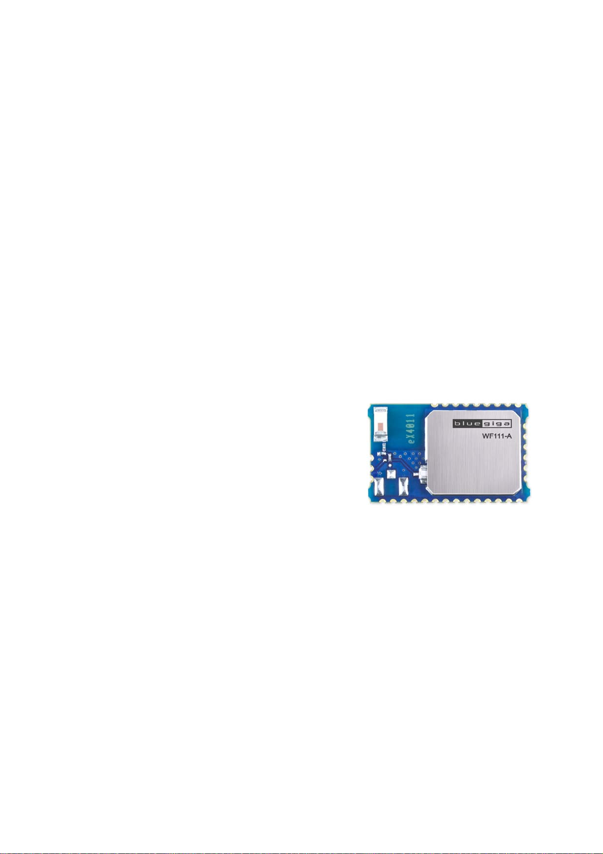
Figure 1: WF111-A
Bluegiga Technologies Oy

2 Ordering Information
WF111 Product Numbering
WF1 1 1- X
Antenna:
A = Internal antenna
E = External
N = RF pin
Confirmed products and codes
Product code Description
WF111-A WF111 module with internal chip antenna
WF111-E WF111 module with U.FL connector for external antenna
WF111-N WF111 module with 50 RF pin (contact sales@bluegiga.com for availability)
DKWF111 WF111-A SDIO evaluation kit
Bluegiga Technologies Oy
Page 7 of 47

3 Pinout and terminal descriptions
29
28
27
26
25
24
23
22
21
30
31
32
33
GND
ANT
GND
GND_PAD
GND
1
SDIO_DAT[1]
SDIO_DAT[0]
3
2
SDIO_DAT[3]
SDIO_DAT[2]
5
4
GND
SDIO_CLK
7
6
PIO[5]
VDD_PA
GND
SDIO_CMD
8
SPI_CS
BT
9
Figure 2: WF111 pinout
10
RST
VDD_ANA
PIO[1]
SPI_MISO
11
12
REGEN
SPI_CLK
PIO[0]
VDD_PADS
VDD_REGIN
VDD_SDIO
SPI_MOSI
14
13
GND
PIO[3]
PIO[4]
PIO[2]
GND
20
19
18
17
16
15
Bluegiga Technologies Oy
Page 8 of 47

POWER
SUPPLIES
PIN NUMBER DESCRIPTION
VDD_REGIN 17 Input for the internal regulators
REGEN 23 Pull high to enable internal voltage regulators (2.0V max )
GND
1, 8, 14, 21,
29, 30, 32
Ground
GND_PAD 33 Thermal pad, on bottom of WF111
VDD_ANA 10 Positive supply for PA control
VDD_PADS 19 Positive supply for the digital interfaces
VDD_SDIO 15 Positive supply for the SDIO interface
VDD_PA 28 Positive supply for the power amplifier
Table 1: Supply Terminal Descriptions
PIO
PORT
PIN
NUMBER
PAD TYPE DESCRIPTION
PIO[0] 22
PIO[1] 24
PIO[2] 16
PIO[3] 20
PIO[4] 18
PIO[5] 27
Bi-directional, programmable strength
internal pull-down/pull-up
Table 2: GPIO Terminal Descriptions
Programmable input/output
line.
Can be used for Bluetooth coexistence.
Bluegiga Technologies Oy
Page 9 of 47

SDIO/CSPI
Interfaces
SDIO_DATA[0]
SDIO_SPI_DI SDIO SPI data output
CSPI_MISO CSPI data output
SDIO_DATA[1]
SDIO_SPI_INT SDIO SPI interrupt output
PIN
NUMBER
2
3
PAD TYPE DESCRIPTION
Synchronous data input/output
Bi-directional, tristate, weak
internal pull-up
Synchronous data input/output
CSPI_INT CSPI data input
SDIO_DATA[2] 4 Synchronous data input/output
SDIO_DATA[3]
SDIO_SPI_CS# SDIO SPI chip select, active low
5
CSPI_CS# CSPI chip select, active low
Bi-directional,
weak/strong
internal pull-up
SDIO_CLK
SDIO_SPI_SCLK SDIO SPI clock
6
Input, weak
internal pull-up
Synchronous data input/output
SDIO clock
CSPI_CLK CSPI clock
SDIO_CMD
SDIO_SPI_MOSI SDIO SPI data input
7
CSPI_MOSI CSPI data input
Bi-directional,
weak internal
pull-up
SDIO data input
Table 3: Host Interface Terminal Descriptions
Bluegiga Technologies Oy
Page 10 of 47

OTHER
SIGNALS
RST 25
ANT 31 RF, DC blocked
PIN
NUMBER
PAD TYPE DESCRIPTION
Input, weak internal pullup, active low
System reset
Antenna output on N variant, on A
and E variants not connected
BT 9 RF, DC blocked Bluetooth antenna sharing RF input
Table 4: Other Terminal Descriptions
DEBUG SPI
INTERFACE
SPI_MISO 11
SPI_CLK 12
SPI_MOSI 13 Synchronous data input
PIN
NUMBER
PAD TYPE DESCRIPTION
Output, tri-state, weak
internal pull-down
Synchronous data output
Synchronous clock input
Input, weak internal
pull-down
SPI_CS 26 Debug SPI Chip select, active low
Table 5: Debug SPI Terminal Descriptions
Bluegiga Technologies Oy
Page 11 of 47

4 Interfaces
4.1 Host interfaces
WF111 can be interfaced by the host using SDIO in 1bit or 4bit mode, SDIO SPI or CSR proprietary CSPI
connection. The host connection buses can be clocked up to 50MHz.
4.1.1 Host selection
WF111 will default to 1-bit SDIO mode. The host interface can be set with 1-bit SDIO or SDIO SPI commands
to the required mode. After mode selection, it will then remain in that mode until the module is reset either with
the RESET pin or the internal power supply supervisor.
4.1.2 SDIO interface
This is a host interface which allows a Secure Digital Input Output (SDIO) host to gain access to the internals
of the chip. All defined slave modes (SPI, SD 1bit, SD 4bit) are provided.
Two functions are supported:
Function 0 is mandatory function used for SDIO slave configuration. This contains CCCR, FBR and
CIS. CCCR registers support sleep and wakeup signaling.
Function 1 provides access to the IEEE 802.11 functionality. Command IO_RW_DIRECT (CMD52) is
used to directly access internal registers. IO_RW_EXTENDED (CMD53) is used for block transfer
to/from module MMU buffers.
Command SD Mode (1/4 bit) SDIO SPI Mode
GO_IDLE_STATE (CMD0) Y Y
SEND_RELATIVE_ADDR (CMD3) Y N
IO_SEND_OP_COND (CMD5) Y Y
SELECT/DESELECT_CARD (CMD7) Y N
GO_INACTIVE_STATE (CMD15) Y N
IO_RW_DIRECT (CMD52) Y Y
IO_RW_EXTENDED (CMD53) Y Y
CRC_ON_OFF (CMD59) N Y
Table 6: Supported commands per mode
For more information and detailed descriptions of above functions and commands, see the following
specifications:
SD Specifications Part 1 Physical Layer Specification v.1.10
SD Specification Part E1 SDIO Specification v.1.10
Bluegiga Technologies Oy
Page 12 of 47
4.1.3 CSR Serial Peripheral Interface (CSPI)
The CSPI is a host interface which shares pins with the SDIO. It contains a number of modifications on the
SDIO SPI specification aimed at increasing the host bus efficiency in hosts supporting SPI but not SDIO. The
main advantages compared to SDIO SPI are:
Burst transfer is continuous instead of blocks with CRC
Timings are deterministic (fixed number of clocks) reducing the required interaction
16 bit registers are transferred as a single command instead of two 8 bit writes
MMU buffers are accessed using burst read/writes. The command and address fields are used to select the
correct buffer. The CSPI is able to generate an interrupt to the host when a memory access fails. This
interrupt line is shared with the SDIO functions.
The CSPI Interface is an extension of the basic SPI Interface, with the access type determined by the
following fields:
8-bit command
24-bit address
16-bit burst length (optional). Only applicable for burst transfers into or out of the MMU
4.1.3.1 CSPI read/write cycles
Register read/write cycles are used to access Function 0, Bluetooth acceleration and MCU registers.
Burst read/write cycles are used to access the MMU.
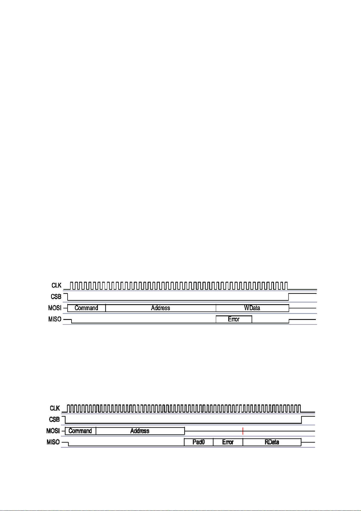
4.1.3.2 CSPI register write cycle
The command and address are locked into the slave, followed by 16bits of write data. An Error Byte is
returned on the MISO signal indicating whether or not the transfer has been successful.
Figure 3: CSPI Register Write Cycle
4.1.3.3 CSPI register read cycle
The command and address field are clocked into the slave, the slave then returns the following:
Bytes of padding data (MISO held low)
Error byte
16-bits of read data
Figure 4: CSPI Register Read Cycle
Bluegiga Technologies Oy
Page 13 of 47
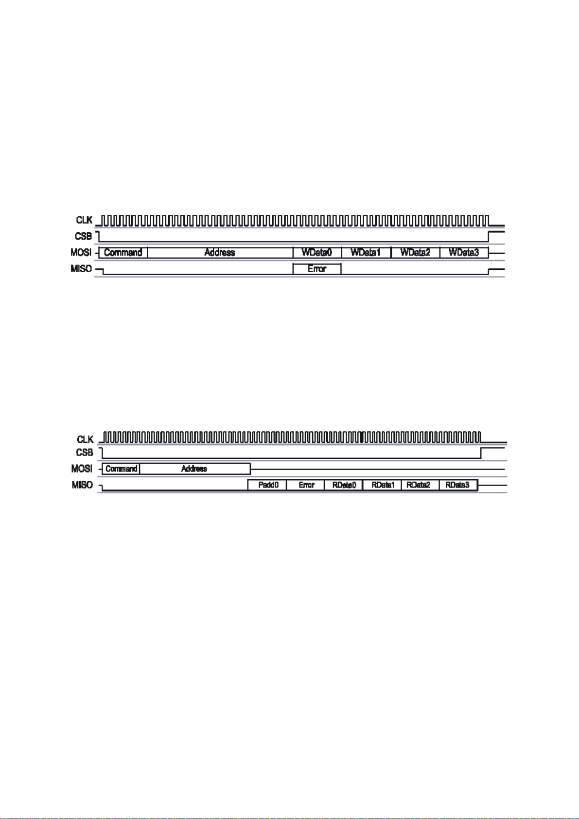
4.1.3.4 CSPI register burst write cycle
Burst transfers are used to access the MMU buffers. They cannot be used to access registers. Burst
read/write cycles are selected by setting the nRegister/Burst bit in the command field to 1.
Burst transfers are byte orientated, have a minimum length of 0 bytes and a maximum length of 64kbytes.
Setting the length field to 0 results in no data being transferred to or from the MMU.
As with a register access, the command and address fields are transferred first. There is an optional length
field transferred after the address. The use of the length field is controlled by the LengthFieldPresent bit in the
Function 0 registers, which is cleared on reset.
Figure 5: CSPI Burst Write Cycle
4.1.3.5 CSPI register read cycle
Burst reads have a programmable amount of padding data that is returned by the slave. 0-15 bytes are
returned as defined in the BurstPadding register. Following this the Error byte is returned followed by the data.
Once the transfer has started, no further padding is needed.
A FIFO within SDIO_TOP will pre-fetch the data. The address is not retransmitted, and is auto-updated within
the slave.
The length field is transmitted if LengthFieldPresent in the Function 0 registers is set. In the absence of a
length field the CSB signal is used to indicate the end of the burst.
Figure 6: CSPI Burst Read Cycle
Bluegiga Technologies Oy
Page 14 of 47

4.1.4 SDIO/CSPI deep-sleep control schemes
The module automatically enters deep sleep to minimize power consumption after a while of idling. Deep
sleep is the lowest power mode, where the processor, the internal reference (fast) clock, and much of the
digital and analogue hardware are shut down. The SDIO communication system however remains on, and is
clocked by the host system. During deep sleep only the function 0 is available, while attempts to access
Function 1 will likely result in bus timeouts.
Control of when the module is allowed to enter deep sleep is done via Vendor Unique Register in CCCR in
function 0. Wake-up is also initiated through this register. The module will initiate an SDIO interrupt when the
wake-up is complete.
Bluegiga Technologies Oy
Page 15 of 47
 Loading...