

BGM210P Blue Gecko Bluetooth Module
Data Sheet
The BGM210P is a module designed and built to meet the performance, security, and reliability requirements of line-powered
IoT products for Bluetooth networks.
Based on the EFR32BG21 SoC, it enables Bluetooth® Low Energy and Bluetooth Mesh
connectivity while delivering best-in-class RF range and performance, future-proof capability for feature and OTA firmware updates, enhanced security, low active current consumption, and a temperature rating suited for operating in demanding environmental
conditions.
The BGM210P is a complete solution that comes with robust and fully-upgradeable software stacks, world-wide regulatory certifications, advanced development and debugging
tools, and support that will simplify and minimize the development cycle and deployment
of your end-product helping to accelerate its time-to-market.
The BGM210P is targeted for a broad range of applications, including:
• Smart home
• Connected lighting
• Building automation and security
• Factory automation
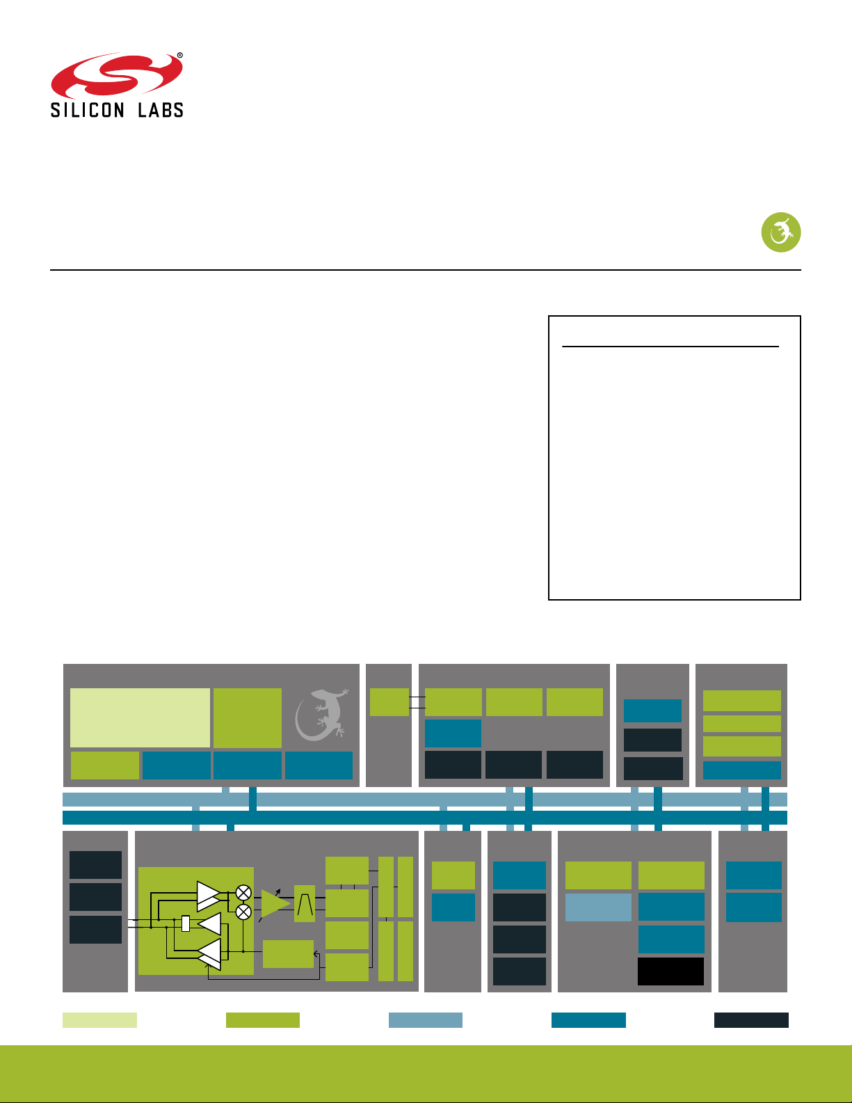
Core / Memory
ARM Cortex
TM
M33 processor
with DSP extensions,
FPU and TrustZone
ETM Debug Interface RAM Memory
Flash Program
Memory
LDMA
Controller
Crystal
38.4
MHz
HF Crystal
Oscillator
EM23 HF RC
Oscillator
LF Crystal
Oscillator
HF
RC Oscillator
Ultra LF RC
Oscillator
KEY FEATURES
• Bluetooth 5.1 and Bluetooth Mesh
connectivity
• Chip antenna and RF pin
• +10 and +20 dBm TX power variants
• -97.0 dBm Bluetooth RX sensitivity at 1
Mbps
• 32-bit ARM Cortex-M33 core at 38.4 MHz
• 1024/96 kB of Flash/RAM memory
• Enhanced security features
• Optimal set of MCU peripherals
• 20 GPIO pins
•
-40 to +125 oC
• 12.9 mm x 15.0 mm x 2.2 mm
Fast Startup
RC Oscillator
LF
RC Oscillator
Energy
Management
Voltage
Regulator
Brown-Out
Detector
Power-On
Reset
SecurityClock Management
Crypto
Acceleration
Secure Debug
True Random
Number Generator
Security Core
32-bit bus
Peripheral Reflex System
Antenna
Chip
Antenna
Matching
RF Pin
Lowest power mode with peripheral operational:
RF Frontend
Radio Transceiver
I
LNA
Q
PA
PA
PGA
Frequency
Synth
DEMOD
IFADC
AGC
MOD
FRC
CRC
BUFC
RAC
Serial
Interfaces
USART
2
I
C
I/O Ports Analog I/F
External
Interrupts
General
Purpose I/O
Pin Reset
Pin Wakeup
Timers and Triggers
Timer/Counter
Low Energy
Timer
EM3—StopEM2—Deep SleepEM1—SleepEM0—Active
Protocol Timer
Watchdog Timer
Real Time
Capture Counter
Back-Up Real
Time Counter
ADC
Analog
Comparator
EM4—Shutoff
silabs.com | Building a more connected world. Rev. 0.5

1. Features
BGM210P Blue Gecko Bluetooth Module Data Sheet
Features
• Supported Protocols
• Bluetooth 5.1
• Bluetooth Low Energy
• Bluetooth Mesh
• AoA/AoD
• Wireless System-on-Chip
• 2.4 GHz radio
• TX power up to +20 dBm
•
High-performance 32-bit ARM Cortex-M33® with DSP instruction and floating-point unit for efficient signal processing
• 1024 kB flash program memory
• 96 kB RAM data memory
• Embedded Trace Macrocell (ETM) for advanced debugging
• Receiver Performance
• -104.5 dBm sensitivity (0.1% BER) at 125 kbps GFSK
• -100.1 dBm sensitivity (0.1% BER) at 500 kbps GFSK
• -97.0 dBm sensitivity (0.1% BER) at 1 Mbps GFSK
• -94.1 dBm sensitivity (0.1% BER) at 2 Mbps GFSK
• Current Consumption
• 9.3 mA RX current at 1 Mbps GFSK
• 16.1 mA TX current at 0 dBm (BGM210Px22)
• 34.1 mA TX current at 10 dBm (BGM210Px22)
• 173 mA TX current at 20 dBm (BGM210Px32)
• 50.9µA/MHz in Active Mode (EM0)
• 5.1μA EM2 DeepSleep current (RTCC running from LFXO,
Bluetooth Stack not running)
• 8.5μA EM2 DeepSleep current (RTCC running from LFXO,
Bluetooth Stack running)
• Regulatory Certifications
• CE
• ISED
• FCC
• Operating Range
• 1.8 to 3.8 V
• -40 to +125 °C
• Dimensions
• 12.9 mm x 15.0 mm x 2.2 mm
• Security
•
Secure Boot with Root of Trust and Secure Loader (RTSL)
• Hardware Cryptographic Acceleration with DPA countermeasures1 for AES128/256, SHA-1, SHA-2 (up to 256-bit),
ECC (up to 256-bit), ECDSA, and ECDH
• True Random Number Generator (TRNG) compliant with
NIST SP800-90 and AIS-31
•
ARM® TrustZone
®
• Secure Debug Interface lock/unlock
• MCU Peripherals
• 12-bit 1 Msps SAR Analog to Digital Converter (ADC)
• 2 × Analog Comparator (ACMP)
• 20 General Purpose I/O pins with output state retention and
asynchronous interrupts
• 8 Channel DMA Controller
• 12 Channel Peripheral Reflex System (PRS)
• 2 × 16-bit Timer/Counter
(3 Compare/Capture/PWM channels)
• 1 × 32-bit Timer/Counter
(3 Compare/Capture/PWM channels)
• 32-bit Real Time Counter
• 24-bit Low Energy Timer for waveform generation
• 2 × Watchdog Timer
• 3 × Universal Synchronous/Asynchronous Receiver/Transmitter (UART/SPI/SmartCard (ISO 7816)/IrDA/I2S)
•
2 × I2C interface with SMBus support
1
1. With Secure Element (SE) firmware v1.1.2 or newer
silabs.com | Building a more connected world. Rev. 0.5 | 2

2. Ordering Information
BGM210P Blue Gecko Bluetooth Module Data Sheet
Ordering Information
Table 2.1. Ordering Information
Ordering Code Protocol Stack TX Power Freq Band Antenna
1
BGM210P022JIA2
• Bluetooth 5.1 10 dBm 2.4 GHz Chip and
RF pin
1
BGM210P022JIA2R
• Bluetooth 5.1 10 dBm 2.4 GHz Chip and
RF pin
1
BGM210P032JIA2
• Bluetooth 5.1 20 dBm 2.4 GHz Chip and
RF pin
1
BGM210P032JIA2R
• Bluetooth 5.1 20 dBm 2.4 GHz Chip and
RF pin
2
BGM210PA22JIA2
• Bluetooth 5.1 10 dBm 2.4 GHz Chip and
RF pin
2
BGM210PA22JIA2R
• Bluetooth 5.1 10 dBm 2.4 GHz Chip and
RF pin
2
BGM210PA32JIA2
• Bluetooth 5.1 20 dBm 2.4 GHz Chip and
RF pin
2
BGM210PA32JIA2R
• Bluetooth 5.1 20 dBm 2.4 GHz Chip and
RF pin
1. Engineering sample device
2. Production device
Flash
(kB)
RAM
(kB) GPIO Temp Range Packaging
1024 96 20 -40 to 125 °C Cut Tape
1024 96 20 -40 to 125 °C Reel
1024 96 20 -40 to 125 °C Cut Tape
1024 96 20 -40 to 125 °C Reel
1024 96 20 -40 to 125 °C Cut Tape
1024 96 20 -40 to 125 °C Reel
1024 96 20 -40 to 125 °C Cut Tape
1024 96 20 -40 to 125 °C Reel
See 4.5 RF Transmitter General Characteristics for maximum TX power figures.
End-product manufacturers must verify that the module is configured to comply with the regulatory limits for each region, in accordance
with the formal certification test reports for the device.
BGM210P modules are pre-programmed with BGAPI UART DFU bootloader.
Throughout this document, the devices above may be referred to by their product family name (BGM210P), model name
(BGM210P22A / BGM210P32A) or full ordering code.
The SLWSTK6102A Wireless Gecko Module Starter Kit is available for BGM210P evaluation and development, as well as
SLWRB4308A (+20 dBm TX) and SLWRB4308B (+10 dBm TX) radio boards.
silabs.com | Building a more connected world. Rev. 0.5 | 3

Table of Contents
1. Features .................................2
2. Ordering Information ............................3
3. System Overview ..............................6
3.1 Block Diagram ..............................6
3.2 EFR32BG21 SoC .............................6
3.3 Antenna ................................6
3.4 Power Supply ..............................6
4. Electrical Specifications ...........................7
4.1 Absolute Maximum Ratings..........................7
4.2 General Operating Conditions .........................8
4.3 MCU Current Consumption at 3.0V .......................9
4.4 Radio Current Consumption at 3.0V .......................10
4.5 RF Transmitter General Characteristics .....................11
4.6 RF Receiver General Characteristics ......................12
4.7 RF Receiver Characteristics for Bluetooth Low Energy at 1 Mbps .............13
4.8 RF Receiver Characteristics for Bluetooth Low Energy at 2 Mbps .............14
4.9 RF Receiver Characteristics for Bluetooth Low Energy at 500 kbps ............15
4.10 RF Receiver Characteristics for Bluetooth Low Energy at 125 kbps ............16
4.11 High-Frequency Crystal ..........................17
4.12 GPIO Pins ...............................18
4.13 Microcontroller Peripherals .........................19
4.14 Typical Performance Curves .........................19
4.14.1 Antenna Radiation and Efficiency ......................20
5. Reference Diagrams............................ 21
5.1 Network Co-Processor (NCP) Application with UART Host ...............21
5.2 SoC Application .............................22
6. Pin Definitions ..............................23
6.1 Module Pinout ..............................23
6.2 Alternate Pin Functions ...........................24
6.3 Analog Peripheral Connectivity ........................24
6.4 Digital Peripheral Connectivity .........................25
7. Design Guidelines ............................28
7.1 Layout and Placement ...........................28
7.2 Proximity to Other Materials .........................30
7.3 Proximity to Human Body ..........................30
silabs.com
| Building a more connected world. Rev. 0.5 | 4

8. Package Specifications ..........................31
8.1 Dimensions ...............................31
8.2 PCB Land Pattern .............................32
8.3 Package Marking .............................33
9. Soldering Recommendations ........................34
10. Tape and Reel .............................35
11. Certifications ..............................36
11.1 Qualified Antennas ............................36
11.2 CE .................................36
11.3 FCC .................................36
11.4 ISED Canada ..............................39
11.5 Proximity to Human Body ..........................41
12. Revision History............................. 42
silabs.com | Building a more connected world. Rev. 0.5 | 5
BGM210P Blue Gecko Bluetooth Module Data Sheet
System Overview
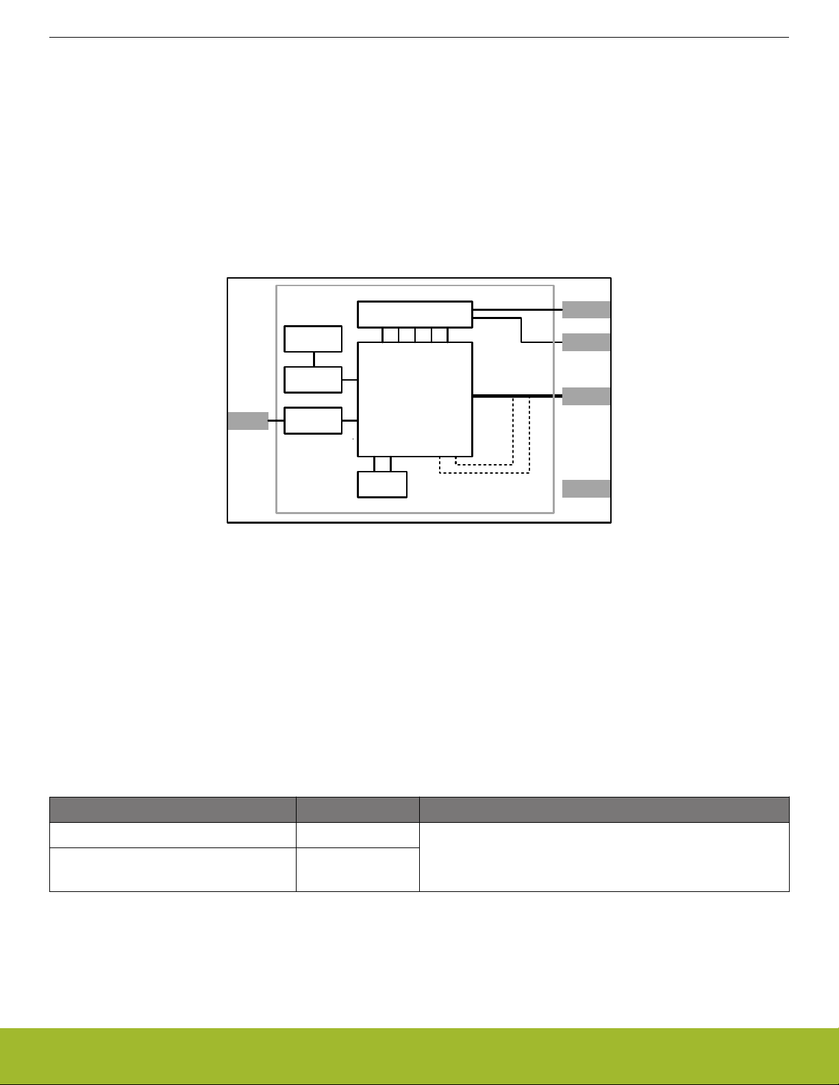
3. System Overview
3.1 Block Diagram
The BGM210P module is a highly-integrated, high-performance system with all the hardware components needed to enable 2.4 GHz
wireless connectivity and to support robust networking capabilities via multiple protocols.
Built around the EFR32BG21 Wireless Gecko SoC, the BGM210P includes a chip antenna, an RF matching network (optimized for
transmit power efficiency), supply decoupling and filtering components, a 38.4 MHz reference crystal, and an RF shield. It also comes
with a 50 Ω-matched RF pin and allows the use of an external 32 kHz crystal as a low frequency reference signal via GPIO pins.
Since the RF matching networks are optimized for transmit power efficiency, modules rated for +20 dBm will show non-optimal current
consumption and performance when operated at a lower output power (e.g. +10 or 0 dBm). The same applies for modules rated for +10
dBm.
VDD
IOVDD
GPIO
Antenna
RF Match
Supply Decoupling
Silicon Labs
(up to 20)
EFR32BG21
RFPIN
3.2 EFR32BG21 SoC
The EFR32BG21 SoC features a 32-bit ARM Cortex M33 core, a 2.4 GHz high-performance radio, 1 MB of Flash memory, a dedicated
core for security, a rich set of MCU peripherals, and various clock management and serial interfacing options. Consult the EFR32xG21
Wireless Gecko Reference Manual and the EFR32BG21 Data Sheet for details.
3.3 Antenna
BGM210P modules include a ceramic chip antenna on board with the characteristics detailed in the table below. They also include a 50
Ω-matched RF pin to enable the use of an external antenna instead of the module's chip antenna. See 4.14.1 Antenna Radiation and
Efficiency and 11.1 Qualified Antennas for other relevant details.
RF Match
HF XTAL
External LF XTAL option
Figure 3.1. BGM210P Block Diagram
RF SHIELD
GND
Table 3.1. Antenna Efficiency and Peak Gain
Parameter With optimal layout Note
Efficiency -1 to -2 dB Antenna efficiency, gain and radiation pattern are highly depend-
Peak gain 1.86 dBi
ent on the application PCB layout and mechanical design. Refer
to Design Guidelines for recommendations to achieve optimal antenna performance.
3.4 Power Supply
The BGM210P requires a single nominal supply level of 3.0 V to operate. However, it can support use cases needing different levels for
the main supply (VDD) and for digital IO (IOVDD). All necessary decoupling and filtering components are included in the module.
silabs.com | Building a more connected world. Rev. 0.5 | 6

BGM210P Blue Gecko Bluetooth Module Data Sheet
Electrical Specifications
4. Electrical Specifications
All electrical parameters in all tables are specified under the following conditions, unless stated otherwise:
• Typical values are based on TA=25 °C and VDD supply at 3.0 V, by production test and/or technology characterization.
• Radio performance numbers are measured in conducted mode, based on Silicon Laboratories reference designs using output power-specific external RF impedance-matching networks for interfacing to a 50 Ω antenna.
• Minimum and maximum values represent the worst conditions across supply voltage, process variation, and operating temperature,
unless stated otherwise.
4.1 Absolute Maximum Ratings
Stresses above those listed below may cause permanent damage to the device. This is a stress rating only and functional operation of
the devices at those or any other conditions above those indicated in the operation listings of this specification is not implied. Exposure
to maximum rating conditions for extended periods may affect device reliability. For more information on the available quality and reliability data, see the Quality and Reliability Monitor Report at http://www.silabs.com/support/quality/pages/default.aspx.
Table 4.1. Absolute Maximum Ratings
Parameter Symbol Test Condition Min Typ Max Unit
Storage temperature range T
Voltage on any supply pin V
Voltage ramp rate on VDD
supply pin
DC voltage on any GPIO pin V
Total current into VDD power
lines
Total current into GND pin I
Current per I/O pin I
Current for all I/O pins I
STG
DDMAX
V
DDRAMPMAX
DIGPIN
I
VDDMAX
GNDMAX
IOMAX
IOALLMAX
-50 — +150 °C
-0.3 — 3.8 V
— — 1.0 V / µs
-0.3 — V
IOVDD
+
V
0.3
Source — — 200 mA
Sink — — 200 mA
Sink — — 50 mA
Source — — 50 mA
Sink — — 200 mA
Source — — 200 mA
silabs.com | Building a more connected world. Rev. 0.5 | 7

BGM210P Blue Gecko Bluetooth Module Data Sheet
Electrical Specifications
4.2 General Operating Conditions
This table specifies the general operating temperature range and supply voltage range for all supplies. The minimum and maximum
values of all other tables are specifed over this operating range, unless otherwise noted.
Table 4.2. General Operating Conditions
Parameter Symbol Test Condition Min Typ Max Unit
Operating ambient tempera-
T
A
-I temperature grade -40 — +125 ° C
ture range
VDD Supply Voltage V
IOVDD operating supply volt-
DD
V
IOVDD
1.8 3.0 3.8 V
1.8 3.0 3.8 V
age (All IOVDD pins)
HCLK and Core frequency f
PCLK frequency f
EM01 Group A clock fre-
HCLK
PCLK
f
EM01GRPACLK
MODE = WS1, RAMWSEN = 1
MODE = WS1, RAMWSEN = 0
MODE = WS0, RAMWSEN = 0
1
1
1
— — 80 MHz
— — 50 MHz
— — 39 MHz
— — 50 MHz
— — 80 MHz
quency
HCLK Radio frequency f
HCLKRADIO
38 38.4 40 MHz
Note:
1. Flash wait states are set by the MODE field in the MSC_READCTRL register. RAM wait states are enabled by setting the RAMW-
SEN bit in the SYSYCFG_DMEM0RAMCTRL register.
silabs.com | Building a more connected world. Rev. 0.5 | 8

BGM210P Blue Gecko Bluetooth Module Data Sheet
Electrical Specifications
4.3 MCU Current Consumption at 3.0V
Unless otherwise indicated, typical conditions are: VDD = 3.0 V. TA = 25 °C. Minimum and maximum values in this table represent the
worst conditions across process variation at TA = 25 °C.
Table 4.3. MCU Current Consumption at 3.0V
Parameter Symbol Test Condition Min Typ Max Unit
Current consumption in EM0
mode with all peripherals dis-
1
abled
Current consumption in EM1
mode with all peripherals dis-
1
abled
Current consumption in EM2
mode
Current consumption in EM3
mode
I
ACTIVE
I
EM1
I
EM2
I
EM3
80 MHz HFRCO, CPU running
— 50.9 — µA/MHz
Prime from flash
80 MHz HFRCO, CPU running
— 45.6 55.5 µA/MHz
while loop from flash
80 MHz HFRCO, CPU running
— 59.8 — µA/MHz
CoreMark loop from flash
38.4 MHz crystal, CPU running
— 63.8 — µA/MHz
while loop from flash
80 MHz HFRCO — 28.7 37.6 µA/MHz
38.4 MHz crystal — 46.9 — µA/MHz
Full RAM retention and RTC run-
— 5.1 — µA
ning from LFXO (Bluetooth Stack
not running)
Full RAM retention, RTCC run-
— 8.5 — µA
ning, and Bluetooth Stack running
from LFXO
1 bank (16 kB) RAM retention and
— 4.5 10.5 µA
RTC running from LFRCO
Full RAM retention and RTC run-
— 4.8 11.4 µA
ning from ULFRCO
1 bank (16 kB) RAM retention and
— 4.3 — µA
RTC running from ULFRCO
Current consumption in EM4
I
EM4
No BURTC, no LF oscillator — 0.21 0.5 µA
mode
Current consumption during
I
RST
Hard pin reset held — 146 — µA
reset
Current consumption per re-
I
RAM
— 0.10 — µA
tained 16kB RAM bank in
EM2
Note:
1. The typical EM0/EM1 current measurement includes some current consumed by the security core for periodical housekeeping
purposes. This does not include current consumed by user-triggered security operations, such as cryptographic calculations.
silabs.com | Building a more connected world. Rev. 0.5 | 9

BGM210P Blue Gecko Bluetooth Module Data Sheet
Electrical Specifications
4.4 Radio Current Consumption at 3.0V
RF current consumption measured with MCU in EM1, HCLK = 38.4 MHz, and all MCU peripherals disabled. Unless otherwise indicated, typical conditions are: VDD = 3.0V. TA = 25 °C. Minimum and maximum values in this table represent the worst conditions across
process variation at TA = 25 °C.
Table 4.4. Radio Current Consumption at 3.0V
Parameter Symbol Test Condition Min Typ Max Unit
Current consumption in receive mode, active packet
reception
Current consumption in receive mode, Stack running
Current consumption in
transmit mode
I
RX_ACTIVE
I
RX_LISTEN
I
TX
125 kbit/s, 2GFSK, f = 2.4 GHz,
Bluetooth stack running
500 kbit/s, 2GFSK, f = 2.4 GHz,
Bluetooth stack running
1 Mbit/s, 2GFSK, f = 2.4 GHz,
Bluetooth stack running
2 Mbit/s, 2GFSK, f = 2.4 GHz,
Bluetooth stack running
125 kbit/s, 2GFSK, f = 2.4 GHz,
Bluetooth stack running
500 kbit/s, 2GFSK, f = 2.4 GHz,
Bluetooth stack running
1 Mbit/s, 2GFSK, f = 2.4 GHz,
Bluetooth stack running
2 Mbit/s, 2GFSK, f = 2.4 GHz,
Bluetooh stack running
f = 2.4 GHz, CW, 10 dBm Module,
0 dBm output power
f = 2.4 GHz, CW, 10 dBm Module,
10 dBm output power
— 9.3 — mA
— 9.3 — mA
— 9.3 — mA
— 9.9 — mA
— 9.1 — mA
— 9.1 — mA
— 9.1 — mA
— 9.8 — mA
— 16.1 — mA
— 34.1 — mA
f = 2.4 GHz, CW, 20 dBm Module,
10 dBm output power, VDD = 3.0
V
f = 2.4 GHz, CW, 20 dBm Module,
P
=19.2 dBm, VDD = 3.3 V
OUT
Note:
1. The maximum power for Bluetooth Low-Energy is limited to 19.2 dBm.
— 59.7 — mA
— 173 — mA
1
silabs.com | Building a more connected world. Rev. 0.5 | 10

BGM210P Blue Gecko Bluetooth Module Data Sheet
Electrical Specifications
4.5 RF Transmitter General Characteristics
Unless otherwise indicated, typical conditions are: TA = 25 °C, VDD = 3.0V. Measured with RF center frequency of 2.45 GHz on
RF2G4_IO2 port.
Table 4.5. RF Transmitter General Characteristics
Parameter Symbol Test Condition Min Typ Max Unit
RF tuning frequency range F
Maximum TX output power
1
RANGE
POUT
Minimum active TX Power POUT
Output power step size POUT
Output power variation vs
POUT
VDD supply voltage, Freq =
2450MHz
MAX
MIN
STEP
VAR_V
2400 — 2483.5 MHz
20 dBm Module, BLE, VDD =
2
3.3V
— 19.2 — dBm
10 dBm Module — 10 — dBm
20 dBm Module, VDD = 3.3 V — -20.5 — dBm
10 dBm Module — -19.3 — dBm
10 dBm Module, -5 dBm < P
OUT
<
— 1.5 — dB
0 dBm
10 dBm Module, 0 dBm < P
OUT
<
— 1.0 — dB
10 dBm
20 dBm Module, 0 dBm < P
OUT
<
— 0.7 — dB
5 dBm
20 dBm Module, 5 dBm < P
POUT
MAX
20 dBm Module, P
POUT
VDD swept from 3.0V
MAX
OUT
=
OUT
<
— 0.5 — dB
— 1.0 — dB
to 3.8V.
10 dBm Module, P
POUT
VDD swept from 1.8V
MAX
OUT
=
— 0.2 — dB
to 3.0V.
Output power variation vs
temperature, Freq =
2450MHz
POUT
VAR_T
20 dBm Module, P
POUT
, VDD = 3.3V, tempera-
MAX
OUT
=
ture swept from -40 to +125 °C.
10 dBm Module, P
POUT
, VDD = 3.0V, tempera-
MAX
OUT
=
— 1.5 — dB
— 0.3 — dB
ture swept from -40 to +125 °C.
Output power variation vs RF
frequency
POUT
VAR_F
20 dBm Module, P
POUT
, VDD = 3.3V, Freq.
MAX
OUT
=
— 0.2 — dB
swept from 2400 to 2483.5 MHz
10 dBm Module, P
POUT
, VDD = 3.0V, Freq.
MAX
OUT
=
— 0.2 — dB
swept from 2400 to 2483.5 MHz
Note:
1. Supported transmit power levels are determined by the ordering part number (OPN). Transmit power ratings for all devices covered in this data sheet can be found in the TX Power column of the Ordering Information Table.
2. The maximum power for Bluetooth Low-Energy.
silabs.com | Building a more connected world. Rev. 0.5 | 11

BGM210P Blue Gecko Bluetooth Module Data Sheet
Electrical Specifications
4.6 RF Receiver General Characteristics
Unless otherwise indicated, typical conditions are: TA = 25 °C, VDD = 3.0V. Measured with RF center frequency of 2.45 GHz on
RF2G4_IO2 port.
Table 4.6. RF Receiver General Characteristics
Parameter Symbol Test Condition Min Typ Max Unit
RF tuning frequency range F
RANGE
2400 — 2483.5 MHz
silabs.com | Building a more connected world. Rev. 0.5 | 12

BGM210P Blue Gecko Bluetooth Module Data Sheet
Electrical Specifications
4.7 RF Receiver Characteristics for Bluetooth Low Energy at 1 Mbps
Unless otherwise indicated, typical conditions are: TA = 25 °C, VDD = 3.0V. RF center frequency 2.45 GHz. Measured on RF2G4_IO2.
Table 4.7. RF Receiver Characteristics for Bluetooth Low Energy at 1 Mbps
Parameter Symbol Test Condition Min Typ Max Unit
Max usable receiver input
level
SAT Signal is reference signal, packet
length is 37 bytes
1
Sensitivity SENS Signal is reference signal, 37 byte
1
1
3
5
Signal to co-channel interfer-erC/I
N ± 1 Adjacent channel se-
C/I
lectivity
CC
1
payload
With non-ideal signals2
(see notes)1
Interferer is reference signal at +1
MHz offset1 4 3
Interferer is reference signal at -1
5
5
N ± 2 Alternate channel selectivity
C/I
MHz offset1 4 3
2
Interferer is reference signal at +2
MHz offset1 4 3
Interferer is reference signal at -2
5
5
N ± 3 Alternate channel selectivity
C/I
MHz offset1 4 3
3
Interferer is reference signal at +3
MHz offset1 4 3
Interferer is reference signal at -3
MHz offset1 4 3
5
— 10 — dBm
— -97.0 — dBm
— -96.7 — dBm
— +6.6 — dB
— -8.3 — dB
— -8.7 — dB
— -42.1 — dB
— -48.9 — dB
— -42.4 — dB
— -54.8 — dB
Selectivity to image frequen-cyC/I
IM
Interferer is reference signal at im-
— -42.1 — dB
age frequency with 1 MHz preci-
5
sion1
Selectivity to image frequency ± 1 MHz
C/I
IM_1
Interferer is reference signal at image frequency +1 MHz with 1
MHz precision1
5
Interferer is reference signal at im-
— -42.4 — dB
— -8.3 — dB
age frequency -1 MHz with 1 MHz
5
6
— -23 — dBm
Intermodulation performance IM
precision1
n = 3
Note:
1. 0.1% Bit Error Rate.
2. With non-ideal signals as specified in Bluetooth Test Specification RF-PHY.TS.5.0.1 section 4.7.1
3. Desired signal -67 dBm.
4. Desired frequency 2402 MHz ≤ Fc ≤ 2480 MHz.
5. With allowed exceptions.
6. As specified in Bluetooth Core specification version 5.1, Vol 6, Part A, Section 4.4
silabs.com | Building a more connected world. Rev. 0.5 | 13

BGM210P Blue Gecko Bluetooth Module Data Sheet
Electrical Specifications
4.8 RF Receiver Characteristics for Bluetooth Low Energy at 2 Mbps
Unless otherwise indicated, typical conditions are: TA = 25 °C, VDD = 3.0V. RF center frequency 2.45 GHz. Measured on RF2G4_IO2.
Table 4.8. RF Receiver Characteristics for Bluetooth Low Energy at 2 Mbps
Parameter Symbol Test Condition Min Typ Max Unit
Max usable receiver input
level
SAT Signal is reference signal, packet
length is 37 bytes
1
Sensitivity SENS Signal is reference signal, 37 byte
1
1
3
5
Signal to co-channel interfer-erC/I
N ± 1 Adjacent channel se-
C/I
lectivity
CC
1
payload
With non-ideal signals2
(see notes)1
Interferer is reference signal at +2
MHz offset1 4 3
Interferer is reference signal at -2
5
5
N ± 2 Alternate channel selectivity
C/I
MHz offset1 4 3
2
Interferer is reference signal at +4
MHz offset1 4 3
Interferer is reference signal at -4
5
5
N ± 3 Alternate channel selectivity
C/I
MHz offset1 4 3
3
Interferer is reference signal at +6
MHz offset1 4 3
Interferer is reference signal at -6
MHz offset1 4 3
5
— 10 — dBm
— -94.1 — dBm
— -93.9 — dBm
— +6.0 — dB
— -8.0 — dB
— -8.8 — dB
— -42.2 — dB
— -50.3 — dB
— -54.4 — dB
— -55.4 — dB
Selectivity to image frequen-cyC/I
IM
Interferer is reference signal at im-
— -8.0 — dB
age frequency with 1 MHz preci-
5
sion1
Selectivity to image frequency ± 1 MHz
C/I
IM_1
Interferer is reference signal at image frequency +2 MHz with 1
MHz precision1
5
Interferer is reference signal at im-
— -42.2 — dB
— +6.0 — dB
age frequency -2 MHz with 1 MHz
5
6
— -22.3 — dBm
Intermodulation performance IM
precision1
n = 3
Note:
1. 0.1% Bit Error Rate.
2. With non-ideal signals as specified in Bluetooth Test Specification RF-PHY.TS.5.0.1 section 4.7.1
3. Desired signal -67 dBm.
4. Desired frequency 2402 MHz ≤ Fc ≤ 2480 MHz.
5. With allowed exceptions.
6. As specified in Bluetooth Core specification version 5.1, Vol 6, Part A, Section 4.4
silabs.com | Building a more connected world. Rev. 0.5 | 14

BGM210P Blue Gecko Bluetooth Module Data Sheet
Electrical Specifications
4.9 RF Receiver Characteristics for Bluetooth Low Energy at 500 kbps
Unless otherwise indicated, typical conditions are: TA = 25 °C, VDD = 3.0V. RF center frequency 2.45 GHz. Measured on RF2G4_IO2.
Table 4.9. RF Receiver Characteristics for Bluetooth Low Energy at 500 kbps
Parameter Symbol Test Condition Min Typ Max Unit
Max usable receiver input
SAT Signal is reference signal, packet
level
Sensitivity SENS
Signal to co-channel interfer-erC/I
N ± 1 Adjacent channel se-
C/I
CC
1
lectivity
N ± 2 Alternate channel se-
C/I
2
lectivity
N ± 3 Alternate channel se-
C/I
3
lectivity
Selectivity to image frequen-cyC/I
IM
length is 37 bytes
Signal is reference signal
With non-ideal signals2
(see notes)1
1
1
1
3
Interferer is reference signal at +1
MHz offset1 4 3
5
Interferer is reference signal at -1
MHz offset1 4 3
5
Interferer is reference signal at +2
MHz offset1 4 3
5
Interferer is reference signal at -2
MHz offset1 4 3
5
Interferer is reference signal at +3
MHz offset1 4 3
5
Interferer is reference signal at -3
MHz offset1 4 3
5
Interferer is reference signal at image frequency with 1 MHz preci-
5
sion1
— 10 — dBm
— -100.1 — dBm
— -99.3 — dBm
— +2.1 — dB
— -9.0 — dB
— -9.5 — dB
— -44.4 — dB
— -51.9 — dB
— -44.3 — dB
— -58.3 — dB
— -44.4 — dB
Selectivity to image frequency ± 1 MHz
C/I
IM_1
Interferer is reference signal at image frequency +1 MHz with 1
MHz precision1
5
Interferer is reference signal at im-
— -44.3 — dB
— -9.0 — dB
age frequency -1 MHz with 1 MHz
precision1
5
Note:
1. 0.1% Bit Error Rate.
2. With non-ideal signals as specified in Bluetooth Test Specification RF-PHY.TS.5.0.1 section 4.7.1
3. Desired signal -72 dBm.
4. Desired frequency 2402 MHz ≤ Fc ≤ 2480 MHz.
5. With allowed exceptions.
silabs.com | Building a more connected world. Rev. 0.5 | 15

BGM210P Blue Gecko Bluetooth Module Data Sheet
Electrical Specifications
4.10 RF Receiver Characteristics for Bluetooth Low Energy at 125 kbps
Unless otherwise indicated, typical conditions are: TA = 25 °C, VDD = 3.0V. RF center frequency 2.45 GHz. Measured on RF2G4_IO2.
Table 4.10. RF Receiver Characteristics for Bluetooth Low Energy at 125 kbps
Parameter Symbol Test Condition Min Typ Max Unit
Max usable receiver input
SAT Signal is reference signal, packet
level
Sensitivity SENS
Signal to co-channel interfer-erC/I
N ± 1 Adjacent channel se-
C/I
CC
1
lectivity
N ± 2 Alternate channel se-
C/I
2
lectivity
N ± 3 Alternate channel se-
C/I
3
lectivity
Selectivity to image frequen-cyC/I
IM
length is 37 bytes
Signal is reference signal
With non-ideal signals2
(see notes)1
1
1
1
3
Interferer is reference signal at +1
MHz offset1 4 3
5
Interferer is reference signal at -1
MHz offset1 4 3
5
Interferer is reference signal at +2
MHz offset1 4 3
5
Interferer is reference signal at -2
MHz offset1 4 3
5
Interferer is reference signal at +3
MHz offset1 4 3
5
Interferer is reference signal at -3
MHz offset1 4 3
5
Interferer is reference signal at image frequency with 1 MHz preci-
5
sion1
— 10 — dBm
— -104.5 — dBm
— -104.2 — dBm
— +0.8 — dB
— -13.1 — dB
— -13.6 — dB
— -49.5 — dB
— -56.9 — dB
— -47.0 — dB
— -63.1 — dB
— -49.5 — dB
Selectivity to image frequency ± 1 MHz
C/I
IM_1
Interferer is reference signal at image frequency +1 MHz with 1
MHz precision1
5
Interferer is reference signal at im-
— -47.0 — dB
— -13.1 — dB
age frequency -1 MHz with 1 MHz
precision1
5
Note:
1. 0.1% Bit Error Rate.
2. With non-ideal signals as specified in Bluetooth Test Specification RF-PHY.TS.5.0.1 section 4.7.1
3. Desired signal -79 dBm.
4. Desired frequency 2402 MHz ≤ Fc ≤ 2480 MHz.
5. With allowed exceptions.
silabs.com | Building a more connected world. Rev. 0.5 | 16

BGM210P Blue Gecko Bluetooth Module Data Sheet
Electrical Specifications
4.11 High-Frequency Crystal
Table 4.11. High-Frequency Crystal
Parameter Symbol Test Condition Min Typ Max Unit
Crystal frequency f
HFXTAL
Initial calibrated accuracy ACC
Temperature drift DRIFT
HFXTAL
HFXTAL
Across specified temperature
range
— 38.4 — MHz
-10 — +10 ppm
-30 — +30 ppm
silabs.com | Building a more connected world. Rev. 0.5 | 17

BGM210P Blue Gecko Bluetooth Module Data Sheet
Electrical Specifications
4.12 GPIO Pins
Unless otherwise indicated, typical conditions are: VDD = 3.0 V.
Table 4.12. GPIO Pins
Parameter Symbol Test Condition Min Typ Max Unit
Leakage current I
Input low voltage
Input high voltage
1
1
Output low voltage V
Output high voltage V
GPIO rise time T
GPIO fall time T
LEAK_IO
V
IL
V
IH
OL
OH
GPIO_RISE
GPIO_FALL
MODEx = DISABLED, VDD =
— 1.9 — nA
1.71V
MODEx = DISABLED, VDD = 3.0
— 2.5 — nA
V
MODEx = DISABLED, VDD = 3.8
— — 200 nA
V TA = 125 °C
Any GPIO pin — — 0.3 * VDD V
Any GPIO pin 0.7 * VDD — — V
Sinking 20mA, VDD = 3.0 V — — 0.2 * VDD V
Sinking 8mA, VDD = 1.62 V — — 0.4 * VDD V
Sourcing 20mA, VDD = 3.0 V 0.8 * VDD — — V
Sourcing 8mA, VDD = 1.62 V 0.6 * VDD — — V
VDD = 3.0V, C
= 50pF, SLEW-
load
— 8.4 — ns
RATE = 4, 10% to 90%
VDD = 1.7V, C
= 50pF, SLEW-
load
— 13 — ns
RATE = 4, 10% to 90%
VDD = 3.0V, C
= 50pF, SLEW-
load
— 7.1 — ns
RATE = 4, 90% to 10%
VDD = 1.7V, C
= 50pF, SLEW-
load
— 11.9 — ns
RATE = 4, 90% to 10%
Pull up/down resistance
R
PULL
pull-up: MODEn = DISABLE
35 44 55 kΩ
2
DOUT=1, pull-down: MODEn =
WIREDORPULLDOWN DOUT =
0
Maximum filtered glitch width T
GF
MODE = INPUT, DOUT = 1 — 26 — ns
Note:
1. GPIO and RESETn input thresholds are proportional to the VDD supply.
2. GPIO and RESETn pull-ups connect to the VDD supply. Pull-downs on GPIO connect to VSS.
silabs.com | Building a more connected world. Rev. 0.5 | 18

BGM210P Blue Gecko Bluetooth Module Data Sheet
Electrical Specifications
4.13 Microcontroller Peripherals
The MCU peripherals set available in BGM210P modules includes:
• 12-bit 1 Msps ADC
• Analog Comparators
• 16-bit and 32-bit Timers/Counters
• 24-bit Low Energy Timer for waveform generation
• 32-bit Real Time Counter
• USART (UART/SPI/SmartCards/IrDA/I2S)
•
I2C peripheral interfaces
• 12 Channel Peripheral Reflex System
For details on their electrical performance, consult the relevant portions of Section 4 in the SoC's datasheet.
To learn which GPIO ports provide access to every peripheral, consult 6.3 Analog Peripheral Connectivity and 6.4 Digital Peripheral
Connectivity.
4.14 Typical Performance Curves
Typical performance curves indicate typical characterized performance under the stated conditions.
silabs.com | Building a more connected world. Rev. 0.5 | 19

BGM210P Blue Gecko Bluetooth Module Data Sheet
Electrical Specifications
4.14.1 Antenna Radiation and Efficiency
Typical BGM210P radiation patterns and efficiency for the on-board chip antenna under optimal operating conditions are plotted in the
figures that follow. Antenna gain and radiation patterns have a strong dependence on the size and shape of the application PCB the
module is mounted on, as well as on the proximity of any mechanical design to the antenna.
Figure 4.1. Typical 2D Antenna Radiation Patterns and Efficiency
Top Left: Phi 0o, Top Right: Phi 90o, Bottom Left: Theta 90o, Bottom Right: Radiation Efficiency vs Application Board GND Plane Width
silabs.com | Building a more connected world. Rev. 0.5 | 20

BGM210P Blue Gecko Bluetooth Module Data Sheet
Reference Diagrams
5. Reference Diagrams
5.1 Network Co-Processor (NCP) Application with UART Host
The BGM210P can be controlled over the UART interface as a peripheral to an external host processor. Typical power supply, programming/debug interface, and host interface connections are shown in the figure below. For more details, refer to AN958: Debugging
and Programming Interfaces for Custom Designs.
Figure 5.1. UART NCP Configuration
silabs.com | Building a more connected world. Rev. 0.5 | 21

BGM210P Blue Gecko Bluetooth Module Data Sheet
Reference Diagrams
5.2 SoC Application
The BGM210P can be used in a stand-alone SoC configuration without an external host processor. Typical power supply and programming/debug interface connections are shown in the figure below. For more details, refer to AN958: Debugging and Programming Inter-
faces for Custom Designs.
Figure 5.2. Stand-Alone SoC Configuration
Figure 5.3. Stand-Alone SoC Configuration with External Antenna
silabs.com | Building a more connected world. Rev. 0.5 | 22

6. Pin Definitions
6.1 Module Pinout
BGM210P Blue Gecko Bluetooth Module Data Sheet
Pin Definitions
Figure 6.1. BGM210P Module Pinout
The next table shows the BGM210P pinout and some general descriptions of pin functionality. For more information on the features
supported by each GPIO, see 6.3 Analog Peripheral Connectivity and 6.4 Digital Peripheral Connectivity.
Table 6.1. BGM210P Module Pin Definitions
Pin Name No. Description Pin Name No. Description
GND 1 PB01 2 GPIO
PB00 3 GPIO PA00 4 GPIO
PA01 5 GPIO PA02 6 GPIO
PA03 7 GPIO PA04 8 GPIO
PA05 9 GPIO PA06 10 GPIO
Decouple output for on-chip voltage
DECOUPLE 11
VDD 13 Power supply IOVDD 14 Digital IO power supply
PD04 15 GPIO PD03 16 GPIO
PD02 17 GPIO PD01 18 GPIO
regulator. An external decoupling capacitor is required at this pin.
GND 12
PD00 19 GPIO GND 20
PC00 21 GPIO PC01 22 GPIO
PC02 23 GPIO PC03 24 GPIO
PC04 25 GPIO PC05 26 GPIO
RESETn 27 Reset Pin GND 28
RF2G4_IO2 29 2.4 GHz RF input/output GND 30
GND 31
silabs.com | Building a more connected world. Rev. 0.5 | 23

BGM210P Blue Gecko Bluetooth Module Data Sheet
Pin Definitions
6.2 Alternate Pin Functions
Some pins support multiple functions through internal multiplexing in the SoC (e.g. debugging, wake-up, etc.). The following table
shows the functions available on each module pin. Refer to SoC's reference manual for more details.
Table 6.2. GPIO Alternate Functions Table
GPIO Alternate Function
PB01 GPIO.EM4WU3
PA01 GPIO.SWCLK
PA02 GPIO.SWDIO
PA03 GPIO.SWV GPIO.TDO GPIO.TRACEDATA0
PA04 GPIO.TDI GPIO.TRACECLK
PA05 GPIO.EM4WU0
PD02 GPIO.EM4WU9
PD01 LFXO.LFXTAL_I LFXO.LF_EXTCLK
PD00 LFXO.LFXTAL_O
PC00 GPIO.EM4WU6
PC05 GPIO.EM4WU7
6.3 Analog Peripheral Connectivity
Many analog resources are routable and can be connected to numerous GPIO's. The table below indicates which peripherals are avaliable on each GPIO port. When a differential connection is being used Positive inputs are restricted to the EVEN pins and Negative
inputs are restricted to the ODD pins. When a single ended connection is being used positive input is avaliable on all pins. See the
device Reference Manual for more details on the ABUS and analog peripherals.
Table 6.3. ABUS Routing Table
Peripheral Signal PA PB PC PD
EVEN ODD EVEN ODD EVEN ODD EVEN ODD
ACMP0 ana_neg Yes Yes Yes Yes Yes Yes Yes Yes
ana_pos Yes Yes Yes Yes Yes Yes Yes Yes
ACMP1 ana_neg Yes Yes Yes Yes Yes Yes Yes Yes
ana_pos Yes Yes Yes Yes Yes Yes Yes Yes
IADC0 ana_neg Yes Yes Yes Yes Yes Yes Yes Yes
ana_pos Yes Yes Yes Yes Yes Yes Yes Yes
silabs.com | Building a more connected world. Rev. 0.5 | 24

BGM210P Blue Gecko Bluetooth Module Data Sheet
Pin Definitions
6.4 Digital Peripheral Connectivity
Many digital resources are routable and can be connected to numerous GPIO's. The table below indicates which peripherals are avaliable on each GPIO port.
Table 6.4. DBUS Routing Table
Peripheral.Resource PORT
PA PB PC PD
ACMP0.DIGOUT Available Available Available Available
ACMP1.DIGOUT Available Available Available Available
CMU.CLKIN0 Available Available
CMU.CLKOUT0 Available Available
CMU.CLKOUT1 Available Available
CMU.CLKOUT2 Available Available
FRC.DCLK Available Available
FRC.DFRAME Available Available
FRC.DOUT Available Available
I2C0.SCL Available Available Available Available
I2C0.SDA Available Available Available Available
I2C1.SCL Available Available
I2C1.SDA Available Available
LETIMER0.OUT0 Available Available
LETIMER0.OUT1 Available Available
PRS.ASYNCH0 Available Available
PRS.ASYNCH1 Available Available
PRS.ASYNCH10 Available Available
PRS.ASYNCH11 Available Available
PRS.ASYNCH2 Available Available
PRS.ASYNCH3 Available Available
PRS.ASYNCH4 Available Available
PRS.ASYNCH5 Available Available
PRS.ASYNCH6 Available Available
PRS.ASYNCH7 Available Available
PRS.ASYNCH8 Available Available
PRS.ASYNCH9 Available Available
PRS.SYNCH0 Available Available Available Available
PRS.SYNCH1 Available Available Available Available
PRS.SYNCH2 Available Available Available Available
PRS.SYNCH3 Available Available Available Available
silabs.com | Building a more connected world. Rev. 0.5 | 25

BGM210P Blue Gecko Bluetooth Module Data Sheet
Pin Definitions
Peripheral.Resource PORT
PA PB PC PD
TIMER0.CC0 Available Available Available Available
TIMER0.CC1 Available Available Available Available
TIMER0.CC2 Available Available Available Available
TIMER0.CDTI0 Available Available Available Available
TIMER0.CDTI1 Available Available Available Available
TIMER0.CDTI2 Available Available Available Available
TIMER1.CC0 Available Available Available Available
TIMER1.CC1 Available Available Available Available
TIMER1.CC2 Available Available Available Available
TIMER1.CDTI0 Available Available Available Available
TIMER1.CDTI1 Available Available Available Available
TIMER1.CDTI2 Available Available Available Available
TIMER2.CC0 Available Available
TIMER2.CC1 Available Available
TIMER2.CC2 Available Available
TIMER2.CDTI0 Available Available
TIMER2.CDTI1 Available Available
TIMER2.CDTI2 Available Available
TIMER3.CC0 Available Available
TIMER3.CC1 Available Available
TIMER3.CC2 Available Available
TIMER3.CDTI0 Available Available
TIMER3.CDTI1 Available Available
TIMER3.CDTI2 Available Available
USART0.CLK Available Available Available Available
USART0.CS Available Available Available Available
USART0.CTS Available Available Available Available
USART0.RTS Available Available Available Available
USART0.RX Available Available Available Available
USART0.TX Available Available Available Available
USART1.CLK Available Available
USART1.CS Available Available
USART1.CTS Available Available
USART1.RTS Available Available
USART1.RX Available Available
USART1.TX Available Available
silabs.com | Building a more connected world. Rev. 0.5 | 26

BGM210P Blue Gecko Bluetooth Module Data Sheet
Pin Definitions
Peripheral.Resource PORT
PA PB PC PD
USART2.CLK Available Available
USART2.CS Available Available
USART2.CTS Available Available
USART2.RTS Available Available
USART2.RX Available Available
USART2.TX Available Available
silabs.com | Building a more connected world. Rev. 0.5 | 27

BGM210P Blue Gecko Bluetooth Module Data Sheet
Design Guidelines
7. Design Guidelines
7.1 Layout and Placement
For optimal performance of the BGM210P,
• Place the module aligned to the edge of the application PCB, as illustrated in the figures below.
• Leave the antenna clearance area void of any traces, components, or copper on all layers of the application PCB if you are going to
use the on-board chip antenna
• Antenna clearance area is not necessary if you are using an external antenna attached to the RF pin.
• For external antenna use cases, use a 50 Ω grounded coplanar transmission line to trace the signal from the RF pin to an external RF connector if applicable (see Figure 7.2 Recommended Layout for BGM210P Using External Antenna on page 29).
• A general rule is to use 50 Ω transmission lines where the length of the RF trace is longer than λ/16 at the fundamental frequency, which for 2.4 GHz is approximately 7.8 mm.
• A U.FL connector can be used in the host PCB for the connection to an external antenna. The use of a U.FL connector is also
recommended for conductive tests. The integrator must use a unique connector, such as a “reverse polarity SMA” or “reverse
thread SMA”, if detachable antenna is offered with the host chassis. This is especially required for the FCC and ISED approvals
to remain valid, and any other kind of direct connector to the antenna might require a permissive change.
• A trace length of 2.6 mm was used in the certifications host board to connect the module RF pin to the U.FL connector.
• For reference, Figure 7.4 RF Trace Design Example on page 30 shows a set of parameters for a 50 Ω trace. Trace impedance
should always be matched to the particular stack-up used on the host board.
• Connect all ground pads directly to a solid ground plane.
• Place the ground vias as close to the ground pads as possible.
• Do not place plastic or any other dielectric material in contact with the antenna.
Align module edge with PCB edge
Place vias close to
each of the
module’s GND pads
GND
GND
Antenna Clearance
No metal in this area
Wireless Module
(Top View)
Place vias along all PCB edges
GND
GND
GND
GND
Figure 7.1. Recommended Layout for BGM210P Using On-Board Chip Antenna
silabs.com | Building a more connected world. Rev. 0.5 | 28

Align module edge with PCB edge
BGM210P Blue Gecko Bluetooth Module Data Sheet
Design Guidelines
GND
Place vias close to
each of the
module’s GND pads
Figure 7.2. Recommended Layout for BGM210P Using External Antenna
The figure below illustrates layout scenarios that will lead to severely degraded RF performance for the module.
Copper
Clearance
Area
Wireless Module
(Top View)
GND
Place vias along all PCB edges
RF2G4_IO2
GND
GND
GND
GND
50 Ohm
trace
for RF signal
U.FL
connector
for external
antenna
GND plane width
X
Figure 7.3. Non-Optimal Layout Examples
The width of the GND plane to the sides the module will impact the efficiency of the on-board chip antenna. To achieve optimal performance, a GND plane width of 50 mm is recommended. See Figure 4.1 Typical 2D Antenna Radiation Patterns and Efficiency on
page 20 for reference.
silabs.com | Building a more connected world. Rev. 0.5 | 29

Figure 7.4. RF Trace Design Example
BGM210P Blue Gecko Bluetooth Module Data Sheet
Design Guidelines
7.2 Proximity to Other Materials
Avoid placing plastic or any other dielectric material in close proximity to the antenna.
Any metallic objects in close proximity to the antenna will prevent the antenna from radiating freely. The minimum recommended distance of metallic and/or conductive objects is 10 mm in any direction from the antenna except in the directions of the application PCB
ground planes.
7.3 Proximity to Human Body
Placing the module in contact with or very close to the human body will negatively impact antenna efficiency and reduce range.
silabs.com | Building a more connected world. Rev. 0.5 | 30

8. Package Specifications
8.1 Dimensions
BGM210P Blue Gecko Bluetooth Module Data Sheet
Package Specifications
15.0 mm
(±0.2)
4.2 mm
(±0.1)
3.0 mm
(±0.1)
12.9 mm
(±0.2)
5.7 mm
(±0.1)
(±0.1)
Figure 8.1. Module Dimensions
0.8 mm
(±0.1)
1.5 mm
(±0.1)
8.1 mm
(±0.1)
0.4 mm
(±0.1)
1.45 mm
(±0.1)
0.8 mm
(±0.1)
2.25 mm
(±0.2)
silabs.com | Building a more connected world. Rev. 0.5 | 31

8.2 PCB Land Pattern
BGM210P Blue Gecko Bluetooth Module Data Sheet
Package Specifications
Figure 8.2. Land Pattern for Chip Antenna Use Case
Figure 8.3. Land Pattern for RF Pin Use Case
silabs.com | Building a more connected world. Rev. 0.5 | 32

8.3 Package Marking
The figure below shows the module markings engraved on the RF shield.
BGM210P Blue Gecko Bluetooth Module Data Sheet
Package Specifications
Figure 8.4. BGM210P Top Marking
Mark Description
The package marking consists of:
• BGM210Pxxxxxxx - Part number designation
• Model: BGM210Pxxx - Model number designation
• QR Code: YYWWMMABCDE
• YY – Last two digits of the assembly year.
• WW – Two-digit workweek when the device was assembled.
• MMABCDE – Silicon Labs unit code
• YYWWTTTTTT
• YY – Last two digits of the assembly year.
• WW – Two-digit workweek when the device was assembled.
• TTTTTT – Manufacturing trace code. The first letter is the device revision.
• Certification marks such as the CE logo, FCC and IC IDs, etc will be engraved in the gray area according to regulatory body requirements
silabs.com | Building a more connected world. Rev. 0.5 | 33

BGM210P Blue Gecko Bluetooth Module Data Sheet
Soldering Recommendations
9. Soldering Recommendations
It is recommended that final PCB assembly of the BGM210P follows the industry standard as identified by the Institute for Printed Circuits (IPC). This product is assembled in compliance with the J-STD-001 requirements and the guidelines of IPC-AJ-820. Surface
mounting of this product by the end user is recommended to follow IPC-A-610 to meet or exceed class 2 requirements.
CLASS 1 General Electronic Products
Includes products suitable for applications where the major requirement is function of the completed assembly.
CLASS 2 Dedicated Service Electronic Products
Includes products where continued performance and extended life is required, and for which uninterrupted service is desired but not
critical. Typically the end-use environment would not cause failures.
CLASS 3 High Performance/Harsh Environment Electronic Products
Includes products where continued high performance or performance-on-demand is critical, equipment downtime cannot be tolerated,
end-use environment may be uncommonly harsh, and the equipment must function when required, such as life support or other critical
systems.
silabs.com | Building a more connected world. Rev. 0.5 | 34

BGM210P Blue Gecko Bluetooth Module Data Sheet
Tape and Reel
10. Tape and Reel
BGM210P modules are delivered to the customer in cut tape (100 pcs) or reel (1000 pcs) packaging with the dimensions below. All
dimensions are given in mm unless otherwise indicated.
Figure 10.1. Carrier Tape Dimensions
Figure 10.2. Reel Dimensions
silabs.com | Building a more connected world. Rev. 0.5 | 35

BGM210P Blue Gecko Bluetooth Module Data Sheet
Certifications
11. Certifications
This section details the regulatory certification status of the module in various regions.
The address for the module manufacturer and certification applicant is:
SILICON LABORATORIES FINLAND OY
Alberga Business Park, Bertel Jungin aukio 3,
02600 Espoo, Finland
11.1 Qualified Antennas
BGM210P modules have been tested and certified both with the on-board chip antenna and with an external antenna attached to the
RF pin (RF2G4_IO2). Performance characteristics for the chip antenna are presented in Table 3.1 Antenna Efficiency and Peak Gain
on page 6 and Figure 4.1 Typical 2D Antenna Radiation Patterns and Efficiency on page 20. Details for the external antenna qualified
are summarized in the table below.
Table 11.1. Qualified External Antennas for BGM210P
Antenna Type Maximum Gain Impedance
Connectorized Coaxial Dipole 2.14 dBi 50 Ω
Any antenna of the same general type and of equal or less directional gain as listed in the above table can be used in the regulatory
areas that have a full modular radio approval (USA, Canada, Korea, Japan) as long as spot-check testing is performed to verify that no
performance changes compromising compliance have been introduced. In countries applying the ETSI standards, like the EU countries,
the radiated emissions are always tested with the end-product and the antenna type is not critical, but antennas with higher gain may
violate some of the regulatory limits.
If an antenna of a different type (such as a chip antenna, a PCB trace antenna or a patch) with a gain less than or equal to 2.14 dBi is
needed, it can be added as a permissive change, requiring some radiated emission testing. Antenna types with more gain than 2.14 dBi
may require a fully new certification. Since the exact permissive change procedure is chosen on a case by case basis, please consult
your test house and/or certification body for understanding the correct approach. You might also want or need to get in touch with Silicon Labs for any authorization letter that your certification body might ask for.
11.2 CE
The BGM210P module is in conformity with the essential requirements and other relevant requirements of the Radio Equipment Directive (RED) (2014/53/EU). Please note that every application using the BGM210P will need to perform the radio EMC tests on the end
product, according to EN 301 489-17. It is ultimately the responsibility of the manufacturer to ensure the compliance of the end-product.
The specific product assembly may have an impact to RF radiated characteristics, and manufacturers should carefully consider RF
radiated testing with the end-product assembly. A formal Declaration of Conformity (DoC) is available via https://www.silabs.com/.
11.3 FCC
This device complies with Part 15 of the FCC Rules when operating with the embedded antenna or with the antenna type(s) listed in
Table 11.1. Operation is subject to the following two conditions:
1. This device may not cause harmful interference, and
2. This device must accept any interference received, including interference that may cause undesirable operation.
Any changes or modifications not expressly approved by Silicon Labs could void the user’s authority to operate the equipment.
FCC RF Radiation Exposure Statement
This equipment complies with FCC radiation exposure limits set forth for an uncontrolled environment. End users must follow the specific operating instructions for satisfying RF exposure compliance. This transmitter meets the Mobile requirements at a distance of 20 cm
and above from the human body, in accordance to the limit(s) exposed in the RF Exposure Analysis. This transmitter also meets the
Portable requirements at distances equal or above 5.3 mm for the BGM210P22A and 44.0 mm for the BGM210P32A. These distances
are reported for convenience also in Table 11.2. This transmitter must not be co-located or operating in conjunction with any other antenna or transmitter except in accordance with FCC multi-transmitter product procedures.
silabs.com | Building a more connected world. Rev. 0.5 | 36

BGM210P Blue Gecko Bluetooth Module Data Sheet
Certifications
OEM Responsibilities to comply with FCC Regulations
This module has been tested for compliance to FCC Part 15.
OEM integrators are responsible for testing their end-product for any additional compliance requirements needed with this module installed (for example, digital device emissions, PC peripheral requirements, etc.). Additionally, investigative measurements and spot
checking are strongly recommended to verify that the full system compliance is maintained when the module is integrated, in accordance to the "Host Product Testing Guidance" in FCC's KDB 996369 D04 Module Integration Guide V01.
• General Considerations
This transmitter module is tested as a subsystem and its certification does not cover the FCC Part 15 Subpart B (unintentional radiator) rule requirement applicable to the final host. The final host will still need to be reassessed for compliance to this portion of rule
requirements if applicable.
• Manual Information to the End User
The OEM integrator has to be aware not to provide information to the end-user regarding how to install or remove this RF module in
the user’s manual of the end product which integrates this module.
The end user manual shall include all required regulatory information/warnings as shown in this manual.
• OEM/Host Manufacturer Responsibilities
OEM/Host manufacturers are ultimately responsible for the compliance of the Host and Module. The final product must be reassessed against all the essential requirements of the FCC rule such as FCC Part 15 Subpart B before it can be placed on the US
market. This includes reassessing the transmitter module for compliance with the Radio and EMF essential requirements of the FCC
rules. This module must not be incorporated into any other device or system without retesting for compliance as multi-radio and
combined equipment.
Separation
• To meet the SAR exemption for portable conditions, the minimum separation distance indicated in Table 11.2 must be maintained
between the human body and the radiator (antenna) at all times. In particular, the minimum distance must be 5.3 mm for the
BGM210P22A and 44.0 mm for the BGM210P32A.
• This transmitter module is tested in a standalone mobile RF exposure condition, and in case of any co-located radio transmitter being allowed to transmit simultaneously, or in case of portable use at closer distances from the human body than those allowing the
exceptions rules to be applied, a separate additional SAR evaluation will be required, ultimately leading to a Class II Permissive
Change, or more rarely to a new grant.
• Important Note: In the event that these conditions cannot be met, the final product will have to undergo additional testing to evaluate the RF exposure in order for the FCC authorization to remain valid, and a permissive change will have to be applied. The evaluation (SAR) is in the responsibility of the end-product’s manufacturer, as well as the permissive change that can be carried out with
the help of the customer's own Telecommunication Certification Body as the grant holder’s agent.
End Product Labeling
BGM210P modules are labeled with their own FCC ID. If the FCC ID is not visible when the module is installed inside another device,
then the outside of the device into which the module is installed must also display a label referring to the enclosed module. In that case,
the final end product must be labeled in a visible area with the following:
"Contains Transmitter Module FCC ID: QOQGM210P"
Or
"Contains FCC ID: QOQGM210P"
The OEM integrator has to be aware not to provide information to the end user regarding how to install or remove this RF module or
change RF related parameters in the user manual of the end product.
As long as all conditions above are met, further transmitter test will not be required. However, the OEM integrator is still responsible for
testing their end-product for any additional compliance requirements required with this module installed.
silabs.com | Building a more connected world. Rev. 0.5 | 37

BGM210P Blue Gecko Bluetooth Module Data Sheet
Certifications
Class B Device Notice
This equipment has been tested and found to comply with the limits for a Class B digital device, pursuant to part 15 of the FCC Rules.
These limits are designed to provide reasonable protection against harmful interference in a residential installation. This equipment
generates, uses, and can radiate radio frequency energy and, if not installed and used in accordance with the instructions, may cause
harmful interference to radio communications. However, there is no guarantee that interference will not occur in a particular installation.
If this equipment does cause harmful interference to radio or television reception, which can be determined by turning the equipment off
and on, the user is encouraged to try to correct the interference by one or more of the following measures:
• Reorient or relocate the receiving antenna
• Increase the separation between the equipment and receiver
• Connect the equipment into an outlet on a circuit different from that to which the receiver is connected
• Consult the dealer or an experienced radio/TV technician for help
silabs.com | Building a more connected world. Rev. 0.5 | 38

BGM210P Blue Gecko Bluetooth Module Data Sheet
Certifications
11.4 ISED Canada
ISED
This radio transmitter (IC: 5123A-GM210P) has been approved by Innovation, Science and Economic Development Canada (ISED
Canada, formerly Industry Canada) to operate with the embedded antenna and with the antenna type(s) listed in 11.1 Qualified Anten-
nas, with the maximum permissible gain indicated. Antenna types not included in this list, having a gain greater than the maximum gain
listed, are strictly prohibited for use with this device.
This device complies with ISED’s license-exempt RSS standards. Operation is subject to the following two conditions:
1. This device may not cause interference; and
2. This device must accept any interference, including interference that may cause undesired operation of the device
RF Exposure Statement
Exception from routine SAR evaluation limits are given in RSS-102 Issue 5.
The module meets the given requirements when the minimum separation distance to human body is as indicated in Table 11.2.
RF exposure or SAR evaluation is not required when the separation distances from the human body are equal or above 20 mm for the
BGM210P22A and 40 mm for the BGM210P32A. These distances are reported for convenience also in Table 11.2. If the separation
distance is less than stated above the OEM integrator is responsible for evaluating the SAR.
OEM Responsibilities to comply with IC Regulations
The module has been certified for integration into products only by OEM integrators under the following conditions:
• The antenna must be installed such that a minimum separation distance as stated above is maintained between the radiator (antenna) and all persons at all times.
• The transmitter module must not be co-located or operating in conjunction with any other antenna or transmitter.
Important Note: In the event that these conditions cannot be met, the final product will have to undergo additional testing to evaluate
the RF exposure in order for the ISED authorization to remain valid, and a permissive change will have to be applied with the help of
the customer's own Telecommunication Certification Body typically acting as the certificate holder’s agent.
End Product Labeling
The BGM210P module is labeled with its own IC ID. If the IC ID is not visible when the module is installed inside another device, then
the outside of the device into which the module is installed must also display a label referring to the enclosed module. In that case, the
final end product must be labeled in a visible area with the following:
“Contains Transmitter Module IC: 5123A-GM210P ”
or
“Contains IC: 5123A-GM210P”
The OEM integrator has to be aware not to provide information to the end user regarding how to install or remove this RF module or
change RF related parameters in the user manual of the end product.
As long as all the conditions above are met, further transmitter testing will not be required. However, the OEM integrator is still responsible for testing their end-product for any additional compliance requirements required with this module installed (for example, digital
device emissions, PC peripheral requirements, etc.).
CAN ICES-003 (B)
This Class B digital apparatus complies with Canadian ICES-003.
silabs.com | Building a more connected world. Rev. 0.5 | 39

BGM210P Blue Gecko Bluetooth Module Data Sheet
Certifications
ISEDC (Français)
Le présent émetteur radio (IC: 5123A-GM210P) a été approuvé par Innovation, Sciences et Développement économique Canada pour
fonctionner avec les types d'antenne énumérés au chapitre 11.1 et ayant un gain admissible maximal. Les types d'antenne non inclus
dans cette liste, et dont le gain est supérieur au gain maximal indiqué pour tout type figurant sur la liste, sont strictement interdits pour
l'exploitation de l'émetteur.
Ce composant est conforme aux normes RSS, exonérées de licence d'ISED. Son mode de fonctionnement est soumis aux deux conditions suivantes:
1. Ce composant ne doit pas générer d’interférences.
2. Ce composant doit pouvoir être soumis à tout type de perturbation y compris celle pouvant nuire à son bon fonctionnement.
Déclaration d'exposition RF
L'exception tirée des limites courantes d'évaluation SAR est donnée dans le document RSS-102 Issue 5.
Les modèles BGM210P respectent les exigences d’exemption prévues lorsque la distance de séparation minimale entre le(s) antenne(s) et le corps humain est conforme aux valeurs indiquées dans le Table 11.2 Minimum Separation Distances for SAR Evaluation
Exemption on page 41.
La déclaration d’exposition RF ou l'évaluation DAS n'est pas nécessaire lorsque la distance de séparation est identique ou supérieure à
celle indiquée ci-dessus. Si la distance de séparation est inférieure à celle mentionnées plus haut, il incombe à l'intégrateur OEM de
procédé à une évaluation DAS.
La déclaration d’exposition RF ou l'évaluation SAR n'est pas nécessaire lorsque la distance de séparation est identique ou supérieure à
celle indiquée ci-dessus. Si la distance de séparation est inférieure à celle mentionnées plus haut, il incombe à l'intégrateur OEM de
procédé à une évaluation SAR.
Responsabilités des OEM pour une mise en conformité avec le Règlement du Circuit Intégré
Le module a été approuvé pour l'intégration dans des produits finaux exclusivement réalisés par des OEM sous les conditions suivantes:
• L'antenne doit être installée de sorte qu'une distance de séparation minimale indiquée ci-dessus soit maintenue entre le radiateur
(antenne) et toutes les personnes avoisinante, ce à tout moment.
• Le module émetteur ne doit pas être localisé ou fonctionner avec une autre antenne ou un autre transmetteur que celle indiquée
plus haut.
Tant que les deux conditions ci-dessus sont respectées, il n’est pas nécessaire de tester ce transmetteur de façon plus poussée. Cependant, il incombe à l’intégrateur OEM de s’assurer de la bonne conformité du produit fini avec les autres normes auxquelles il pourrait être soumis de fait de l’utilisation de ce module (par exemple, les émissions des périphériques numériques, les exigences de périphériques PC, etc.).
Remarque Importante:Dans le cas où ces conditions ne peuvent être satisfaites (pour certaines configurations ou co-implantation
avec un autre émetteur), l'autorisation ISED n'est plus considérée comme valide et le numéro d’identification ID IC ne peut pas être
apposé sur le produit final. Dans ces circonstances, l'intégrateur OEM sera responsable de la réévaluation du produit final (y compris le
transmetteur) et de l'obtention d'une autorisation ISED distincte.
Étiquetage des produits finis
Les modules BGM210P sont étiquetés avec leur propre ID IC. Si l'ID IC n'est pas visible lorsque le module est intégré au sein d'un
autre produit, cet autre produit dans lequel le module est installé devra porter une étiquette faisant apparaitre les référence du module
intégré. Dans un tel cas, sur le produit final doit se trouver une étiquette aisément lisible sur laquelle figurent les informations suivantes:
“Contient le module transmetteur: 5123A-GM210P ”
or
“Contient le circuit: 5123A-GM210P”
L'intégrateur OEM doit être conscient qu’il ne doit pas fournir, dans le manuel d’utilisation, d'informations relatives à la façon d'installer
ou de d’enlever ce module RF ainsi que sur la procédure à suivre pour modifier les paramètres liés à la radio.
silabs.com | Building a more connected world. Rev. 0.5 | 40

BGM210P Blue Gecko Bluetooth Module Data Sheet
Certifications
11.5 Proximity to Human Body
When using the module in an application where the radio is located close to the human body, the human RF exposure must be evaluated. FCC, ISED, and CE all have different standards for evaluating the RF exposure, and because of this, each standard requires a
different minimum separation distance between the module and human body. Certification of BGM210P allows for the minimum separation distances detailed in the table below in portable use cases (less than 20 cm from human body). The module is approved for the
mobile use case (more than 20 cm) without any need for RF exposure evaluation.
Table 11.2. Minimum Separation Distances for SAR Evaluation Exemption
Certification BGM210P22A BGM210P32A
FCC 5.3 mm 44.0 mm
ISED 20 mm 40 mm
CE The RF exposure must always be evaluated using the end-product when transmitting with power levels high-
er than 20 mW (13 dBm).
For FCC and ISED, using the module in end-products where the separation distance from the human body is smaller than that listed
above is allowed but requires evaluation of the RF exposure in the final assembly and applying for a Class 2 Permissive Change or
Change of ID to be applied to the existing FCC/ISED approvals of the module. For CE, RF exposure must be evaluated using the endproduct in all cases when transmitting a more than the power level indicated in the table.
Note: Placing the module in touch or very close to the human body will have a negative impact on the efficiency of the antenna thus a
reduced range is to be expected.
silabs.com | Building a more connected world. Rev. 0.5 | 41

12. Revision History
Revision 0.5.1
September, 2019
• Update wording for FCC and ISED certifications section
• Updated Design Guidelines
Revision 0.5
September, 2019
• Initial Production Release.
• Updated with latest values, certifications, security, etc
• Updated with OPNs for Reel packaging
• Added System Overview
• Updated Electrical Specifications with latest values
• Added Reference Diagrams
• Updated wording and figures in Design Guidelines
• Updated figures in Package Specifications and added Marking section
• Added Tape and Reel dimensions
• Updated Certifications information
• General wording, spelling, and grammar fixes.
BGM210P Blue Gecko Bluetooth Module Data Sheet
Revision History
Revision 0.1
April, 2019
• Initial Release.
silabs.com | Building a more connected world. Rev. 0.5 | 42

Simplicity Studio
One-click access to MCU and
wireless tools, documentation,
software, source code libraries &
more. Available for Windows,
Mac and Linux!
IoT Portfolio
www.silabs.com/IoT
Disclaimer
Silicon Labs intends to provide customers with the latest, accurate, and in-depth documentation of all peripherals and modules available for system and software implementers using or
intending to use the Silicon Labs products. Characterization data, available modules and peripherals, memory sizes and memory addresses refer to each specific device, and "Typical"
parameters provided can and do vary in different applications. Application examples described herein are for illustrative purposes only. Silicon Labs reserves the right to make changes
without further notice to the product information, specifications, and descriptions herein, and does not give warranties as to the accuracy or completeness of the included information.
Without prior notification, Silicon Labs may update product firmware during the manufacturing process for security or reliability reasons. Such changes will not alter the specifications or the
performance of the product. Silicon Labs shall have no liability for the consequences of use of the information supplied in this document. This document does not imply or expressly grant
any license to design or fabricate any integrated circuits. The products are not designed or authorized to be used within any FDA Class III devices, applications for which FDA premarket
approval is required or Life Support Systems without the specific written consent of Silicon Labs. A "Life Support System" is any product or system intended to support or sustain life and/or
health, which, if it fails, can be reasonably expected to result in significant personal injury or death. Silicon Labs products are not designed or authorized for military applications. Silicon
Labs products shall under no circumstances be used in weapons of mass destruction including (but not limited to) nuclear, biological or chemical weapons, or missiles capable of delivering
such weapons. Silicon Labs disclaims all express and implied warranties and shall not be responsible or liable for any injuries or damages related to use of a Silicon Labs product in such
unauthorized applications.
Trademark Information
Silicon Laboratories Inc.® , Silicon Laboratories®, Silicon Labs®, SiLabs® and the Silicon Labs logo®, Bluegiga®, Bluegiga Logo®, ClockBuilder®, CMEMS®, DSPLL®, EFM®,
EFM32®, EFR, Ember®, Energy Micro, Energy Micro logo and combinations thereof, "the world’s most energy friendly microcontrollers", Ember®, EZLink®, EZRadio®, EZRadioPRO®,
Gecko®, Gecko OS, Gecko OS Studio, ISOmodem®, Precision32®, ProSLIC®, Simplicity Studio®, SiPHY®, Telegesis, the Telegesis Logo®, USBXpress® , Zentri, the Zentri logo and Zentri
DMS, Z-Wave®, and others are trademarks or registered trademarks of Silicon Labs. ARM, CORTEX, Cortex-M3 and THUMB are trademarks or registered trademarks of ARM Holdings.
Keil is a registered trademark of ARM Limited. Wi-Fi is a registered trademark of the Wi-Fi Alliance. All other products or brand names mentioned herein are trademarks of their respective
holders.
Silicon Laboratories Inc.
400 West Cesar Chavez
Austin, TX 78701
USA
SW/HW
www.silabs.com/simplicity
Quality
www.silabs.com/quality
Support and Community
community.silabs.com
http://www.silabs.com
 Loading...